Embed Size (px)
Citation preview
Danube School - NOVI SAD SERBIA - Sept 2014 Dominique Gigi
FPGA programming
(Ver2014_v01)
INTRODUCTION: In a lot of digital designs (DAQ, Trigger, … ) the FPGAs are used. The aim of this exercise is to show you a way to logic design in a FPGA. You will learn all the steps from the idea to the test of the design. In this exercise you will:
-discover how we can do parallel applications -program a FPGA from the design up to the implementation and the test
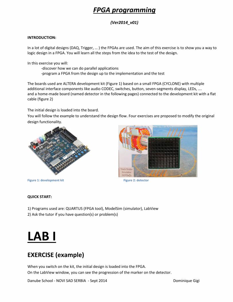
The boards used are ALTERA development kit (Figure 1) based on a small FPGA (CYCLONE) with multiple additional interface components like audio CODEC, switches, button, seven-segments display, LEDs, …. and a home-made board (named detector in the following pages) connected to the development kit with a flat cable (figure 2)
The initial design is loaded into the board.
You will follow the example to understand the design flow. Four exercises are proposed to modify the original
design functionality.
Figure 1: development kit Figure 2: detector
QUICK START:
1) Programs used are: QUARTUS (FPGA tool), ModelSim (simulator), LabView
2) Ask the tutor if you have question(s) or problem(s)
LAB I EXERCISE (example)
When you switch on the kit, the initial design is loaded into the FPGA.
On the LabView window, you can see the progression of the marker on the detector.

Danube School - NOVI SAD SERBIA - Sept 2014 Dominique Gigi
At the same time, you can see on the two 7-segments LED (the right ones on ALTERA kit) the column and the line
number over which the maker is positioned.
DESIGN ENTRY
The design file is named “CII_Starter_Default.bdf” (for all exercises you should work with the same design file).
The design is divided in three parts:
a) A green rectangle which is used to transmit the information to the computer via the RS232 connection to
display the trace on LabView.
b) A blue rectangle in which the design generates the clock and the logic to control the detector (see
Appendix A for detailed functionality).
c) A red rectangle, which contains the logic to detect the trace. You will change the logic in this rectangle in
the following exercises.
The idea of all exercises is to detect a trace. As soon as the trace is detected one 7-segment LED blinks (the third
for the right side).
Click on key0 (Altera kit) to stop the blinking. Now generate another trace.
Spend some time to understand how this design works.
Do you understand it?
COMPILATION
This design is the entry of your logic, it should be compiled now; go to QUARTUS Processing->Start Compilation.
The design is compiled for the chosen component (Cyclone II).
The compiler executes multiple tasks:
logic optimization
generates a binary file used to program the FPGA (memory array),
extracts the timing between each logic elements used for the timing analyses
generate an output VHDL file used for the simulation
SIMULATION
When the compilation is finished, you can check the design with a simulator. To do this you will use ModelSim.
Check in the “Project” TAB if there is a file marked with a bleu “?”, if YES, compile it (right-clic on it, Compile->
compile selected)
In the “Transcript” tab, type ‘source sim.tcl’, ENTER. The simulator opens the waveform, loads the signals, and
starts the simulation.
At the end, stimuli and results are displayed in the wave window.
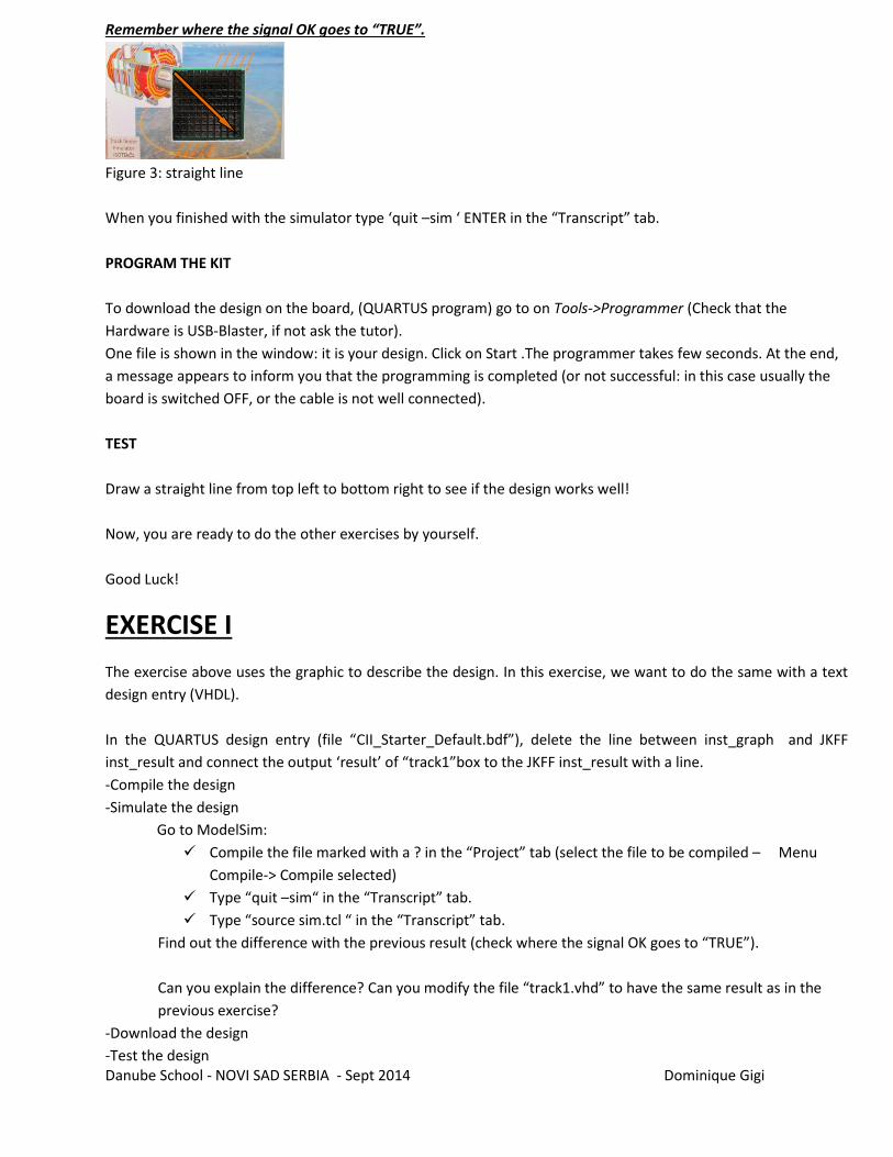
This simulation emulates a trace starting from the top left and finishing at bottom right describing a straight line
on the detector.
(The tutor will give you some explanations on the results and the signals shown in the waveform)
Danube School - NOVI SAD SERBIA - Sept 2014 Dominique Gigi
Remember where the signal OK goes to “TRUE”.
Figure 3: straight line
When you finished with the simulator type ‘quit –sim ‘ ENTER in the “Transcript” tab.
PROGRAM THE KIT
To download the design on the board, (QUARTUS program) go to on Tools->Programmer (Check that the
Hardware is USB-Blaster, if not ask the tutor).
One file is shown in the window: it is your design. Click on Start .The programmer takes few seconds. At the end,
a message appears to inform you that the programming is completed (or not successful: in this case usually the
board is switched OFF, or the cable is not well connected).
TEST
Draw a straight line from top left to bottom right to see if the design works well!
Now, you are ready to do the other exercises by yourself.
Good Luck!
EXERCISE I
The exercise above uses the graphic to describe the design. In this exercise, we want to do the same with a text
design entry (VHDL).
In the QUARTUS design entry (file “CII_Starter_Default.bdf”), delete the line between inst_graph and JKFF
inst_result and connect the output ‘result’ of “track1”box to the JKFF inst_result with a line.
-Compile the design
-Simulate the design
Go to ModelSim:
Compile the file marked with a ? in the “Project” tab (select the file to be compiled – Menu
Compile-> Compile selected)
Type “quit –sim“ in the “Transcript” tab.
Type “source sim.tcl “ in the “Transcript” tab.
Find out the difference with the previous result (check where the signal OK goes to “TRUE”).
Can you explain the difference? Can you modify the file “track1.vhd” to have the same result as in the
previous exercise?
-Download the design
-Test the design
Danube School - NOVI SAD SERBIA - Sept 2014 Dominique Gigi
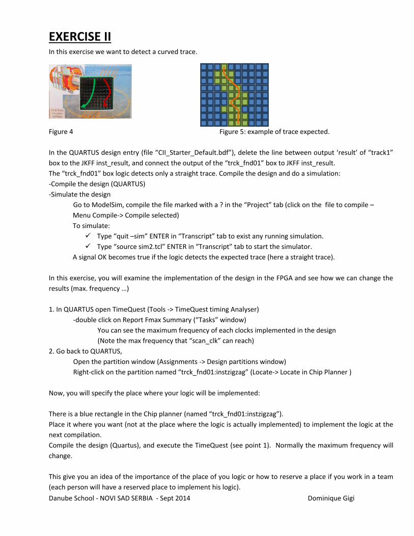
EXERCISE II In this exercise we want to detect a curved trace.
Figure 4 Figure 5: example of trace expected.
In the QUARTUS design entry (file “CII_Starter_Default.bdf”), delete the line between output ‘result’ of “track1”
box to the JKFF inst_result, and connect the output of the “trck_fnd01” box to JKFF inst_result.
The “trck_fnd01” box logic detects only a straight trace. Compile the design and do a simulation:
-Compile the design (QUARTUS)
-Simulate the design
Go to ModelSim, compile the file marked with a ? in the “Project” tab (click on the file to compile –
Menu Compile-> Compile selected)
To simulate:
Type “quit –sim” ENTER in “Transcript” tab to exist any running simulation.
Type “source sim2.tcl” ENTER in “Transcript” tab to start the simulator.
A signal OK becomes true if the logic detects the expected trace (here a straight trace).
In this exercise, you will examine the implementation of the design in the FPGA and see how we can change the
results (max. frequency …)
1. In QUARTUS open TimeQuest (Tools -> TimeQuest timing Analyser)
-double click on Report Fmax Summary (“Tasks” window)
You can see the maximum frequency of each clocks implemented in the design
(Note the max frequency that “scan_clk” can reach)
2. Go back to QUARTUS,
Open the partition window (Assignments -> Design partitions window)
Right-click on the partition named “trck_fnd01:instzigzag” (Locate-> Locate in Chip Planner )
Now, you will specify the place where your logic will be implemented:
There is a blue rectangle in the Chip planner (named “trck_fnd01:instzigzag”).
Place it where you want (not at the place where the logic is actually implemented) to implement the logic at the
next compilation.
Compile the design (Quartus), and execute the TimeQuest (see point 1). Normally the maximum frequency will
change.
This give you an idea of the importance of the place of you logic or how to reserve a place if you work in a team
(each person will have a reserved place to implement his logic).
Danube School - NOVI SAD SERBIA - Sept 2014 Dominique Gigi
NB: For your information, for each clock of the design, the frequency to reach has to be specified in a constraint
file.
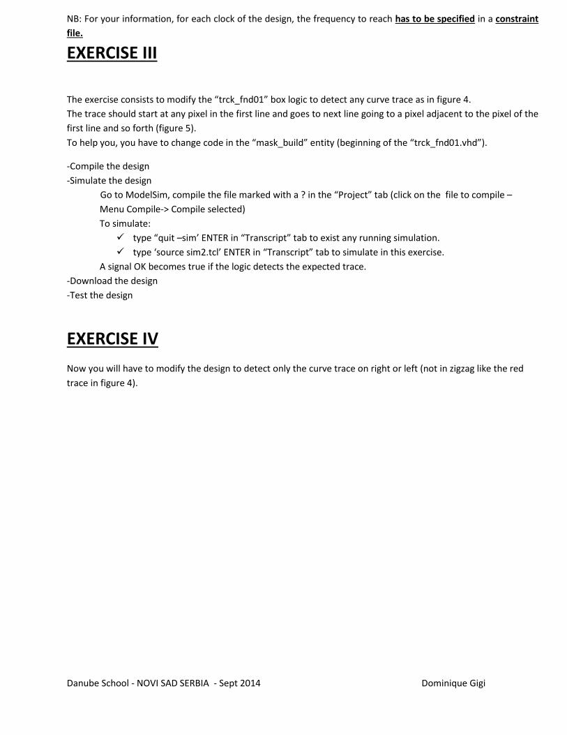
EXERCISE III
The exercise consists to modify the “trck_fnd01” box logic to detect any curve trace as in figure 4.
The trace should start at any pixel in the first line and goes to next line going to a pixel adjacent to the pixel of the
first line and so forth (figure 5).
To help you, you have to change code in the “mask_build” entity (beginning of the “trck_fnd01.vhd”).
-Compile the design
-Simulate the design
Go to ModelSim, compile the file marked with a ? in the “Project” tab (click on the file to compile –
Menu Compile-> Compile selected)
To simulate:
type “quit –sim’ ENTER in “Transcript” tab to exist any running simulation.
type ‘source sim2.tcl’ ENTER in “Transcript” tab to simulate in this exercise.
A signal OK becomes true if the logic detects the expected trace.
-Download the design
-Test the design
EXERCISE IV
Now you will have to modify the design to detect only the curve trace on right or left (not in zigzag like the red
trace in figure 4).
Danube School - NOVI SAD SERBIA - Sept 2014 Dominique Gigi
APPENDIX A
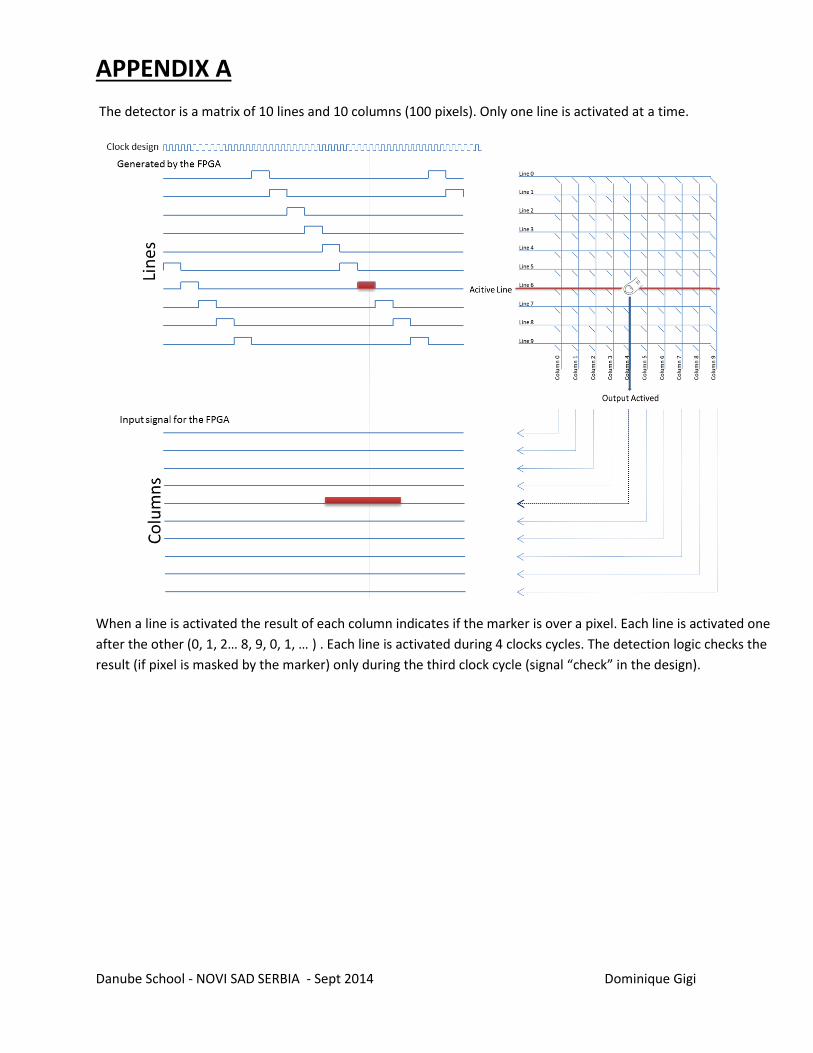
The detector is a matrix of 10 lines and 10 columns (100 pixels). Only one line is activated at a time.
When a line is activated the result of each column indicates if the marker is over a pixel. Each line is activated one
after the other (0, 1, 2… 8, 9, 0, 1, … ) . Each line is activated during 4 clocks cycles. The detection logic checks the
result (if pixel is masked by the marker) only during the third clock cycle (signal “check” in the design).

Danube School - NOVI SAD SERBIA - Sept 2014 Dominique Gigi
LAB II In this second lab, you will discover a third possibility to implement design in a FPGA, using the IP (Intellect
Property) core. Which is a element (counter, memory interface, PCI interface) that you can parameterize to meet
your requirements.
You will approach also the importance on the setup and hold time, that IO (input/output) should meet.
And to finish you will see that the simulation can be customize and that it is the most important task in the FPGA
development.
EXERCISE (example) This design uses
-3 buttons (KEY0: reset; KEY1: start; KEY2: stop)
-4 seven-segments displays
This design is on the kit by default (at power ON).
When you click on KEY1, the counter starts and displays its value (in hexadecimal) on the seven-segment.
When you click on KEY2, the counter stop to count.
When you click on KEY0 the counter is reset to 0000.
DESIGN ENTRY
The design file is named “CII_Starter_Default.bdf” (for all exercises you should work with the same design file).
The design can be divided in four parts: from the left INPUT, counter, converter (hexa to 7seg), OUTPUT. If
you click on the element named counter, a window (figure 2) is opened.
Figure 2: Mega Wizard window (1) Figure 3: Mega Wizard display (2)
Danube School - NOVI SAD SERBIA - Sept 2014 Dominique Gigi
You can see the characteristics of the counter (4 bits, count up).
If you click on “Next >”, you can see the other characteristics of this counter. And
the end (Figure 3), click on “Finish”
If you click on the “CONV_H_7SEG”, a text (VHDL or AHDL language) file will be opened. It contains the
functionality of this entity. (Don’t spend time to understand this logic, it converts value to be displayed on seven
segment elements).
You can see also the buttons represented by INPUTS, and seven-segment elements represented by OUTPUTS.
Spend 10 minutes to understand how this design works.
Do you understand?
COMPILATION
This design is the entry of your logic, it should be compiled now; go to Processing->Start Compilation.
The design is compiled for the chosen component (Cyclone II).
The compiler generates: logic optimization, the binary file to program the FPGA (memory array), the timing
between each logic elements (used for the simulation).
SIMULATION
Open Modelsim, (ask the instructor to setup the project).
Take attention that all files are compiled (no question mark!)
In the transcript window, type “sim.tcl”.
The simulation will start.
Check the result of the simulation. Is there something that is difficult to understand or to check ?
PROGRAM THE KIT
To download the design on the board, go to on Tools->Programmer (Check that the Hardware is USB-Blaster, if
not ask the instructor).
One file is existed in the window, it is your design. Click on Start .The programmer takes some seconds. At the
end, a message appears to inform you that the programming download is completed (or not successful: usually
the board is switch on OFF, or the cable is not well connected).
Danube School - NOVI SAD SERBIA - Sept 2014 Dominique Gigi
TEST
Now, you are ready to do the other exercises yourself.
Good Luck!
EXERCISE I Use the example described above, and change the logic to count only while button KEY1 is pushed down. To help
you in all the exercises, you can find a summary of the elements you should use with their truth table in the last
page (Appendix B)
To enter an element, double click anywhere on the design entry file (not on a symbol already in the entry file).
-Modify the design
-Compile the design
-Simulate the design (use still “sim1.tcl” to simulate your design)
-Download the design
-Test the design
EXERCISE II
In this exercise, you have to modify the design to have a counter that can count up or down. The choice of count
up/down is done with SW[9] INPUT (already in the design).
HELP (you do not have to add any element)
-Modify the design
-Compile the design
-Simulate the design
Here, you will have to change the stimuli (file: “CII_Starter_Default1.vhd”) to check if your implementation is well
done. (Ask the instructor to know where the file is).
Use “sim1.tcl” to simulate your design.
-Download the design
-Test the design

Danube School - NOVI SAD SERBIA - Sept 2014 Dominique Gigi
EXERCISE III
In this exercise, the count should count in decimal and not in hexadecimal.
-Modify the design
-Compile the design
-Simulate the design
Use “sim1.tcl” to simulate your design.
-Download the design
-Test the design
Danube School - NOVI SAD SERBIA - Sept 2014 Dominique Gigi
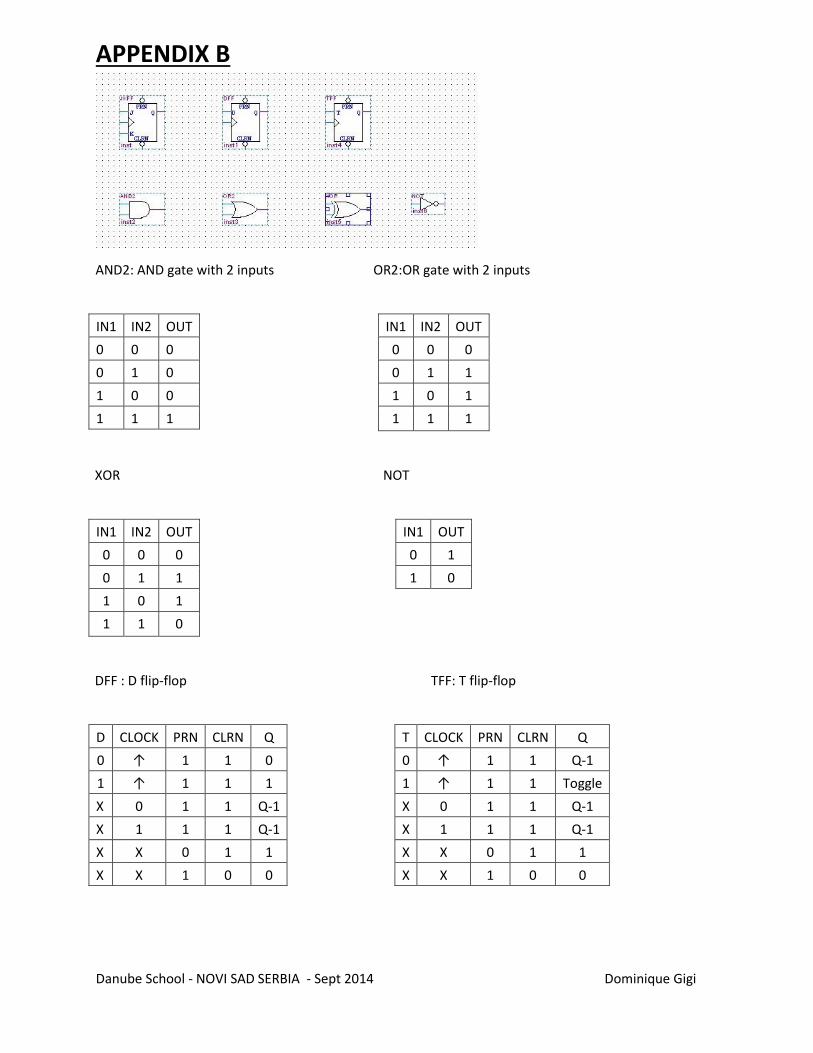
APPENDIX B
AND2: AND gate with 2 inputs OR2:OR gate with 2 inputs
IN1 IN2 OUT
0 0 0
0 1 0
1 0 0
1 1 1
IN1 IN2 OUT
0 0 0
0 1 1
1 0 1
1 1 1
XOR NOT
IN1 IN2 OUT
0 0 0
0 1 1
1 0 1
1 1 0
IN1 OUT
0 1
1 0
DFF : D flip-flop TFF: T flip-flop
D CLOCK PRN CLRN Q
0 ↑ 1 1 0
1 ↑ 1 1 1
X 0 1 1 Q-1
X 1 1 1 Q-1
X X 0 1 1
X X 1 0 0
T CLOCK PRN CLRN Q
0 ↑ 1 1 Q-1
1 ↑ 1 1 Toggle
X 0 1 1 Q-1
X 1 1 1 Q-1
X X 0 1 1
X X 1 0 0
Danube School - NOVI SAD SERBIA - Sept 2014 Dominique Gigi
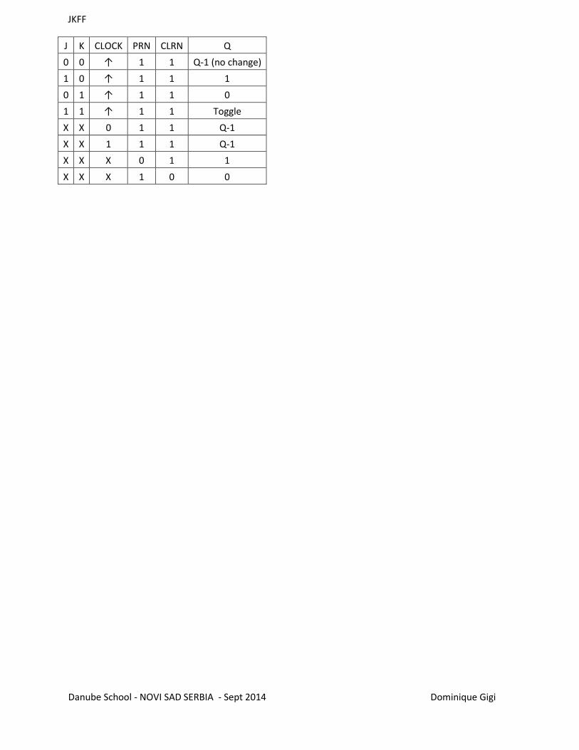
JKFF
J K CLOCK PRN CLRN Q
0 0 ↑ 1 1 Q-1 (no change)
1 0 ↑ 1 1 1
0 1 ↑ 1 1 0
1 1 ↑ 1 1 Toggle
X X 0 1 1 Q-1
X X 1 1 1 Q-1
X X X 0 1 1
X X X 1 0 0