Embed Size (px)
Citation preview
LAB EXERCISE 4.1 ·Minterm and In this lab exercise you will learn the use of minterm and
Maxterm Truth maxterm truth tables. You will also demonstrate theTables equivalence of the minterm and maxterm fonns of a logic
Objectives expression.
Materials LD-2 Logic Designer
74LS08 Quad 2-Input AND
74LS11 Triple 3-Input AND
74LS32 Quad 2-Input OR
Jumper Wires (See Figt?Ie 4-28 for Ie pinouts.) ~P
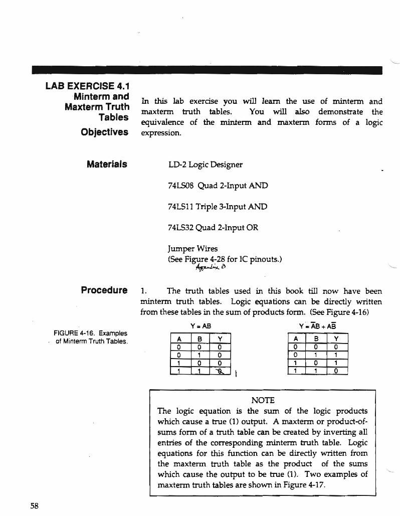
Procedure 1. The truth tables used in this book till now have been minterm truth tables. Logic equations can be directly written from these tables in the sum of products form. (See Figure 4-16)
FIGURE 4-16. Examples of Minterm Truth Tables. A B Y
0 0 0 0 1 0 1 0 0, 1 ""9..
A B Y 0 0 0 0 1 1, 0 1 1 1 0
NOTE The logic equation is the sum of the logic products which cause a true (1) output. A maxterm or product-ofsums form of a truth table can be created by inverting all entries of the corresponding minterm truth table. Logic equations for this function can be directly written from the maxterm truth table as the product of the sums which cause the output to be true (1). Two examples of maxterm truth tables are shown in Figure 4-17.
58
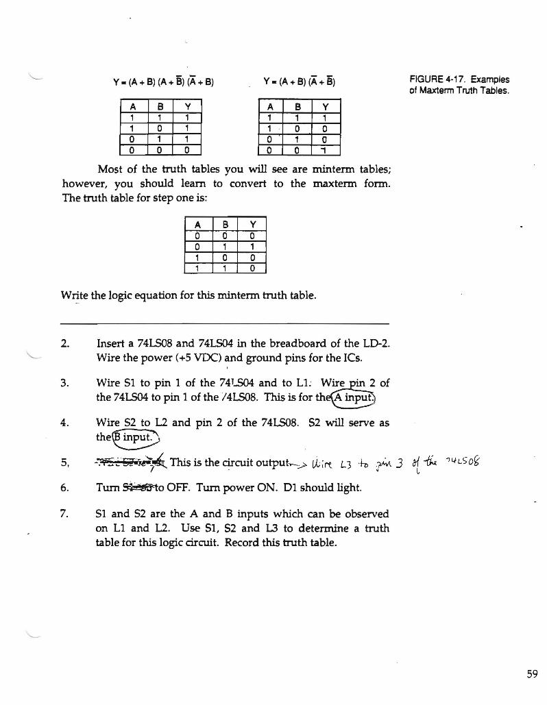
Y ., (A + B) (A + B) (A +B) Y • (A + B) (A + B) FIGURE 4·17. Examples of Maxterm Truth Tables.
A B Y 1 1 1 1 0 1 0 1 1 0 0 0
A B Y 1 1 1 1 0 0 0 1 0 0 0 "1
Most of the truth tables you will see are minterm tables; however, you should learn to convert to the maxterm form. The truth table for step one is:
A B Y 0 0 0 0 1 ,, 0 0, , 0
Write the logic equation for this minterm truth table.
2. Insert a 74LSOB and 74L504 in the breadboard of the LD-2. Wire the power (+5 VDC) and ground pins for the ICs.
,
3. Wire 51 to pin 1 of the 741..504 and to LL ~=§ of the 74LS04 to pin 1 of the 14LSOB. This is for th A input.
4. Wire 52 to L2 and pin 2 of the 74LSOB. 52 will serve as
the~
5, -:f5.:"-Qi.~4z. This is the ~cuit output~.:> th~rt L3 .~ :M 3 ~ 1k. "(hSo~
6. Turn ~o OFF. Turn power ON. D1 should light.
7. 51 and 52 are the A and B inputs which can be observed on L1 and L2. Use 51, 52 and L3 to determine a truth table for this logic circuit. Record this truth table.
59
8. Form the maxterm truth table for the truth table in step 7. Write equations ' for this function in product of sums form.
9. Remove the circuit used in step 7. Insert a 74LS04, 74LS32 and 74LSll into the LD-2 breadboard. Wire power and ground to these circuits.
10. Wire 51 to pin 1 of the 74LS04, pin 1 of the 74LS32 an@ ~
Thisis~
11. Wire pin 2 of the 74LS04 to pins 5 and 9 of the 74LS32.
12. Wire 52 to pin .3 o~theLS04, Bkd pins 2 and 4 of the 74LS32. This is the inptrt)---.
13. Wire pin 4 of the 74LS04 to pin 10 of the 74LS32.
14. Wire pins 3, 6 and 8 of the 74LS32 to pins 3,4 and 5 respectively on the 74LSll.
15: Wir~e 74LS11~ This allows mOnitoring the~ "-./
16. Tum all logic switches to OFF. Tum ON power. D1 should light.
17. 51 is A, 52 is B, and L3 is the logic circuit output. Use 51, 52, and L3 to construct a truth table for this circuit. Record the truth table here. Leave the circuit connected and answer the follOwing questions.
60
1. Compare the truth tables from steps 7 and 17. What do Questions you notice about them?
2. Draw schematic diagrams of the circuits that produced the truth tables in steps 7 and 17.
3. Which circuit better performs this logic function? (step 7 or step 17 ?). Why?
LAB EXERCISE 4.2 Simplifying Logic CircuitsIn this lab exercise you will study and apply techniques to reduce
redundant logic elements in combinational logic circuits. Objectives 61
Materials LD-2 logic Designer
74LS04 Hex Inverter
74LSOB Quad 2-Input AND
74LS27 Triple 3-Input NOR
74LS32 Quad 2-Input OR
Jumper Wires (Ref. Figure 4-2B for IC pinouts.)
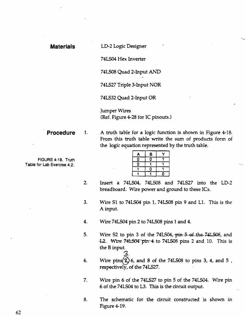
Procedure I. A truth table for a logic function is shown in Figure 4-1B. From this truth table write the sum of products fonn of the logic equation represented by the truth table.
FIGURE 4-18. Truth Table for Lab Exercise 4.2.
A B Y 0 0 1 0 1 1 1 0 1 1 1 0
2. Insert a 74LS04, 74LSOB and 74LS27 into the LD-2 breadboard. Wire power and ground to these ICs.
3. Wire 51 to 74LS04 pin 1, 74LSOB pin 9 and Ll. This is the A input.
4. Wire 74LS04 pin 2 to 74LSOB pins I and 4.
5. Wire 52 to pin 3 of the 74LS04, ~74LSG8, and -1.2. Wire 74L904 p1n-4- to 74LSOB pins 2 and 10. This is the B input.
21 6. Wire pms@ 6, and B of the 74LSOB to pins 3, 4, and 5 ,
respectively, of the 74LS27.
7. Wire pin 6 of the 74LS27 to pin 5 of the 74LS04. Wire pin 6 of the 74LS04 to L3. This is the circuit output.
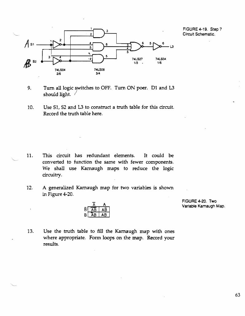
B. The schematic for the circuit constructed is shown in Figure 4-19.
62
'
A51
I> 52
2
• 5
~ 3 III 7.LS27 7.L504
113. 116
7.L5~ 7.LS08 2/6 3/.
9. Tum all logic switches to OFF. Turn ON poer. Dl and L3 should light. /
10. Use 51, 52 and L3 to construct a truth table for this circuit. Record the truth table here.
11. This circuit has redundant elements. It could be converted to function the same with fewer components. We shall use Kamaugh maps to reduce the logic circuitry.
12. A generalized Kamaugh map for two variables is shown in Figure 4-20.
13. Use the truth table to fill the Kamaugh map with ones where appropriate. Form loops on the map. Record your results.
FIGURE 4-19. Step 7 Circuit Schematic.
FIGURE 4-20. Two Variable Kamaugh Map.
63
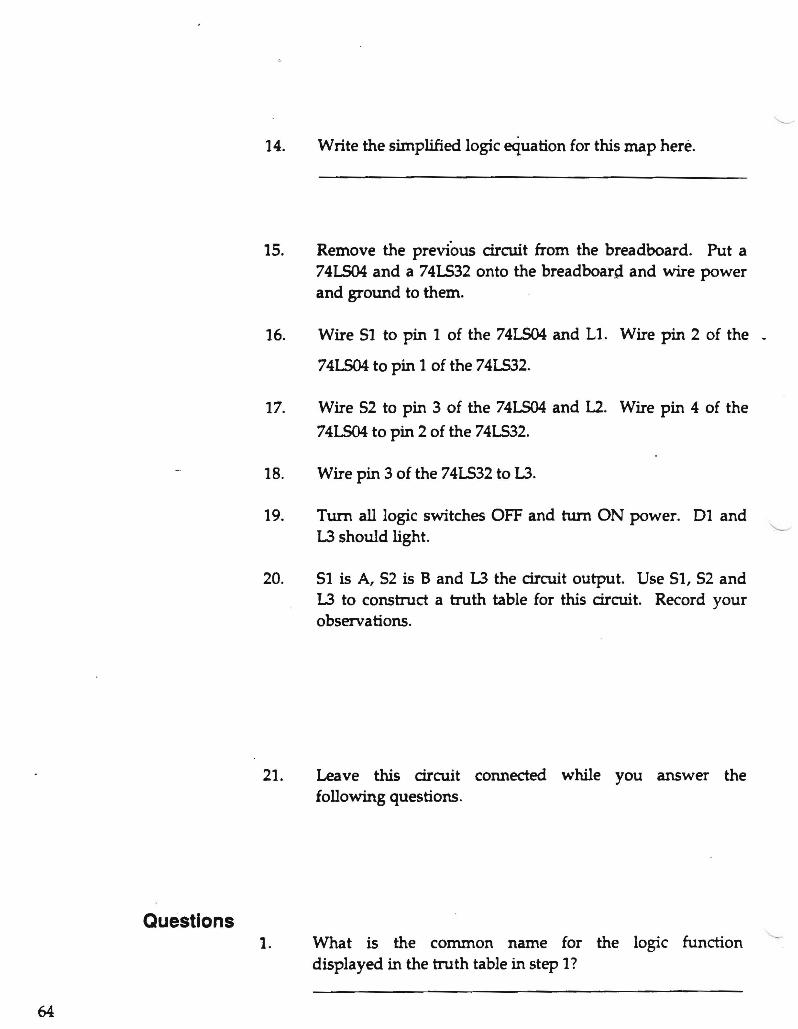
14. Write the simplified logic equation for this map here.
15. Remove the previous circuit from the breadboard. Put a 74L504 and a 74LS32 onto the breadboard and wire power and ground to them.
16. Wire 51 to pin 1 of the 74LS04 and Ll. Wire pin 2 of the _
74L504 to pin 1 of the 74LS32.
17. Wire 52 to pin 3 of the 74LS04 and L2. Wire pin 4 of the
74LS04 to pin 2 of the 74LS32.
18. Wire pin 3 of the 74LS32 to L3.
19. Tum all logic switches OFF and tum ON power. D1 and 1.3 should light.
20. 51 is A, 52 is Band L3 the circuit output. Use 51, 52 and L3 to construct a truth table for this circuit. Record your observations.
21. Leave this circuit connected while you answer the following questions.
Questions 1. What is the common name for the logic function
displayed in the truth table in step 1?
64
2. What do you notice about the truth tables resulting ,from steps 10 and 20 ?
3. What do you call the simplified logic equation from the results of step 14 ?
4. Which of the circuits is better to use? Why?
You will learn about decoders in this lab exercise. - sl1fdy the simple decoder and the one of four decoder.
You will LAB EXERCISE 4.3 Decoders Objectives
LD-2 Logic Designer Materials
74L504 Hex Inverter.
74LS08 Quad 2-Input AND
74L511 Triple 3-Input AND
Jumper Wires (Ref. Figure 4-28 for Ie pinouts.)
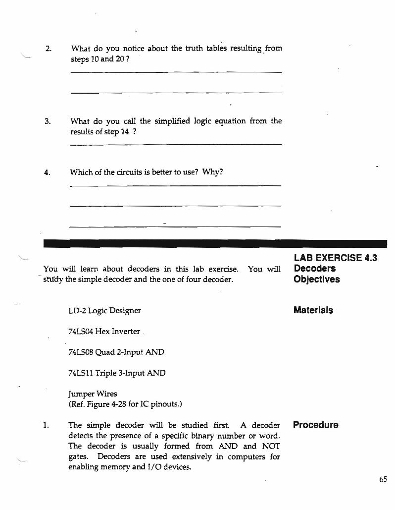
1. The simple decoder will be studied first. A decoder detects the presence of a specific binary number or word. The decoder is usually formed from AND and NOT gates. Decoders are used extensively in computers for enabling memory and I/O devices.
Procedure
65
.'
2.
FIGURE 4·21. Schematic of a Simple Decoder.
3.
4.
5.
6.
7.
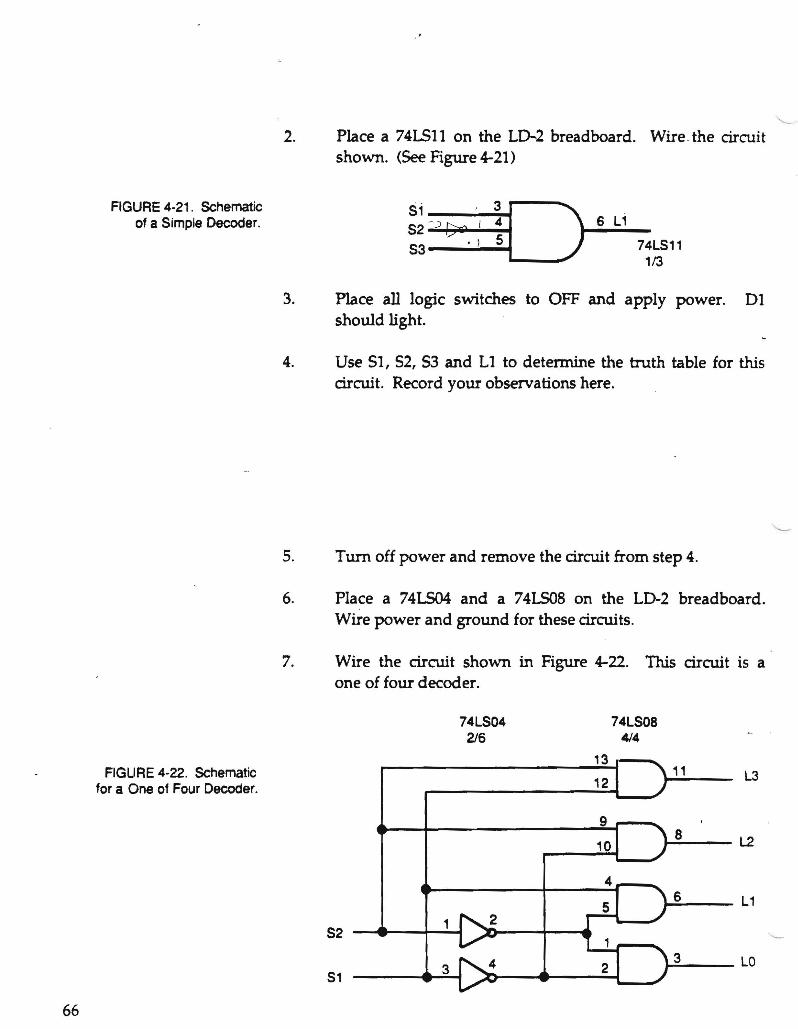
FIGURE 4-22. Schematic for a One of Four Decoder.
Place a 74LS11 on the LD-2 breadboard. Wire. the circuit shown. (See Figure 4-21)
51 ' 31 )~~ -~ [;ro. )t ~ ..___ .._6_L_1_7-~;511
Place all logic switches to OFF and apply power. D1 should light.
Use 51, 52, 53 and L1 to determine the truth table for this circuit. Record your observations here.
Turn off power and remove the circuit from step 4.
Place a 74LS04 and a 74LS08 on the LD-2 breadboard. Wire power and ground for these circuits.
Wire the circuit shown in Figure 4-22. This circuit is a one of four decoder.
74L504 74LS08 216 414
13 11 L3
9 8 L2
6 L1
S2 -1
---t--1
3
12
10
2
.....
~3___ LO
51
66

·B. Tum the logic switches to OFF. Tum ON power. 01 and LO should light.
9. Use 51, 52 and LO-L3 to form a table of the circuit operation.
10. Leave the circuit wired while you answer the following questions.
Questions 1. What binary number does the circuit form step 4 decode?
2. Name one use of a circuit like the one in Figure 4-6.
3. Explain the operation of the one of four decoder.
4. Design a circuit to decode 101 binary.
5. Circuits similar to the one of four decoder are used to convert from BCO to decimal. How many AND gates will be required to implement such a circuit? Hint: Examine Figure 4-22 schematic.
67
·'
6. 'Why can't the logic equation from the truth table of step 9 be written as y =AB + AB + AB + AB ?
LAB EXERCISE 4.4 In this lab exercise encoders will be studied. Encoders accept one Encoders or more inputs and generate a mutli-bit binary output. You will
. study a simple encoder. The basic encoder circuit is the positive Objectives NAND gate.
Materials LD-2 Logic Designer
74LSOO Quad 2-Input NAND
Jumper Wires (Ref. Figure 4-28 for Ie pinouts.)
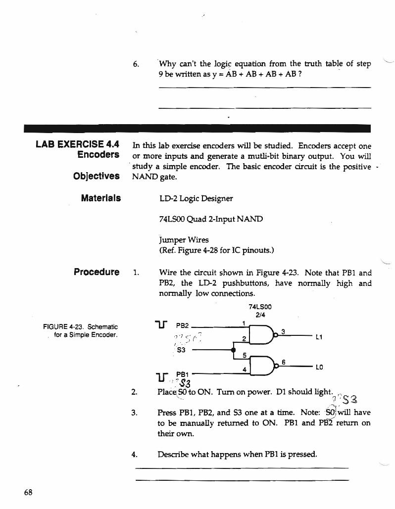
Procedure 1. Wire the circuit shown in Figure 4-23. Note that PBI and PB2, the LD-2 pushbuttons, have nonnally high and normally low connections.
74LSOO 2/4
FIGURE 4-23. Schematic 1f PB2-----------~r-~ 3 , for a Simple Encoder. ,, ' 1 coO (,--; g...;;;------- L12.....J •
I . . "
.'53
6 p-;;.---- LO4
1f PB1 .i ..~..s3
2. Place;SO to ON. Tum on power. Dl should light. ,_,' -. .~ 'S:3
.--""'t> •
3. Press PB1, PB2, and 53 one at a time. Note:~will have to be manually returned to ON. PBl and PB2 return on their own.
4. Describe what happens when PBl is pressed.
68
5. Record your observation when PB2 is pressed.
6. Place SO to OFF. Record your observations.
7. Return SO to ON.
8. Remove power from the circuit.
1. What does the circuit of step one do ? Questions
LAB EXERCISE 4.5 Exclusive OR Circuits
In this lab exercise the exclusive OR (EXOR) circuit and some applications of EXOR circuits will be studied. Objectives
LD-2 logiC Designer Materials
74LS04 Hex Inverter
74LS08 Quad 2-Input NAND
74L532 Quad 2-Input OR
74L586Quad EXOR
Jumpers (Ref. Figure 4-28 for Ie pinouts.)
69
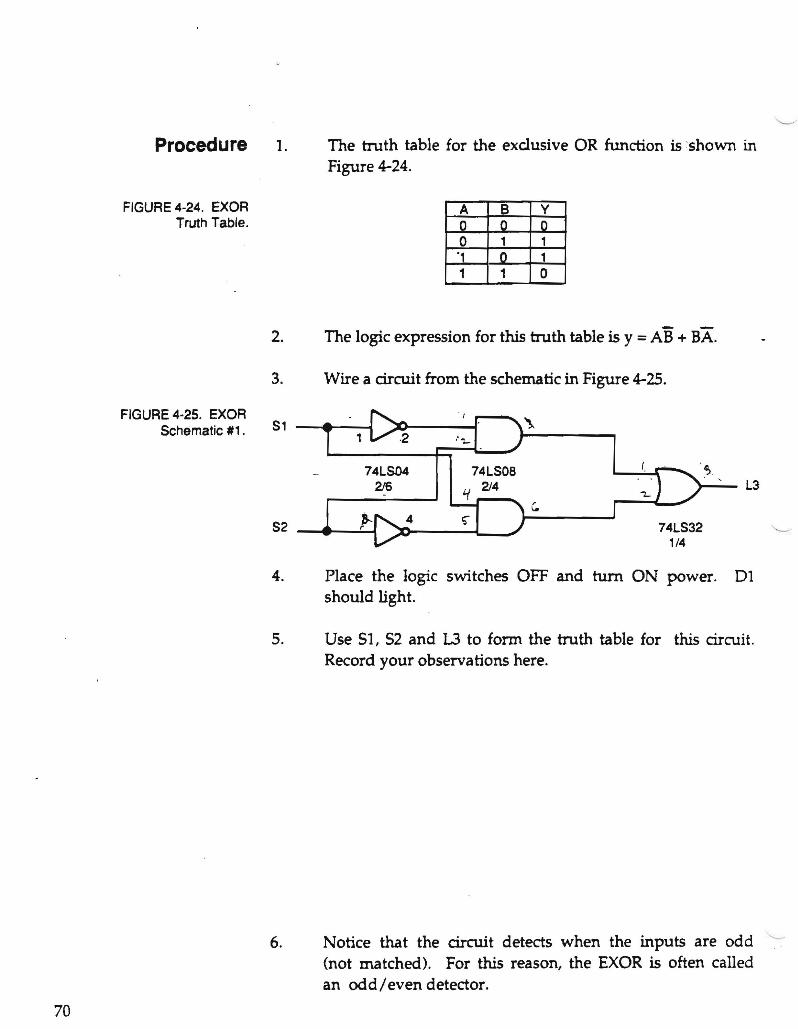
Procedure 1. The truth table for the exclusive OR function is :shown in Figure 4-24.
FIGURE 4-24. EXOR Truth Table.
A B Y Q 0 0 0 1 1., 0 1 1 1 0
2. The logic expression for this truth table is y = AB + BA.
3. Wire a circuit from the schematic in Figure 4-25.
FIGURE 4·25. EXOR Schematic '1. S1 - __----t
·2
74LS04 74LSOB 2/4216 >-- L3
S2 74LS32 1/4
4. Place the logic switches OFF and turn ON power. D1 should light.
5. Use S1, 52 and 13 to form the truth table for this circuit. Record your observations here.
6. Notice that the circuit detects when the inputs are odd "(not matched). For this reason, the EXOR is often called an odd/even detector.
70
.'
'-- 7. Turn OFF power to the circuit. Remove the ICs from the breadboard.
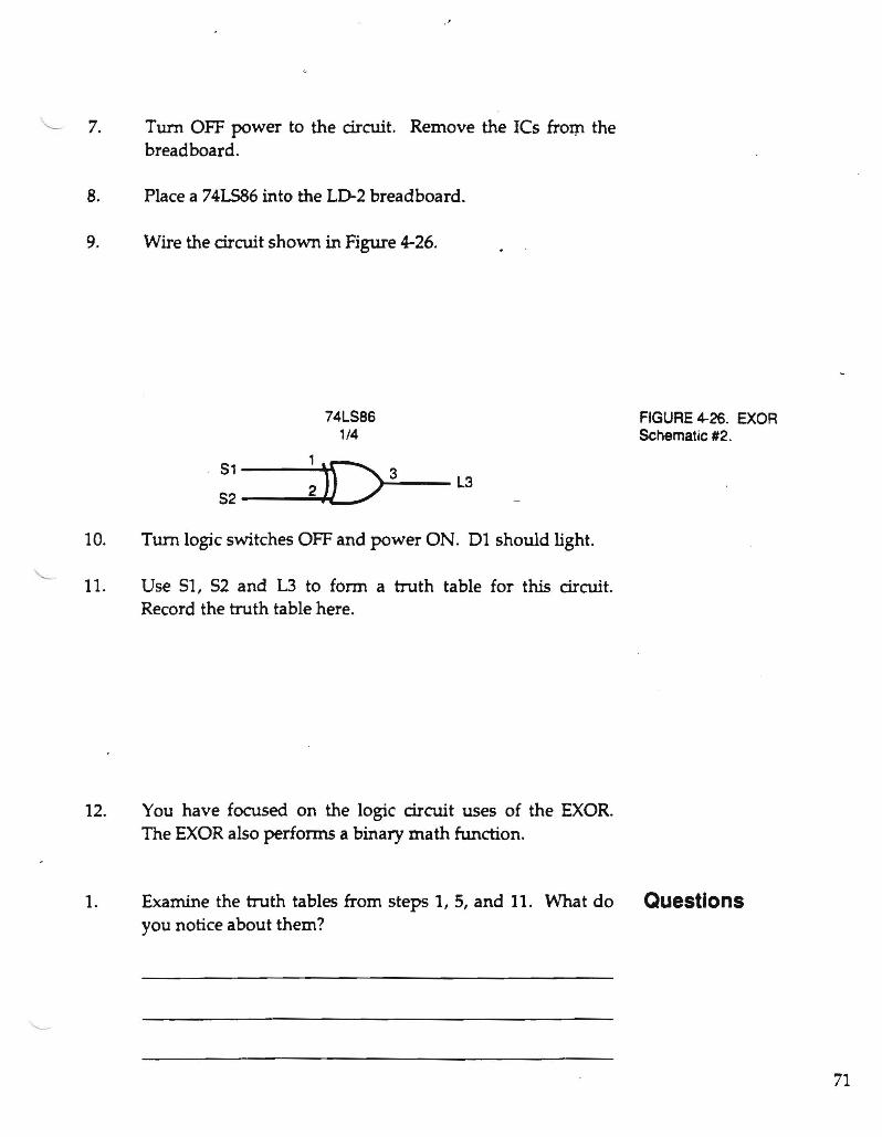
8. Place a 74LS86 into the LD-2 breadboard.
9. Wire the circuit shown in Figure 4-26.
74LS86 1/4
:~ ____:+D....3~_- L3
10. Turn logic switches OFF and power ON. Dl should light.
11. Use 51, 52 and L3 to form a truth table for this circuit. Record the truth table here.
12. You have focused on the logic circuit uses of the EXOR. The EXOR also perfonns a binary math function.
1. Examine the truth tables from steps 1, 5, and 11. What do you notice about them?
FIGURE 4-26. EXOR Schematic #2.
Questions
71
·2. What math function does the EXOR gate perfonn ?
3. Which circuit is better to use, the one from step 3 or the one from step 9? Why?
4. Draw the Kamaugh map for the EXOR. Can this be reduced?
LAB EXERCISE 4.6 The EXNOR Circuit
Objectives In this lab exercise the EXNOR circuit will be studied.
Materials LD-2 Logic Designer
74LS04 Hex Inverter
74LSB6 Quad EXOR
72
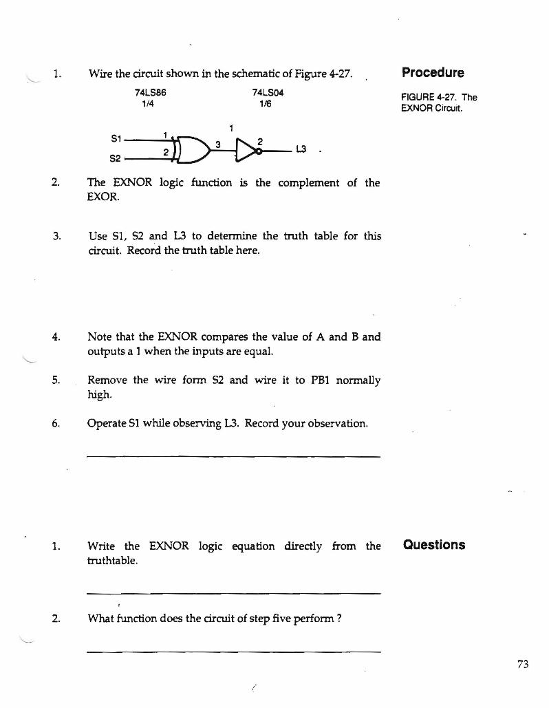
1. Wire the drcuit shown in the schematic of Figure 4-27. Procedure 74LS86 74LS04 FIGURE 4-27. The 1~ 1~ EXNOR Circuit.
S1 L3 .:D3
, ~S2
2. The EXNOR logic function is the complement of the EXOR.
3. Use 51, 52 and L3 to detennine the truth table for this circuit. Record the truth table here.
4. Note that the EXNOR compares the value of A and Band outputs a 1 when the inputs are equal.
5. Remove the wire form 52 and wire it to PBl normally high.
6. Operate 51 while observing L3. Record your observation.
1. Write the EXNOR logic equation directly from the Questions truthtable.
2. What function does the drcuit of step five perform ?
(
73

3. Make a Kainaughmap for the EXNOR function. _Can this function be reduced ?
74