Embed Size (px)
Citation preview
EE221-2016 Laboratory #3 2016-09-29
Rev A Copyright 2016 © University of Saskatchewan Page 1 of 12
Lab 3: BJT I-V Characteristics
1. Learning Outcomes At the end of this lab, students should know how to theoretically determine the I-V (Current-Voltage) characteristics of both NPN and PNP Bipolar Junction Transistors (BJT), know how to experimentally determine the I-V characteristics, and have a good understanding of what they mean.
2. Health and Safety Any laboratory environment may contain conditions that are potentially hazardous to a person’s health if not handled appropriately. The Electrical Engineering laboratories obviously have electrical potentials that may be lethal and must be treated with respect. In addition, there are also mechanical hazards, particularly when dealing with rotating machines, and chemical hazards because of the materials used in various components. Our LEARNING OUTCOME is to educate all laboratory users to be able to handle laboratory materials and situations safely and thereby ensure a safe and healthy experience for all. Watch for posted information in and around the laboratories, and on the class web site.
3. Lab Report Students work in groups of 2 with laboratories being on alternative week (in 2C80/82). Each student must have a lab book for the labs. The lab book is used for lab preparation, notes, record, and lab reports. The lab books must be handed before 5:00 pm on the due date (same day of the following week) into the box labeled for your section across from 2C94.
4. Background The BJT is best described as a current-controlled active element (while the MOSFET and JFET are voltage-controlled). The base current iB is usually considered the controlling quantity, controlling the collector current iC. Although iB in turn depends upon vBE (base-emitter voltage), the change in vBE for a given change in iB is so small because of the exponential relationship that is often neglected. This approximation (vBE =0.7 V) is often a source of confusion for the students who do not realize that a truly constant vBE implies no change in iB.
5. Material and Equipment
Material (supplied by department)
Equipment (supplied by student)
2N2222A (NPN Transistor) Analog Discovery
2N2907A (PNP Transistor) Waveforms 2015 software
Resistors: 1 x 100 Ω, 1 x 22 kΩ Breadboard and wiring kit

EE221-2016 Laboratory #3 2016-09-29
Rev A Copyright 2016 © University of Saskatchewan Page 2 of 12
6. Prelab 1. For each of:
1.1. 2N2222A (NPN Transistor)
1.2. 2N2907A (PNP Transistor)
Look up the characteristics of each device by doing a web search. Fill in the following table for each of the devices:
Rating/Characteristic Value Maximum Collector-Emitter Voltage Maximum Continuous Collector Current DC Current Gain (hFE) Collector-Emitter Saturation Voltage Base-Emitter Saturation Voltage Small-Signal Current Gain (hfe)
2. A SPICE circuit file for the 2N2222A circuit (Figure 7-1) is given in Figure 6-1. Using LTspice (a guide to using LTspice can be found in Laboratory #1 – Appendix A), include a screen capture of the plot of the I-V characteristics of the 2N2222A in your lab report.
2.1. The horizontal axis should be set to "V(vc)". To set the horizontal axis, mouse over any of the numbers listed in the horizontal axis and "click" to bring up the "Horizontal Axis" dialog.
2.2. The vertical axis should be set to "Ic(Q1)" (using "Plot Settings | Add Trace").
2.3. The plot should look similar to Figure 6-2.
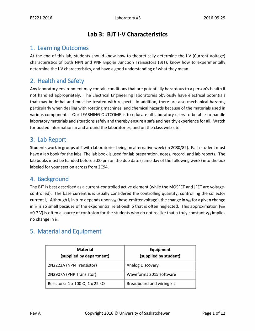
3. The SPICE model for a 2N2907A Transistor is given in Figure 6-3. Modify the SPICE circuit file shown in Figure 6-1 to simulate the 2N2907A circuit shown in Figure 7-7. You will need to change the "sign" on the "Vcc" and "Vbb" input voltages. Help with the SPICE format can be found at:
http://www.eecg.toronto.edu/~kphang/teaching/spice/
Include a screen capture of the plot of the I-V characteristics of the 2N2907A in your lab report.

EE221-2016 Laboratory #3 2016-09-29
Rev A Copyright 2016 © University of Saskatchewan Page 3 of 12
2N2222A BJT I-V Characteristics ** Circuit Description ** Vcc vcc 0 R2 vcc vc 100 Vbb vbb 0 R1 vbb vb 22k Q1 vc vb 0 2N2222A ** Analysis Requests ** .DC Vcc 0V +4V 100mV Vbb 0.25V 4V 0.25V ****** *SRC=2n2222a;2n2222a;BJTs NPN; Si; 75.0V 0.800A 300MHz Central Semi Central Semi .MODEL 2N2222A NPN (IS=2.20f NF=1.00 BF=240 VAF=114 + IKF=0.293 ISE=2.73p NE=2.00 BR=4.00 NR=1.00 + VAR=24.0 IKR=0.600 RE=0.194 RB=0.777 RC=77.7m + XTB=1.5 CJE=24.9p VJE=1.10 MJE=0.500 CJC=12.4p VJC=0.300 + MJC=0.300 TF=371p TR=64.0n EG=1.12 ) ****** .end
Figure 6-1: 2N2222A I-V Characteristics SPICE Circuit File
Figure 6-2: 2N2222A I-V Characteristics SPICE Results
EE221-2016 Laboratory #3 2016-09-29
Rev A Copyright 2016 © University of Saskatchewan Page 4 of 12
****** * Model Generated by MODPEX .MODEL 2N2907A PNP +IS=3.02341e-12 BF=523.064 NF=1.16335 VAF=44.2994 +IKF=0.591421 ISE=3.31443e-11 NE=1.9954 BR=4.8572 +NR=1.18959 VAR=1.33092 IKR=5.91421 ISC=3.31443e-11 +NC=3.81262 RB=2.76209 IRB=0.1 RBM=0.880912 +RE=0.0001 RC=0.857407 XTB=0.119647 XTI=1 +EG=1.05 CJE=3.934e-11 VJE=0.680693 MJE=0.379312 +TF=2.75919e-10 XTF=0.674951 VTF=54426.6 ITF=0.067962 +CJC=2.40198e-11 VJC=0.4 MJC=0.462796 XCJC=1 +FC=0.570446 CJS=0 VJS=0.75 MJS=0.5 +TR=1e-07 PTF=0 KF=0 AF=1 ******
Figure 6-3: 2N2907A SPICE Model

EE221-2016 Laboratory #3 2016-09-29
Rev A Copyright 2016 © University of Saskatchewan Page 5 of 12
7. Lab Procedures
Debugging (or What To Try When Things Aren't Working)
There are a number of things/procedures you should use to debugging circuits when things are not working correctly. These include (but are not limited to):
• Check that all component pins are correctly inserted in the breadboard (sometimes they get bent underneath a component).
• Make sure that components are not "misaligned" in the breadboard (e.g. off by one row).
• Double check component values (you can measure resistors, capacitors, and inductors).
• Try a different section in the breadboard (in case there is a bad internal connection).
• Measure the source voltages to verify power input.
• Measure key points in the circuit for proper voltage/waveform (i.e. divide-and-conquer).
2N2222A I-V Characteristics
1. Construct the circuit shown in Figure 7-1 on your breadboard:
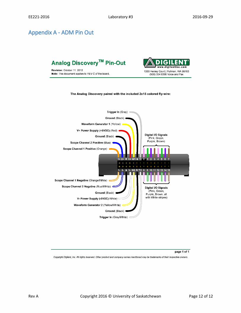
1.1. Use Wavegen Channel 1 (W1, yellow wire, see Appendix A) to generate "Vcc". Set Wavegen to a 80 Hz, 0 to +4 V "triangle" (i.e. Amplitude = 2 V, Offset = 2 V). Also set "Phase" to "90 deg". The Wavegen setting dialog should look similar to Figure 7-2.
Vcc
100 Ω R2
R1
22 kΩ
C
Vbb E
B2N2222A
Q1
Figure 7-1: 2N2222A Circuit Schematic

EE221-2016 Laboratory #3 2016-09-29
Rev A Copyright 2016 © University of Saskatchewan Page 6 of 12
Figure 7-2: AWG1 Settings
1.2. Use Wavegen Channel 2 (W2, yellow-white wire) to generate "Vbb". Use "Select Channels" (highlighted in Figure 7-2) to enable Channel 2. We want Vbb to be 16 voltage steps from 0.25 V to 4 V in 0.25 V steps:
1.2.1. Create a text file with the numbers 1, 2, …, 16, one on each line.
1.2.2. Select the "Custom" waveform type.
1.2.3. Then select "Import" and select the text file you created. "OK" to create the step waveform.
1.2.4. Set Frequency to 10 Hz, Amplitude to 1.875 V, and Offset to 2.125 V.
1.2.5. Set synchronization (to the right of the Channel selector) to "Auto synchronization" which synchronizes Channel 1 and Channel 2.
1.2.6. The Wavegen screen should look similar to Figure 7-3. Note how Channel 1 (Vcc) varies from 0 to 4 V for each voltage step in Channel 2 (Vbb).
1.3. Click "Run All" to start the output from Channel 1 and Channel 2.
2. Connect "Channel 1" (1+ and 1-) to measure the voltage VCE (voltage between Collector and Emitter of the transistor).
3. Connect "Channel 2" (2+ and 2-) to measure the voltage VR2 (voltage across Resistor R2) which we will use to calculate the collector current IC.
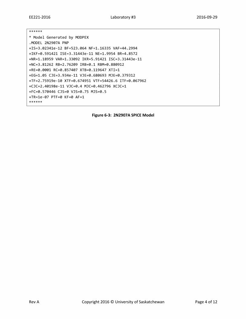
4. Open the Scope window, set “Source:” to “Wavegen 1”, and adjust the scope parameters so that you can see the full pattern of the waveforms. If your circuit is working correctly, you should see

EE221-2016 Laboratory #3 2016-09-29
Rev A Copyright 2016 © University of Saskatchewan Page 7 of 12
something similar to Figure 7-4. Note that the waveforms shown do not make much sense in this mode.
Figure 7-3: Wavegen Settings (both channels)
5. To calculate the collector current IC through the transistor:
5.1. "Add Channel | Custom" and set the function to "C2 / 100". Since this is really a current, change the units to "A".
5.2. Note that there is now an "M1" channel shown in Red in the Scope window. Set the Range on M1 to a more suitable value (e.g. "5 mA/div").
6. To see the I-V Characteristics plot, use "View | Add XY" (set "X: C1" (i.e. VCE) and "Y: M1" (i.e. IC)). Expand the XY window to fill the Scope window as much as possible and adjust "C1" and "M1" to provide a better view of the I-V Characteristics. The screen should look similar to Figure 7-5 (which should be similar to the SPICE simulation). REQUIRED: Demonstrate to a lab instructor and make sure your demonstration is recorded by the lab instructor.
7. Include a screen capture of the I-V Characteristics and annotate on the graph the curves correspond to "Vbb" of 1.0, 2.0, 3.0, and 4.0 V. Also annotate the "Active", "Saturation", and "Cut-off" regions.
8. Change the Vcc waveform into sine wave and square wave to observe (and explain) if there any change in the I-V characteristic display.
EE221-2016 Laboratory #3 2016-09-29
Rev A Copyright 2016 © University of Saskatchewan Page 8 of 12
Figure 7-4: Initial Scope Window
Figure 7-5: Measured 2N2222A I-V Characteristics
9. From the I-V Characteristics curves, what is the apparent value of VCE(saturation)?
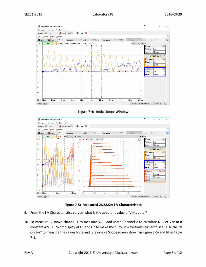
10. To measure IB, move channel 1 to measure VR1. Add Math Channel 2 to calculate IB. Set Vcc to a constant 4 V. Turn off display of C1 and C2 to make the current waveforms easier to see. Use the "X Cursor" to measure the values for IC and IB (example Scope screen shown in Figure 7-6) and fill in Table 7-1.
EE221-2016 Laboratory #3 2016-09-29
Rev A Copyright 2016 © University of Saskatchewan Page 9 of 12
11. Calculate βFdc (i.e. 𝐼𝐼𝐶𝐶 𝐼𝐼𝐵𝐵� ) for each row in Table 7-1. How do these values compare to the value given
in the 2N2222A datasheet?
12. To calculate βFac, for each sample (e.g. "x") use the sample "before" ("x-1") as well as the sample "after" ("x+1"). How do these values compare to the values given in the 2N2222A datasheet?
𝛽𝛽𝐹𝐹𝐹𝐹𝐹𝐹(𝑥𝑥) =
𝐼𝐼𝐶𝐶(𝑥𝑥) − 𝐼𝐼𝐶𝐶(𝑥𝑥 − 1)𝐼𝐼𝐵𝐵(𝑥𝑥) − 𝐼𝐼𝐵𝐵(𝑥𝑥 − 1) + 𝐼𝐼𝐶𝐶(𝑥𝑥 + 1) − 𝐼𝐼𝐶𝐶(𝑥𝑥)
𝐼𝐼𝐵𝐵(𝑥𝑥 + 1) − 𝐼𝐼𝐵𝐵(𝑥𝑥)2
13. Is there any difference between βFdc and βFac? Why might there be a difference?
Figure 7-6: IC and IB Scope Measurement
Vbb (V) IC (mA) IB (µA) βFdc (hFE) βFac (hfe)
0.25
Every 0.25 V until 4 V
Table 7-1: 2N2222A IC versus IB
14. Move Channel 2 to measure VBE. Set the Scope to display IB and VBE (include a screen capture of the Scope window). What appears to be the value of the Base-Emitter Saturation Voltage and how does that compare to the datasheet?

EE221-2016 Laboratory #3 2016-09-29
Rev A Copyright 2016 © University of Saskatchewan Page 10 of 12
2N2907A I-V Characteristics
1. Construct the circuit shown in Figure 7-7 on your breadboard:
1.1. Use Wavegen Channel 1 (W1, yellow wire) to generate "Vcc". Set Channel 1 to a 80 Hz, 0 to –4 V "triangle" (i.e. Amplitude = 2 V, Offset = -2 V). Also set "Phase" to "90 deg".
1.2. Use Wavegen Channel 2 (W2, yellow-white wire) to generate "Vbb". We want Vbb to be 16 voltage steps from -0.25 V to -4 V in 0.25 V steps
Vcc
100 Ω R2
R1
22 kΩ
C
Vbb E
B2N2907A
Q1
Figure 7-7: 2N2907A Circuit Schematic
2. Connect "Channel 1" (1+ and 1-) to measure the voltage VCE (voltage between Collector and Emitter of the transistor).
3. Connect "Channel 2" (2+ and 2-) to measure the voltage VR2 (voltage across Resistor R2) which we will use to calculate the collector current IC.
4. Similar to section 7.2, set up the Scope window to display the I-V Characteristic curves. The screen should look similar to Figure 7-8 (which should be similar to the SPICE simulation). REQUIRED: Demonstrate to a lab instructor and make sure your demonstration is recorded by the lab instructor.
5. Include a screen capture of the I-V Characteristics and annotate on the graph the curves correspond to "Vbb" of -1.0, -2.0, -3.0, and -4.0 V. Also annotate the "Active", "Saturation", and "Cut-off" regions.
6. From the I-V Characteristics curves, what is the apparent value of VCE(saturation)?
7. Similar to section 7.2, calculate βFdc (i.e. 𝐼𝐼𝐶𝐶 𝐼𝐼𝐵𝐵� ) for each row in Table 7-2. How do these values
compare to the values given in the 2N2907A datasheet?
8. Is there any difference between βFdc and βFac? Why might there be a difference?
9. Move the appropriate channels and set the Oscilloscope to display IB and VBE (include a screen capture of the Oscilloscope window). What appears to be the value of the Base-Emitter Saturation Voltage and how does that compare to the datasheet?

EE221-2016 Laboratory #3 2016-09-29
Rev A Copyright 2016 © University of Saskatchewan Page 11 of 12
Figure 7-8: 2N2907A I-V Characteristics
Vbb (V) IC (mA) IB (µA) βFdc (hFE) βFac (hfe)
-0.25
Every 0.25 V until -4 V
Table 7-2: 2N2907A IC versus IB
EE221-2016 Laboratory #3 2016-09-29
Rev A Copyright 2016 © University of Saskatchewan Page 12 of 12
Appendix A - ADM Pin Out