Embed Size (px)
Citation preview
18-545: ADVANCED DIGITAL DESIGN PROJECT
FALL 2015
BRANDON LUCIA
L2: FPGA HARDWARE
18-545: FALL 2014
Admin stuff
Project Proposals happen on Monday Be prepared to give an in-class presentation
Lab 1 is due Wednesday, Sept. 16th
Reading Assignment #1 due today Submit a PDF/text file, don't fill in the web form
Team assignments are done
2
18-545: FALL 2014
Admin Stuff
Status reports due today No word docs, please! Be specific about what happened/is going to happen Talk about what YOU did/will do, not just what your group did Grades on the way, as general feedback
3
18-545: FALL 2014
Game Plan
Overview
Why use FPGAs?
FPGA Internals
4
Caveat: I will use Xilinx specific terminology since that’s the FPGA company you will be using. Beware that other companies use different terms
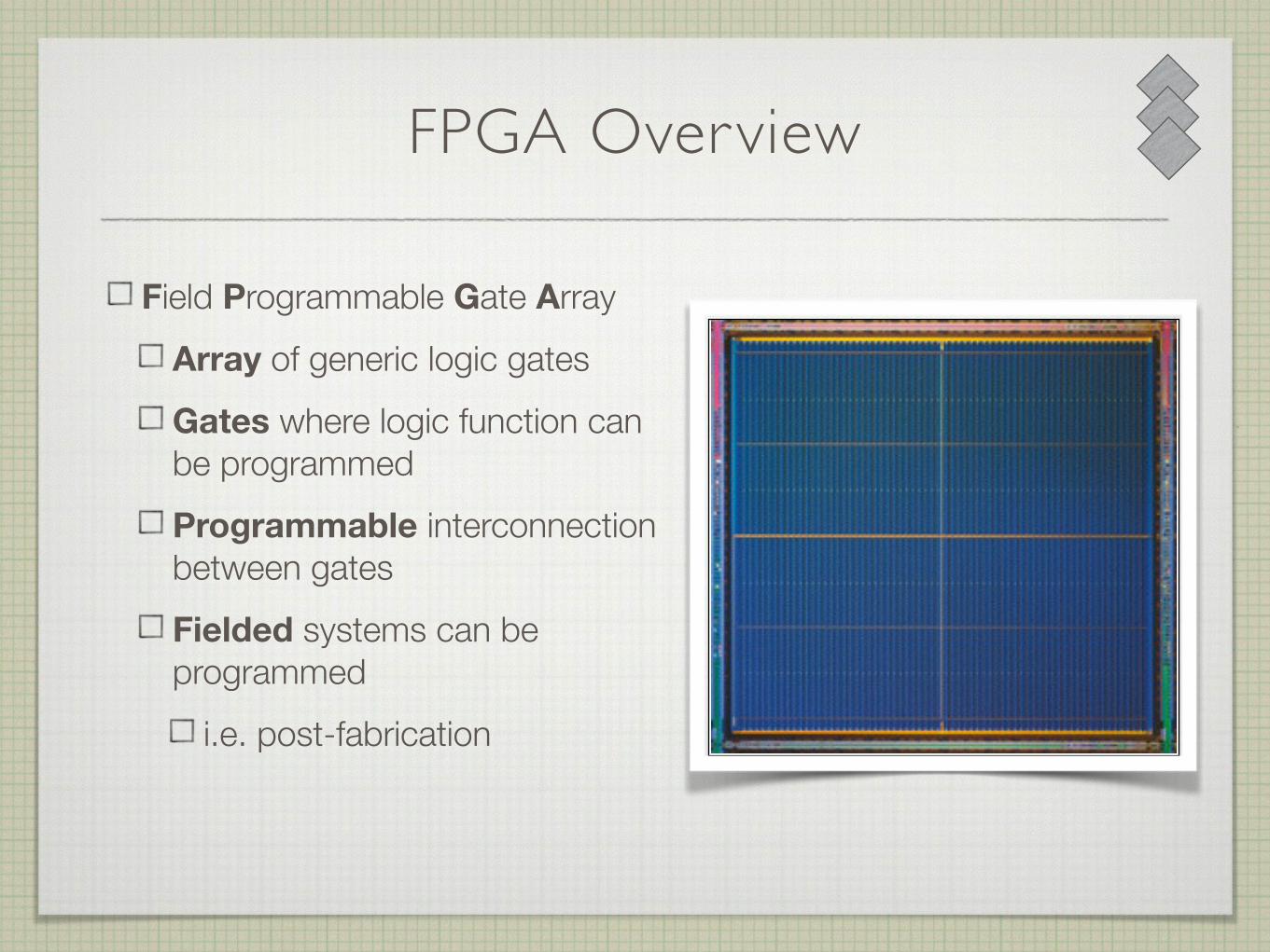
FPGA Overview
Field Programmable Gate Array Array of generic logic gates Gates where logic function can be programmed Programmable interconnection between gates Fielded systems can be programmed
i.e. post-fabrication
18-545: FALL 2014
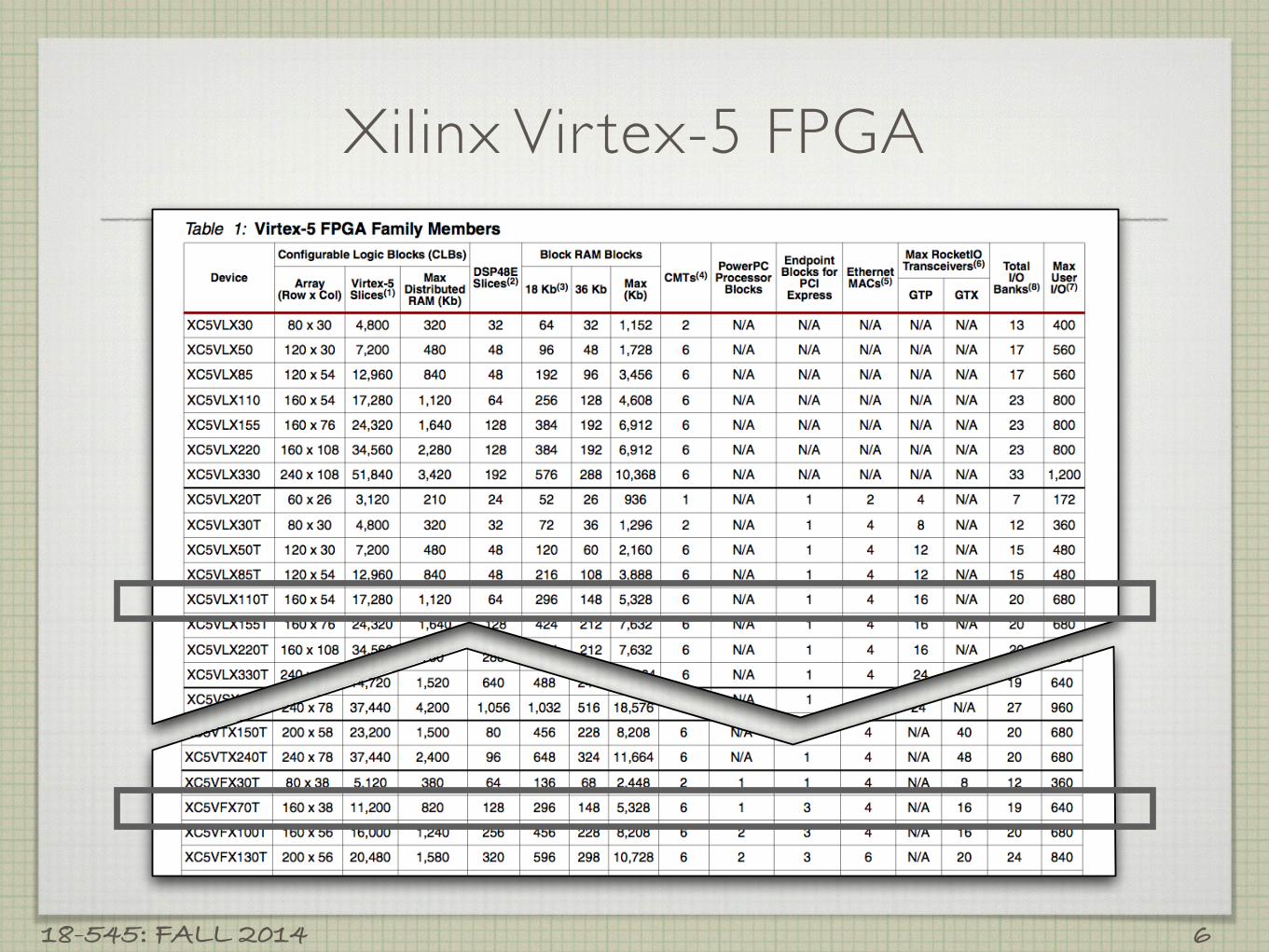
Xilinx Vir tex-5 FPGA
6
18-545: FALL 2014
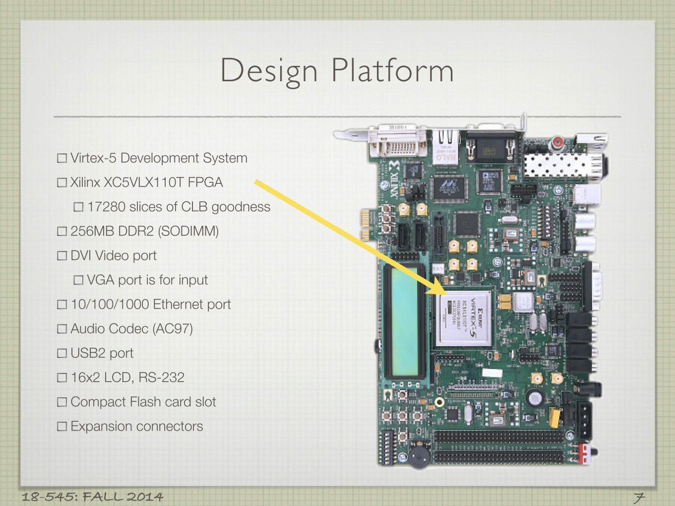
Design Platform
Virtex-5 Development System Xilinx XC5VLX110T FPGA
17280 slices of CLB goodness 256MB DDR2 (SODIMM) DVI Video port
VGA port is for input 10/100/1000 Ethernet port Audio Codec (AC97) USB2 port 16x2 LCD, RS-232 Compact Flash card slot Expansion connectors
7
18-545: FALL 2014
Game Plan
Overview
Why use FPGAs?
FPGA Internals
8
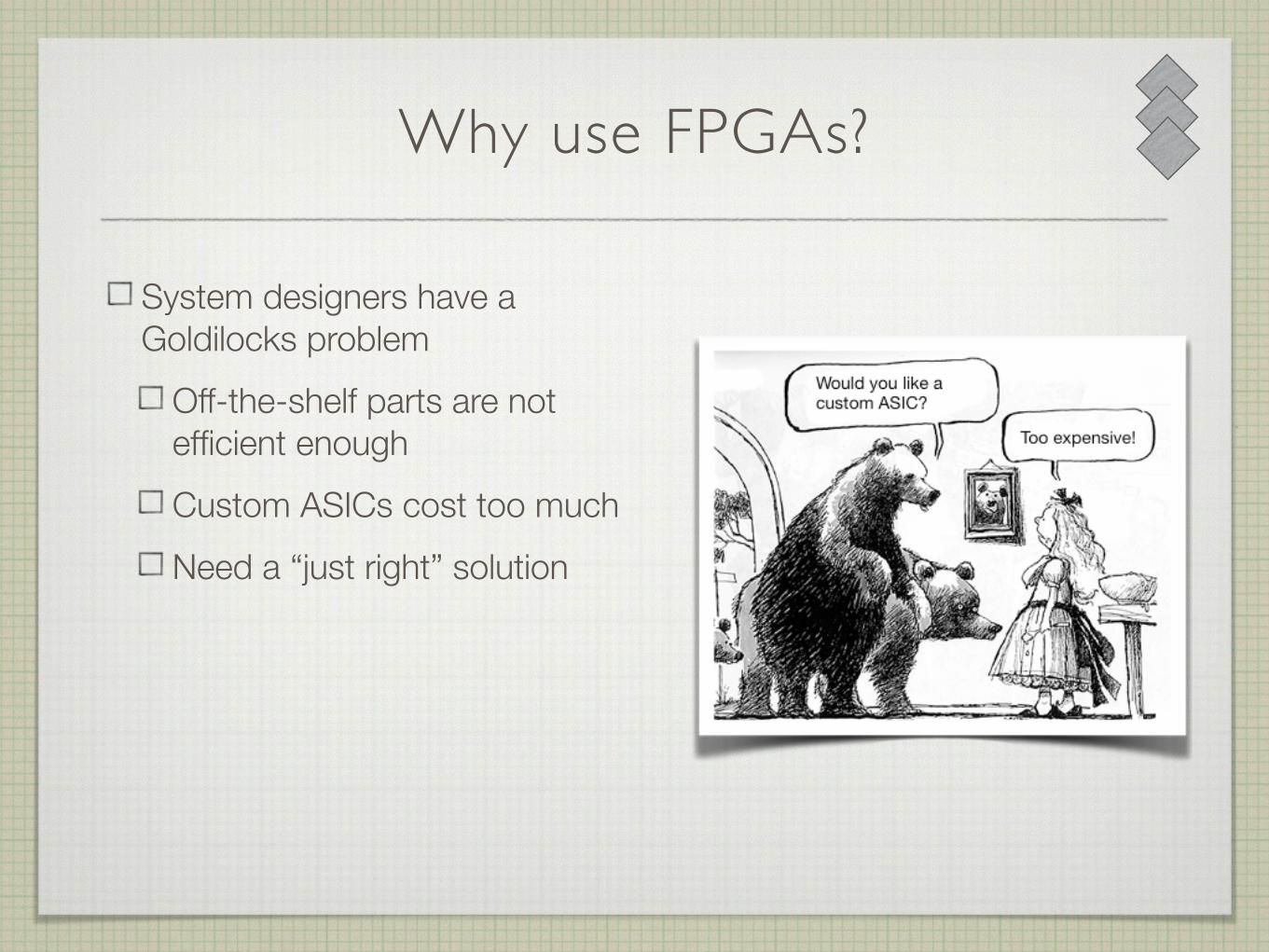
Why use FPGAs?
System designers have a Goldilocks problem
Off-the-shelf parts are not efficient enough Custom ASICs cost too much Need a “just right” solution
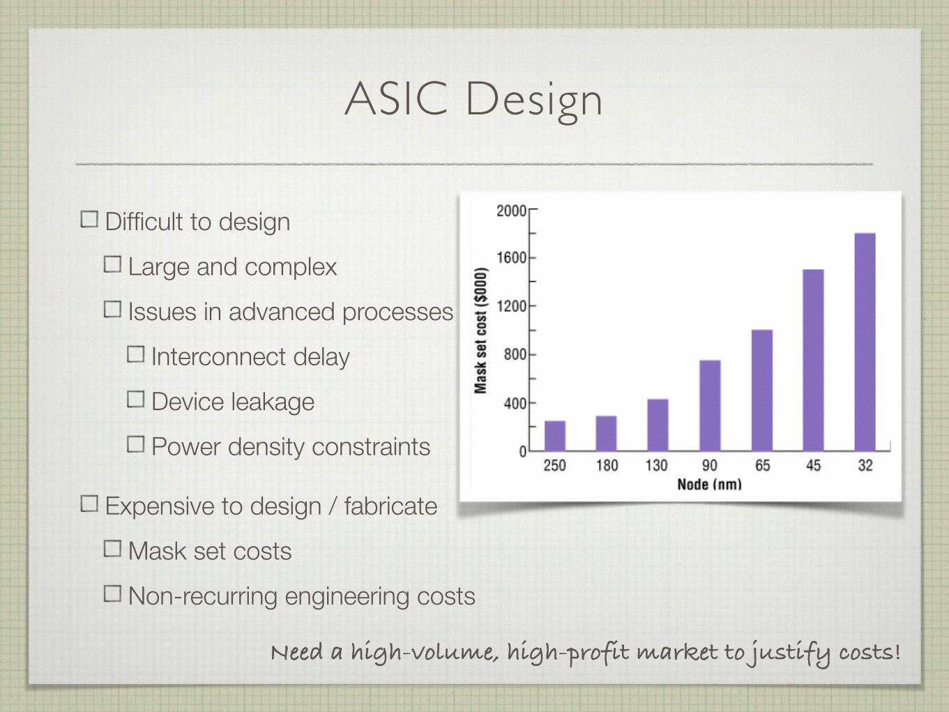
ASIC Design
Difficult to design Large and complex Issues in advanced processes
Interconnect delay Device leakage Power density constraints
Expensive to design / fabricate Mask set costs Non-recurring engineering costs
Need a high-volume, high-profit market to justify costs!
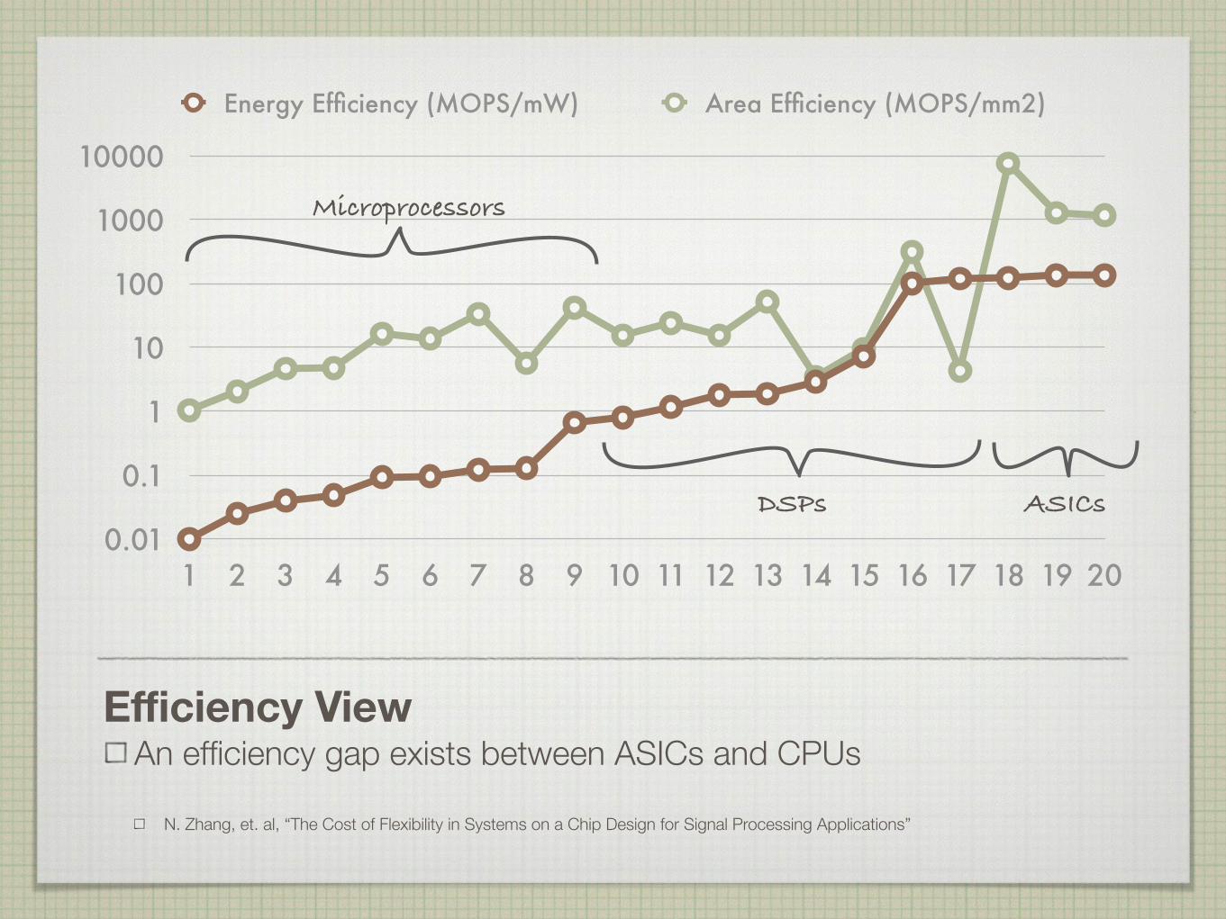
Efficiency View An efficiency gap exists between ASICs and CPUs !N. Zhang, et. al, “The Cost of Flexibility in Systems on a Chip Design for Signal Processing Applications”
0.01
0.1
1
10
100
1000
10000
1 2 3 4 5 6 7 8 9 10 11 12 13 14 15 16 17 18 19 20
Energy Efficiency (MOPS/mW) Area Efficiency (MOPS/mm2)
Microprocessors
ASICsDSPs
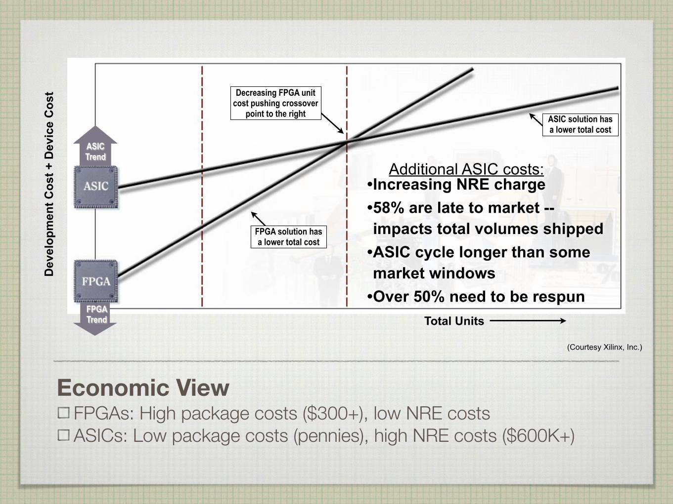
Economic View FPGAs: High package costs ($300+), low NRE costs ASICs: Low package costs (pennies), high NRE costs ($600K+)
Dev
elop
men
t Cos
t + D
evic
e C
ost
•Increasing NRE charge •58% are late to market -- impacts total volumes shipped
•ASIC cycle longer than some market windows
•Over 50% need to be respunTotal Units
Additional ASIC costs:
Decreasing FPGA unit cost pushing crossover
point to the right
ASIC Trend
FPGA Trend
(Courtesy Xilinx, Inc.)
FPGA solution has a lower total cost
ASIC solution has a lower total cost
18-545: FALL 2014
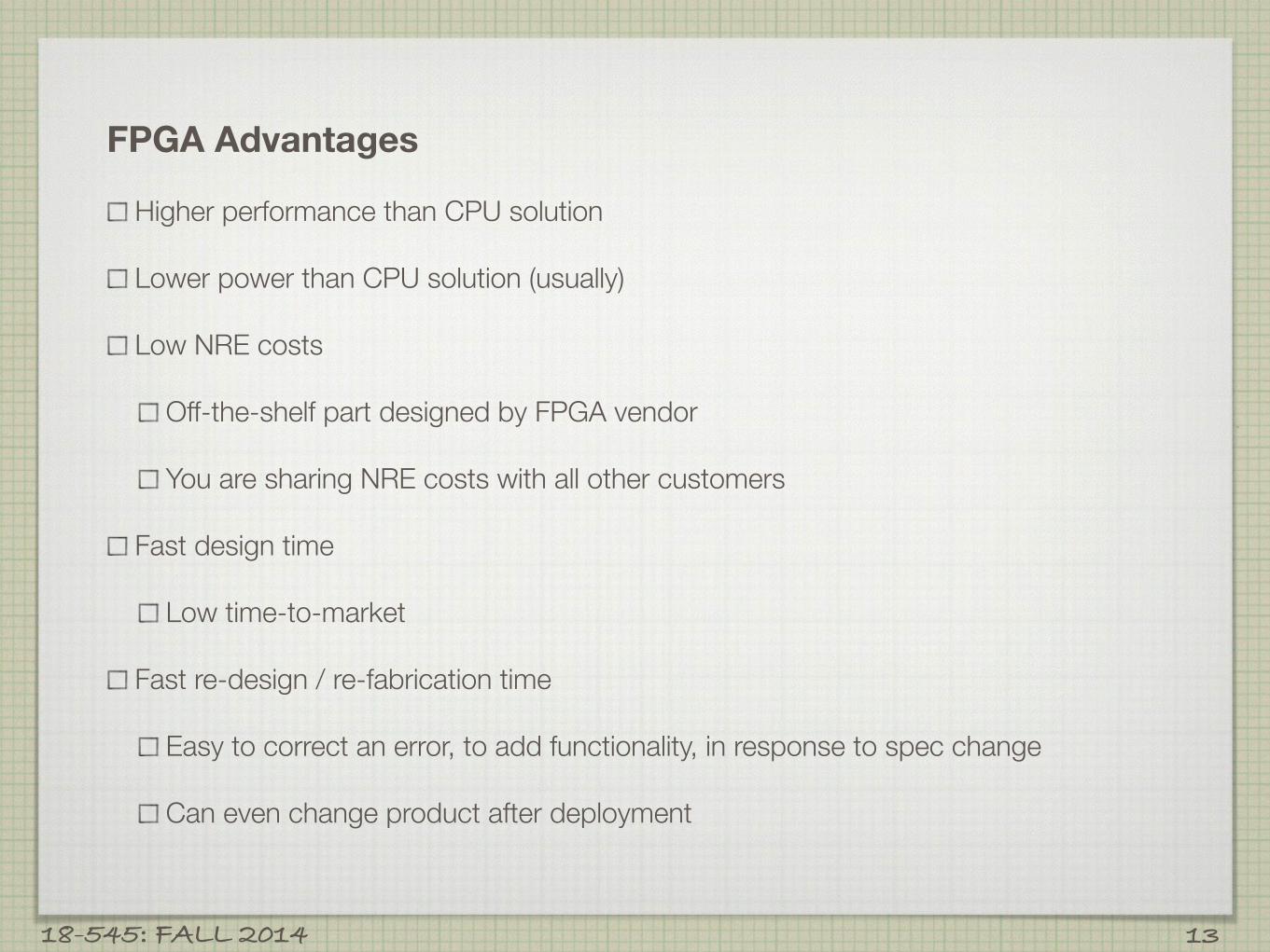
FPGA Advantages
Higher performance than CPU solution
Lower power than CPU solution (usually)
Low NRE costs
Off-the-shelf part designed by FPGA vendor
You are sharing NRE costs with all other customers
Fast design time
Low time-to-market
Fast re-design / re-fabrication time
Easy to correct an error, to add functionality, in response to spec change
Can even change product after deployment
13
18-545: FALL 2014
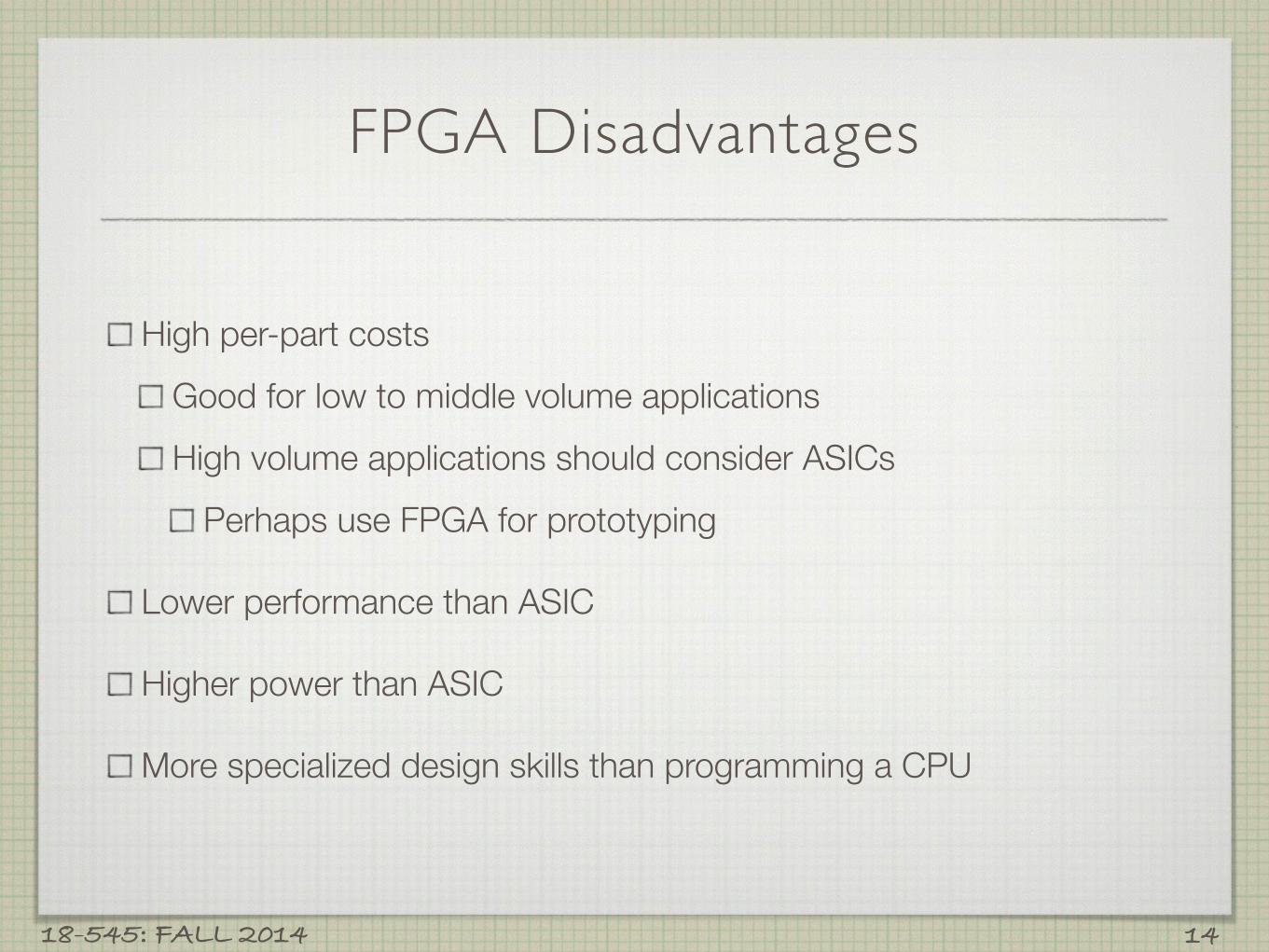
High per-part costs Good for low to middle volume applications High volume applications should consider ASICs
Perhaps use FPGA for prototyping
Lower performance than ASIC
Higher power than ASIC
More specialized design skills than programming a CPU
14
FPGA Disadvantages
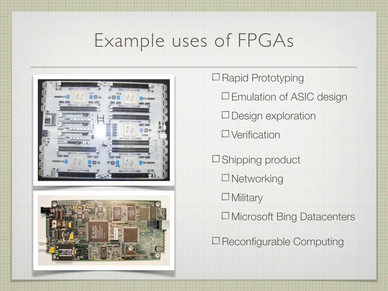
Example uses of FPGAs
Rapid Prototyping Emulation of ASIC design Design exploration Verification
Shipping product Networking Military Microsoft Bing Datacenters
Reconfigurable Computing
18-545: FALL 2014
Game Plan
Overview
Why use FPGAs?
FPGA Internals
16
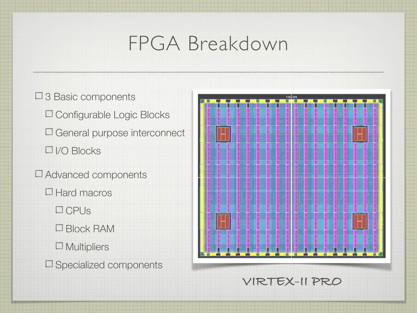
FPGA Breakdown
3 Basic components Configurable Logic Blocks General purpose interconnect I/O Blocks
Advanced components Hard macros
CPUs Block RAM Multipliers
Specialized componentsVIRTEX-II PRO
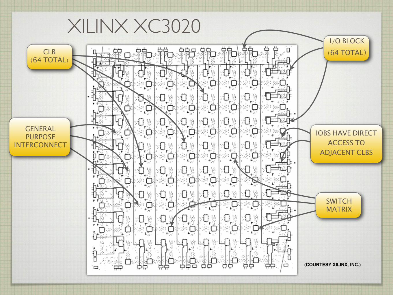
CLB
(64 TOTAL)
I/O BLOCK
(64 TOTAL)
GENERAL
PURPOSE
INTERCONNECTIOBS HAVE DIRECT
ACCESS TO
ADJACENT CLBS
SWITCH
MATRIX
(COURTESY XILINX, INC.)
XILINX XC3020
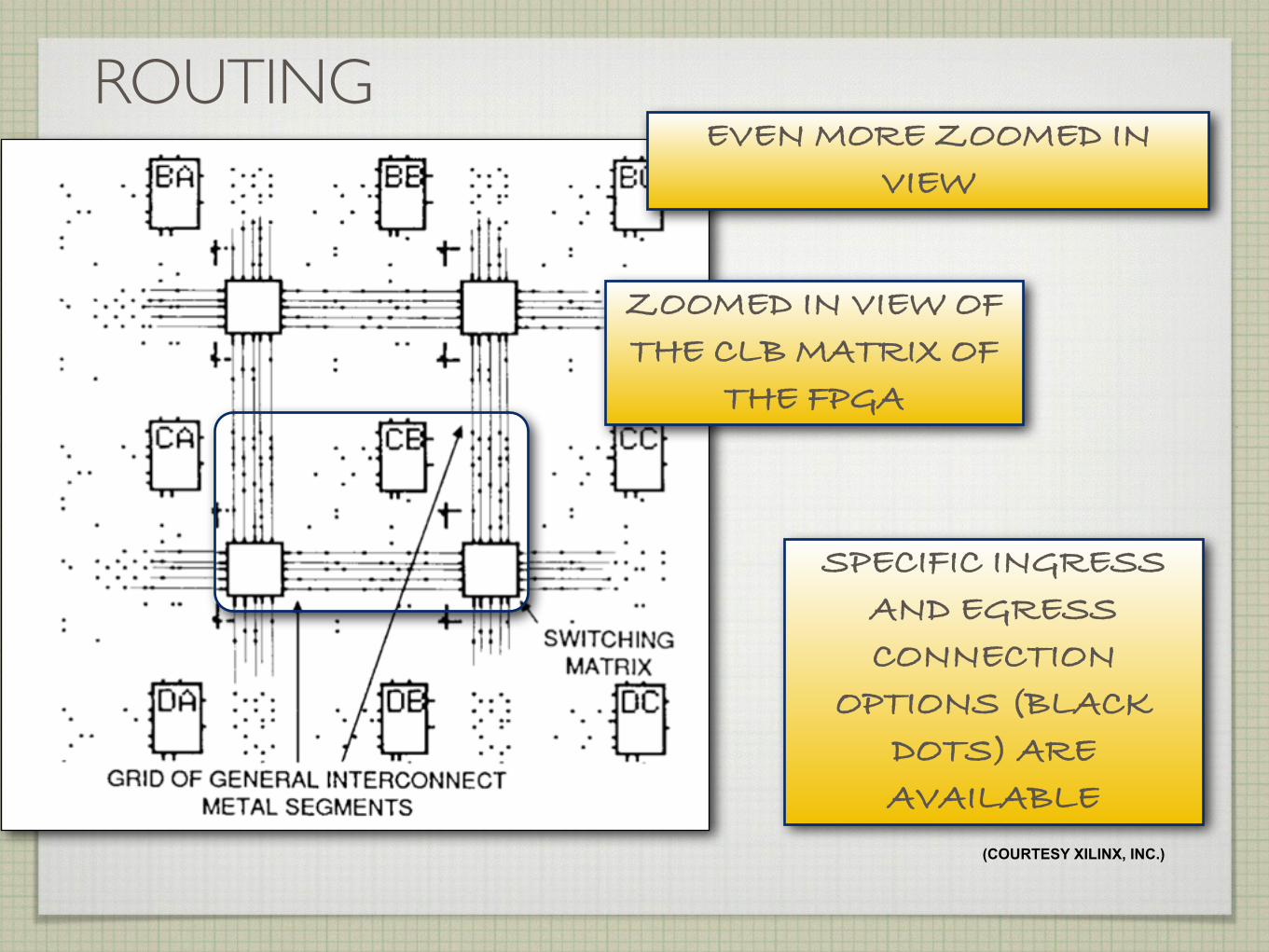
ZOOMED IN VIEW OF THE CLB MATRIX OF
THE FPGA
SPECIFIC INGRESS AND EGRESS CONNECTION
OPTIONS (BLACK DOTS) ARE AVAILABLE
EVEN MORE ZOOMED IN VIEW
(COURTESY XILINX, INC.)
ROUTING
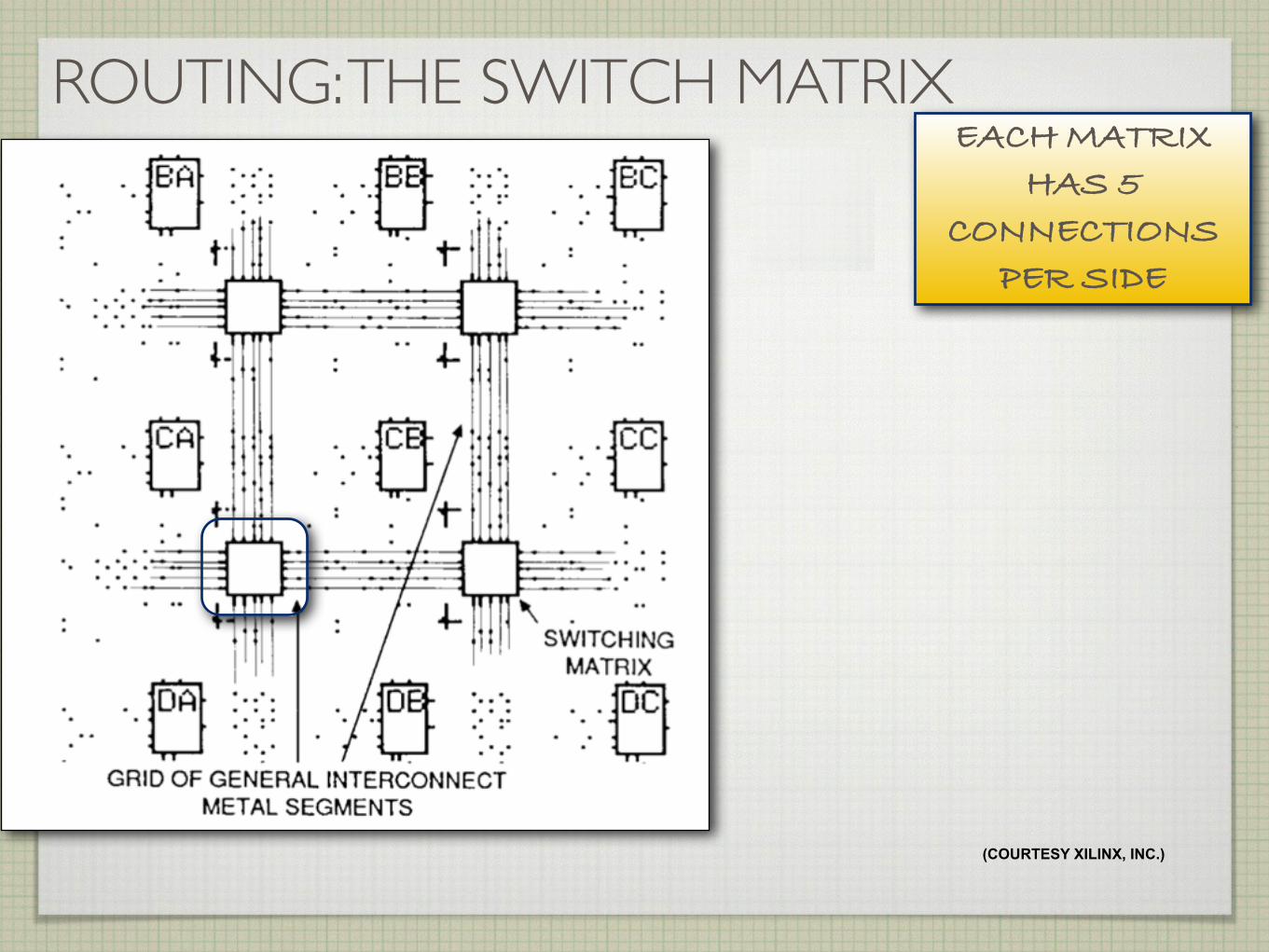
EACH MATRIX HAS 5
CONNECTIONS PER SIDE
(COURTESY XILINX, INC.)
ROUTING: THE SWITCH MATRIX
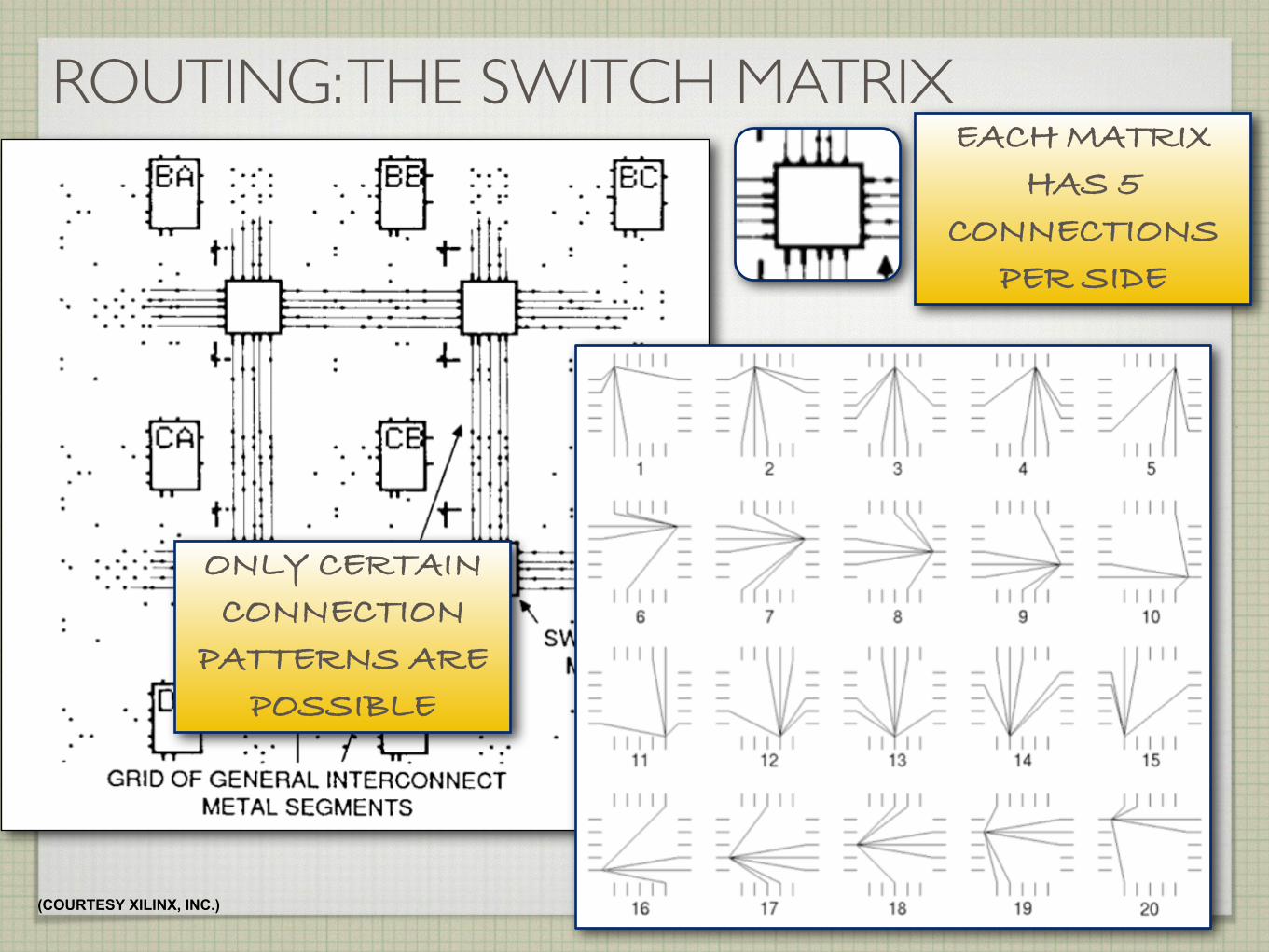
ONLY CERTAIN CONNECTION
PATTERNS ARE POSSIBLE
(COURTESY XILINX, INC.)
ROUTING: THE SWITCH MATRIXEACH MATRIX
HAS 5 CONNECTIONS
PER SIDE
18-545: FALL 2014
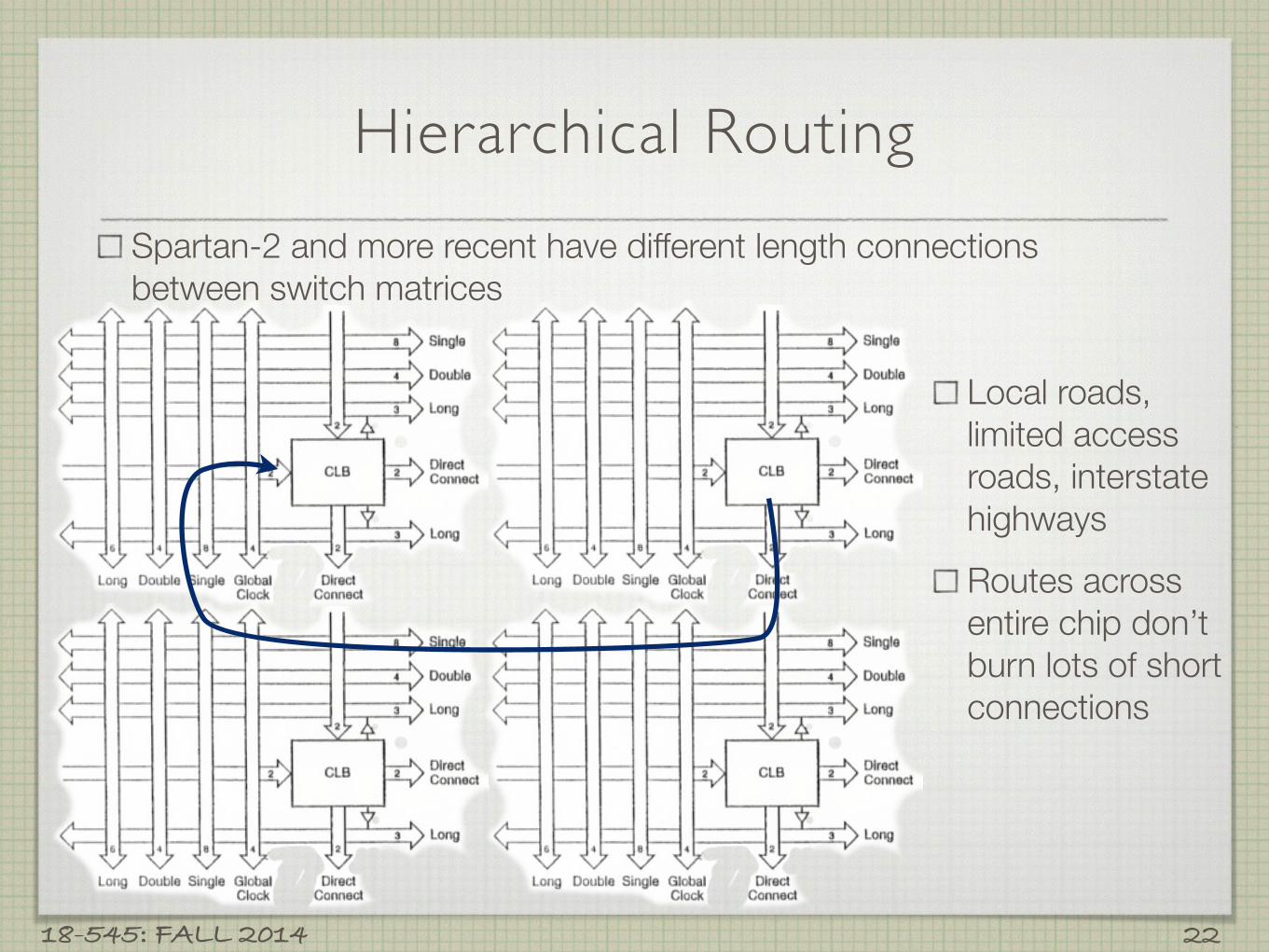
Hierarchical Routing
22
Spartan-2 and more recent have different length connections between switch matrices
Local roads, limited access roads, interstate highways Routes across entire chip don’t burn lots of short connections
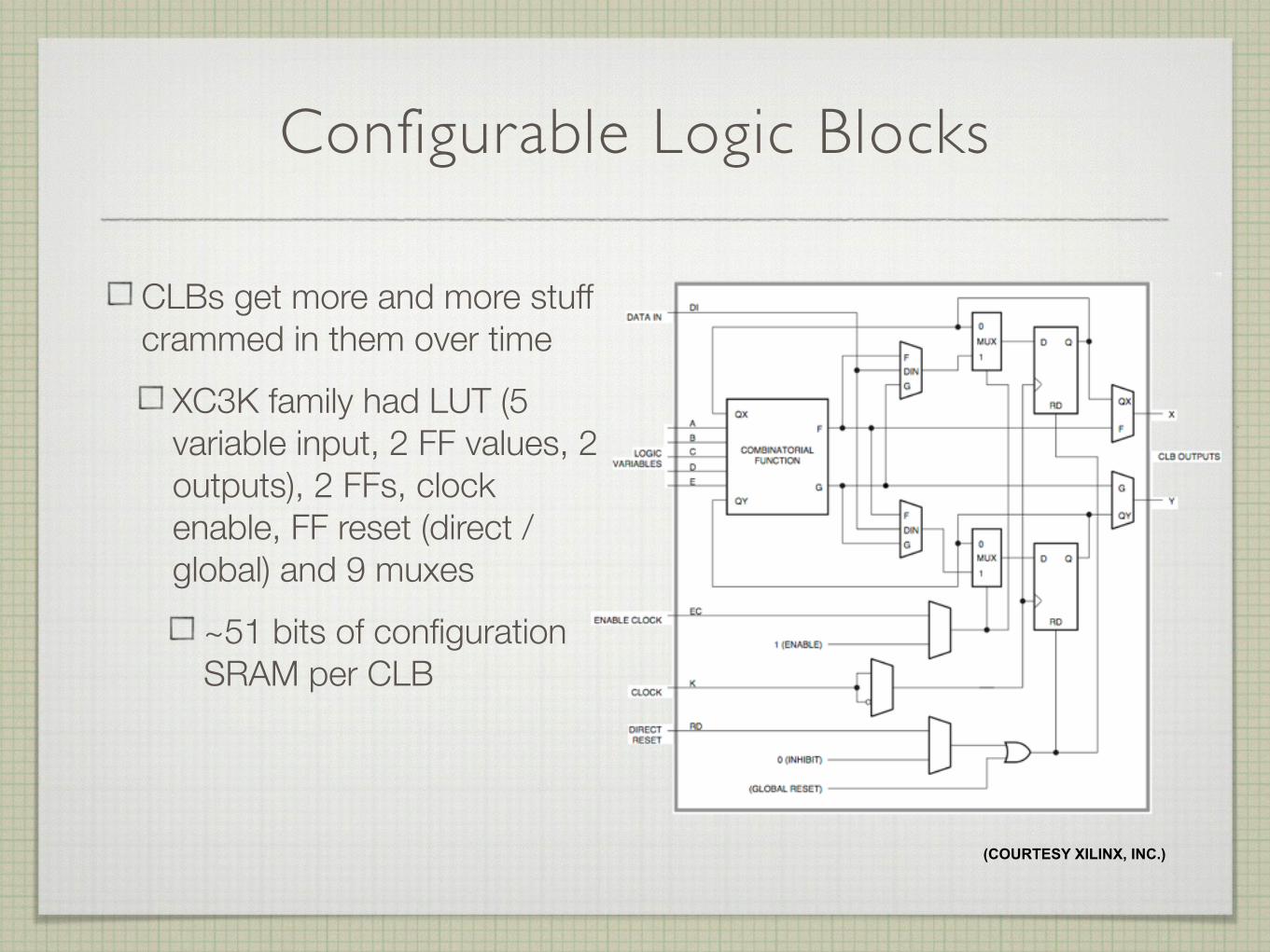
Configurable Logic Blocks
CLBs get more and more stuff crammed in them over time
XC3K family had LUT (5 variable input, 2 FF values, 2 outputs), 2 FFs, clock enable, FF reset (direct / global) and 9 muxes
~51 bits of configuration SRAM per CLB
(COURTESY XILINX, INC.)
18-545: FALL 2014
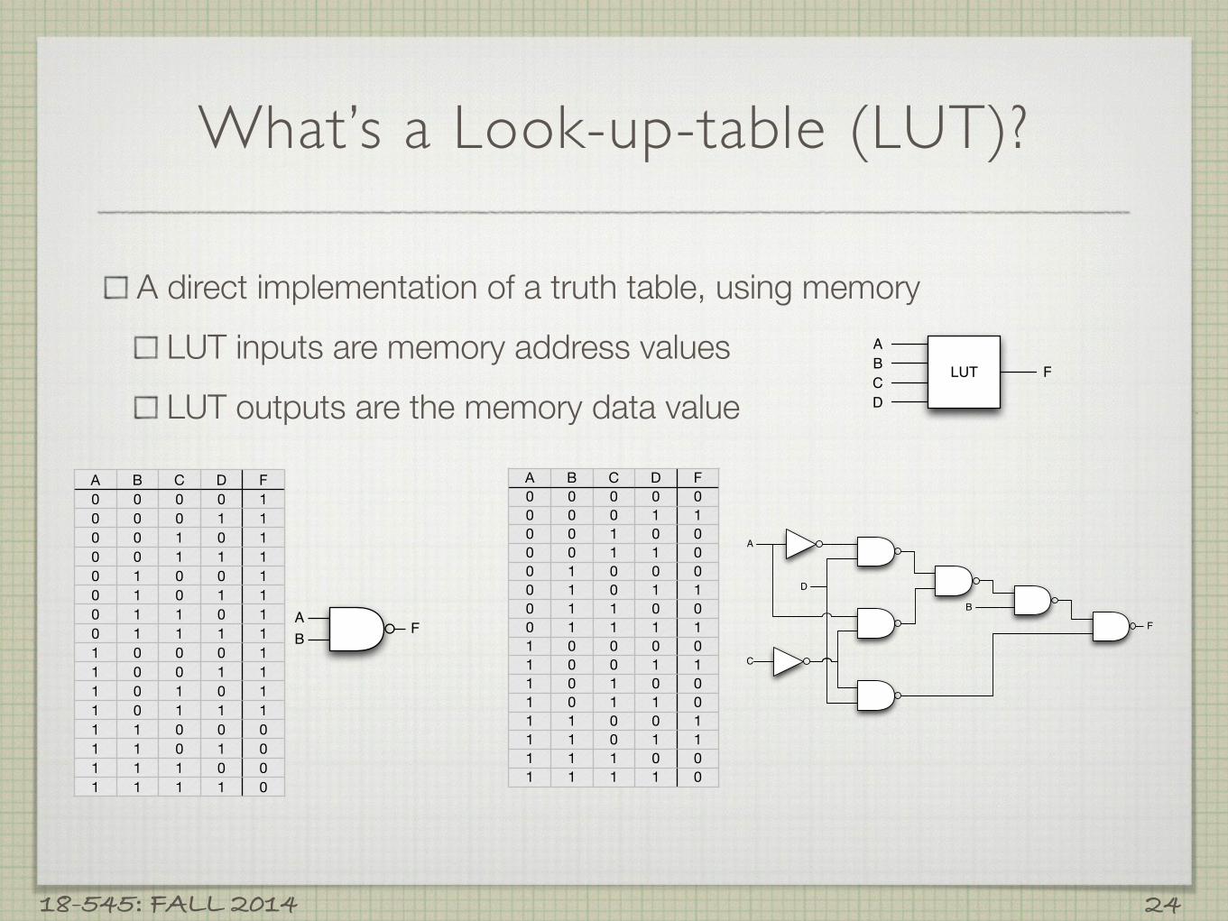
What’s a Look-up-table (LUT)?
A direct implementation of a truth table, using memory LUT inputs are memory address values LUT outputs are the memory data value
24
LUT
ABCD
F
A B C D F0 0 0 0 10 0 0 1 10 0 1 0 10 0 1 1 10 1 0 0 10 1 0 1 10 1 1 0 10 1 1 1 11 0 0 0 11 0 0 1 11 0 1 0 11 0 1 1 11 1 0 0 01 1 0 1 01 1 1 0 01 1 1 1 0
A B C D F0 0 0 0 00 0 0 1 10 0 1 0 00 0 1 1 00 1 0 0 00 1 0 1 10 1 1 0 00 1 1 1 11 0 0 0 01 0 0 1 11 0 1 0 01 0 1 1 01 1 0 0 11 1 0 1 11 1 1 0 01 1 1 1 0
AB
F
A
B
C
D
F
18-545: FALL 2014
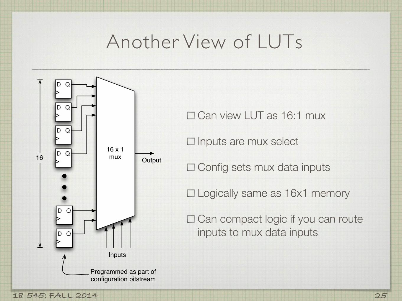
Another View of LUTs
25
D Q
D Q
D Q
D Q
D Q
D Q
16 x 1mux
Inputs
Output16
Programmed as part of configuration bitstream
Can view LUT as 16:1 mux
Inputs are mux select
Config sets mux data inputs
Logically same as 16x1 memory
Can compact logic if you can route inputs to mux data inputs
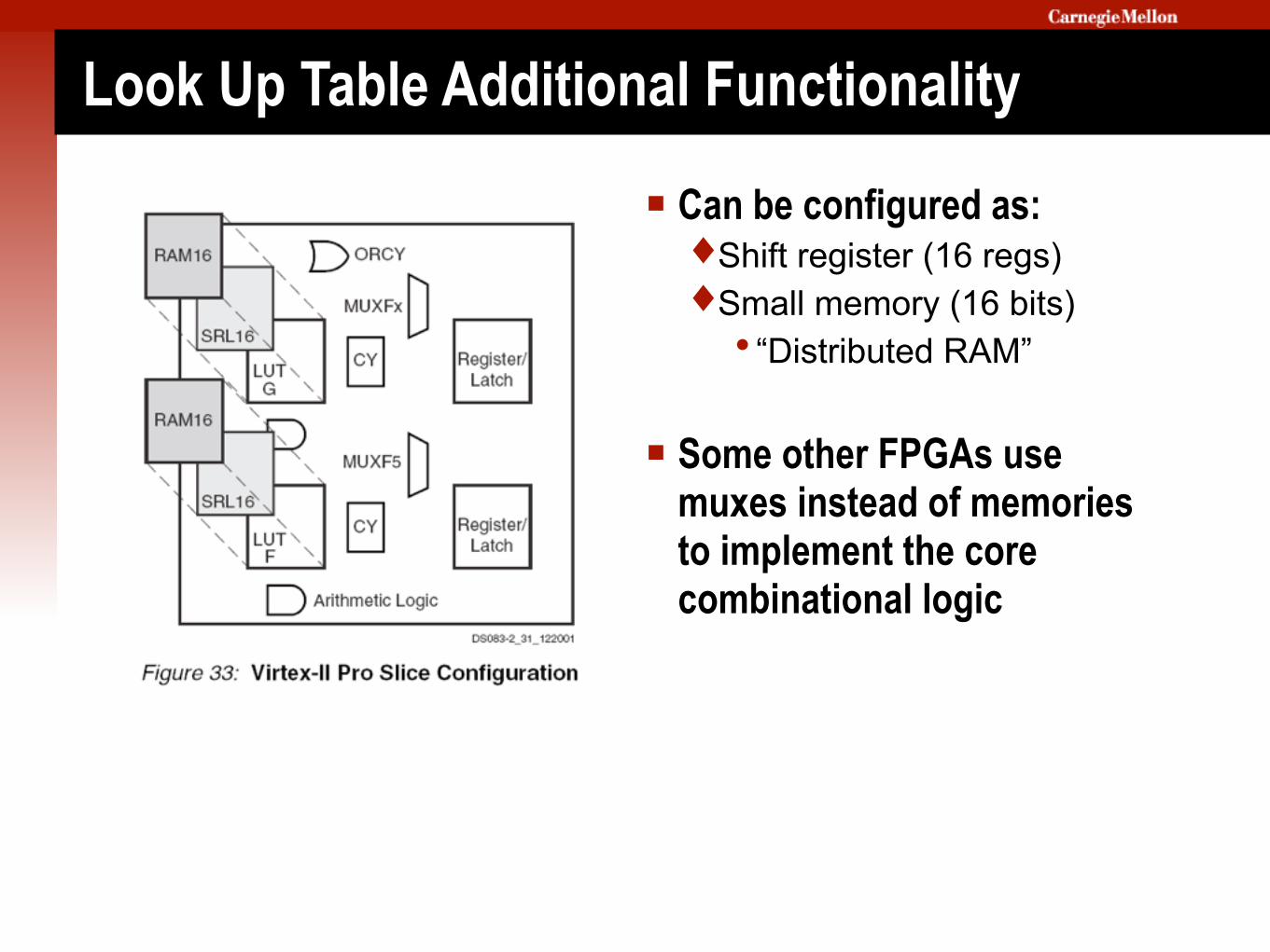
Look Up Table Additional Functionality
§ Can be configured as: ♦Shift register (16 regs) ♦Small memory (16 bits) • “Distributed RAM” !
§ Some other FPGAs use muxes instead of memories to implement the core combinational logic
18-545: FALL 2014
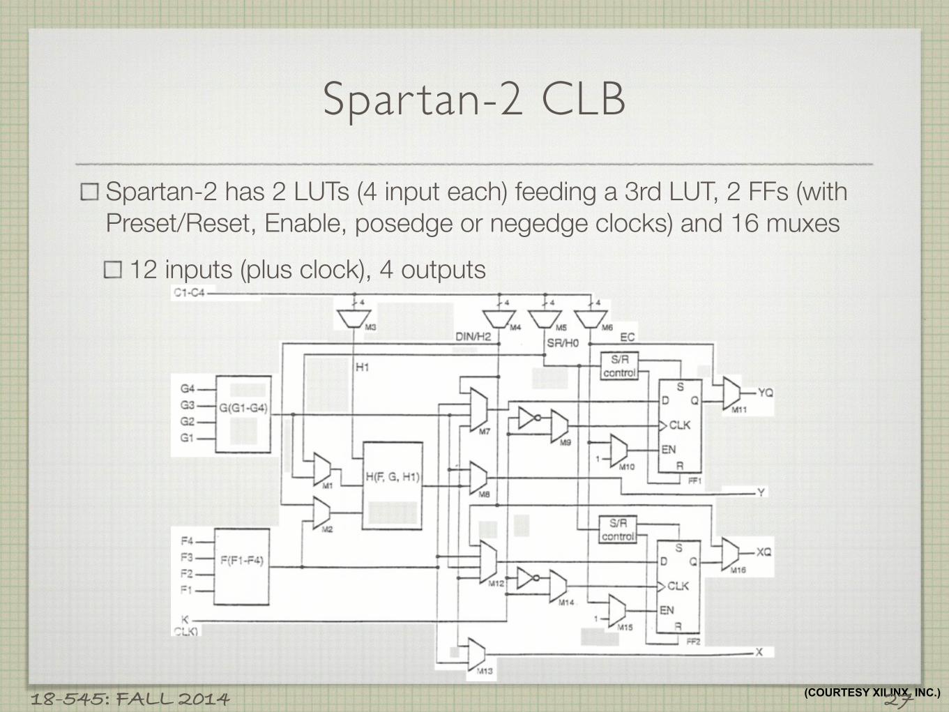
Spar tan-2 CLB
Spartan-2 has 2 LUTs (4 input each) feeding a 3rd LUT, 2 FFs (with Preset/Reset, Enable, posedge or negedge clocks) and 16 muxes
12 inputs (plus clock), 4 outputs
(COURTESY XILINX, INC.)27
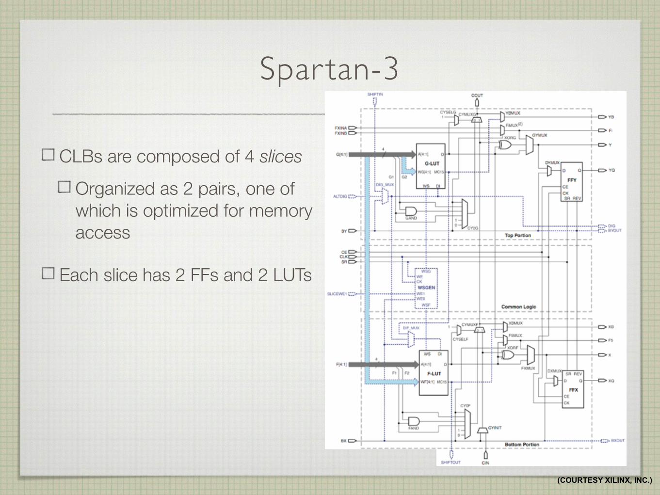
Spar tan-3
CLBs are composed of 4 slices Organized as 2 pairs, one of which is optimized for memory access
Each slice has 2 FFs and 2 LUTs
(COURTESY XILINX, INC.)
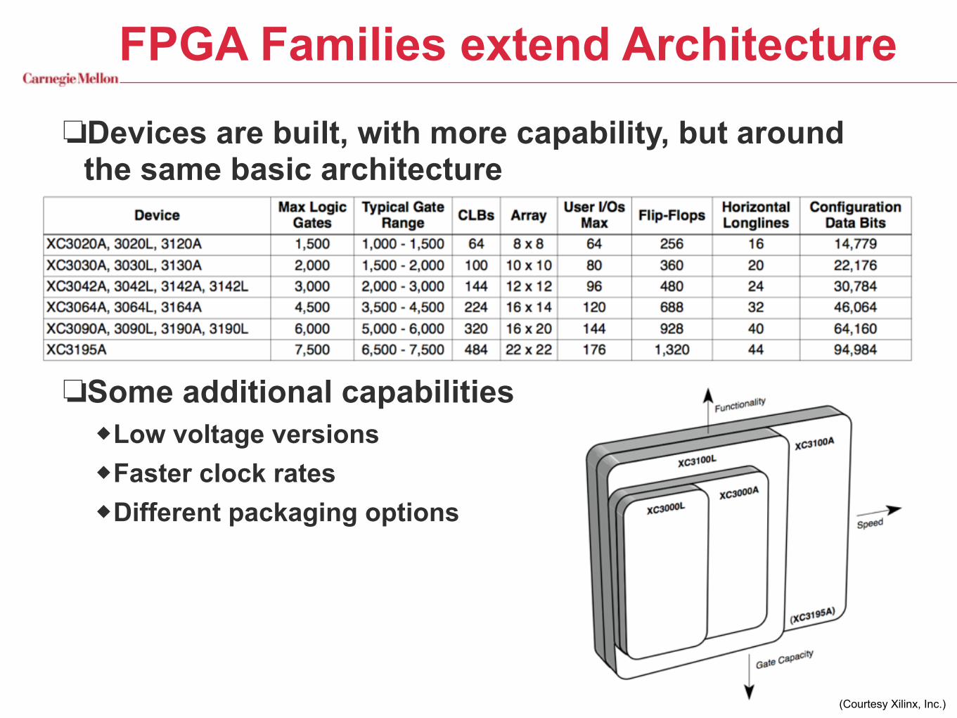
FPGA Families extend Architecture
❏Devices are built, with more capability, but around the same basic architecture
❏Some additional capabilities ◆Low voltage versions ◆Faster clock rates ◆Different packaging options
(Courtesy Xilinx, Inc.)
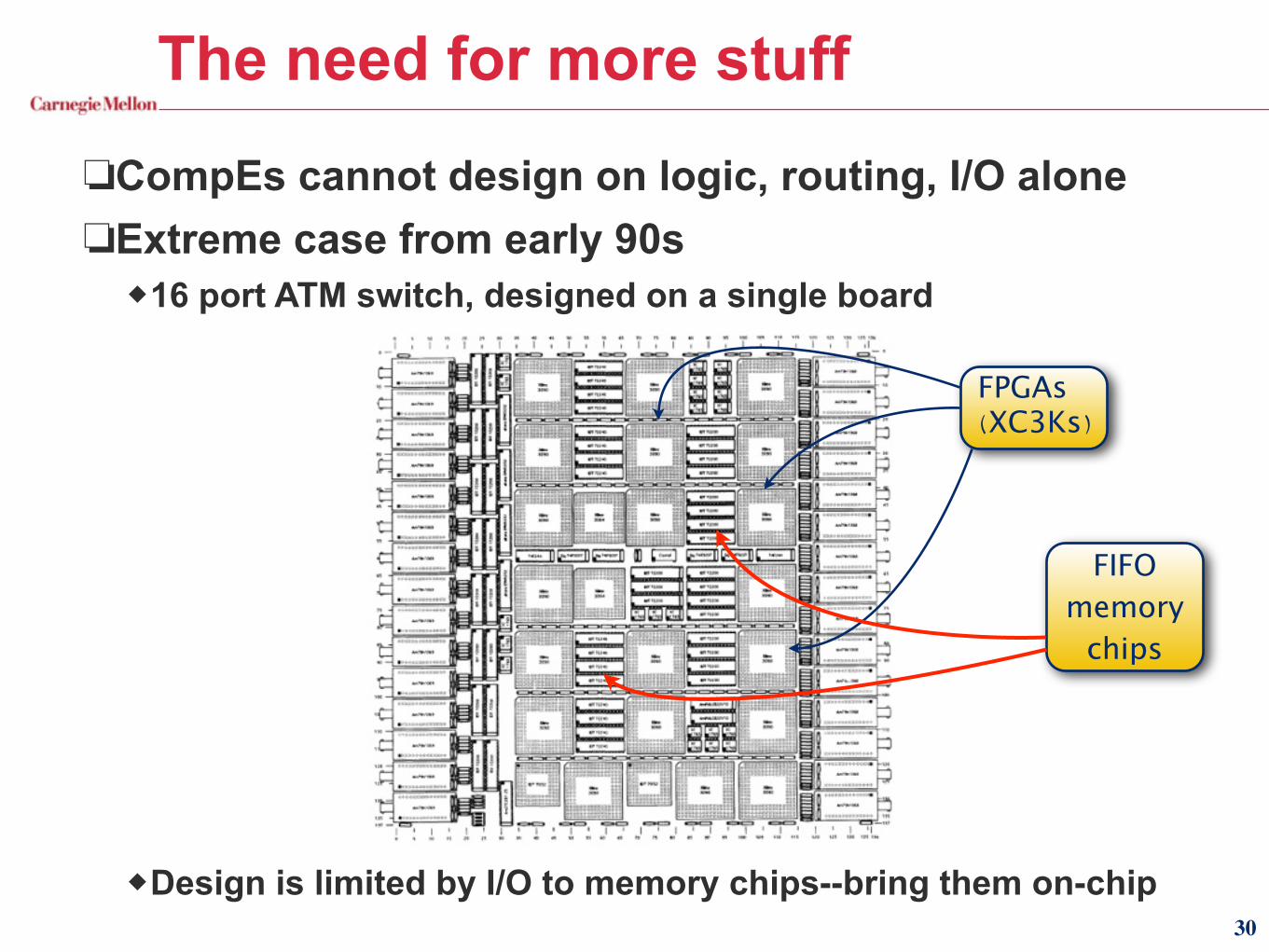
FIFO
memory
chips
The need for more stuff
❏CompEs cannot design on logic, routing, I/O alone ❏Extreme case from early 90s
◆16 port ATM switch, designed on a single board !
◆Design is limited by I/O to memory chips--bring them on-chip
FPGAs (XC3Ks)
30
Other “Stuff”
❏Clock managers ◆Global clock buffering, distribution ◆DCM: eliminate skew, phase shifts, multiply or divide clock
❏Memory ◆Block RAM ◆Distributed RAM (repurposed LUTs)
❏Shift Registers ❏Dedicated Multiplexers ❏Carry Look-Ahead Generators ❏I/O Blocks
◆SelectIO supports 18 standards (single, differential, various voltage levels, ....)
❏Embedded Multipliers31
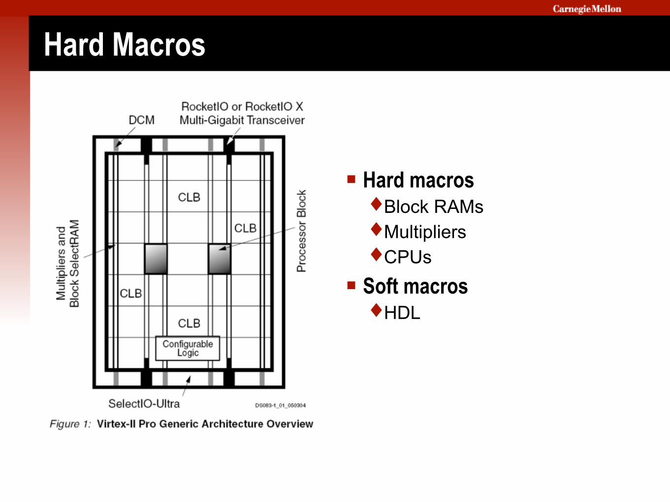
Hard Macros
§ Hard macros ♦Block RAMs ♦Multipliers ♦CPUs
§ Soft macros ♦HDL
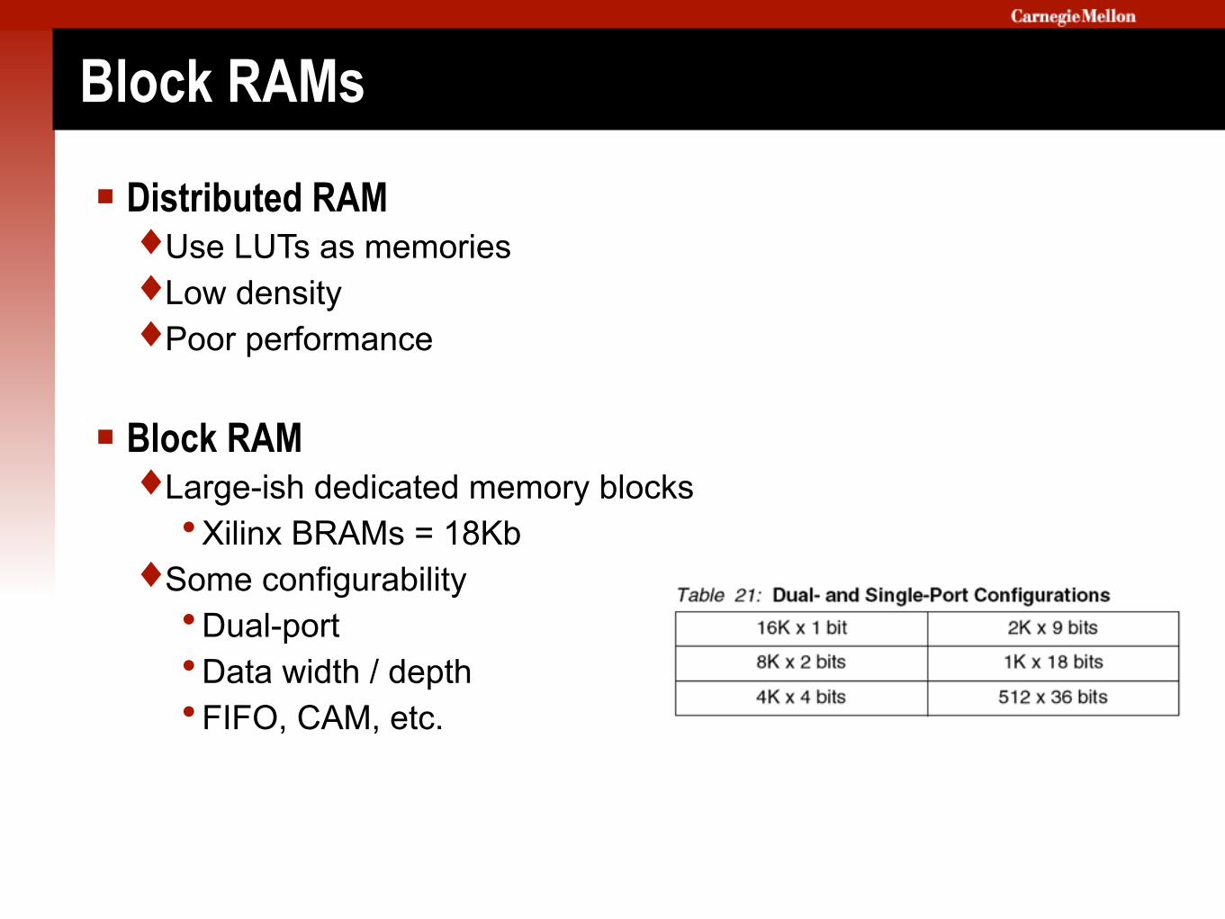
Block RAMs
§ Distributed RAM ♦Use LUTs as memories ♦Low density ♦Poor performance !
§ Block RAM ♦Large-ish dedicated memory blocks •Xilinx BRAMs = 18Kb
♦Some configurability •Dual-port •Data width / depth •FIFO, CAM, etc.
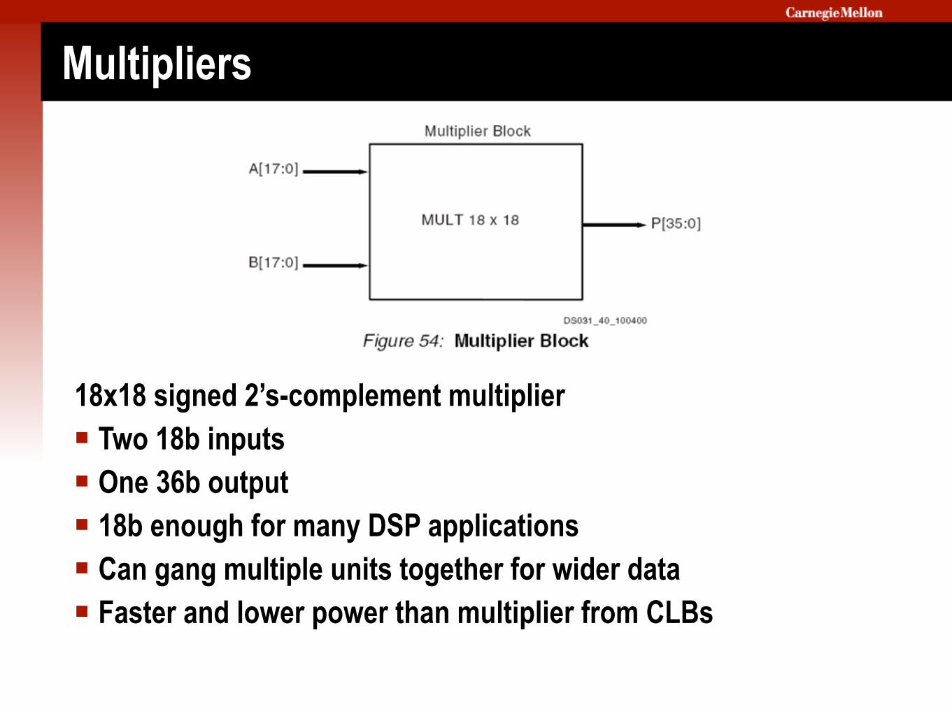
Multipliers
18x18 signed 2’s-complement multiplier § Two 18b inputs § One 36b output § 18b enough for many DSP applications § Can gang multiple units together for wider data § Faster and lower power than multiplier from CLBs
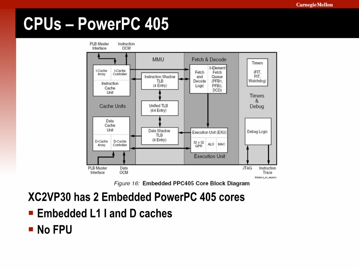
CPUs – PowerPC 405
XC2VP30 has 2 Embedded PowerPC 405 cores § Embedded L1 I and D caches § No FPU
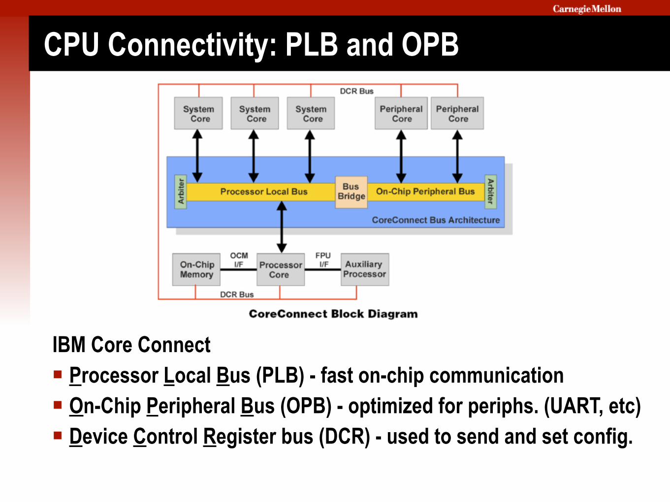
CPU Connectivity: PLB and OPB
IBM Core Connect § Processor Local Bus (PLB) - fast on-chip communication § On-Chip Peripheral Bus (OPB) - optimized for periphs. (UART, etc) § Device Control Register bus (DCR) - used to send and set config.
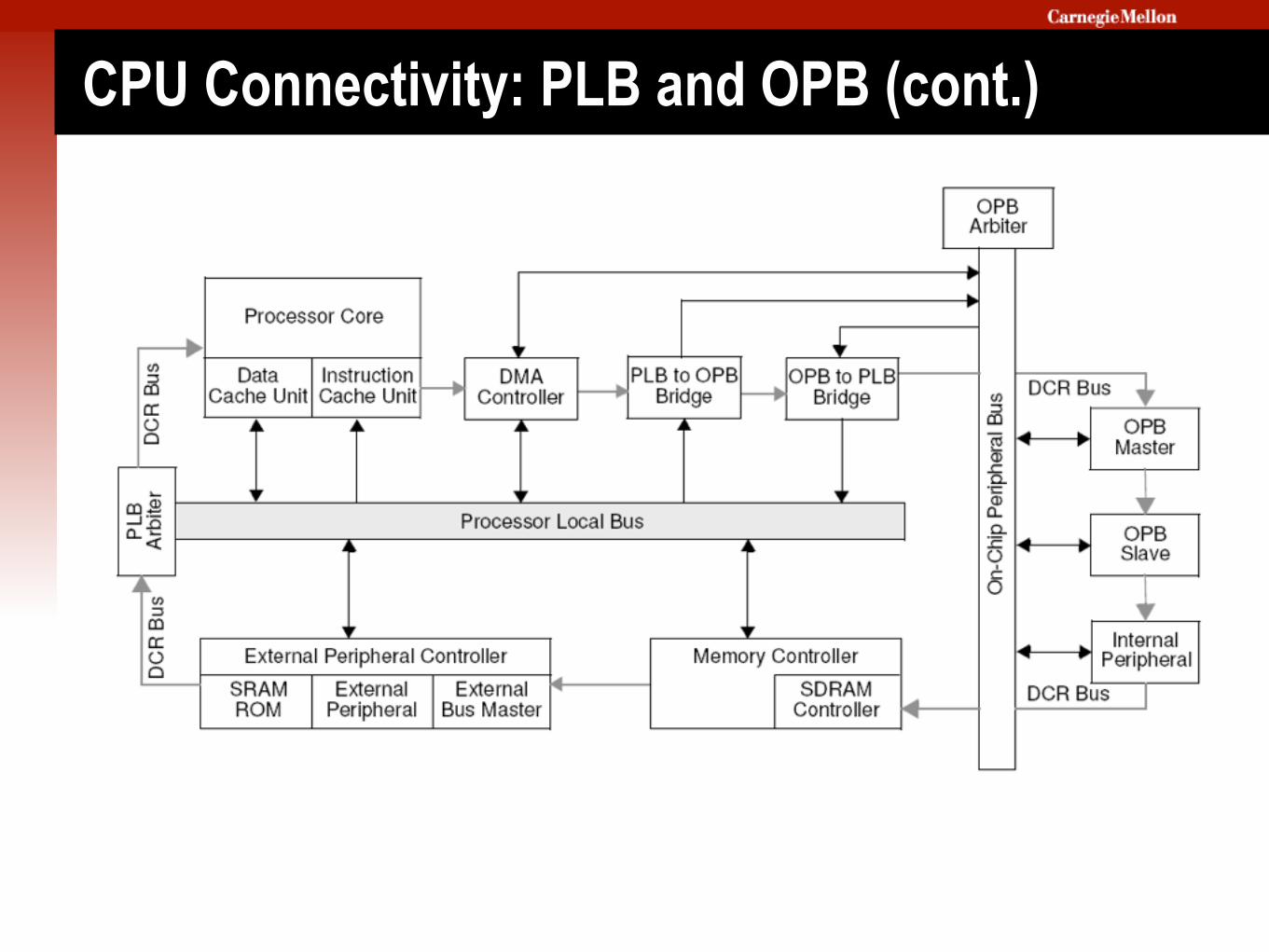
CPU Connectivity: PLB and OPB (cont.)
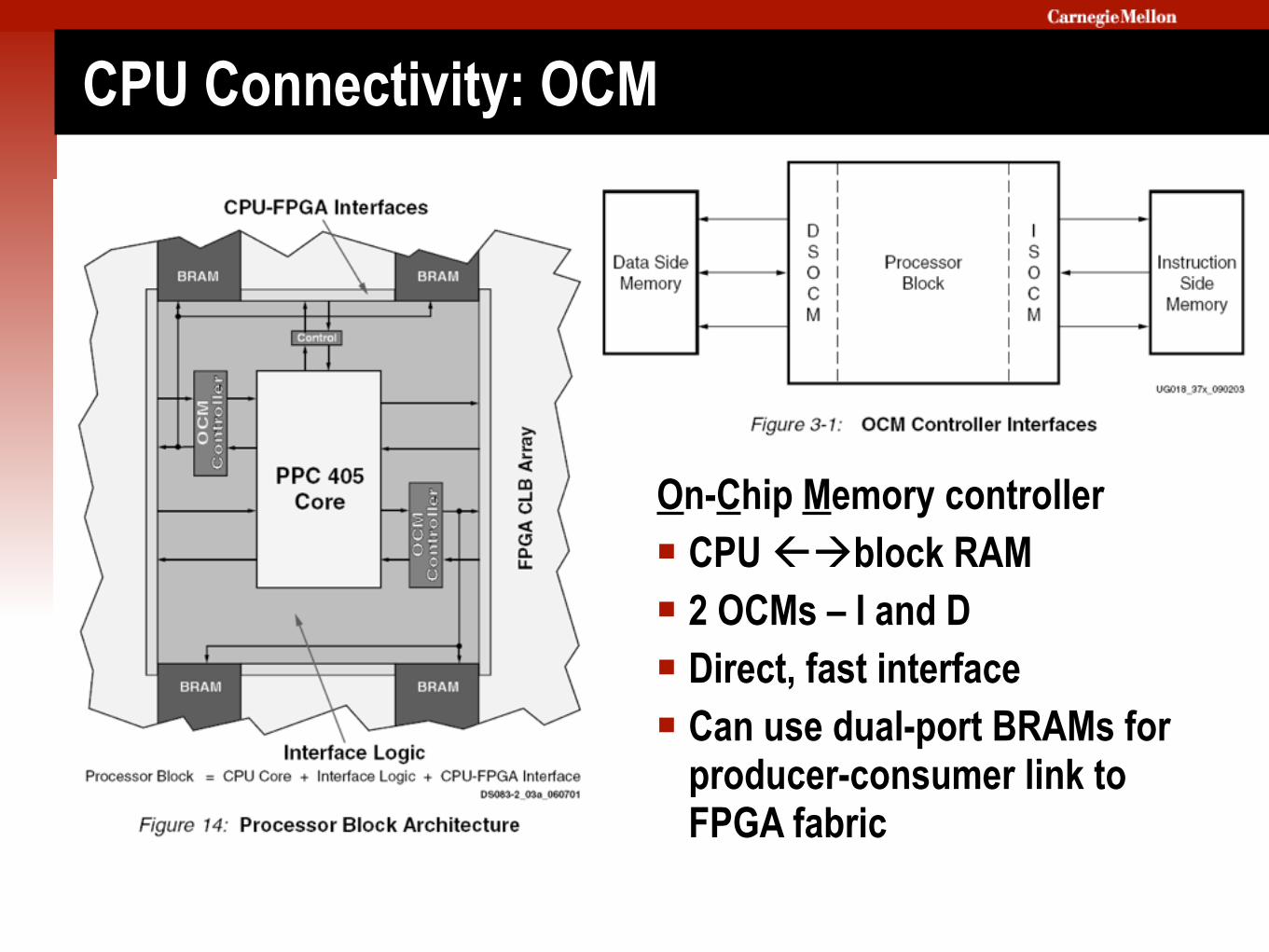
CPU Connectivity: OCM
On-Chip Memory controller § CPU ßàblock RAM § 2 OCMs – I and D § Direct, fast interface § Can use dual-port BRAMs for
producer-consumer link to FPGA fabric
18-545: FALL 2014
CPU Links
A lot more details on the embedded CPU
§ http://www.xilinx.com/bvdocs/userguides/ppc_ref_guide.pdf
§ http://direct.xilinx.com/bvdocs/userguides/ug018.pdf
§ http://www-3.ibm.com/chips/techlib/techlib.nsf/productfamilies/CoreConnect_Bus_Architecture
39
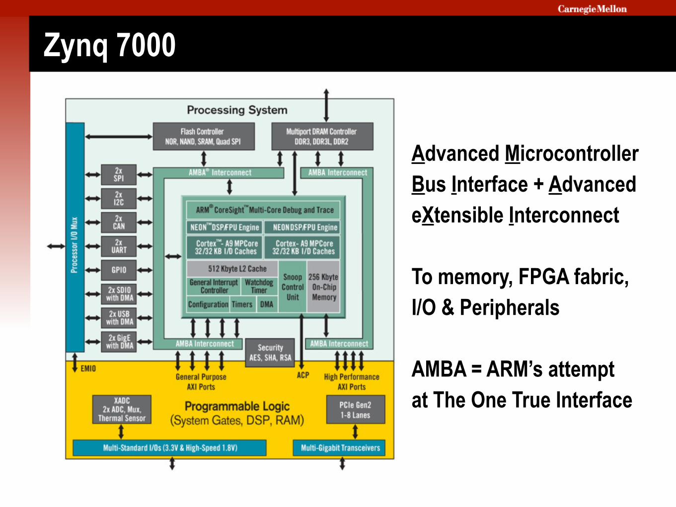
Zynq 7000
Advanced Microcontroller Bus Interface + Advanced eXtensible Interconnect !
To memory, FPGA fabric, I/O & Peripherals !
AMBA = ARM’s attempt at The One True Interface
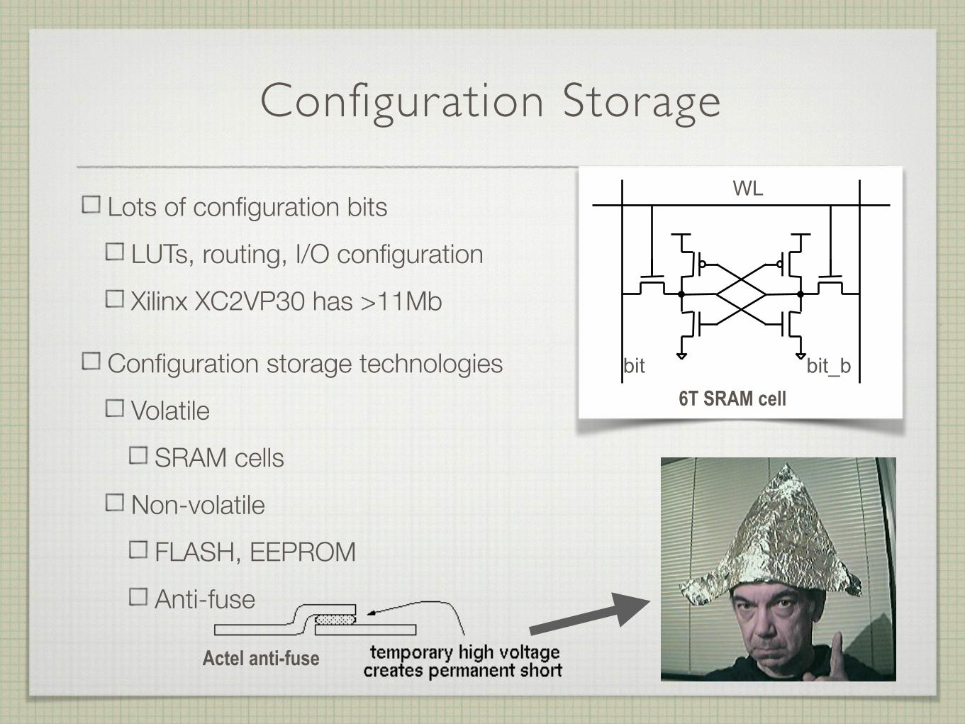
Configuration Storage
Lots of configuration bits LUTs, routing, I/O configuration Xilinx XC2VP30 has >11Mb
Configuration storage technologies Volatile
SRAM cells Non-volatile
FLASH, EEPROM Anti-fuse
Actel anti-fuse
WL
bit bit_b6T SRAM cell
18-545: FALL 2014
Configuration
How to load (scan) configuration bits (bitstream) Connect all configuration registers into single long shift register Serially clock in configuration bits Most designs use standard scan interface (JTAG) developed for test
Bitstream source Non-volatile memory
On-board FLASH, EEPROM, serial memory External media (CF card)
Attached workstation
Can encrypt bitstream to conceal configuration
42
18-545: FALL 2014
Major FPGA Vendors
SRAM-based FPGAs Xilinx Altera Atmel Lattice Semiconductor
Flash & antifuse FPGAs Actel Corp. Quick Logic Corp. Lattice Semiconductor Xilinx (system-in-a-package solution)
Share over 60% of the market
43