Embed Size (px)
Citation preview

© 2005 Panasonic Communications Co., Ltd. Allrights reserved. Unauthorized copying anddistribution is a violation of law.
KX-TCD220SLTKX-TCA122EXTKX-TCA121EXTDigital Cordless Answering SystemTitanium Black Version
(for Switzerland)
Telephone Equipment
ORDER NO. KM40503650CE

1 ABOUT LEAD FREE SOLDER (PbF: Pb free) 4
1.1. Suggested PbF Solder 4
1.2. How to Recognize that Pb Free Solder is Used 5
2 FOR SERVICE TECHNICIANS 5
3 CAUTION 5
4 BATTERY 6
4.1. Battery Installation 6
4.2. Battery Charge 6
4.3. Battery Life 7
4.4. Battery Replacement 7
5 LOCATION OF CONTROLS 8
5.1. Base Unit 8
5.2. Handset 8
6 SETTINGS 9
6.1. Connections 10
6.2. Guide to Settings 11
6.3. Ringer Volume 13
6.4. Night Mode 14
6.5. PIN Code 15
6.6. Reset 16
6.7. Key Lock 17
6.8. R Button to Use the Recall Feature 17
6.9. Pause Button for PBX/Long Distance Service Users 17
6.10. Setting Call Restriction 17
6.11. Turning Call BAR On/Off (Call Prohibition) 18
6.12. Changing the Display Language 18
6.13. Changing the Recall Time 18
6.14. ARS (Automatic Route Selection) 19
7 DISPLAY 20
7.1. Display Icons 20
7.2. Caller ID Display 20
8 OPERATIONS 21
8.1. Turning the Power On/Off 21
8.2. Setting the Date and Time 21
8.3. Redialling 21
8.4. Phonebook 22
8.5. Registering a Handset to a Base Unit 26
8.6. Selecting a Base Unit 27
9 SMS (Short Message Service) 28
9.1. Writing and Sending a New Message 28
9.2. Available Character Entries for SMS 29
9.3. Sending a Saved Message 30
9.4. Editing and Sending a Saved Message 30
9.5. Erasing Saved Messages 30
9.6. Receiving a Message 31
9.7. Reading a Received Message 31
9.8. Replying to a Message 31
9.9. Erasing Received Messages 31
9.10. Changing SMS Message Centre Numbers 32
9.11. Turning SMS On/Off 32
10 Answering System 33
10.1. Turning the Answering System On/Off 33
10.2. Greeting Message 33
10.3. Listening to Message 34
10.4. Using Direct Commands 35
10.5. Remote Operation 36
11 TROUBLESHOOTING 37
12 DISASSEMBLY INSTRUCTIONS 40
12.1. Base Unit 40
12.2. Handset 41
12.3. Charger Unit 42
13 HOW TO REPLACE THE HANDSET LCD 43
14 TROUBLESHOOTING FLOWCHART 44
14.1. Check Power 45
14.2. Check Battery Charge 46
14.3. Check Link 47
14.4. Check Handset Transmission 51
14.5. Check Handset Reception 51
14.6. Check Caller ID 51
14.7. Bell Reception 52
14.8. Check TAM Operation 52
15 TROUBLESHOOTING BY SYMPTOM (BASE UNIT AND
CHARGER UNIT) 53
15.1. Check Point (Base Unit) 53
Note:Because CONTENTS 4 to 11 are the extracts from the Operating Instructions of this model, they are subject to change withoutnotice. Please refer to the original Operating Instructions for further information.
CONTENTS Page Page
2
KX-TCD220SLT / KX-TCA122EXT / KX-TCA121EXT

15.2. The Setting Method of JIG (Base Unit) 57
15.3. Adjustment Standard (Base Unit) 58
15.4. Check Point (Charger Unit) 59
15.5. Adjustment Standard (Charger Unit) 59
16 TROUBLESHOOTING BY SYMPTOM (HANDSET) 60
16.1. Check Point (Handset) 60
16.2. Troubleshooting for Speakerphone 64
16.3. The Setting Method of JIG (Handset) 65
16.4. Adjustment Standard (Handset) 66
17 THINGS TO DO AFTER REPLACING IC 67
17.1. Base Unit 67
17.2. Handset 67
18 RF SPECIFICATION 68
18.1. Base Unit 68
18.2. Handset 68
19 HOW TO CHECK THE HANDSET SPEAKER OR RECEIVER 69
20 FREQUENCY TABLE (MHz) 69
21 BLOCK DIAGRAM (BASE UNIT) 70
22 CIRCUIT OPERATION (BASE UNIT) 71
22.1. Outline 71
22.2. Power Supply Circuit 72
22.3. Telephone Line Interface 73
22.4. Transmitter/Receiver 73
23 BLOCK DIAGRAM (HANDSET) 74
24 CIRCUIT OPERATION (HANDSET) 75
24.1. Outline 75
24.2. Power Supply Circuit/Reset Circuit 75
24.3. Charge Circuit 75
24.4. Battery Low/Power Down Detector 75
24.5. Speakerphone 75
25 CIRCUIT OPERATION (CHARGER UNIT) 76
25.1. Power Supply Circuit 76
26 SIGNAL ROUTE 77
27 CPU DATA (BASE UNIT) 79
27.1. IC8 (BBIC) 79
28 CPU DATA (HANDSET) 81
28.1. IC1 (BBIC) 81
29 ENGINEERING MODE 83
29.1. Base Unit 83
29.2. Handset 86
30 HOW TO REPLACE THE FLAT PACKAGE IC 88
30.1. PREPARATION 88
30.2. FLAT PACKAGE IC REMOVAL PROCEDURE 88
30.3. FLAT PACKAGE IC INSTALLATION PROCEDURE 89
30.4. BRIDGE MODIFICATION PROCEDURE 89
31 CABINET AND ELECTRICAL PARTS LOCATION (BASE UNIT)
90
32 CABINET AND ELECTRICAL PARTS LOCATION (HANDSET) 91
33 CABINET AND ELECTRICAL PARTS LOCATION (CHARGER
UNIT) 92
34 ACCESSORIES AND PACKING MATERIALS 93
34.1. KX-TCD220SLT 93
34.2. KX-TCA121EXT 94
35 TERMINAL GUIDE OF THE ICs, TRANSISTORS AND DIODES
95
35.1. Base Unit 95
35.2. Handset 95
35.3. Charger Unit 95
36 REPLACEMENT PARTS LIST 96
36.1. Base Unit 96
36.2. Handset 98
36.3. Charger Unit 99
36.4. Accessories and Packing Materials 99
36.5. Fixtures and Tools 100
37 FOR SCHEMATIC DIAGRAM 101
37.1. Base Unit (SCHEMATIC DIAGRAM (BASE UNIT)) 101
37.2. Handset (SCHEMATIC DIAGRAM (HANDSET)) 101
37.3. Charger Unit (SCHEMATIC DIAGRAM (CHARGER UNIT))
101
38 SCHEMATIC DIAGRAM (BASE UNIT) 102
39 SCHEMATIC DIAGRAM (HANDSET) 104
40 SCHEMATIC DIAGRAM (CHARGER UNIT) 106
41 CIRCUIT BOARD (BASE UNIT) 107
41.1. Component View 107
41.2. Flow Solder Side View 108
42 CIRCUIT BOARD (HANDSET) 109
42.1. Component View 109
42.2. Flow Solder Side View 110
43 CIRCUIT BOARD (CHARGER UNIT) 111
43.1. Component View 111
43.2. Flow Solder Side View 111
3
KX-TCD220SLT / KX-TCA122EXT / KX-TCA121EXT

1 ABOUT LEAD FREE SOLDER (PbF: Pb free)Note:
In the information below, Pb, the symbol for lead in the periodic table of elements, will refer to standard solder or solder thatcontains lead.
We will use PbF solder when discussing the lead free solder used in our manufacturing process which is made from Tin (Sn),Silver (Ag), and Copper (Cu).
This model, and others like it, manufactured using lead free solder will have PbF stamped on the PCB. For service and repairwork we suggest using the same type of solder although, with some precautions, standard Pb solder can also be used.
Caution
· PbF solder has a melting point that is 50°F ~ 70°F (30°C ~ 40°C) higher than Pb solder. Please use a soldering iron withtemperature control and adjust it to 700°F ± 20°F (370°C ± 10°C). In case of using high temperature soldering iron, pleasebe careful not to heat too long.
· PbF solder will tend to splash if it is heated much higher than its melting point, approximately 1100°F (600°C).
· If you must use Pb solder on a PCB manufactured using PbF solder, remove as much of the original PbF solder as possibleand be sure that any remaining is melted prior to applying the Pb solder.
· When applying PbF solder to double layered boards, please check the component side for excess which may flow onto theopposite side (See the figure below).
1.1. Suggested PbF SolderThere are several types of PbF solder available commercially. While this product is manufactured using Tin, Silver, and Copper(Sn+Ag+Cu), you can also use Tin and Copper (Sn+Cu) or Tin, Zinc, and Bismuth (Sn+Zn+Bi). Please check themanufacturer’s specific instructions for the melting points of their products and any precautions for using their product with othermaterials.
The following lead free (PbF) solder wire sizes are recommended for service of this product: 0.3mm, 0.6mm and 1.0mm.
4
KX-TCD220SLT / KX-TCA122EXT / KX-TCA121EXT

(Example: Handset P.C.B.)
1.2. How to Recognize that Pb Free Solder is Used
C66A201
AN
T
R59
C54
C55
C45
R54 R
55
C46
C47
R62
Q5
Q9
J3
TP
22
CH
GC
HG
TP
23
J2
UT
X
UR
X
J4
C58
C97
C102
C68
C37
C91R
85
C6
C19
R19
R82
C82
SP_TEST1
RE
V_T
ES
T1
RE
V_T
ES
T2
SP_TEST2
C60
C59
C123
C64
C61
C65
C44
C62
CLK
C63
D1
R93
C119
R6
R47
R46
R86
R25
R29
C10
C101
C107
C108
C111
C112
F1
J1 C3
R1
R83R43
C98
L9
L7
L6
C95
C78
C79
VDD3
D7
D6
D9
Q8
D10
C40R5
L5
L4
R74
C80
R36
C76
C16
C92
R80
C13
C83
C69
C70
C81
C86
C15
R35
R67
R66
C14
R34
C75
C38
C77
R61
R71
R40R39
R64
D5
D8
D4
R60
JTAG
R63
VDD1
VDD2POWER
R91
C93
C41
C4
C94
C22
C72
R15
R57
R96
C116
C117
C122
C113
C24
R68
C100
C20C7
R21 R20
BAT GND
C57
C1
C53CN6
C51
C50
C48C49
C67
A
17
26
10
1
C84R75
PbF
IC1IC3
IC2
X1
C21
R90
C18
C96
R92
R72
C99C23
R87
R7
C114R94
C120C115
C71
R89R88
C39
R26C90
C103
R38R37C17
C109C87C12
L1
R12
R81C
118
C104 C
5
C8
Q4
Q11
Q2
Q3
Q10
Q1
Q7
PQUP11278Z
1
1
1
8
8
4
4
5
5
20
80
61
60 41
21
40
Marked
(Component View)
Note:
The location of the “PbF” mark is subject to change without notice.
2 FOR SERVICE TECHNICIANSICs and LSIs are vulnerable to static electricity.
When repairing, the following precautions will help prevent recurring malfunctions.
1. Cover the plastic parts boxes with aluminum foil and ground them.
2. Ground the soldering irons.
3. Use a conductive mat on the worktable.
4. Do not touch IC or LSI pins with bare fingers.
3 CAUTION 1. Danger of explosion if battery is incorrectly replaced.
2. Replace only with the same or equivalent type recommended by the manufacturer.
3. Dispose of used batteries according to the manufacture’s Instructions.
5
KX-TCD220SLT / KX-TCA122EXT / KX-TCA121EXT

4 BATTERY
4.1. Battery Installation 1. Insert the batteries negative ( ) terminal first.
2. Close the handset cover.
Note:
· Use only rechargeable Ni-MH batteries P03P (HHR-4EPT).
4.2. Battery ChargePlace the handset on the base unit for about 7 hours before initial use.
When charging, the battery icon is shown as follows. When the batteries are fully charged, remains on the display.
Note:
· It is normal for the handset to feel warm during charging.
· It takes 7 hours to fully charge the batteries, however, you can use the handset before the batteries are fully charged.
· Clean the charge contacts of the handset and base unit with a soft, dry cloth, otherwise the batteries may not chargeproperly. Clean if the unit is exposed to grease, dust or high humidity.
· When flashes, recharge the handset batteries. will continue to flash until the batteries have been charged for atleast 15 minutes.
· If the handset is turned off, it will be turned on automatically when it is placed on the base unit.
6
KX-TCD220SLT / KX-TCA122EXT / KX-TCA121EXT

4.3. Battery LifeAfter your Panasonic batteries are fully charged, you can expect the following performance:
Ni-MH batteries (700 mAh)
Operation Operating TimeWhile in use (talking) 20 hours max.
While not in use (standby) 170 hours max.
Note:
· Actual battery performance depends on a combination of how often the handset is in use (talking) and how often it is notin use (standby).
· Battery operating time may be shortened over time depending on usage conditions and ambient temperature.
4.4. Battery ReplacementIf flashes even after the handset batteries have been charged for 7 hours, the batteries must be replaced.
Important:
· We recommend the use of Panasonic rechargeable Ni-MH batteries P03P (HHR-4EPT). If you install non-rechargeablebatteries and start charging, the batteries may leak electrolyte.
· Do not mix old and new batteries.
1. Press the notch on the handset cover firmly and slide it in the direction of the arrow.
2. Remove the old batteries positive ( ) terminal first and install the new ones.
Note for Service:
· You could use other rechargeable batteries on sale, but the unit is not guaranteed to work properly.
7
KX-TCD220SLT / KX-TCA122EXT / KX-TCA121EXT

5 LOCATION OF CONTROLS
5.1. Base Unit
5.2. Handset
Note:
· Up to 3 menu items can be displayed at a time. To select a menu item not shown on the current page, scroll up or downby pressing the navigator key, or , respectively.
8
KX-TCD220SLT / KX-TCA122EXT / KX-TCA121EXT

6 SETTINGSImportant Information
General
· Use only the AC adaptor included with this product.
· Do not connect the AC adaptor to any AC outlet other than a standard 220 - 240 V AC outlet.
· This product is unable to make calls when:
− − − − The portable handset battery(ies) need recharging or have failed.
− − − − There is a power failure.
− − − − The key lock feature is turned on.
− − − − The call bar feature is turned on (only phone numbers stored in the unit as emergency numbers can be called).
· Do not open the base unit or handset other than to replace the battery(ies).
· This product should not be used near emergency/intensive care medical equipment and should not be used by people withpacemakers.
· Care should be taken that objects do not fall onto, and liquids are not spilled into, the unit. Do not subject this product toexcessive smoke, dust, mechanical vibration or shock.
Environment
· Do not use this product near water.
· This product should be kept away from heat sources such as radiators, cookers, etc. It should also not be placed inrooms where the temperature is less than 5 °C or greater than 40 °C.
· The AC adaptor is used as the main disconnect device. Ensure that the AC outlet is installed near the unit and is easilyaccessible.
Warning:
· To prevent the risk of electrical shock, do not expose this product to rain or any other type of moisture.
Location
· For maximum distance and noise-free operation, place your base unit:
− − − − Away from electrical appliances such as TVs, radios, personal computers or other phones.
− − − − In a convenient, high, and central location.
9
KX-TCD220SLT / KX-TCA122EXT / KX-TCA121EXT

6.1. Connections
6.1.1. Base Unit
When the AC adaptor is connected, a short beep will be heard. If it is not heard, check the connections.
Important:
· Use only the AC adaptor PQLV19CEX and telephone line cord supplied with this unit.
Note:
· After connection, you must charge the batteries to make or answer calls.
· Never install telephone wiring during a lightning storm.
· The AC adaptor must remain connected at all times. (It is normal for the adaptor to feel warm during use.)
· The AC adaptor should be connected to a vertically oriented or floor-mounted AC outlet. Do not connect the AC adaptor toa ceiling-mounted AC outlet, as the weight of the adaptor may cause it to become disconnected.
6.1.2. Charger Unit
Important:
· Use only the AC adaptor PQLV200CEX.
Note:
· The AC adaptor must remain connected at all times (It is normal for the adaptor to feel warm during use).
10
KX-TCD220SLT / KX-TCA122EXT / KX-TCA121EXT

6.2. Guide to SettingsFor your reference, a chart of all items which can be customised for the base unit and the handset is printed below.
· When customising the base unit and the handset, the current item or setting is indicated by .
6.2.1. Base Unit
Note:
· Up to 3 menu items can be displayed at a time. To select a menu item not shown on the current page, scroll up or downby pressing the navigator key, or , respectively.
Note:
· If the base unit is reset to its default settings, the contents of the receive and send lists will be erased.
11
KX-TCD220SLT / KX-TCA122EXT / KX-TCA121EXT

6.2.2. Handset
Note:
· Up to 3 menu items can be displayed at a time. To select a menu item not shown on the current page, scroll up or downby pressing the navigator key, or , respectively.
12
KX-TCD220SLT / KX-TCA122EXT / KX-TCA121EXT

6.3. Ringer Volume
6.3.1. Base Unit
6.3.2. Handset
Note:
· Alarms will sound and the handset will ring for intercom calls and when paged even if the ringer is turned off.
13
KX-TCD220SLT / KX-TCA122EXT / KX-TCA121EXT
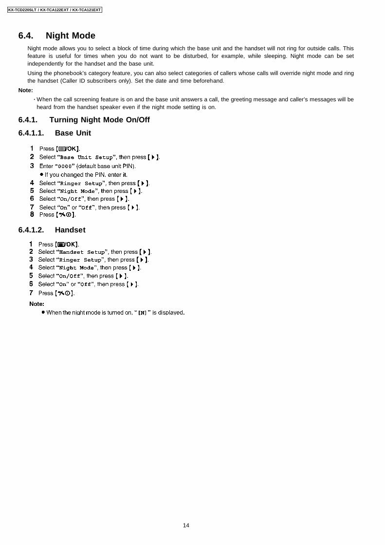
6.4. Night ModeNight mode allows you to select a block of time during which the base unit and the handset will not ring for outside calls. Thisfeature is useful for times when you do not want to be disturbed, for example, while sleeping. Night mode can be setindependently for the handset and the base unit.
Using the phonebook’s category feature, you can also select categories of callers whose calls will override night mode and ringthe handset (Caller ID subscribers only). Set the date and time beforehand.
Note:
· When the call screening feature is on and the base unit answers a call, the greeting message and caller’s messages will beheard from the handset speaker even if the night mode setting is on.
6.4.1. Turning Night Mode On/Off
6.4.1.1. Base Unit
6.4.1.2. Handset
14
KX-TCD220SLT / KX-TCA122EXT / KX-TCA121EXT

6.5. PIN Code
6.5.1. Base Unit
For security, the base unit PIN must be entered when changing certain settings. The default PIN is “ ”.
For Service Hint:
*: If the current 4-digit Base Unit PIN is forgotten, follow the procedures below.
1. If Base Unit and Handset are not linked with, first, follow the steps in Registering a Handset to a Base Unit (P.26).
2. Follow the steps above in Base Unit (P.15) of PIN Code. At step 3, enter , and you will able to enter newBase Unit PIN.
6.5.2. Handset
For security, the handset PIN must be entered when changing certain settings. The default PIN is “ ”.
For Service Hint:
*: If the current 4-digit PIN is forgotten, press and you will be able to enter new Handset PIN.
This password is useful whether Base Unit and Handset are linked with or not.
15
KX-TCD220SLT / KX-TCA122EXT / KX-TCA121EXT

6.6. Reset
6.6.1. Base Unit
Note:
· The following items will be deleted or reset to their default settings:
− − − − Base Unit (P.11) Settings
− − − − All SMS messages
− − − − Caller list
· The following items will be retained:
− − − − Date and time
− − − − Shared phonebook entries
− − − − Repeater mode
− − − − Recordings, including your greeting message, caller messages, voice memos and audible call announcements, andrecorded conversations.
6.6.2. Handset
Note:
· The following items will be deleted or reset to their default settings:
− − − − Handset (P.12) Settings
− − − − Redial list
− − − − Voice enhancer
− − − − Category names
− − − − Category ringtones
· The following items will be retained:
− − − − Handset phonebook entries (category names and ringtones will be reset to their default settings.)
− − − − Date and time
16
KX-TCD220SLT / KX-TCA122EXT / KX-TCA121EXT

6.7. Key LockThe handset can be locked so that no calls or settings can be made. Incoming calls can be answered, but all other functionsare disabled while key lock is on.
Note:
· Calls to emergency numbers cannot be made until key lock is turned off.
· Key lock is turned off when the handset is turned off.
6.8. R Button to Use the Recall Feature[R] is used to access optional telephone services. Contact your service provider for details.
Note:
· If your unit is connected to a PBX (private branch exchange), pressing [R] can allow you to access certain features of yourhost PBX such as transferring an extension call. Consult your PBX dealer for details.
· You can change the recall time.
6.9. Pause Button for PBX/Long Distance Service UsersA pause is sometimes required when making calls using a PBX or long distance service.
Example:
· If you have to dial before dialling outside numbers manually, you will probably pause after dialling until you hear adial tone.
Note:
· Pressing 1 time creates 1 pause. Press repeatedly to create longer pauses.
6.10. Setting Call RestrictionYou can restrict selected handsets from dialling certain numbers. You can assign up to 6 phone numbers to be restricted, andselect which handsets will be restricted.
Storing area codes here will prevent the restricted handsets from dialling any phone number in that area code. If a restrictednumber is dialled, the call will not be connected and the restricted number will flash on the display.
17
KX-TCD220SLT / KX-TCA122EXT / KX-TCA121EXT

6.11. Turning Call BAR On/Off (Call Prohibition)This feature prohibits making outside calls. When call bar is turned on, only intercom calls and calls to emergency numbers canbe made.
Note:
· When call bar is turned on, is displayed.
6.12. Changing the Display Language
6.13. Changing the Recall TimeChange the recall time, if necessary, depending on the requirements of your service provider or PBX.
18
KX-TCD220SLT / KX-TCA122EXT / KX-TCA121EXT

6.14. ARS (Automatic Route Selection)Different telephone carriers charge different rates for call to different areas. If you use different telephone carriers in an effortto save costs, automatic route selection can automatically dial the appropriate carrier code when you make calls to certain areacodes according to the way you program this feature.
Important:
· To use automatic route selection, you must:
− − − − subscribe to the telephone carrier service you use
− − − − store the carrier codes you use
− − − − store the area codes you want to call using a specific carrier code
− − − − assign a carrier code to each stored area code
Contact your telephone carrier(s) for calling rates.
Example:
You have assigned carrier code “9876” to area code “123”. If you dial “123-4567”, the unit dials “9876-123-4567”.
Storing carrier codes for ARS (Turning ARS on)
Storing area codes for ARS
Turning ARS off
19
KX-TCD220SLT / KX-TCA122EXT / KX-TCA121EXT

7 DISPLAY7.1. Display Icons
Various icons appear on the handset display to indicate the current status of the unit.
7.2. Caller ID DisplayImportant:
· This unit is Caller ID compatible. To use Caller ID features (such as displaying caller phone numbers), you must subscribeto Caller ID service. Consult your service provider for details.
Caller ID features
When an outside call is received, the caller’s phone number can be displayed.
· Phone numbers of the last 50 different callers will be logged in the caller list.
· While listening to a message recorded by the answering system, you can call back the caller without having to dial the phonenumber.
· When caller information is received and it matches a phone number stored in the unit’s phonebook:
− − − − The stored name will be displayed and logged in the caller list.
− − − − The handset will use the ringtone assigned to the caller’s category.
− − − − The handset will announce the audible call recording you made.
· If the unit is connected to a PBX system, you may not receive the caller information.
· When the caller dialled from an area which does not provide Caller ID service, “ ” will be displayed.
· When the caller requested not to send caller information, either no information or “ ” will be displayed.
20
KX-TCD220SLT / KX-TCA122EXT / KX-TCA121EXT

8 OPERATIONS
8.1. Turning the Power On/OffPower on
Press for about 1 second.
· The display will change to the standby mode.
Power off
Press for about 2 seconds.
· The display will go blank.
8.2. Setting the Date and TimeImportant:
· Confirm that the AC adaptor is connected.
· Ensure that is not flashing.
Note:
· To correct a digit, press or to move the cursor, then make the correction.
· The date and time may be incorrect after a power failure. In this case, set the date and time again.
8.3. RediallingPreviously dialled phone numbers (each 24 digits max.) can be redialled.
8.3.1. Making a Call Using the Redial List
The last 10 phone numbers dialled are stored in the redial list.
8.3.2. Redialling the Last Number Dialled
21
KX-TCD220SLT / KX-TCA122EXT / KX-TCA121EXT

8.4. PhonebookThe phonebook allows you to make calls without having to dial manually. You can add 200 names and phone numbers to thephonebook, assign each phonebook entry to the desired category, and search for phonebook entries by name or category.
8.4.1. Adding Entries to the Phonebook
Note:
If there is no space to store new entries, “ ” will be displayed. Erase unnecessary entries.
8.4.2. Available Character Entries
22
KX-TCD220SLT / KX-TCA122EXT / KX-TCA121EXT

23
KX-TCD220SLT / KX-TCA122EXT / KX-TCA121EXT

8.4.3. Editing Entries in the Phonebook
Phonebook entries can be edited after you have saved them. You can change the name, phone number, and category.
Changing a name, phone number, category
8.4.4. Erasing Entries from the Phonebook
Erasing an entry
Erasing all entries
8.4.5. Storing a Number from the Caller List into the Phonebook
Cross Reference:
Adding Entries to the Phonebook (P.22)
8.4.6. Storing a Number from the Redial List into the Phonebook
24
KX-TCD220SLT / KX-TCA122EXT / KX-TCA121EXT

8.4.7. One Touch Dial
Assigning an Entry in the Phonebook to a One Touch Dial Key
Making a Call Using a One Touch Dial Key
Erasing a One Touch Dial Assignment
Note:
Only the one touch dial assignment is erased. The corresponding phonebook entry is not erased.
8.4.8. Copying Phonebook Entries to Other Handsets
Phonebook entries can be copied from the handset to the phonebook of a compatible Panasonic handset.
Copying One Entry
Copying All Entries
Note:
· If the other handset (the receiver) is not in standby mode, “ ” is displayed on your handset (the sender).
· If copying failed after copying at least 1 entry, “ ” is displayed on your handset (the sender).
25
KX-TCD220SLT / KX-TCA122EXT / KX-TCA121EXT

8.5. Registering a Handset to a Base UnitTo Register an Additional Handset to a Base Unit (Easy Registration)
The included handset and base unit are preregistered. After purchasing an additional handset, register it to the base unit.Ensure that the additional handset is switched on. If it is not on, press and hold for few seconds to turn the handset on.
Note:
· If an error tone sounds, or if is still flashing, register the handset manually (manual registration).
· If all registered handsets start ringing in step 2, press to stop. Start again from step 1.
· Charge the batteries of your additional handset for about 7 hours before initial use.
· This registration method cannot be used for handsets that have already been registered to a base unit. Register the handsetmanually (manual registration).
To Register a Handset to an Additional Base Unit (Manual Registration)
You can register a handset to a base unit manually using the following method.
8.5.1. Cancelling a Handset
A maximum of 6 handsets can be registered to a base unit. A handset can cancel its own registration (or the registration ofanother handset) that is stored in the base unit. This will allow the base unit to “forget” the handset.
26
KX-TCD220SLT / KX-TCA122EXT / KX-TCA121EXT

8.5.2. Cancelling a Base Unit
A handset can be registered to a maximum of 4 base units. A handset can cancel a base unit that it is registered to. This allowsthe handset to “forget” the base unit.
Note:
To register the handset to another base unit or to the same base unit again, see manual registration.
8.6. Selecting a Base UnitWhen “ ” is selected, the handset will automatically use any available base unit it is registered to. When a specific baseunit is selected, the handset will make and receive calls using that base unit only. If the handset is out of range of that base unit,no calls can be made.
27
KX-TCD220SLT / KX-TCA122EXT / KX-TCA121EXT

9 SMS (Short Message Service)SMS allows you to send and receive text messages between other fixed-line and mobile phones that support compatible SMSnetworks and features.
Messages can be forwarded by your SMS provider to fax machines and e-mail address.
Important:
· To use SMS features, you must:
− − − − subscribe to the Caller ID and/or appropriate service
− − − − confirm SMS is turned on
− − − − confirm the correct message centre numbers are stored
Consult your service provider for details and availability.
Note:
· A total of 47 messages (at 160 characters/message) can be saved. Total number may be more than 47 if length ofmessages are less than 160 characters/message.
· If the unit is connected to a PBX system, you may not be able to use SMS features.
9.1. Writing and Sending a New Message
Note:
· This unit supports SMS messages of up to 612 characters, however, the maximum number of characters you can send orreceive may be limited by your SMS service provider. Consult your SMS service provider for details.
· If your message contains over 160 characters, “ ” is displayed. Your service provider may treat longmessages differently from other messages. Consult your service provider for details.
· “ ” is displayed if you try to send a message to a phone number saved in the phonebook, caller list, orredial list that is over 20 digits long.
· When sending a message, “ ” is displayed momentarily, then “ ” is displayed.
· If your phone is connected to a PBX, store the PBX line access number.
28
KX-TCD220SLT / KX-TCA122EXT / KX-TCA121EXT

9.2. Available Character Entries for SMS
29
KX-TCD220SLT / KX-TCA122EXT / KX-TCA121EXT

9.3. Sending a Saved Message
Cross Reference:
Writing and Sending a New Message (P.28)
9.4. Editing and Sending a Saved Message
Cross Reference:
Writing and Sending a New Message (P.28)
9.5. Erasing Saved Messages
30
KX-TCD220SLT / KX-TCA122EXT / KX-TCA121EXT

9.6. Receiving a MessageWhen an SMS message is received:
- a tone is heard (if the ringer is turned off, this tone is not heard)
- “ ” is displayed
- is displayed
9.7. Reading a Received Message
Note:
· To call the message sender, press or .
· If “ ” is displayed, new SMS messages cannot be received. Erase unnecessary messages.
· If you receive a message from a party saved in the handset phonebook, the stored name is displayed.
· Some SMS service providers attach a 1digit number to the message sender’s phone number, and sender names stored inthe handset phonebook may not be displayed as a result.
9.8. Replying to a Message
Cross Reference:
Writing and Sending a New Message (P.28)
9.9. Erasing Received Messages
31
KX-TCD220SLT / KX-TCA122EXT / KX-TCA121EXT

9.10. Changing SMS Message Centre NumbersSMS message centre telephone numbers must be stored in order to send and receive SMS messages.
The following numbers (used for SMS service provided by Cablecom) are pre programmed in this unit. You can change themif necessary.
- Message Centre 1: 0435375370
· Consult your service provider for more information.
Note:
If your phone is connected to a PBX, you need to add the PBX line access number and a dialling pause to the beginning of theMessage Centre 1 phone number. For Message centre 2, store the Message centre 1 phone number as is, without adding aline access number or dialling pause.
9.11. Turning SMS On/Off
Note:
· If you try to send a message while SMS is turned off, a tone sounds and the message is placed in the receive list with “ ”attached to it.
· If someone tries to send you a message while SMS is turned off, the message will not be received and the message centrenumber will be logged in the caller list.
32
KX-TCD220SLT / KX-TCA122EXT / KX-TCA121EXT

10 Answering System
10.1. Turning the Answering System On/Off
10.2. Greeting Message
10.2.1. Using a prerecorded greeting message
10.2.2. Playing back the greeting message
33
KX-TCD220SLT / KX-TCA122EXT / KX-TCA121EXT

10.3. Listening to MessageMessages are stored and played back chronologically, from oldest message to newest.
10.3.1. Listening to new/all message
10.3.2. Repeating, skipping, stopping, erasing a message during playback
10.3.3. Erasing All Messages
34
KX-TCD220SLT / KX-TCA122EXT / KX-TCA121EXT

10.4. Using Direct Commands
35
KX-TCD220SLT / KX-TCA122EXT / KX-TCA121EXT

10.5. Remote Operation
10.5.1. Turning remote operation on/off
10.5.2. Turning on the answering system remotely
36
KX-TCD220SLT / KX-TCA122EXT / KX-TCA121EXT

11 TROUBLESHOOTINGIf you still have difficulties after following the instructions in this section, disconnect the AC adaptor and turn off the handset,then reconnect the AC adaptor and turn on the handset.
Cross Reference:
(*1) Registering a Handset to a Base Unit (P.26)
(*2) Turning the Power On/Off (P.21)
(*3) Battery Installation (P.6)
(*4) Battery Charge (P.6)
Cross Reference:
(*5) Turning Call BAR On/Off (Call Prohibition) (P.18)
(*6) Setting Call Restriction (P.17)
(*7) Key Lock (P.17)
(*8) Ringer Volume (P.13)
(*9) Night Mode (P.14)
37
KX-TCD220SLT / KX-TCA122EXT / KX-TCA121EXT

Cross Reference:
(*10) Battery Charge (P.6)
(*11) Battery Replacement (P.7)
(*12) Caller ID Display (P.20)
(*13) Cancelling a Base Unit (P.27)
(*14) Cancelling a Handset (P.26)
(*15) PIN Code (P.15)
38
KX-TCD220SLT / KX-TCA122EXT / KX-TCA121EXT

Cross Reference:
(*16) Changing SMS Message Centre Numbers (P.32)
(*17) Erasing Saved Messages (P.30)
(*18) Erasing Received Messages (P.31)
(*19) Turning SMS On/Off (P.32)
Cross Reference:
(*20) Erasing All Messages (P.34)
(*21) Turning remote operation on/off (P.36)
(*22) Turning on the answering system remotely (P.36)
39
KX-TCD220SLT / KX-TCA122EXT / KX-TCA121EXT

12 DISASSEMBLY INSTRUCTIONS
12.1. Base Unit
Shown in Fig.- To Remove Remove1 Cabinet Cover Screws (2.6 × 10)..........(A) × 42 Main P.C. Board Solders
Main P.C. Board3 Small P.C. Board Screw (2.6 x 10).............(B) x 1
Small P.C. Board
40
KX-TCD220SLT / KX-TCA122EXT / KX-TCA121EXT

12.2. Handset
Shown in Fig.- To Remove Remove4 Cabinet Cover Screws (2 × 10)..........(C) × 25 Follow the procedure.6 Main P.C. Board Screw (2 × 10)..............(D) × 1
Screws (2 × 10).............(E) × 2Tapes and SoldersMain P.C. Board
41
KX-TCD220SLT / KX-TCA122EXT / KX-TCA121EXT

12.3. Charger Unit
Shown in Fig.- To Remove Remove7 Cabinet Cover Screws (2.6 × 10)..........(F) × 28 Main P.C. Board Solders
Main P.C. Board
42
KX-TCD220SLT / KX-TCA122EXT / KX-TCA121EXT

13 HOW TO REPLACE THE HANDSET LCD
43
KX-TCD220SLT / KX-TCA122EXT / KX-TCA121EXT
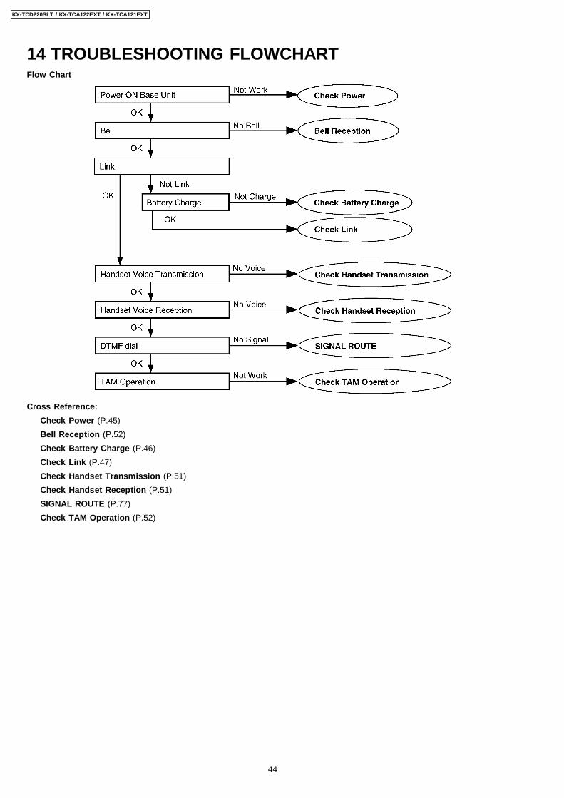
Flow Chart
Cross Reference:
Check Power (P.45)
Bell Reception (P.52)
Check Battery Charge (P.46)
Check Link (P.47)
Check Handset Transmission (P.51)
Check Handset Reception (P.51)
SIGNAL ROUTE (P.77)
Check TAM Operation (P.52)
14 TROUBLESHOOTING FLOWCHART
44
KX-TCD220SLT / KX-TCA122EXT / KX-TCA121EXT

14.1. Check Power
14.1.1. Base Unit
Is the AC Adaptor inserted into AC outlet? (Check AC Adaptor’s specification.)
Cross Reference:
Power Supply Circuit (P.72)
14.1.2. Handset
Cross Reference:
Power Supply Circuit/Reset Circuit (P.75)
45
KX-TCD220SLT / KX-TCA122EXT / KX-TCA121EXT

14.2. Check Battery Charge
14.2.1. Base Unit
Cross Reference:
Charge Circuit (P.75)
14.2.2. Handset
Cross Reference:
Check Power (P.45)
Charge Circuit (P.75)
14.2.3. Charger Unit
Cross Reference:
Charge Circuit (P.75)
46
KX-TCD220SLT / KX-TCA122EXT / KX-TCA121EXT

14.3. Check Link
14.3.1. Base Unit
47
KX-TCD220SLT / KX-TCA122EXT / KX-TCA121EXT
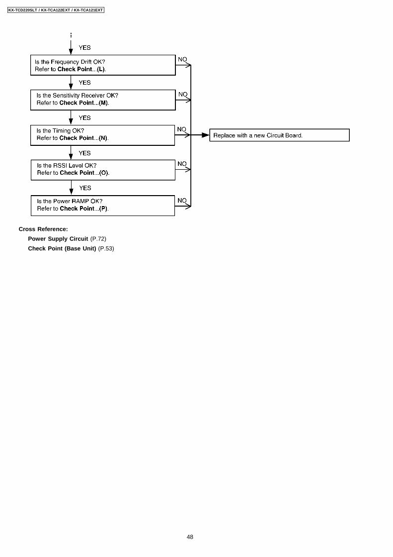
Cross Reference:
Power Supply Circuit (P.72)
Check Point (Base Unit) (P.53)
48
KX-TCD220SLT / KX-TCA122EXT / KX-TCA121EXT

14.3.2. Handset
49
KX-TCD220SLT / KX-TCA122EXT / KX-TCA121EXT

Cross Reference:
Power Supply Circuit/Reset Circuit (P.75)
Check Point (Handset) (P.60)
50
KX-TCD220SLT / KX-TCA122EXT / KX-TCA121EXT

Cross Reference:
SIGNAL ROUTE (P.77)
14.4. Check Handset Transmission
Cross Reference:
SIGNAL ROUTE (P.77)
14.5. Check Handset Reception
Cross Reference:
HOW TO CHECK THE HANDSET SPEAKER OR RECEIVER (P.69).
SIGNAL ROUTE (P.77)
14.6. Check Caller ID
51
KX-TCD220SLT / KX-TCA122EXT / KX-TCA121EXT

14.7. Bell Reception
14.7.1. Base Unit
14.7.2. Handset
Cross Reference:
Telephone Line Interface (P.73)
Check Link (P.47)
HOW TO CHECK THE HANDSET SPEAKER OR RECEIVER (P.69)
14.8. Check TAM Operation
Cross Reference:
Power Supply Circuit (P.72)
52
KX-TCD220SLT / KX-TCA122EXT / KX-TCA121EXT

15 TROUBLESHOOTING BY SYMPTOM (BASE UNIT ANDCHARGER UNIT)
If your unit has below symptoms, follow the instructions in remedy column. Remedies depend on whether you have DECT tester(*1) or not.
Note:
(*1) A general repair is possible even if you don’t have the DECT tester because it is for confirming the levels, such as Acousticlevel in detail.
(*2) Refer to Check Point (Base Unit) (P.53)
15.1. Check Point (Base Unit)Please follow the items below when BBIC or EEPROM or FLASH ROM is replaced.
Note:
After the measuring, sock up the solder of TP.
*: PC Setting (P.65) is required beforehand.
The connections of adjustment equipment are as shown in Adjustment Standard (Base Unit) (P.58).
Items CheckPoint
Procedure Check orReplace Parts
(A) 3.3V SupplyConfirmation
TP14 1. Confirm that the voltage between test point VDD3 and GND is 3.3V ± 0.2V. D1, IC1, C1,C119, C2, R8,
R9, C114, C34,C8, R85
(B) 2.5V SupplyConfirmation
TP22 1. Confirm that the voltage between test point VDD2 and GND is 2.5V ± 0.2V. Q2, C5, C7,C168
(C)* 1.8V SupplyConfirmation
TP15 1. Confirm that the voltage between test point VDD1 and GND is 1.8V ± 0.1V. Q3, C6, C11,C48, C4, C37,C39, C44, C45
(D)* BBIC Confirmation - 1. BBIC Confirmation (Execute the command “getchk”).
2. Confirm the returned checksum value.
Connection of checksum value and program number is shown below.
IC8, X1, C42,C43, R40, C6,C11, C48, C4,
C37, C39, C44,C45, R124,R125, C153
(E)* EEP-ROM Confirmation - 1. EEP-ROM Confirmation (Execute the command “ChkTCD220XXrevYY”).
XX: country code
YY: revision number
2. Confirm the returned checksum value.
Note:“XX”, “YY”, and “checksum” vary depending on the country version. You canfind them in the batch file, PQZZ- mentioned in JIG and PC (P.57).
IC3, C53, R56,R57
(F)* BBIC Clock Adjustment CLK 1. Input Command “rdeeprom 00 01 01”, then you can confirm the current value.
2. Adjust the frequency of CLK executing the command “setfreq xx (where xx isthe value)” so that the reading of the frequency counter is 10.368000MHz ±10Hz.
IC2, IC4, R124,R125, C153,X1, C42, C43
53
KX-TCD220SLT / KX-TCA122EXT / KX-TCA121EXT

Items CheckPoint
Procedure Check orReplace Parts
(G)* Hookswitch Check withDC Characteristics
- 1. Connect CN1 (Telephone Socket) to Tel-simulator which is connected with600 Ω.
2. Set line voltage to 48V and line current to 40mA at off-hook condition ofnormal telephone.
3. Execute the command “hookoff”
4. Confirm that the line current is 40mA ± 5mA.
5. Execute the command “hookon”.
6. Confirm that the line current is less than + 0.8mA.
CN1, L6, L7,Q4, R23, R25,Q5, R26, R28,
IC8, D3
(H)* DTMF Generator Check - 1. Connect CN1 (Telephone Socket) to DTMF tester.
2. Execute the command “hookoff” and “dtmf_hi”.
3. Confirm that the high frequency (1477Hz) is -6.0dBm ~ -10.0dBm.
4. Execute the command “dtmf_lo”.
5. Confirm that the low frequency (852Hz) is -8.5dBm ~ -12.5dBm.
IC8, R39, C41,R49, C46, C47,R42, R43, R44,R45, R46, R47,
R48, C108,C109, C40,C36, Q8, D4
(I)* Transmitted PowerConfirmation
- Remove the Antenna before starting step from 1 to 7. 1. Configure the DECT tester (CMD60) as follows;
<Setting>
· Short A-1 and GND
· Test mode: FP
· Traffic Carrier: 5
· Traffic Slot: 4
· Mode: Loopback
· PMID: 00000
· RF LEVEL = -70dBm.
2. Execute the command “testmode”.
3. Execute the command “sendchar dmv 2 2”.
4. Check that “Signalling Status” has been set to “Locked”, then press “ACCEPTRFPI”.
5. Initiate connection from Dect tester (“set up connect”)
6. Execute the command “ANT1”.
7. Confirm that the NTP value at ANT is 20dBm ~ 25dBm.
IC2, IC8, R124,R125, C153,C140, C141,DA1, C142,
C143, C144, L3,L4, R118, R119,
C135, R115,R116, Q6,
C145, C147,C149, C151,C157, R123,C158, C159,C160, C161,C162, C163,C164, C136,R117, R127,C156, C154,
C155
(J) Modulation Check andAdjustment
- Follow steps 1 to 6 of (I) above.7.Confirm that the B-Field Modulation is -350 ~ -400/+320 ~ +370kHz/divusing data type Fig31.
8.Adjust the B-Field Modulation if required. (Execute the command “readmod”and “wrtmod xx”, where xx is the value.)
IC2, IC8, R124,R125, C153,C140, C141,DA1, C142,
C143, C144, L3,L4, R118, R119,
C135, R115,R116, Q6,
C145, C147,C149, C151,C157, R123,C158, C159,C160, C161,C162, C163,C164, C136,R117, R127,C156, C154,
C155(K) Frequency Offset Check - Follow steps 1 to 6 of (I) above.
7.Confirm that the frequency offset is < ± 45kHz.IC2, IC8, R124,
R125, C153,C140, C141,DA1, C142,
C143, C144, L3,L4, R118, R119,
C135, R115,R116, Q6,
C145, C147,C149, C151,C157, R123,C158, C159,C160, C161,C162, C163,C164, C136,R117, R127,C156, C154,
C155
54
KX-TCD220SLT / KX-TCA122EXT / KX-TCA121EXT
Items CheckPoint
Procedure Check orReplace Parts
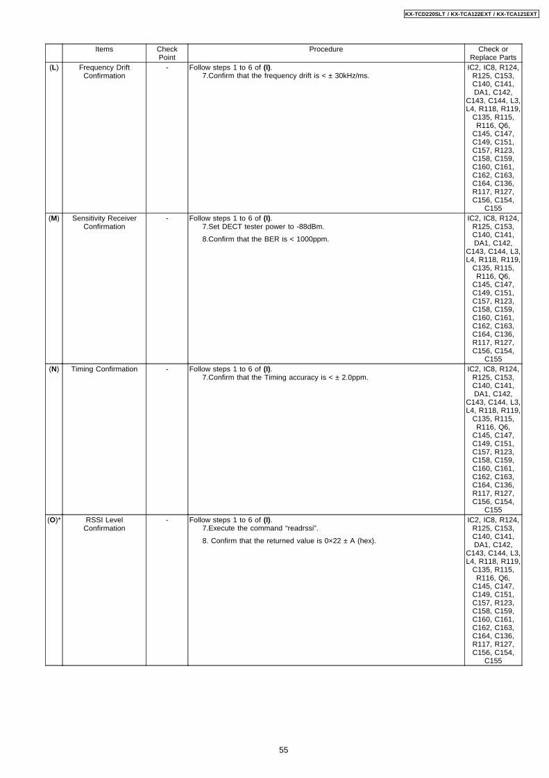
(L) Frequency DriftConfirmation
- Follow steps 1 to 6 of (I).7.Confirm that the frequency drift is < ± 30kHz/ms.
IC2, IC8, R124,R125, C153,C140, C141,DA1, C142,
C143, C144, L3,L4, R118, R119,
C135, R115,R116, Q6,
C145, C147,C149, C151,C157, R123,C158, C159,C160, C161,C162, C163,C164, C136,R117, R127,C156, C154,
C155(M) Sensitivity Receiver
Confirmation- Follow steps 1 to 6 of (I).
7.Set DECT tester power to -88dBm.
8.Confirm that the BER is < 1000ppm.
IC2, IC8, R124,R125, C153,C140, C141,DA1, C142,
C143, C144, L3,L4, R118, R119,
C135, R115,R116, Q6,
C145, C147,C149, C151,C157, R123,C158, C159,C160, C161,C162, C163,C164, C136,R117, R127,C156, C154,
C155(N) Timing Confirmation - Follow steps 1 to 6 of (I).
7.Confirm that the Timing accuracy is < ± 2.0ppm.IC2, IC8, R124,
R125, C153,C140, C141,DA1, C142,
C143, C144, L3,L4, R118, R119,
C135, R115,R116, Q6,
C145, C147,C149, C151,C157, R123,C158, C159,C160, C161,C162, C163,C164, C136,R117, R127,C156, C154,
C155(O)* RSSI Level
Confirmation- Follow steps 1 to 6 of (I).
7.Execute the command “readrssi”.
8. Confirm that the returned value is 0×22 ± A (hex).
IC2, IC8, R124,R125, C153,C140, C141,DA1, C142,
C143, C144, L3,L4, R118, R119,
C135, R115,R116, Q6,
C145, C147,C149, C151,C157, R123,C158, C159,C160, C161,C162, C163,C164, C136,R117, R127,C156, C154,
C155
55
KX-TCD220SLT / KX-TCA122EXT / KX-TCA121EXT

Items CheckPoint
Procedure Check orReplace Parts
(P) Power RAMPConfirmation
- Follow steps 1 to 6 of (I).7.Confirm that Power RAMP is matching.
IC2, IC8, R124,R125, C153,C140, C141,DA1, C142,
C143, C144, L3,L4, R118, R119,
C135, R115,R116, Q6,
C145, C147,C149, C151,C157, R123,C158, C159,C160, C161,C162, C163,C164, C136,R117, R127,C156, C154,
C155(Q)* Audio Check - 1. Link with Handset.
2. Input -45dBm/1kHz to MIC of Handset.
Measure the Level at Line I/F and distortion level.
3. Confirm that the level is -7.5dBm ± 2dBm and that the distortion level is < 5%at TEL Line (600Ω Load).
4. Input -20dBm/1kHz to Line I/F.
Measure the level at Receiver of Handset and distortion level
(*Receive volume set to second position from minimum).
5. Confirm that the level is -20.5dBm ± 2dBm and that the distortion level is <5% at Receiver (Volume Middle, 150Ω Load).
IC8, CN1,SA1,L6, L7, D3, Q4,Q5, R23, R25,
R26, R28
(R) Charging Check - 1. Connect Charge Contact 12Ω/2W resistor between charge+ and charge-.
2. Measure and confirm voltage across the resistor is 2.85V ± 0.2V.
R3, R4, R5, D6,C107, C180,
C181(S) TAM Operation
Confirmation- 1. TAM Confirmation (Execute the command “sendchar_VPI”)
2. Confirm the returned Value (Value is “D597SB”).
IC5, R132,C195, C196,C197, R130,C169, C208,R133, R134,C209, C210
56
KX-TCD220SLT / KX-TCA122EXT / KX-TCA121EXT
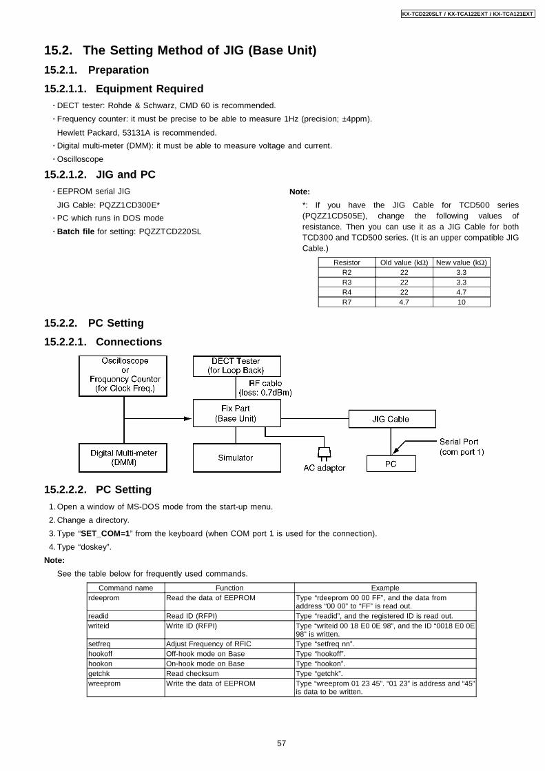
· EEPROM serial JIG
JIG Cable: PQZZ1CD300E*
· PC which runs in DOS mode
· Batch file for setting: PQZZTCD220SL
Note:
*: If you have the JIG Cable for TCD500 series(PQZZ1CD505E), change the following values ofresistance. Then you can use it as a JIG Cable for bothTCD300 and TCD500 series. (It is an upper compatible JIGCable.)
Resistor Old value (kΩ) New value (kΩ)R2 22 3.3R3 22 3.3R4 22 4.7R7 4.7 10
15.2. The Setting Method of JIG (Base Unit)
15.2.1. Preparation
15.2.1.1. Equipment Required · DECT tester: Rohde & Schwarz, CMD 60 is recommended.
· Frequency counter: it must be precise to be able to measure 1Hz (precision; ±4ppm).
Hewlett Packard, 53131A is recommended.
· Digital multi-meter (DMM): it must be able to measure voltage and current.
· Oscilloscope
15.2.1.2. JIG and PC
15.2.2. PC Setting
15.2.2.1. Connections
15.2.2.2. PC Setting
1. Open a window of MS-DOS mode from the start-up menu.
2. Change a directory.
3. Type “SET_COM=1” from the keyboard (when COM port 1 is used for the connection).
4. Type “doskey”.
Note:
See the table below for frequently used commands.
Command name Function Examplerdeeprom Read the data of EEPROM Type “rdeeprom 00 00 FF”, and the data from
address “00 00” to “FF” is read out.readid Read ID (RFPI) Type “readid”, and the registered ID is read out.writeid Write ID (RFPI) Type “writeid 00 18 E0 0E 98”, and the ID “0018 E0 0E
98” is written.setfreq Adjust Frequency of RFIC Type “setfreq nn”.hookoff Off-hook mode on Base Type “hookoff”.hookon On-hook mode on Base Type “hookon”.getchk Read checksum Type “getchk”.wreeprom Write the data of EEPROM Type “wreeprom 01 23 45”. “01 23” is address and “45”
is data to be written.
57
KX-TCD220SLT / KX-TCA122EXT / KX-TCA121EXT

15.3
. A
dju
stm
ent
Sta
nd
ard
(Bas
eU
nit
)W
hen
conn
ectin
gth
eS
imul
ato
rE
quip
men
tfo
rch
ecki
ng,
plea
sere
fer
tobe
low
.
BU
Z
CLKVD
D2
VD
D3
TP
16
TP
15
A_1
A_2
AN
T
VD
D1
J101
TP
19
TP
20
RE
D
BLAC
K
J104
J103
J102
Cop
per
plat
e
LIN
E_D
C
L2T
L1T
CN
1
L2R
L1R
DC
P
DC
M
Pb
F
PC
Dig
ital
Vol
t Met
er
(A)
(B)
(C)
(D)
(E)
TX
J102
RX
J103
GN
DJ1
04G
ND
VD
D2
CH
AR
GE
-
CH
AR
GE
+T
P16
TP
15
Dig
ital
Vol
t Met
er12
Ω2W
(R)
GN
D
CLK
Freq
uenc
yC
ount
er(F
)
AF
OS
CA
F V
olt
Met
er
Dum
my
Han
dset
SP
MIC
OS
C
150Ω
6.3V
47u
F+ -
AN
TG
ND
DE
CT
Tes
ter
CM
D60
(I)
(J)
(K)
(L)
(M)
(N)
(O)
(P)
DC
PG
ND
DC
PO
WE
R6V
BE
LLS
imul
ator
Loop
Sim
ulat
orA
F V
olt
Met
er
AF
OS
CCal
l-ID
Sim
ulat
or
DT
MF
Test
er
L1T
L1R
OS
C
600Ω
(H)
(G)
(Q)
GN
D
GN
D
BU
Z
LIN
E_D
CD
igita
lV
olt M
eter
AF
Vol
t Met
er
VD
D1
VD
D3
No
te:
(A)
-(R
)is
refe
rred
toC
hec
kP
oin
t(B
ase
Un
it)
(P.5
3)
KX-TCD220SLT / KX-TCA122EXT / KX-TCA121EXT
58

15.4. Check Point (Charger Unit)Items Check
PointProcedure Check or
Replace Parts(A) Charging Check - 1. Connect Charge Contact 12Ω/2W resistor between charge+ and charge-.
2. Measure and confirm voltage across the resistor is 2.85V ± 0.2V.
D11, R11, R12
Note:
After the measuring, sock up the solder of TP.
The connection of adjustment equipment is as shown in Adjustment Standard (Charger Unit) (P.59).
15.5. Adjustment Standard (Charger Unit)When connecting the Simulator Equipment for checking, please refer to below.
15.5.1. Flow Solder Side View
TP3
TP2
TP1
A
D11
WHITE
BLUE
PbF
TP4
PQUP11305Z
DC POWER6V
GND (TP2)TP3
GND (TP2)TP1
(A)Digital
Volt Meter
12Ω/2W
R12
R11
R1
R2
Note:
(A) is referred to Check Point (Charger Unit) (P.59)
59
KX-TCD220SLT / KX-TCA122EXT / KX-TCA121EXT

16 TROUBLESHOOTING BY SYMPTOM (HANDSET)If your unit has below symptoms, follow the instructions in remedy column. Remedies depend on whether you have DECT tester(*1) or not.
Note:
(*1) A general repair is possible even if you don’t have the DECT tester because it is for confirming the levels, such as Acousticlevel in detail.
(*2) Refer to Check Point (Handset) (P.60)
16.1. Check Point (Handset)Please follow the items below when BBIC or EEPROM is replaced.
Note:
After the measuring, sock up the solder of TP.
*: PC Setting (P.65) is required beforehand.
The connections of adjustment equipment are as shown in Adjustment Standard (Handset) (P.66).
Items CheckPoint
Procedure Check orReplace Parts
(A)* 1.8V Supply Adjustment VDD1 1. Confirm that the voltage between test point VDD1 and GND is 1.8V ± 0.02V.
2. Execute the command “bandgap”, then check the current value.
3. Adjust the 1.8V voltage of VDD1 executing command “bandgap XX“(XX is thevalue).
IC1, Q2, C40
(B) DC/DC SupplyConfirmation
VDD3 1. Confirm that the voltage between test point VDD3 and GND is 3.3V ± 0.3V(Backlight is ON).
IC1, F1, C1,C3, C57, R1,Q1, D1, L1,57
(C) 2.5V SupplyConfirmation
VDD2 1. Confirm that the voltage between test point VDD2 and GND is 2.5V ± 0.1V. IC1, Q3, C4,C5
(D)* BBIC Confirmation - 1. BBIC Confirmation (Execute the command “getchk”).
2. Confirm the returned checksum value.
Connection of checksum value and program number is shown below.
IC1, X1,C7,R19
(E)* EEP-ROM Confirmation - 1. EEP-ROM Confirmation (Execute the command “ChkTCA121XXrevYY”).
XX: country code
YY: revision number
2. Confirm the returned checksum value.
Note:“XX”, “YY”, and “checksum” vary depending on the country version. You canfind them in the batch file, PQZZ- mentioned in JIG and PC (P.57).
IC3, IC1, R39,R40, R91,R90, R96,Q10, Q11,
C113
60
KX-TCD220SLT / KX-TCA122EXT / KX-TCA121EXT
Items CheckPoint
Procedure Check orReplace Parts
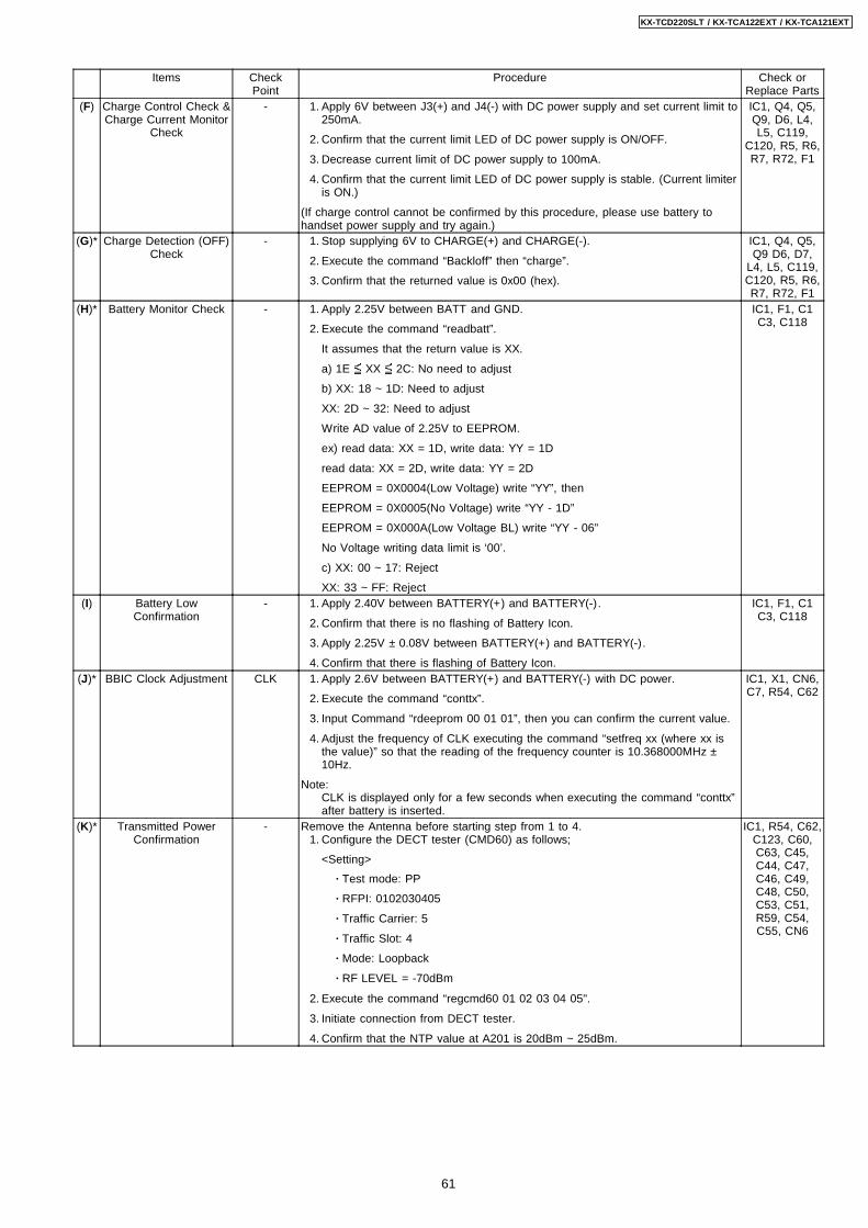
(F) Charge Control Check &Charge Current Monitor
Check
- 1. Apply 6V between J3(+) and J4(-) with DC power supply and set current limit to250mA.
2. Confirm that the current limit LED of DC power supply is ON/OFF.
3. Decrease current limit of DC power supply to 100mA.
4. Confirm that the current limit LED of DC power supply is stable. (Current limiteris ON.)
(If charge control cannot be confirmed by this procedure, please use battery tohandset power supply and try again.)
IC1, Q4, Q5,Q9, D6, L4,L5, C119,
C120, R5, R6,R7, R72, F1
(G)* Charge Detection (OFF)Check
- 1. Stop supplying 6V to CHARGE(+) and CHARGE(-).
2. Execute the command “Backloff” then “charge”.
3. Confirm that the returned value is 0x00 (hex).
IC1, Q4, Q5,Q9 D6, D7,
L4, L5, C119,C120, R5, R6,R7, R72, F1
(H)* Battery Monitor Check - 1. Apply 2.25V between BATT and GND.
2. Execute the command “readbatt”.
It assumes that the return value is XX.
a) 1E XX 2C: No need to adjust
b) XX: 18 ~ 1D: Need to adjust
XX: 2D ~ 32: Need to adjust
Write AD value of 2.25V to EEPROM.
ex) read data: XX = 1D, write data: YY = 1D
read data: XX = 2D, write data: YY = 2D
EEPROM = 0X0004(Low Voltage) write “YY”, then
EEPROM = 0X0005(No Voltage) write “YY - 1D”
EEPROM = 0X000A(Low Voltage BL) write “YY - 06”
No Voltage writing data limit is ‘00’.
c) XX: 00 ~ 17: Reject
XX: 33 ~ FF: Reject
IC1, F1, C1C3, C118
(I) Battery LowConfirmation
- 1. Apply 2.40V between BATTERY(+) and BATTERY(-).
2. Confirm that there is no flashing of Battery Icon.
3. Apply 2.25V ± 0.08V between BATTERY(+) and BATTERY(-).
4. Confirm that there is flashing of Battery Icon.
IC1, F1, C1C3, C118
(J)* BBIC Clock Adjustment CLK 1. Apply 2.6V between BATTERY(+) and BATTERY(-) with DC power.
2. Execute the command “conttx”.
3. Input Command “rdeeprom 00 01 01”, then you can confirm the current value.
4. Adjust the frequency of CLK executing the command “setfreq xx (where xx isthe value)” so that the reading of the frequency counter is 10.368000MHz ±10Hz.
Note:CLK is displayed only for a few seconds when executing the command “conttx”after battery is inserted.
IC1, X1, CN6,C7, R54, C62
(K)* Transmitted PowerConfirmation
- Remove the Antenna before starting step from 1 to 4. 1. Configure the DECT tester (CMD60) as follows;
<Setting>
· Test mode: PP
· RFPI: 0102030405
· Traffic Carrier: 5
· Traffic Slot: 4
· Mode: Loopback
· RF LEVEL = -70dBm
2. Execute the command “regcmd60 01 02 03 04 05".
3. Initiate connection from DECT tester.
4. Confirm that the NTP value at A201 is 20dBm ~ 25dBm.
IC1, R54, C62,C123, C60,C63, C45,C44, C47,C46, C49,C48, C50,C53, C51,R59, C54,C55, CN6
61
KX-TCD220SLT / KX-TCA122EXT / KX-TCA121EXT

Items CheckPoint
Procedure Check orReplace Parts
(L)* Modulation Check andAdjustment
- Follow steps 1 to 3 of (K) above.4.Confirm that the B-Field Modulation is -350 ~ -400/+320 ~ +370kHz/div usingdata type Fig 31.
5.Adjust the B-Field Modulation if required. (Execute the command “Readmod”and “wrtmod xx”, where xx is the value.)
IC1, R54, C62,C123, C60,C63, C45,C44, C47,C46, C49,C48, C50,C53, C51,R59, C54,C55, CN6
(M) Frequency OffsetConfirmation
- Follow steps 1 to 3 of (K) above.4.Confirm that the frequency Offset is < ± 45kHz.
IC1, R54, C62,C123, C60,C63, C45,C44, C47,C46, C49,C48, C50,C53, C51,R59, C54,C55, CN6
(N) Frequency DriftConfirmation
- Follow steps 1 to 3 of (K).4.Confirm that the frequency Drift is < ± 30kHz/ms.
IC1, R54, C62,C123, C60,C63, C45,C44, C47,C46, C49,C48, C50,C53, C51,R59, C54,C55, CN6
(O) Sensitivity ReceiverConfirmation
- Follow steps 1 to 3 of (K).4.Set DECT tester power to -88dBm.
5.Confirm that the BER is < 1000ppm.
IC1, R54, C62,C123, C60,C63, C45,C44, C47,C46, C49,C48, C50,C53, C51,R59, C54,C55, CN6
(P) Timing Confirmation - Follow steps 1 to 3 of (K).4.Confirm that the Timing accuracy is < ± 2.0ppm.
IC1, R54, C62,C123, C60,C63, C45,C44, C47,C46, C49,C48, C50,C53, C51,R59, C54,C55, CN6
(Q)* RSSI LevelConfirmation
- Follow steps 1 to 3 of (K).4.Set DECT tester power to -81dBm.
5.Execute the command “readrssi“.
6.Confirm that the returned value is 0×1C ± 8 (hex).
7.Set DECT tester power to -63dBm.
8.Execute the command “readrssi“.
9.Confirm that the returned value is 0×25 ± 8 (hex).
IC1, R54, C62,C123, C60,C63, C45,C44, C47,C46, C49,C48, C50,C53, C51,R59, C54,C55, CN6
(R) Power RAMPConfirmation
- Follow steps 1 to 3 of (K).4.Confirm that Power RAMP is matching.
IC1, R54, C62,C123, C60,C63, C45,C44, C47,C46, C49,C48, C50,C53, C51,R59, C54,C55, CN6
(S) Audio Check andConfirmation
- 1. Link to BASE which is connected to Line Simulator.
2. Set line voltage to 48V and line current to 40mA.
3. Input -45dBm/1KHz to MIC and measure Line output level.
4. Confirm that the level is -7.5dBm ± 2dBm and that the distortion level is < 5%at TEL Line (600Ω Load).
5. Input -20dBm/1KHz to Line I/F and measure Receiving level at REV1 andREV2.
6. Confirm that the level is -20.5dBm ± 2dBm and that the distortion level is < 5%at Receiver. (vol = 2)
IC1, C37, C68,C91, R25,R26, C20,C12, C87,C109, R85,C103, C10,C17, R86,R29, R37,
R38, D4, D5,C69, C70, C95
62
KX-TCD220SLT / KX-TCA122EXT / KX-TCA121EXT

Items CheckPoint
Procedure Check orReplace Parts
(T) SP phone Audio Checkand Confirmation
- 1. Link to Base which is connected to Line Simulator.
2. Set line voltage to 48V and line current to 40mA.
3. Set the handset off-hook using SP-Phone key.
4. Input -25dBm/1KHz to Line I/F and measure Receiving level at SP1 and SP2.
5. Confirm that the level is -15.5dBm ± 2dBm and that the distortion level is < 5%.(vol = 3)
IC1, C37, C68,C91, R25,R26, C20,C12, C87,C109, R85,C103, C10,C17, R86,R29, R37,
R38, L6, L7,C79, C78
63
KX-TCD220SLT / KX-TCA122EXT / KX-TCA121EXT

16.2. Troubleshooting for SpeakerphoneWhen the customer’s telephone line corresponds to the following conditions, and the transmission signal of SP-Phone isinterrupted, performing the next set up to a cordless handset will improve it to some extent.
Conditions
1. When customer’s line has less line loss.
ex.) The customer is using optical fiber, ISDN terminal adaptor, or PBX.
In this case, receiving signal is strong and it may affect transmission signal.
2. When the other party is talking from noisy place.
ex.) The other party is using cellular phone. The background noise is very loud.
In this case, the noise from the other party (i.e. surrounding noise) may affect transmission signal.
Setting Method
· Change the address of EEPROM (0×0144) from 0×00 to 0×01.
64
KX-TCD220SLT / KX-TCA122EXT / KX-TCA121EXT

· EEPROM serial JIG
JIG Cable: PQZZ1CD300E*
· PC which runs in DOS mode.
· Batch file for PC setting: PQZZTCD220SL
Note:
*: If you have the JIG Cable for TCD500 series(PQZZ1CD505E), change the following values ofresistance. Then you can use it as a JIG Cable for bothTCD300 and TCD500 series. (It is an upper compatible JIGCable.)
Resistor Old value (kΩ) New value (kΩ)R2 22 3.3R3 22 3.3R4 22 4.7R7 4.7 10
16.3. The Setting Method of JIG (Handset)
16.3.1. Preparation
16.3.1.1. Equipment Required · DECT tester: Rohde & Schwarz, CMD 60 is recommended.
· Frequency counter: it must be precise to be able to measure 1Hz (precision; ±4ppm).
Hewlett Packard, 53131A is recommended.
· DC power: it must be able to output at least 1A current under 2.4V for Handset.
· Digital multi-meter (DMM): it must be able to measure voltage and current.
· Oscilloscope
16.3.1.2. JIG and PC
16.3.2. PC Setting
16.3.2.1. Connections
16.3.2.2. PC Setting
1. Open a window of MS-DOS mode from the start-up menu.
2. Change a directory.
3. Type “SET_COM=1” from the keyboard (when COM port 1 is used for the connection).
4. Type “doskey”.
Note:
See the table below for frequently used commands.
Command name Function Examplerdeeprom Read the data of EEPROM Type “rdeeprom 00 00 FF”, and the data from
address “00 00” to “FF” is read out.readid Read ID (RFPI) Type “readid”, and the registered ID is read out.writeid Write ID (RFPI) Type “writeid 00 18 E0 0E 98”, and the ID “0018 E0 0E
98” is written.setfreq Adjust Frequency of RFIC Type “setfreq nn”.getchk Read checksum Type “getchk”.wreeprom Write the data of EEPROM Type “wreeprom 01 23 45”. “01 23” is address and “45”
is data to be written.
65
KX-TCD220SLT / KX-TCA122EXT / KX-TCA121EXT

16.4
. A
dju
stm
ent
Sta
nd
ard
(Han
dse
t)W
hen
conn
ectin
gth
eS
imul
ato
rE
quip
men
tfo
rch
ecki
ng,
plea
sere
fer
tobe
low
.
C66
A201
ANT
R59
C54C55
C45R54
R55
C46C47
R62
Q5
Q9
J3
TP
22
CHG CHG
TP
23
J2
UTX
URX
J4
C58
C97
C102
C68C37C91
R85
C6
C19
R19R82
C82
SP
_TE
ST
1
REV_TEST1
REV_TEST2
SP
_TE
ST
2
C60
C59
C123
C64
C61C65
C44 C62
CLKC63
D1
R93
C119
R6
R47
R46
R86R25 R29
C10
C101
C107
C108
C111
C112
F1
J1
C3
R1
R83
R43
C98
L9
L7
L6
C95
C78
C79
VD
D3
D7
D6
D9 Q
8
D10
C40
R5
L5L4
R74
C80
R36
C76
C16
C92
R80
C13
C83C69 C70
C81
C86
C15
R35R67 R66
C14
R34C75
C38
C77
R61
R71
R40
R39
R64
D5
D8
D4
R60
JTA
G
R63
VD
D1
VD
D2
PO
WE
R
R91
C93
C41
C4
C94
C22
C72
R15
R57
R96
C116
C117
C12
2
C11
3
C24
R68
C10
0 C20
C7
R21
R20
BA
TG
ND
C57
C1
C53
CN
6
C51
C50
C48
C49
C67
A
1726
101
C84
R75
PbF
IC1
IC3
IC2
X1C
21R90
C18C96
R92
R72
C99
C23
R87
R7
C11
4R
94
C120
C115
C71
R89
R88
C39
R26
C90
C10
3
R38
R37
C17
C10
9C
87C
12
L1
R12
R81
C118
C104
C5
C8
Q4
Q11
Q2
Q3
Q10
Q1
Q7
PQ
UP
1127
8Z
1
1
1
8
8
4
4
5
5
20
8061
6041
2140
Cur
rent
Pro
be
DC
6V
Osc
illos
cope
AF
G
ener
ator
AF
V
olt M
eter
DE
CT
test
er
CM
D60
/CT
S60
Osc
illos
cope
A B 1
DC
PO
WE
R
BA
TT
LOW
2.00
-2.2
5
Pow
er k
ey
150Ω
56Ω
1
F
56Ω
8Ω
AF
Vol
tM
eter OS
C
AF
OS
C600Ω
Loop
Dum
my
Bas
eU
nit
RE
V-
RE
V+
SP
+P
ower
TP
20
2.7V
TP
21
SP
-
AN
TG
ND
6.3V
47u
F
Zen
er
Bat
tery
+B
atte
ry-
DC
PO
WE
R2.
30-2
.60V
PC
UR
XU
TX
GN
D
GN
D
BA
T
Dig
ital
Vol
t Met
er
GN
DG
ND
VD
D1
VD
D2
VD
D3
Fre
quen
cyC
ount
er
CLK
100Ω
22pF
Sim
ulat
or
(S)
(T)
(K)
~ (
R)
(F)
(S)
(T)
(D)
(E)
(G)
(H)
(A)
(B)
(C)
(J)
(I)
No
te:
(A)
-(T
)is
refe
rred
toC
hec
kP
oin
t(H
and
set)
(P.6
0)
KX-TCD220SLT / KX-TCA122EXT / KX-TCA121EXT
66

17 THINGS TO DO AFTER REPLACING ICCautions:
Since this page is common to each country, it may not apply to some models in your country. The contents below are theminimum adjustments required for operation.
17.1. Base UnitIC Necessary Adjustment
BBIC Programs for Voice processing, interface for RF andEEPROM
1. Default batch file: Execute the command “default”.
2. Country version batch file: Execute the command“TCD220XXrevYY”. (*1)
3. Clock adjustment: Refer to Check Point (F). (*2)EEPROM Adjustment parameter data
(country version batch file, default batch file, etc.) 1. Change the address “0000” of EEPROM to “AA”.
2. Default batch file: Execute the command “default”.
3. Country version batch file: Execute the command“TCD220XXrevYY”. (*1)
4. Clock adjustment: Refer to Check Point (F). (*2)FLASH 1 Voice prompt data
(vary depending on country version)No need to adjust
Note:
(*1) XX: country code, YY: revision number
“XX” and “YY” vary depending on the country version. You can find them in the batch file, PQZZ- mentioned in JIG and PC(P.57).
(*2) Refer to Check Point (Base Unit) (P.53)
17.2. HandsetIC Necessary Adjustment
BBIC Programs for Voice processing, interface for RF andEEPROM
1. Default batch file: Execute the command “default”.
2. Default batch file (remaining); Execute the command“TCA121 DEFrevYY”. (*3)
(Except for KX-TCA121/122 FX and KX-TCA121/122 RU).
3. Country version batch file: Execute the command“TCA121XXrevYY”. (*3)
4. Clock adjustment: Refer to Check Point (J). (*4)
5. 1.8 V setting and battery low detection: Refer to CheckPoint (A), (H) and (I). (*4)
EEPROM Adjustment parameter data(country version batch file, default batch file, etc.)
1. Change the address “0015” of EEPROM to “55”.
2. Default batch file: Execute the command “default”.
3. Default batch file (remaining): Execute the command“TCA121DEFrevYY”. (*3)
(Except for KX-TCA121/122 FX and KX-TCA121/122 RU).
4. Country version batch file: Execute the command“TCA121XXrevYY”. (*3)
5. Clock adjustment: Refer to Check Point (J). (*4)
6. 1.8 V setting and battery low detection: Refer to CheckPoint (A), (H) and (I). (*4)
Note:
(*3) XX: country code, YY: revision number
“XX” and “YY” vary depending on the country version. You can find them in the batch file, PQZZ- mentioned in JIG and PC(P.57).
(*4) Refer to Check Point (Handset) (P.60)
67
KX-TCD220SLT / KX-TCA122EXT / KX-TCA121EXT
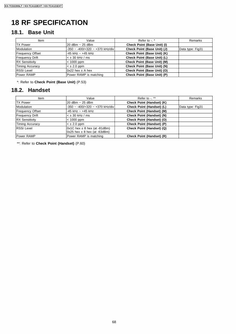
18 RF SPECIFICATION18.1. Base Unit
Item Value Refer to -. * RemarksTX Power 20 dBm ~ 25 dBm Check Point (Base Unit) (I)Modulation -350 ~ -400/+320 ~ +370 kHz/div Check Point (Base Unit) (J) Data type: Fig31Frequency Offset -45 kHz ~ +45 kHz Check Point (Base Unit) (K)Frequency Drift < ± 30 kHz / ms Check Point (Base Unit) (L)RX Sensitivity < 1000 ppm Check Point (Base Unit) (M)Timing Accuracy < ± 2.0 ppm Check Point (Base Unit) (N)RSSI Level 0x22 hex ± A hex Check Point (Base Unit) (O)Power RAMP Power RAMP is matching Check Point (Base Unit) (P)
*: Refer to Check Point (Base Unit) (P.53)
18.2. HandsetItem Value Refer to -. ** Remarks
TX Power 20 dBm ~ 25 dBm Check Point (Handset) (K)Modulation -350 ~ -400/+320 ~ +370 kHz/div Check Point (Handset) (L) Data type: Fig31Frequency Offset -45 kHz ~ +45 kHz Check Point (Handset) (M)Frequency Drift < ± 30 kHz / ms Check Point (Handset) (N)RX Sensitivity < 1000 ppm Check Point (Handset) (O)Timing Accuracy < ± 2.0 ppm Check Point (Handset) (P)RSSI Level 0x1C hex ± 8 hex (at -81dBm)
0x25 hex ± 8 hex (at -63dBm)Check Point (Handset) (Q)
Power RAMP Power RAMP is matching Check Point (Handset) (R)
**: Refer to Check Point (Handset) (P.60)
68
KX-TCD220SLT / KX-TCA122EXT / KX-TCA121EXT

19 HOW TO CHECK THE HANDSET SPEAKER ORRECEIVER
1. Prepare the digital voltmeter, and set the selector knob to ohm meter.
2. Put the probes at the speaker terminals as shown below.
20 FREQUENCY TABLE (MHz)BASE UNIT HANDSET
Channel No Transmit Frequency Receive Frequency Transmit Frequency Receive Frequency1 1897.344 1897.344 1897.344 1897.3442 1895.616 1895.616 1895.616 1895.6163 1893.888 1893.888 1893.888 1893.8884 1892.160 1892.160 1892.160 1892.1605 1890.432 1890.432 1890.432 1890.4326 1888.704 1888.704 1888.704 1888.7047 1886.976 1886.976 1886.976 1886.9768 1885.248 1885.248 1885.248 1885.2489 1883.520 1883.520 1883.520 1883.52010 1881.792 1881.792 1881.792 1881.792
Note:
Channel No. 10: In the Test Mode on Base Unit and Handset.
69
KX-TCD220SLT / KX-TCA122EXT / KX-TCA121EXT
21 B
LO
CK
DIA
GR
AM
(BA
SE
UN
IT)
Ana
log
Fro
ntE
nd
To
TE
L_LI
NE
A B
CN
1
Brid
geR
ect D
3 D
3H
ook
Sw
itch
Q4,
Q5
Aud
io
Bel
l/Cal
ler
IDIn
terf
ace
Ana
log
Sw
itch
CP
U
59 54 61 52 60 56 55B
ELL
HO
OK
Off-
Hoo
k Li
ne V
olta
ge64
AD
CO
D/A
A/D
AD
PC
MC
odec
Filt
er
DS
P
Spe
ech
Dec
odin
g
Spe
ech
Enc
odin
g
BM
C
Bur
st D
ecod
ing
Bur
st E
ncod
ing R
FIn
terf
ace
18 19
RX
DA
TX
DA
15 2120 22
RS
SI
SY
CL
SY
DA
SY
EN
AN
T1
AN
T2
RF
Mod
ule
4 10
231
8
2114 13 12
12 13
XT
AL
X1
10.3
68M
Hz
EE
PR
OM
SC
L
SD
A
6 5T
o A
C A
dapt
or
CN
1
Lim
itR
esis
tor
CH
AR
GE
CO
NT
AC
T
VU
NR
EG
3.3V
Reg
.IC
1
2.5V
Reg
.Q
2
1.8V
Reg
.Q
33.3V
2.5V
1.8V
BB
ICIC
3
FLA
SH
ME
MO
RY
(TA
M)
RE
SE
T
CS
23 36
SC
K
SI
38 39
SO
40IC
5
IC8
IC2
KX
-TC
D22
0 B
LOC
K D
IAG
RA
M (
BA
SE
UN
IT)
KX-TCD220SLT / KX-TCA122EXT / KX-TCA121EXT
70

22 CIRCUIT OPERATION (BASE UNIT)22.1. Outline
Base Unit consists of the following ICs as shown in BLOCK DIAGRAM (BASE UNIT) (P.70).
· DECT BBIC (Base Band IC): IC8
− − − − Handling all the audio, signal and data processing needed in a DECT base unit
− − − − Controlling the DECT specific physical layer and radio section (Burst Module Controller section)
− − − − ADPCM codec filter for speech encoding and speech decoding (DSP section)
− − − − Echo-cancellation and Echo-suppression (DSP section)
− − − − Any tones (tone, sidetone, ringing tone, etc.) generation (DSP section)
− − − − DTMF receiver (DSP section)
− − − − Clock Generation for RF Module
− − − − ADC, DAC, timer, and power control circuitry
− − − − All interfaces (ex: RF module, EEPROM, LED, Analog Front End, etc.)
· RF Module: IC2
− − − − PLL Oscillator
− − − − Detector
− − − − Compress/Expander
− − − − First/Second Mixer
− − − − Amplifier for transmission and reception
· EEPROM: IC3
− − − − Temporary operating parameters (for RF, etc.)
· Additionally,
− − − − Power Supply Circuit (+3.3V, +2.5V, +1.8V output)
− − − − Crystal Circuit (10.368MHz)
− − − − Charge Circuit
− − − − Telephone Line Interface Circuit
· FLASH MEMORY: IC5
− − − − Voice Prompt (TAM) D/L Area
− − − − ICM/OGM/MEMO recording area
71
KX-TCD220SLT / KX-TCA122EXT / KX-TCA121EXT

22.2. Power Supply CircuitThe power is supplied to the DECT BBIC, RF Module, EEPROM and Charge Contact from AC Adaptor (+6V) as shown inFig.101. The power supply is as follows;
· DECT BBIC (IC8):
CN1 (+6V) → D1 → IC1 → Q2 → IC8
· RF Module (IC2):
CN1 (+6V) → D1 → IC1 → Q2 → IC2 (PLL)
CN1 (+6V) → D1 → IC1 → IC2 (Power AMP)
· EEPROM (IC3):
CN1 (+6V) → D1 → IC1 → Q2 → IC3
· FLASH MEMORY (IC5):
CN1 (+6V) → D1 → IC1 → IC5
· Charge Contact (TP15):
CN1 (+6V) → D1 → R3, R5 → TP15
<Fig.101>
72
KX-TCD220SLT / KX-TCA122EXT / KX-TCA121EXT

22.3. Telephone Line Interface<Function>
· Bell signal detection
· Clip signal detection
· ON/OFF hook circuit
· Audio circuits
· DTMF tone signal circuits
Bell & Clip (: Calling Line Identification Presentation: Caller ID) signal detection:
In the standby mode, Q4 is open to cut the DC loop current and decrease the ring load.
When ring voltage appears at the TP2 (A) and TP3 (B) leads (when the telephone rings), the AC ring voltage is transferred asfollows;
· A → C13 → R17 → R24 → IC8 Pin 60 (CID INp)
· B → C12 → R16 → R32 → IC8 Pin 52 (CID INn)
ON/OFF hook circuit:
In the standby mode, Q4 is open, and connected as to cut the DC loop current and to cut the voice signal. The unit isconsequently in an off-hook condition.
When IC2 detects a ring signal or press the TALK Key onto the handset, Q5 turns on and then Q4 turns on, thus providing anoff-hook condition (active DC current flow through the circuit) and the following signal flow is for the loop current.
· A → D3 → Q4 → Q8 → R45 → R46 → D3 → B [OFF HOOK]
22.4. Transmitter/ReceiverBase Unit and Handset mainly consist of RF Module and DECT BBIC.
Base Unit and Handset transmit/receive voice signal and data signal through the antenna on carrier frequency.
Signal Path:
*Refer to SIGNAL ROUTE (P.77).
22.4.1. Transmitter Block
The voice signal input from the TEL LINE interface goes to RF Module (IC2) through DECT BBIC (IC8) as shown in BLOCKDIAGRAM (BASE UNIT) (P.70)
The voice signal passes through the analog part of IC8 where it is amplified and converted to a digital audio stream signal. Theburst switch controller processes this stream performing encryption and scrambling, adding the various other fields to producethe GAP (Generic Access Profile) standard DECT frame, assigning to a time slot and channel etc.
In IC2, the carrier frequency is changing, and frequency modulated RF signal is generated and amplified, and radiated fromantenna. Handset detects the voice signal or data signal in the circuit same as the following explanation of Receiver Block.
22.4.2. Receiver Block
The signal of 19.2 MHz band (18.81792 MHz ~ 18.97344 MHz) which is input from antenna is input to IC2 as shown in BLOCKDIAGRAM (BASE UNIT) (P.70).
In IC2, the signal of 19.2 MHz band is downconverted to 864 kHz signal and demodulated, and goes to IC8 as GAP (GenericAccess Profile) standard DECT frames. It passes through the decoding section burst switch controller where it separates outthe frame information and performs de-encryption and de-scrambling as required. It then goes to the DSP section where it isturned back into analog audio. This is amplified by the analog front end, and goes to the TEL LINE Interface.
73
KX-TCD220SLT / KX-TCA122EXT / KX-TCA121EXT

23 BLOCK DIAGRAM (HANDSET)
SPEAKER
RECEIVER
MIC
CHARGECIRCUITQ4,Q5,Q9R7
CHARGECONTACTS
CHARGE(+)
CHARGE(-)
CHARGE
CHARGE DETECT
EEPROMSCL
SDA
SWITCHEDSUPPLY Q1Q1
BATTERYTERMINAL
D7
VBAT1
DC/DC-SWITCH
J1
J2
2.5VQ3
1.8VQ2
4.0V 2.5V
1.8V
LCD
RS
RESETCS
SI
SCL
CPU
AnalogFrontEnd
D/A
A/D
30
3266
6772
62
52
45
44
58
56
59
60
6
9
10
77
ADPCMCodecFilter
DSP
SpeechDecodingSpeech
Encoding
BMC
BurstDecoding
BurstEncoding
RFInterface
RFModule
CN6
23
22
RXDA
TXDA
19
2625
24
RSSISYDASYENSYCL
16
17
XTALX1
10.368MHz
BATTERY
61
ON SWITCH
KEYPAD
ROWS
COLUMNS
1,12,40,76
27,28,34,35,36,74
BBICIC1
IC3
11
LCD-BACK LIGHT
KEY-BACK LIGHT
SP-PHONE LIGHT
7
75
46
KX-TCA122/121 BLOCK DIAGRAM (HANDSET)
74
KX-TCD220SLT / KX-TCA122EXT / KX-TCA121EXT
24 CIRCUIT OPERATION (HANDSET)24.1. Outline
Handset consists of the following ICs as shown in BLOCK DIAGRAM (HANDSET) (P.74).
· DECT BBIC (Base Band IC): IC1
− − − − All data signals (forming/analyzing ACK or CMD signal)
− − − − All interfaces (ex: Key, Detector Circuit, Charge, DC/DC Converter, EEPROM, LCD)
· RF Module: CN6
− − − − PLL Oscillator
− − − − Detector
− − − − Compress/Expander
− − − − Amplifier for transmission and reception
· EEPROM: IC3
− − − − Temporary operating parameters (for RF, etc.)
24.2. Power Supply Circuit/Reset CircuitCircuit Operation:
When power on the Handset, the voltage is as follows;
BATTERY(2.2 V ~ 2.6 V: J1) → L1, D1 → Q2 (1.8 V), Q3 (2.5 V), Q1 (3.3 V)
The Reset signal generates IC1 (53 pin) and 1.8 V.
24.3. Charge CircuitCircuit Operation:
When charging the handset on the Base Unit, the charge current is as follows;
DC+(5.5V ~ 6V) → D1 → R4, R5 → CHARGE+(Base) → CHARGE+(Handset) → L4 → Q4 → D7→ F1 → BATTERY+...Battery... BATTERY- → R43 → GND → L5 → CHARGE-(Handset)→ CHARGE-(Base) → GND → DC-(GND)
In this way, the BBIC on Handset detects the fact that the battery is charged.
The charge current is controlled by switching Q5 of Handset.
Refer to Fig.101 in Power Supply Circuit (P.72).
24.4. Battery Low/Power Down DetectorCircuit Operation:
“Battery Low” and “Power Down” are detected by BBIC which check the voltage from battery.
The detected voltage is as follows;
· Battery Low
Battery voltage: V(Batt) 2.25V ± 50mV
The BBIC detects this level and " " starts flashing.
· Power Down
Battery voltage: V(Batt) 2.0V ± 50mV
The BBIC detects this level and power down.
Refer to Check Point (Handset) (P.60).
24.5. SpeakerphoneThe hands-free loudspeaker at SP+ and SP- is used to generate the ring alarm.
Refer to Troubleshooting for Speakerphone (P.64).
75
KX-TCD220SLT / KX-TCA122EXT / KX-TCA121EXT

25 CIRCUIT OPERATION (CHARGER UNIT)25.1. Power Supply CircuitThe power supply is as shown.
76
KX-TCD220SLT / KX-TCA122EXT / KX-TCA121EXT

26 SIGNAL ROUTE
77
KX-TCD220SLT / KX-TCA122EXT / KX-TCA121EXT

78
KX-TCD220SLT / KX-TCA122EXT / KX-TCA121EXT

27 CPU DATA (BASE UNIT)27.1. IC8 (BBIC)
Pin No Description I/O Connection at Normal mode at Reset mode1 INT1n/P1_1 D,O RLY O I-PU2 VDDIO - - - -3 VDD - - - -4 VSS - - - -5 SDA1/P2_5 D,I/O SDA I/O I6 SCL1/P2_4 D,O SCL O I7 INT5n/P1_5 D,O NC O-L I-PU8 INT2n/P1[2] D,O P1[2]9 AVD - - - -
10 AVS - - - -11 CAP A,I CAP I I12 Xtal1 A,I Xtal1 I -13 VSSRF - - - -14 RFCLKp A,I NC O Hi-Z15 RSSI/RFCLKm A,I RSSI I Hi-Z16 VDDRF - - - -17 RFCLKd D,O RFCLKd O O-L18 TDO A,O TDO O -19 RDI D,I RDI I I20 SK D,I/O SK - O-L21 PD1/SIO D,I/O SIO - I-PD22 LE D,I/O LE O O-H23 P3[1]/PD1 D,I/O P3[1] O I-PD24 P3[2]/PD2 D,I/O P3[2] O I-PD25 P3[3]/PD3 D,I/O P3[3] O I-PD26 P3[4]/PD4 D,I/O P3[4] O I-PD27 TDOD/P3[5]/PD5 D,I/O P3[5] O I-PD28 P3[6]/PD6 D,O NC O I-PD29 VSS - - - -30 VDDIO - - - -31 VDD - - - -32 PCM_FSC/INT0n/P1[0] D,I/O INT0n O I-PU33 P0[0]/UTX D,I/O UTX O I-PU34 P0[1]/URX D,I/O URX O I-PU35 P0[2]/JTIO D,I/O JTIO O I-PU36 P0[3]/SDA2 D,I/O P0[3] O I-PU37 P0[4]/SCL2 D,I/O P0[4] O I-PU38 P0[5]/SPICLK/PCM_CLK D,I/O SPICLK O I-PU39 P0[6]/SPIDO/PCM_DOUT D,I/O SPIDO O I-PU40 P0[7]/SPIDI/PCM_DIN D,I/O SPIDI O I-PU41 VSS - - - -42 VDD - - - -43 P2[3]/ADC1 I ADC1 I I44 P1[7]/CHARGE/INT7 I CHARGE I I-PD45 RSTn I RSTn I I-PU46 VBAT1 A,I VBAT1 I I47 LDO1_CTRL D,O LDO1_CTRL O O-H48 LDO2_CTRL D,O LDO2_CTRL O O-H49 LDO1_Sense D,I LDO1_Sense I O-L50 AVS2 - - -51 AVD2 - - - -52 CIDINn A,I CIDINn I I53 LSRn/REF A,O REF O O54 LSRp/REF A,O LSRp O O55 RINGING A,I RINGING I I56 MICn/CIDOUT A,I CIDOUT O O57 VREFm - - - -58 AGND A,O AGND O O59 MICp A,I MICp I I60 CIDINp A,I CIDINp I I61 P1[4]/INT4n D,I/O P1[4] I I62 P1[3]/INT3n D,I/O P1[3] I I
79
KX-TCD220SLT / KX-TCA122EXT / KX-TCA121EXT
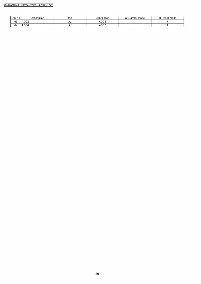
Pin No Description I/O Connection at Normal mode at Reset mode63 ADC2 A,I ADC2 I I64 ADC0 A,I ADC0 I I
80
KX-TCD220SLT / KX-TCA122EXT / KX-TCA121EXT

28 CPU DATA (HANDSET)28.1. IC1 (BBIC)
Pin No Description I/O Connection at Normal mode at Reset mode1 INTln/P1[1] D,I ROW1 I I-PU2 VDDIO - - - -3 VDD - - - -4 VSS - - - -5 LED1/PWM0/P2[0] D,O PWM0 O-L I-PU6 LED2/PWM1/P2[1] D,O LCD_CSB O-H I-PU7 LED3 A,I LED_BKL I I8 LED_BIAS/P3[6]/PD A.O LED_BIAS O I-PD9 SDA1/P2[5] D,I/O LCD_SI I/O I10 SCL1/P2[4] D,O LCD_SCL O I11 INT5n/VDDE/P1[5] D,O LCD_RS O-L I-PU12 INT2n/P1[2] D,I ROW2 I I-PU13 AVD - - - -14 AVS - - - -15 CAP A,I CAP I I16 Xta11 A,I XtaI1 I -17 VSSRF - - - -18 RFCLKp A,O NC O Hi-Z19 RSSI/RFCLKm A,I RSSI I Hi-Z20 VDDRF - - - -21 RFCLKd D,O RFCLKd O O-L22 TDD A,O TDO O -23 RDI D,I RDI I I24 SK D,I/O SK - O-L25 PD1/SIO D,I/O SIO - I-PD26 LE D,I/O LE O-L O-H27 P3[1]/PD1 D,I/O COL1 O-L I-PD28 P3[2]/PD2 D,I/O COL2 O-L I-PD29 VSSPA - - - -30 PAOUTm D,O PAOUTm O O31 VDDPA - - - -32 PAOUTp D,O PAOUTp O O33 VSSPA - - - -34 P3[3]/PD3 D,I/O COL3 O-L I-PD35 P3[4]/PD4 D,I/O COL4 O-L I-PD36 TDOD/P3[5]/PD5 D,I/O COL5 O-L I-PD37 VSS - - - -38 VDDIO - - - -39 VDD - - - -40 PCM_FSC/INT0n/P1[0] D,I ROW0 I I-PU41 P0[0]/UTX D,I/O UTX O I-PU42 P0[1]/URX D,I/O URX O I-PU43 P0[2]/JTIO D,I/O JTIO O I-PU44 P0[3]/SDA2 D,I/O P0[3] O I-PU45 P0[4]/SCL2 D,I/O P0[4] O I-PU46 P0[5]/SPICLK/PCM D,I/O SP_LED O I-PU47 P0[6]/SPIDO/PCM_D D,O CD_AMP O I-PU48 P0[7]/SPIDI/PCM_D D,I/O RESET O I-PU49 VSS - - - -50 VDD - - - -51 P2[3]/ADC1 O EEP_WP O O52 P1[7]/CHARGE/INT7 I CHARGE I I-PD53 RSTn I RSTn I I-PU54 DC_stab O DC_stab O O55 DC_1 I DC_I I I56 DC_CTRL O DC_CTRL O O-PD57 DC_Sence I DC_Sence I I58 VBAT1 A,I VBAT1 I I59 LDO1_CTRL D,O LDO1_CTRL O O-H60 LDO2_CTRL D,O LDO2_CTRL O O-H61 P1[6]/PON/INT6 I power_det I I-PD62 P2[6]/stop_charge A,O stop_charge O O-O
81
KX-TCD220SLT / KX-TCA122EXT / KX-TCA121EXT

Pin No Description I/O Connection at Normal mode at Reset mode63 LDO1_Sense D,I LDO1_Sense I O-L64 AVS2 - - - -65 AVD2 - - - -66 LSRn/REF A,O REF O O67 LSRp/REF A,O LSRp O O68 MICn A,I RINGING I I69 VREFm - - - -70 VBUF O VBUF O O71 AGND A,O AGND O O72 MICp A,I MICp I I73 VREFp A,I CIDINp I I74 P3[0] D,I/O COL0 O-L I-PD75 P1[4]/INT4n D,O Key_LED O O-L76 P1[3]/INT3n D,I ROW3 I I77 P2[2]/CLK100 D,O LCD_RESET O I-PD78 AVS_sence I AVS_sence I I79 ADC2 A,I ADC2 I I80 ADC0 A,I NC I I
82
KX-TCD220SLT / KX-TCA122EXT / KX-TCA121EXT

29 ENGINEERING MODE29.1. Base Unit
83
KX-TCD220SLT / KX-TCA122EXT / KX-TCA121EXT

Note:
*: When you enter the address, please refer to the table below.
Desired Number Input Keys Desired Number Input Keys0 0 A [R] + 01 1 B [R] + 1. . C [R] + 2. . D [R] + 3. . E [R] + 49 9 F [R] + 5
ex.)
Items (*2) Address Default Data New Data RemarksC-ID (FSK) sensitivity 04 3D 00 01 (6dB up) 02 (12dB up) When hex changes from “00” to “01” or “02”, gain
increases by 6dB or 12dB.C-ID (DTMF) sensitivity 04 4B 50 60 (6dB up) 70 (12dB up) When hex changes from “50” to “60” or “70”, gain
increases by 6dB or 12dB.SMS (FSK) receivingsensitivity
04 3D 00 01 (6dB up) 02 (12dB up) When hex changes from “00” to “01” or “02”, gainincreases by 6dB or 12dB.
SMS (FSK) sendinglevel
04 56/04 57 00/0B 00/16 (6dBup)
00/2C (12dBup)
When hex changes from “00 0B” to “00 16” or “002C”, gain increases by 6dB or 12dB.
Frequency 00 01 75 - - Use these items in a READ-ONLY mode to confirmthe contents. Careless rewriting may cause seriousdamage to the computer system.
ID 00 10~00 14 Given value - -
Bell length 01 F6 32 (5sec) (*1) 1E (3sec) 14 (2sec) This is time until bell stops ringing. (Unit: 100ms)
(*1) 32 (hex) = 50 (dec) → 50 × 100msec = 5000msec (5sec)
(*2)
84
KX-TCD220SLT / KX-TCA122EXT / KX-TCA121EXT

Items DescriptionC-ID (FSK) sensitivity FSKGain_shiftgainC-ID (DTMF) sensitivity Foutgains:HPFilter FoutgainsSMS (FSK) receiving sensitivity FSKGain_shiftgainSMS (FSK) sending level wFskAttn:Signal Output Attenuation (DSP parameter)Frequency Setting value of FREQ_TRIM_REGID IDBell length Time until it stops bell.
85
KX-TCD220SLT / KX-TCA122EXT / KX-TCA121EXT

29.2. Handset
86
KX-TCD220SLT / KX-TCA122EXT / KX-TCA121EXT

(*1) When adding “01” (hex) to default value, sending levelincreases by 0.25dB.
ex.)
Item Default Data New Data3A 3E 36
Sending level -7.5dBm -6.5dBm -8.5dBm
(*2) When reducing “01” (hex) from default value, receivinglevel increases by 0.25dB.
ex.)
Item Default Data New Data14 18 10
Receiving level -20.5dBm -21.5dBm -19.5dBm
Note:
*: When you enter the address, please refer to the table in Note: of ENGINEERING MODE (P.83).
ex.)
Items (*4) Address Default Data New Data Possible AdjustedValue MAX (hex)
Possible AdjustedValue MIN (hex)
Remarks
Sending level 00 06 Adjusted value Given value 6F 00 (*1)Receiving level 00 07 Adjusted value Given value 00 3F (*2)Battery Low 00 04 25 - - -
(*3)Frequency 00 01 75 - - -ID 00 10~00 14 Given value - - -
(*3) Use these items in a READ-ONLY mode to confirm the contents. Careless rewriting may cause serious damage to thecomputer system.
(*4)
Items DescriptionSending level Analog Front End MIC Setting for Handset ModeReceiving level Analog Front End LSR Setting for Handset ModeBattery Low ADC value for battery low detectionFrequency Setting value of FREQ_TRIM_REGID International Portable Part Equipment Identities
87
KX-TCD220SLT / KX-TCA122EXT / KX-TCA121EXT

30 HOW TO REPLACE THE FLAT PACKAGE ICEven if you do not have the special tools (for example, a spot heater) to remove the Flat IC, with some solder (large amount),a soldering iron and a cutter knife, you can easily remove the ICs that have more than 100 pins.
30.1. PREPARATION · PbF (: Pb free) Solder
· Soldering Iron
Tip Temperature of 700°F ± 20°F (370°C ± 10°C)
Note: We recommend a 30 to 40 Watt soldering iron. An expert may be able to use a 60 to 80 Watt iron where someone withless experience could overheat and damage the PCB foil.
· Flux
Recommended Flux: Specific Gravity → 0.82.
Type → RMA (lower residue, non-cleaning type)
Note: See ABOUT LEAD FREE SOLDER (PbF: Pb free) (P.4)
30.2. FLAT PACKAGE IC REMOVAL PROCEDURE 1. Put plenty of solder on the IC pins so that the pins can be completely covered.
Note:
If the IC pins are not soldered enough, you may give pressure to the P.C. board when cutting the pins with a cutter.
2. Make a few cuts into the joint (between the IC and its pins) first and then cut off the pins thoroughly.
3. While the solder melts, remove it together with the IC pins.
When you attach a new IC to the board, remove all solder left on the land with some tools like a soldering wire. If some solder isleft at the joint on the board, the new IC will not be attached properly.
88
KX-TCD220SLT / KX-TCA122EXT / KX-TCA121EXT

30.3. FLAT PACKAGE IC INSTALLATION PROCEDURE 1. Temporarily fix the FLAT PACKAGE IC, soldering the two marked pins.
*Check the accuracy of the IC setting with the corresponding solderingfoil.
2. Apply flux to all pins of the FLAT PACKAGE IC.
3. Solder the pins, sliding the soldering iron in the direction of the arrow.
30.4. BRIDGE MODIFICATION PROCEDURE 1. Lightly resolder the bridged portion.
2. Remove the remaining solder along the pins using a soldering iron as shown in the figure below.
89
KX-TCD220SLT / KX-TCA122EXT / KX-TCA121EXT
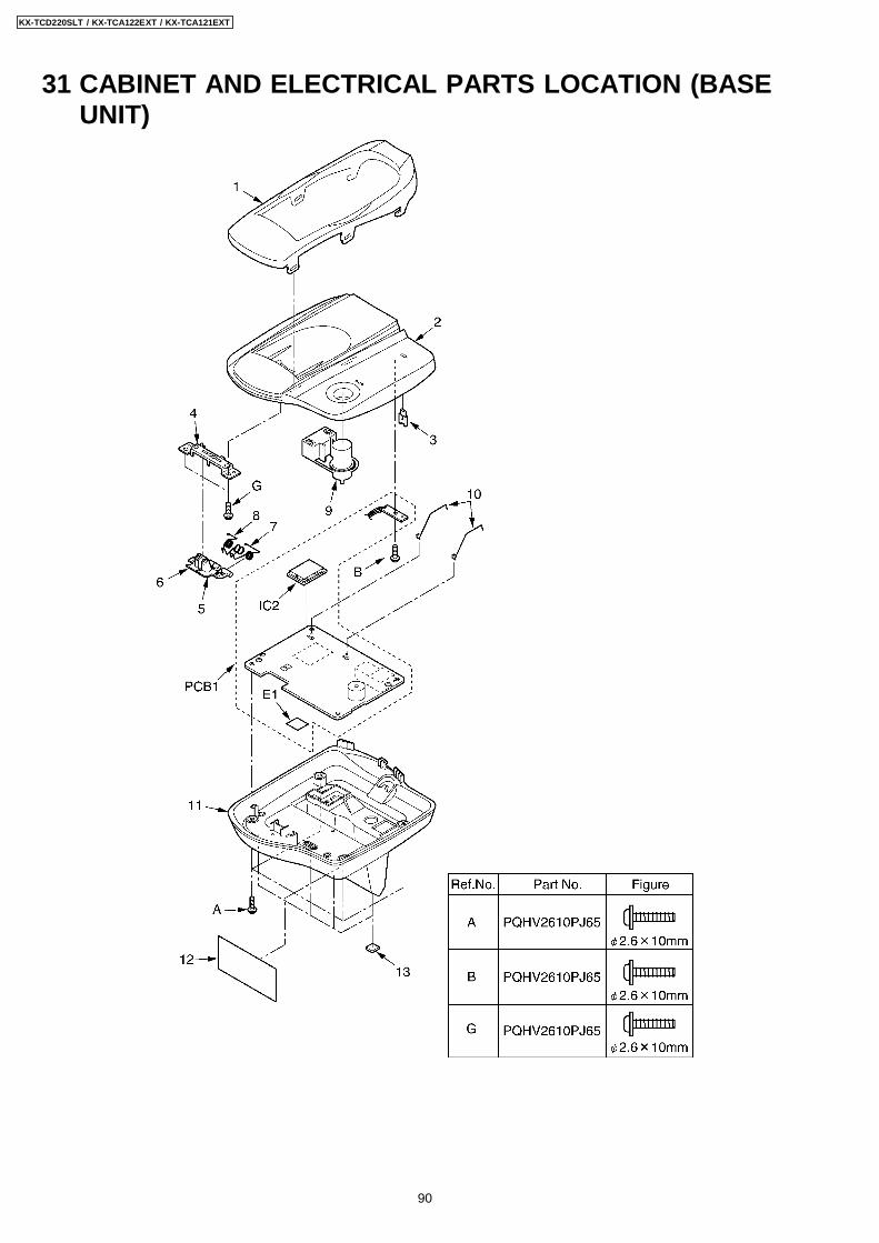
31 CABINET AND ELECTRICAL PARTS LOCATION (BASEUNIT)
90
KX-TCD220SLT / KX-TCA122EXT / KX-TCA121EXT

32 CABINET AND ELECTRICAL PARTS LOCATION(HANDSET)
Note:
(*1) The rechargeable Ni-MH battery P03P (HHR-4EPT) is available through sales route of Panasonic.
(*2) Attach the spacer (No. 122) to the exact location described above.
(*3) This cable is fixed by welding. Refer to HOW TO REPLACE THE HANDSET LCD (P.43).
91
KX-TCD220SLT / KX-TCA122EXT / KX-TCA121EXT

33 CABINET AND ELECTRICAL PARTS LOCATION(CHARGER UNIT)
92
KX-TCD220SLT / KX-TCA122EXT / KX-TCA121EXT

34 ACCESSORIES AND PACKING MATERIALS
34.1. KX-TCD220SLT
93
KX-TCD220SLT / KX-TCA122EXT / KX-TCA121EXT

34.2. KX-TCA121EXT
94
KX-TCD220SLT / KX-TCA122EXT / KX-TCA121EXT

35 TERMINAL GUIDE OF THE ICs, TRANSISTORS ANDDIODES
35.1. Base Unit
35.2. Handset
35.3. Charger Unit
95
KX-TCD220SLT / KX-TCA122EXT / KX-TCA121EXT

1. RTL (Retention Time Limited)
Note:
The marking (RTL) indicates that the Retention Time islimited for this item.
After the discontinuation of this assembly in production,the item will continue to be available for a specific periodof time. The retention period of availability is dependanton the type of assembly, and in accordance with thelaws governing part and product retention. After the endof this period, the assembly will no longer be available.
2. Important safety notice
Components identified by the mark indicates specialcharacteristics important for safety. When replacing any ofthese components, only use specified manufacture’s parts.
3. The S mark means the part is one of some identical parts.For that reason, it may be different from the installed part.
4. ISO code (Example: ABS-94HB) of the remarks columnshows quality of the material and a flame resisting gradeabout plastics.
5. RESISTORS & CAPACITORS
Unless otherwise specified;
All resistors are in ohms (Ω) K=1000Ω, M=1000kΩ
All capacitors are in MICRO FARADS (µF)P=µµF
*Type & Wattage of Resistor
36.1. Base Unit
36.1.1. Cabinet and Electrical PartsRef.No.
Part No. Part Name & Description Remarks
1 PQGG10265Z3 GRILLE PC-HB
2 PQKM10657Z3 CABINET BODY PS-HB
3 PQHR11091Z OPTIC CONDUCTIVE PARTS, LEDLENS
ABS-HB
4 PQHR11057Z CASE, CHARGE TERMINAL PS-HB
5 PQKE10384Z1 HOLDER, CHARGE TERMINAL (R) POM-HB
6 PQKE10385Z1 HOLDER, CHARGE TERMINAL (L) POM-HB
7 PQJT10218Y CHARGE TERMINAL (R)
8 PQJT10219Y CHARGE TERMINAL (L)
Ref.No.
Part No. Part Name & Description Remarks
9 PQBC10415Z1 PUSH BUTTON ABS-HB
10 PQSA10154Z ANTENNA
11 PQKF10631Z3 CABINET COVER PS-HB
12 PQGT17758X NAME PLATE
13 PQHA10023Z RUBBER PARTS, FOOT CUSHION
36.1.2. Main P.C.Board Parts
Note:
(*1) When replacing IC3 or IC8, data need to be written tothem with PQZZTCD220SL. Refer to Base Unit (P.67) ofTHINGS TO DO AFTER REPLACING IC .
Ref.No.
Part No. Part Name & Description Remarks
PCB1 PQWPCD220SLH MAIN P.C.BOARD ASS´Y (RTL)
(ICs)
IC1 C0CBAYF00016 IC
IC3 PQWICD300EH IC (EEPROM) (*1)
IC5 PQWI2D220SLH IC (FLASH MEMORY)
IC7 C0JBAS000248 IC
IC8 C1CB00002005 IC (BBIC) (*1)
(TRANSISTORS)
Q2 B1ADGE000004 TRANSISTOR(SI) S
Q3 B1ADGE000004 TRANSISTOR(SI) S
Q4 2SA1776P TRANSISTOR(SI) S
Q5 PQVTBF822T7 TRANSISTOR(SI)
Q6 B1ADGE000004 TRANSISTOR(SI) S
Q8 2SD1994A TRANSISTOR(SI)
Q14 PSVTDTC143X TRANSISTOR(SI) S
Q15 B1ABGE000006 TRANSISTOR(SI) S
Q16 B1ABCF000103 TRANSISTOR(SI)
(DIODES)
D1 B0JAME000095 DIODE(SI)
D3 B0EDER000009 DIODE(SI)
D4 MA1Z300 DIODE(SI) S
D6 MA8220 DIODE(SI) S
D13 MA111 DIODE(SI) S
D16 MA111 DIODE(SI) S
D17 PQVDBR1111C DIODE(SI) S
DA1 B0DDCM000001 DIODE(SI)
(COILS)
L3 PQLQR2M33NKT COIL S
L6 PQLQXF330K COIL S
L7 PQLQXF330K COIL S
L8 MQLRER10JFA COIL
L9 PQLQR2KA20T COIL S
L10 MQLRER10JFA COIL
C133 PQLQR2M8N2KT COIL S
C139 PQLQR2M5N6K COIL S
(JACK)
CN1 PQJJ2H003Z JACK S
(RESISTORS)
R3 ERJ1WYJ220 22
R5 ERJ1WYJ220 22
R8 ERJ2RKF1200 120
R9 ERJ2RKF2000 200
R16 ERJ3GEYJ105 1M
R17 ERJ3GEYJ105 1M
R22 D0GA104JA015 100K
R23 ERJ3GEYJ104 100K
R24 ERJ3GEYJ101 100
R25 PQ4R10XJ272 2.7K S
R26 ERJ3GEYJ103 10K
R27 D0GA104JA015 100K
R28 ERJ3GEYJ222 2.2K
R32 ERJ3GEYJ101 100
R37 PQ4R10XJ180 18 S
R38 D0GA104JA015 100K
R39 ERJ3GEYJ180 18
36 REPLACEMENT PARTS LIST
96
KX-TCD220SLT / KX-TCA122EXT / KX-TCA121EXT

Ref.No.
Part No. Part Name & Description Remarks
R40 ERJ3GEYJ335 3.3M
R42 ERJ3GEYJ273 27K
R43 D0GA822JA015 8.2K
R44 ERJ3GEYJ182 1.8K
R45 ERJ12YJ120 12
R46 ERJ12YJ270 27
R47 ERJ3GEYJ104 100K
R48 ERJ3GEYJ473 47K
R49 ERJ3GEYJ560 56
R52 D0GA391JA015 390
R54 D0GA182JA015 1.8K
R55 D0GA102JA015 1K
R56 D0GA222JA015 2.2K
R57 ERJ3GEYJ222 2.2K
R64 ERJ3GEYJ102 1K
R69 ERJ3GEYJ104 100K
R70 ERJ3GEYJ104 100K
R71 ERJ3GEYJ104 100K
R72 ERJ3GEYJ474 470K
R84 ERJ3GEYJ101 100
R85 D0GA332JA015 3.3K
R86 D0GA102JA015 1K
R87 D0GA103JA015 10K
R88 D0GA103JA015 10K
R105 D0GA103JA015 10K
R106 ERJ3GEYJ184 180K
R107 ERJ3GEYJ184 180K
R115 ERJ3GEYJ222 2.2K
R116 PQ4R10XJ471 470 S
R117 D0GA102JA015 1K
R118 ERJ3GEYJ271 270
R119 ERJ3GEYJ271 270
R123 D0GAR00Z0001 0
R124 D0GAR00Z0001 0
R125 D0GAR00Z0001 0
R127 D0GA101JA015 100
R129 ERJ3GEYJ681 680
R130 ERJ3GEYJ103 10K
R132 ERJ3GEYJ103 10K
R133 ERJ3GEYJ331 330
R134 ERJ3GEYJ102 1K
R135 D0GA103JA015 10K
R136 D0GA103JA015 10K
R137 D0GA103JA015 10K
R138 ERJ8GEYJ270 27
R139 D0GA471JA015 470
R140 D0GA102JA015 1K
R141 D0GA153JA015 15K
R142 D0GA122JA015 1.2K
R143 ERJ3GEYJ181 180
C167 PQ4R10XJ180 18 S
J13 ERJ12Y0R00 0
J14 ERJ12Y0R00 0
L4 ERJ3GEY0R00 0
(CAPACITORS)
C1 ECUV1H100DCV 10P
C2 ECEA1CK101 100 S
C3 ECEA0JU331 330 S
C4 ECEA1CKS100 10
C5 ECEA1CKS100 10
C6 ECUV1H100DCV 10P
C7 ECUV1A105KBV 1
C8 ECUV1H100DCV 10P
C11 ECUV1A105KBV 1
C12 F1B2H152A048 0.0015
C13 F1B2H152A048 0.0015
C14 ECKD2H681KB 680P S
C15 ECKD2H681KB 680P S
C17 F1G1H221A571 220P
C21 ECJ0EC1H100D 10P
C22 F1G1H221A571 220P
C24 ECUV1C104KBV 0.1
C25 ECJ0EC1H100D 10P
Ref.No.
Part No. Part Name & Description Remarks
C26 ECJ0EC1H220J 22P
C27 ECJ0EC1H100D 10P
C28 ECUV1A224KBV 0.22
C29 ECUV1H100DCV 10P
C30 ECUV1C104KBV 0.1
C32 ECUE1A223KBQ 0.022
C34 F1G1A1040006 0.1
C36 ECUV1H100DCV 10P
C37 F1G1A1040006 0.1
C38 F1G1A1040006 0.1
C39 ECUV1A105KBV 1
C40 PQCUV1A225KB 2.2
C41 ECUV1C563KBV 0.056
C42 ECUV1H060DCV 6P
C43 ECJ0EC1H270J 27P
C44 F1G1A1040006 0.1
C45 F1G1A1040006 0.1
C46 PQCUV1A105KB 1
C47 ECUV1C563KBV 0.056
C48 F1G1A1040006 0.1
C49 ECEA1HKS100 10 S
C50 PQCUV1H104ZF 0.1 S
C53 F1G1A1040006 0.1
C65 F1G1A1040006 0.1
C75 ECUV1H100DCV 10P
C76 ECUV1H103KBV 0.01
C101 ECUV1H102KBV 0.001
C102 ECUV1H102KBV 0.001
C107 ECUV1H102KBV 0.001
C108 PQCUV1A225KB 2.2
C109 ECUV1A105KBV 1
C114 ECJ0EC1H020C 2P
C119 PQCUV1A225KB 2.2
C122 ECUV1H101JCV 100P
C123 ECJ0EC1H101J 100P
C130 ECJ0EC1H100D 10P
C135 PQCUV1C105KB 1
C136 ECJ0EB1H102K 0.001
C140 ECUV1H100DCV 10P
C141 ECUV1H030CCV 3P
C142 ECUV1H100DCV 10P
C143 ECUV1H100DCV 10P
C144 ECUV1H100DCV 10P
C145 ECUV1H100DCV 10P
C146 ECUV1C104KBV 0.1
C149 ECUV1H100DCV 10P
C151 ECUV1A475KB 4.7
C153 ECJ0EC1H220J 22P
C154 ECJ0EC1H100D 10P
C155 ECJ0EC1H020C 2P
C156 ECJ0EC1H100D 10P
C157 ECJ0EC1H070D 7P
C158 ECJ0EC1H100D 10P
C159 ECJ0EC1H020C 2P
C160 ECJ0EC1H100D 10P
C161 ECJ0EC1H020C 2P
C162 ECJ0EC1H100D 10P
C163 ECJ0EC1H100D 10P
C164 F1G1H151A541 150P
C169 ECUV1C104KBV 0.1
C171 ECUV1H102KBV 0.001
C172 ECJ0EC1H101J 100P
C173 ECJ0EC1H100D 10P
C174 F1G1A1040006 0.1
C180 ECUV1H100DCV 10P
C181 ECUV1H100DCV 10P
C182 ECUV1H100DCV 10P
C183 ECUV1H070CCV 7P
C184 ECUV1H100DCV 10P
C191 ECUV1H100DCV 10P
C192 ECUV1H100DCV 10P
C193 ECJ0EC1H100D 10P
C194 ECUV1H100DCV 10P
97
KX-TCD220SLT / KX-TCA122EXT / KX-TCA121EXT

Ref.No.
Part No. Part Name & Description Remarks
C195 ECUV1H100DCV 10P
C196 ECUV1H100DCV 10P
C197 ECUV1H100DCV 10P
C198 ECUV1H100DCV 10P
C199 ECUV1H100DCV 10P
C201 ECJ0EC1H100D 10P
C203 ECJ0EC1H100D 10P
C206 ECUV1H100DCV 10P
C207 ECJ0EC1H100D 10P
C208 ECUV1H100DCV 10P
C213 ECUV1H100DCV 10P
C214 ECJ0EC1H100D 10P
C215 F1G1E472A086 0.0047
(OTHERS)
E1 PQMC10497Z MAGNETIC SHIELD
IC2 PQLP10263Z RF UNIT
CN14 L0DACA000024 BUZZER
SA1 J0LF00000026 VARISTOR (SURGE ABSORBER)
SW1 EVQQJJ05Q SPECIAL SWITCH
X1 H0D103500003 CRYSTAL OSCILLATOR
36.2. Handset
36.2.1. Cabinet and Electrical PartsRef.No.
Part No. Part Name & Description Remarks
101 PQGP10272Z3 PANEL, LCD AS-HB
102 PQHS10673W TAPE, DOUBLE SIDED
103 PQKM10647W0 CABINET BODY (for KX-TCA122EXT)
ABS-HB
103 PQKM10647Y3 CABINET BODY (for KX-TCA121EXT)
ABS-HB
104 PQGT17386X NAME PLATE (for KX-TCA122EXT)
104 PQGT17384X NAME PLATE (for KX-TCA121EXT)
105 PQHS10705Z SPACER, LCD CUSHION
106 PQBC10413Z1 BUTTON, NAVI KEY ABS-HB
107 PQBC10414Y1 BUTTON, SP PHONE ABS-HB
108 PQSX10274X KEYBOARD SWITCH
109 PQHS10467Z COVER, SP NET
110 L0AD02A00015 SPEAKER
111 PQHR11104Z GUIDE, SPEAKER ABS-HB
112 PQWE10034Z BATTERY TERMINAL
113 PQJT10216Z CHARGE TERMINAL (R)
114 PQJT10217Z CHARGE TERMINAL (L)
115 PQHR11059Z GUIDE, SPEAKER ABS-HB
116 PQHG10702Z RUBBER PARTS, SPEAKER
117 L0AD02A00010 SPEAKER
118 PQHS10622Z COVER, SP NET
119 PQJC10056Y BATTERY TERMINAL
120 PQKF10630X3 CABINET COVER ABS-HB
121 PQHX11290Y PLASTIC PARTS, BATTERY COVERSHEET
122 PQHS10561Y SPACER, BATTERY COVER
123 PQKK10583Z3 LID, BATTERY COVER ABS-HB
36.2.2. Main P.C.Board Parts
Note:
(*1) When replacing IC1 or IC3, data need to be written toit with PQZZTCD220SL. Refer to Handset (P.67) ofTHINGS TO DO AFTER REPLACING IC .
(*2) When replacing the Handset LCD, See HOW TOREPLACE THE HANDSET LCD (P.43).
Ref. No. Part No. Part Name & Description
PCB100 PQWPCD220SLR MAIN P.C.BOARD ASS´Y (RTL) (forKX-TCD220SLT)
PCB100 PQWPCA122EXR MAIN P.C.BOARD ASS´Y (RTL) (forKX-TCA121EXT)
(ICs)
IC1 C1CB00001994 IC (BBIC) (*1)
Ref. No. Part No. Part Name & Description
IC3 PQWI2A130EXR IC (EEPROM) (*1)
(TRANSISTORS)
Q1 PQVTFDN335N TRANSISTOR(SI)
Q2 B1ADGE000004 TRANSISTOR(SI)
Q3 B1ADGE000004 TRANSISTOR(SI)
Q4 B1ADGE000004 TRANSISTOR(SI)
Q5 B1ABCF000103 TRANSISTOR(SI)
Q7 PSVTDTC143X TRANSISTOR(SI)
Q8 PSVTDTC143X TRANSISTOR(SI)
Q9 UN9219J TRANSISTOR(SI)
Q10 B1ABCF000103 TRANSISTOR(SI)
Q11 B1ABCF000103 TRANSISTOR(SI)
(DIODES)
D1 B0JCME000035 DIODE(SI)
D4 MA8047 DIODE(SI)
D5 MA8047 DIODE(SI)
D6 B0BC2R1A0006 DIODE(SI)
D7 MA2Z72000 DIODE(SI)
LED1 LNJ308G8JRA LED
LED2 LNJ308G8JRA LED
LED3 LNJ308G8JRA LED
LED4 LNJ308G8JRA LED
LED5 LNJ308G8JRA LED
LED6 LNJ308G8JRA LED
LED7 LNJ308G8JRA LED
LED9 PQVDBR1111C LED
(COILS)
F1 PQLQR2M5N6K COIL
L1 G1C470M00025 COIL
L4 G1C100MA0072 COIL
L5 G1C100MA0072 COIL
L9 PQLQR2M33NKT COIL
(RESISTORS)
R1 ERJ6RSJR10V 0.1
R5 ERJ3GEYJ471 470
R6 D0GA103JA015 10K
R7 D0GA224JA015 220K
R12 ERJ3GEYJ393 39K
R15 ERJ3GEYJ100 10
R19 ERJ3GEYJ565 5.6M
R20 D0GA102JA015 1K
R21 D0GA102JA015 1K
R25 D0GA331JA015 330
R26 D0GA331JA015 330
R29 ERJ3GEYJ222 2.2K
R37 ERJ3GEY0R00 0
R38 ERJ3GEY0R00 0
R39 D0GA103JA015 10K
R40 D0GA103JA015 10K
R43 ERJ6RSJR10V 0.1
R46 ERJ3GEYJ562 5.6K
R47 ERJ3GEYJ562 5.6K
R54 D0GAR00Z0001 0
R57 ERJ3GEYJ680 68
R59 D0GAR00Z0001 0
R60 D0GA101JA015 100
R61 D0GA102JA015 1K
R63 D0GA103JA015 10K
R64 D0GA103JA015 10K
R68 D0GA682JA015 6.8K
R69 ERJ3EKF8203 820K
R70 ERJ3EKF4303 430K
R71 ERJ3GEYJ221 220
R72 D0GA102JA015 1K
R73 ERJ3GEYJ104 100K
R75 D0GA102JA015 1K
R81 D0GA4R7JA014 4.7
R82 ERJ3GEYJ101 100
R83 ERJ6GEY0R00 0
R85 D0GA330JA015 33
R86 ERJ3GEYJ330 33
R87 D0GA181JA015 180
R88 D0GA181JA015 180
R89 D0GA181JA015 180
98
KX-TCD220SLT / KX-TCA122EXT / KX-TCA121EXT

Ref. No. Part No. Part Name & Description
R90 ERJ3GEYJ684 680K
R91 D0GA104JA015 100K
R92 ERJ3GEY0R00 0
R95 ERJ3GEY0R00 0
R96 D0GA103JA015 10K
L6 ERJ6GEY0R00 0
L7 ERJ6GEY0R00 0
L8 ERJ3GEY0R00 0
(CAPACITORS)
C1 EEE0GA331WP 330
C3 ECUV1C104KBV 0.1
C4 ECUV1H100DCV 10P
C5 ECST0JY106 10
C6 ECUV1H080DCV 8P
C7 ECUV1H150JCV 15P
C8 ECUV1A224KBV 0.22
C10 ECUV1C104KBV 0.1
C12 ECUV1A105KBV 1
C17 ECUV1H100DCV 10P
C18 ECJ0EB1H102K 0.001
C19 F1G1A1040006 0.1
C20 F1G1A1040006 0.1
C21 F1G1A1040006 0.1
C22 F1G1A1040006 0.1
C23 F1G1A1040006 0.1
C24 F1G1A1040006 0.1
C27 ECUV1A105KBV 1
C28 ECUV1A105KBV 1
C30 ECUV1A105KBV 1
C31 ECUV1A105KBV 1
C32 ECUV1A105KBV 1
C33 ECUV1A105KBV 1
C34 ECUV1A105KBV 1
C35 ECUV1A105KBV 1
C37 F1G1A1040006 0.1
C39 ECUV1A105KBV 1
C40 ECST0JY106 10
C44 ECJ0EC1H100D 10P
C45 ECJ0EB1H102K 0.001
C46 ECJ0EC1H100D 10P
C47 ECJ0EC1H020C 2P
C48 ECJ0EC1H100D 10P
C49 ECJ0EC1H020C 2P
C50 ECJ0EC1H100D 10P
C51 ECJ0EC1H100D 10P
C52 ECUV1C104KBV 0.1
C53 ECJ0EC1H151J 150P
C54 ECJ0EC1H100D 10P
C55 ECJ0EC1H020C 2P
C57 EEE0JA331P 330
C58 ECUV1C104KBV 0.1
C60 ECUV1A475KB 4.7
C62 ECJ0EC1H220J 22P
C63 ECUV1A475KB 4.7
C66 ECUV1H020CCV 2P
C68 F1G1A1040006 0.1
C69 ECUV1H100DCV 10P
C70 ECUV1H100DCV 10P
C71 ECJ0EC1H100D 10P
C72 F1G1A1040006 0.1
C78 PQCUV1H100DC 10P
C79 PQCUV1H100DC 10P
C84 ECJ0EB1H102K 0.001
C87 ECUV1H100DCV 10P
C91 ECJ0EC1H100D 10P
C93 ECUV1H101JCV 100P
C94 ECUV1H101JCV 100P
C95 PQCUV1H100DC 10P
C97 ECUV1H100DCV 10P
C98 ECUV1A475KB 4.7
C100 ECJ0EC1H100D 10P
C103 ECUV1H100DCV 10P
C104 ECUV1A105KBV 1
C107 ECUV1H101JCV 100P
Ref. No. Part No. Part Name & Description
C108 ECJ0EC1H100D 10P
C109 ECJ0EC1H100D 10P
C111 ECJ0EC1H101J 100P
C112 ECJ0EC1H101J 100P
C113 ECUV1H101JCV 100P
C114 ECJ0EC1H100D 10P
C115 ECJ0EC1H100D 10P
C116 ECJ0EC1H100D 10P
C117 ECJ0EC1H100D 10P
C118 ECUV1H103KBV 0.01
C119 F1G1A1040006 0.1
C120 F1G1A1040006 0.1
C121 ECUV1H102KBV 0.001
C122 ECUV1A105KBV 1
C123 ECUV1H100DCV 10P
(OTHERS)
MIC L0CBAB000052 MICROPHONE
E101 PQHR11088Y GUIDE, LCD
E102 PQHR11092Z TRANSPARENT PLATE, LCD PLATE
E103 PQHX11289Z COVER, LCD COVER SHEET
E104 L5DCADC00013 LIQUID CRYSTAL DISPLAY (*2)
E105 PQWEA144EXR HEAT SHIELD PARTS
E106 PQSA10159Z ANTENNA
CN6 PQLP10263Z RF UNIT
X1 H0D103500007 CRYSTAL OSCILLATOR
36.3. Charger Unit
36.3.1. Cabinet and Electrical PartsRef.No.
Part No. Part Name & Description Remarks
200 PQLV30032ZT CHARGER UNIT
200-1 PQGG10276Z3 GRILLE PC-HB
200-2 PQKM10656Z3 CABINET BODY ABS-HB
200-3 PQHR11085Z CASE, CHARGE TERMINAL
200-4 PQKE10384Z1 HOLDER, CHARGE TERMINAL (R) POM-HB
200-5 PQKE10385Z1 HOLDER, CHARGE TERMINAL (L) POM-HB
200-6 PQJT10218Y CHARGE TERMINAL (R)
200-7 PQJT10219Y CHARGE TERMINAL (L)
200-8 PQKF10653Z3 CABINET COVER PS-HB
200-9 PQGT17399X NAME PLATE
200-10 PQHA10023Z RUBBER PARTS, FOOT CUSHION
36.3.2. Main P.C.Board PartsRef.No.
Part No. Part Name & Description Remarks
PCB200 PQWPA130ETCH MAIN P.C.BOARD ASS´Y (RTL)
(DIODE)
D11 B0JCME000035 DIODE(SI)
(JACK)
J1 PQJJ1B4Y JACK S
(RESISTORS)
R11 ERJ1WYJ220 22
R12 ERJ1WYJ220 22
36.4. Accessories and PackingMaterials
36.4.1. KX-TCD220SLTRef.No.
Part No. Part Name & Description Remarks
A1 PQLV19CEX AC ADAPTOR
A2 PFJA02B001Z CORD, TELEPHONE
A3 PQQX14540Z INSTRUCTION BOOK (for French)
A4 PQQX14541Z INSTRUCTION BOOK (forItalian)
A5 PQQX14542Z INSTRUCTION BOOK (for German)
A6 PQQW13695Z QUICK GUIDE (for French)
A7 PQQW13696Z QUICK GUIDE (for Italian)
A8 PQQW13697Z QUICK GUIDE (for German)
99
KX-TCD220SLT / KX-TCA122EXT / KX-TCA121EXT

Ref.No.
Part No. Part Name & Description Remarks
A9 PQQW12846W LEAFLET, RECHARGE
P1 PQPP10116Z PROTECTION COVER (for BaseUnit)
P2 PQPP10084Z PROTECTION COVER (forHandset)
P3 PQPK14581Z GIFT BOX
36.4.2. KX-TCA121EXTRef.No.
Part No. Part Name & Description Remarks
A1 PQLV200CEX AC ADAPTOR
A2 PQQX14495Z INSTRUCTION BOOK
A3 PQQW12846W LEAFLET, RECHARGE
P1 PQPP10086Z PROTECTION COVER (for ChargerUnit)
P2 PQPP10084Z PROTECTION COVER (forHandset)
P3 PQPK14604Z GIFT BOX
36.5. Fixtures and ToolsNote:
(*1) See The Setting Method of JIG (Base Unit) (P.57),and The Setting Method of JIG (Handset) (P.65).
(*2) When replacing the Handset LCD, See HOW TOREPLACE THE HANDSET LCD (P.43).
Part No. Part Name & Description Remarks
PQZZ1CD300E JIG CABLE (*1)
PQZZTCD220SL BATCH FILE (*1)
PQZZ430PIR TIP OF SOLDERING IRON (*2)
PQZZ430PRB RUBBER OF SOLDERING IRON (*2)
100
KX-TCD220SLT / KX-TCA122EXT / KX-TCA121EXT

37 FOR SCHEMATIC DIAGRAM
37.1. Base Unit (SCHEMATIC DIAGRAM (BASE UNIT))Notes:
1. DC voltage measurements are taken with voltmeter from the negative voltage line.
2. This schematic diagram may be modified at any time with the development of new technology.
37.2. Handset (SCHEMATIC DIAGRAM (HANDSET))Notes:
1. DC voltage measurements are taken with an oscilloscope or a tester with a ground.
2. The schematic diagrams and circuit board may be modified at any time with the development of new technology.
37.3. Charger Unit (SCHEMATIC DIAGRAM (CHARGER UNIT))Notes:
1. DC voltage measurements are taken with voltmeter from the negative voltage line.
2. This schematic diagram may be modified at any time with the development of new technology.
101
KX-TCD220SLT / KX-TCA122EXT / KX-TCA121EXT

38 SCHEMATIC DIAGRAM (BASE UNIT)
(1)
(2)
(3)
(4)
(5)
(6)
(7)
(8)
(9)
(10)
(11)(12)(13)(14)(15)(16)
25mV p-p
0V
0.7V
C_ID, Bell Signal
7.8V
2.1V
0.3V
3.3V
0.35V
0.97V
3.3V(When no Beep)
Beep Signal
Charge Terminal
K1500PC12
1MR17
1A0
2A1
3A2
4VSS 5SDA
6SCL
7WP
8VCC
CN1
DC/TEL_JACK
1
2
3
4
5
6
F20
0
R9
(100
5)
6.3V
330
C3
F12
0
R8
(100
5)
K1500PC13
C2
16V
100 3
ADJ
2VOUT
1VIN
4VOUT
1MR16
22
R3
(6332)
22
R5
(6332)
RLY1NC
1
23
4
78
9
10
R56
2.2K
(100
5)
R57
2.2K
(160
8)
+8V
D1
K0.
1
C53
(100
5)
D3
R10
510
K
(100
5)
R106
180K
R107
180K
C101
K1000P
C102
K1000P
SA
1
C1
D10
P
C11
4
C2P
(100
5)
C10
7
K10
00P
C11
9
K2.
2(2
125)
D6 22
V
1IN/OUT1
2 OUT/IN1
3 CONT2
4GND
5IN/OUT2
6OUT/IN2
7CONT1
8Vcc
C43
J27P(1005)
C42
D6P
X110.368MHz
C167
18(2125)
C17
1
K10
00P
R13
8
27(3
216)
C17
2
J100
P(1
005)
CN14
Q15
R139
470(1005)
+2.5V
+2.5V
VDD3
TP15
TP16
D16
+2.5V
+3.3V
L2RL2T L1RL1T
DCM DCP
Q16
1.2K
R14
2
(100
5)
15K
R14
1
(100
5)
R140
1K(1005)
C174
K0.1(1005)
180
R14
3
C29
D10
PC
25
D10
P(1
005)
C26
J22P
(100
5)
C8
D10
P
R37
18(2125)
BUZ
C17
0
NC
(100
5)
C80 NC
(575
0)
NC
D2
D14 NC
D15 NC
J2
(2125)NC
J7 NC
(212
5)
J3
(2125)NC
J1
(2125)NC
NCJ5
(212
5)
R81 NC
(321
6)
Q1NC
680P
C15
680P
C14
L7
33uH
L6
33uHC
180
10P
C18
1
10P
NC
R144
(1005)
C20
6
10P
(160
8)
R40
(1608)3.3M
C18
7
NC
C18
9
NC
C18
210
P
R67
NC
R68
NCC
74 NC
D11 NC
D12 NC
100K
R69
100K
R70
SA
2
C21
2N
C
C20
0N
C
C21
3
D10
P(1
608)
C75
10P
C20
5
(100
5)N
C
NC
R4
(6332)
NC : No Components
IC1
IC7
IC3
EEPROM
102
KX-TCD220SLT / KX-TCA122EXT / KX-TCA121EXT

(1)
(2)
(3)
(4)
(5)
(6)
(7)
(8)
(9)
(10)
(11)(12)(13)(14)(15)(16)
RX_AF
Loop Current
Bell signal
TX_AF
TX DATA
RX DATA
3.3V
+1.8V
+2.5V
2.5Vp-p
10.368MHz
Q4
10P
C36
(160
8)
100K
R23
50V
10
C49
K0.
1
C50
1.8K
R54
(100
5)
Q8
27K
R42
2.2K
R28Q5
390
R52
(1005)
10K
R26
2.7K
R25
(212
5)
30V
D4
K0.
1
C24
(160
8)
8.2K
R43
(100
5)
1.8K
R44
100K
R47
47K
R48
K1.0
C46
(2125)
K0.
056
C47
(160
8)
56
R49
12R45
(453
2)
K2.
2
C40
(212
5)
27R46
(453
2)
18
R39
K0.
056
C41
(160
8)
+8V
C10
8
K2.
2(2
125)
C10
9
K1.
0(1
608)
100K
R71
470K
R72
R84
100
R64
1K
R55
1K(1005)
C76
K0.
01
R22
100K(1005)
C17
K220P
(1005)
1 INT1n/P1[1]2 VDDIO3 VDD4 VSS5 SDA1/P2[5]6 SCL1/P2[4]7 INT5n/VDDE/P1[5]8 INT2n/P1[2]9 AVD
10 AVS11 CAP12 Xtal113 VSSRF14 RFCLKp15 RSSI/RFCLKm16 VDDRF
17R
FCLK
d18
TDO
19R
DI
20S
K21
PD
1/S
IO22
LE23
P3[
1]/P
D1
24P
3[2]
/PD
225
P3[
3]/P
D3
26P
3[4]
/PD
427
TDO
D/P
3[5]
/PD
528
P3[
6]/P
D6
29V
SS
30V
DD
IO31
VD
D32
32:PCM_FSC/INT0n/P1[0]
33P0[0]/UTX34P0[1]/URX35P0[2]/JTIO36P0[3]/SDA237P0[4]/SCL238P0[5]/SPICLK/PCM_CLK39P0[6]/SPIDO/PCM_DOUT40P0[7]/SPIDI/PCM_DIN41VSS42VDD43P2[3]/ADC144P1[7]/CHARGE/INT745RSTn46VBAT147LDO1_CTRL48LDO2_CTRL
49
49:LDO1_Sense
50A
VS
251
AV
D2
52C
IDIN
n53
LSR
n/R
EF
54LS
Rp/
RE
F55
RIN
GIN
G56
MIC
n/C
IDO
UT
57V
RE
Fm58
AG
ND
59M
ICp
60C
IDIN
p61
P1[
4]/IN
T4n
62P
1[3]
/INT3
n63
AD
C2
64A
DC
0
C30
K0.
1
R27
100K(1005)
C22
K220P
(1005)
R38
100K(1005)
C32
K0.022
(1005)
C38
K0.
1(1
005)
Q2
Q3
R85 3.3K
(1005)
C28 K0.22
C11
K1.
0
C7
K1.
0
SW1 LOCATOR
C34
K0.1
(1005)
C37K0.1(1005)
C44K0.1(1005)
C39
K1.
0
C65
K0.
1
(100
5)
C45
K0.
1(1
005)
C48K0.1 (1005)
R32
100
C27
D10
P(1
005)
R24
100
C21
D10
P
(100
5)
R88
10K
(100
5)
R86 1K
(100
5)
R87
10K
(100
5)
C12
2
J100
P(1
608)
C12
3
J100
P(1
005)
D13
R13
2
10K
(160
8)
R13
4
1K(1
608)
R13
5
10K
(100
5)R13
710
K(1
005)
R13
610
K(1
005)
C14
0
10P
J22P
C15
3
(100
5)
C14
4
D10
P
D10
PC
156
(100
5)
C2P
C15
5
(100
5)
C16
3
D10
P(1
005)
DA11 3
2
C14
3
D10
P
ANT_1
1
RF_UNIT
1 GND2 ANT23 VCCPA4 GND5 GND6 VCC_OC7 GND8 RSSI
9S
YR
I10
GN
D11
GN
D12
SY
EN
13S
YD
A14
SY
CL
15G
ND
16R
X_D
AT
A
17GND18TXDA19GND20RESET21ANT122GND23GND24GND
25G
ND
26G
ND
27G
ND
28G
ND
29G
ND
30G
ND
31A
_132
GN
D
D7P
C15
7
(100
5)
C16
2
D10
P
(100
5)C
141
C3P
ANT_2
1
D10
P
C15
4
(100
5)
C15
9
C2P
(100
5)
D10
P
C15
8
(100
5)
C16
1
C2P
(100
5)C
160
D10
P
(100
5)
16V
10
C5
R124
0(1005)
R125
0(1005)
R123
0(1005)
R127
100(1005)
C14
2
D10
P
C14
7
K0.
1
C15
1
K4.
7
C17
3
D10
P(1
005)
+2.5V
+2.5V
+2.5V
+2.5V
TP21
TP22
TP19
TP20
TP9
TP10
VDD1
VDD2
J101
J104
TP23
J103
J102
CLK
+3.3V
+3.3V
R11
9
270
R11
8
270
ANT
LINE_DC
L3
33nH
R1171K
(1005)
J150
P
C16
4
(100
5)
K10
00P
C13
6
(100
5)
C138
NC
L4 0
Q6
K1.
0
C13
5
(212
5)
C6
D10
P
J9
(2125)NC
NC
C16
6
(100
5)
NC
C16
5
(100
5)
C15
0
NC
C19 NC
C137
NC
C35 NC
C14
6
NC
C52 NC
C16
9
K0.
1
C18 NC
C12
1
NC
(100
5)
D10 NC
D17 NC
D5
NC
D18 NC
J11
NC
J10
NC
470
R11
6
(212
5)2.
2K
R11
5
R12
2
NC
(100
5)
R120
NC
R78 NC
R79
NC
R12
6
NC
(100
5)
R12
9
680
R80 NC
(321
6)
R133
330(1005)
R121
NC
R13
0
10K
(100
5)
NC
R59
NC
R58
Q12NC
Q14
A_1A_2
16V
10
C4
+3.3V
C18
410
P
C19
1
10P
C19
210
P
C19
4
10P
C19
5
10P
NC
R50
L810
0nH
C19
9
10P
C14
5
10P
C13
4
NC
C14
9
10P
C20
3
10P
(100
5)
C20
4N
C(1
005)
C19
7
C130
10P
C20
8
10P
C20
710
P
L9
C18
37P (1
608)
C20
110
P
(100
5)
C19
8
10P
(160
8)
C19
0
NC
C16
8
NC
C20
9
NC
C19
6
10P
10P
C13
9
5.6n
H
C13
3
8.2n
H
K47
00P
C21
5
C21
4
10P
(100
5)C
193
10P
(100
5)
L10
100n
H
1RDY/BUSY
2RESET
3WP
4NC
5NC
6NC
7VCC
8GND
9NC
10NC
11NC
12NC
13CS
14SCK
15SI
16SO
17NC
18NC
19NC
20NC
21NC
22NC
23NC
24NC
25NC
26NC
27NC
28NC
29NC
30NC
31NC
32NC
RS
SI
TD
OR
DI
SK
SIO
LE RE
SE
T
RD
Y
RD
I
SIO
TDO
RFCLK
LE
SK
RSSI
RF
CLK
RESET
RDY
RESETIC8BBIC
IC2
IC5
FLASH
KX-TCD220 SCHEMATIC DIAGRAM (BASE UNIT)
NC : No Components
103
KX-TCD220SLT / KX-TCA122EXT / KX-TCA121EXT

39 SCHEMATIC DIAGRAM (HANDSET)
Charge Current
EEPROMIC3
AT24C64-10SJ-1.8
1A0
2A1
3A2
4VSS
5SDA
6SCL
7WP
8VCC
+1.8V
IC1BBIC
INT1n/P1_1
VDDIO
VDD
4
23
1
VSS
5 LED1/PWM0/P2_0
6 LED2/PWM1/P2_1
7 LED3
89
LED_BIAS/P3_6/PD6
SDA1/P2_5
10 SCL1/P2_4
11 INT5n/VDDE/P1_5
12 INT2n/P1_2
13 AVD
14 AVS
15 CAP
16 Xtal 117 VSSRF
18 RFCLKp
19 RSSI/RFCLKm
20 VDDRF
21
RF
CL
Kd
22
TD
D
23
RD
I
24
SK
25
PD
1/S
IO
26
LE
27
P3
_1
/PD
1
28
P3
_2
/PD
2
29
VS
SP
A
30
PA
OU
Tm
31
VD
DP
A
32
PA
OU
Tp
33
VS
SP
A
34
P3
_3
/PD
3
35
P3
_4
/PD
4
36
TD
OD
/P3
_5
/PD
5
37
VS
S
38
VD
DIO
39
VD
D
40
40:P
CM
_F
SC
/IN
T0n/P
1_0
41P0_0/UTX
42P0_1/RTX
43P0_2/JTIO
44P0_3/SDA2
45P0_4/SCL2
46P0_5/SPICLK/PCM_CLK
47P0_6/SPIDO/PCM_DOUT
48P0_7/SPIDI/PCM_DIN
49VSS
50VDD
51P2_3/ADC1
52P1_7/CHARGE/INT7
53RSTn
54DC_stab
55DC_I
56DC_CTRL
57DC_sense
58VBAT1
59LDO1_CTRL
60LDO2_CTRL
61
61:P
1_6/P
ON
/IN
T6
62
62:P
2_6/s
top_ch
arg
e
63
63:L
DO
1_S
ense
64
AV
S2
65
AV
D2
66
LS
Rn
/RE
F
67
LS
Rp
/RE
F
68
MIC
n
69
VR
EF
m
70
VB
UF
71
AG
ND
72
MIC
p
73
VR
EF
p
74
P3_0
75
P1_4/IN
T4n
76
P1_3/IN
T3n
77
P2_2/C
LK
100
78
78:A
VS
_se
nse
79
AD
C3
80
AD
C0
C7
J15P
R39
10K
(100
5)
R40
10K
(100
5)
LED
1
GR
EE
N
LED
4
GR
EE
NLE
D5
GR
EE
NLE
D6
GR
EE
NLE
D7
GR
EE
N
R15
10
DO
WN
RIG
HT
54
LEF
T
87
R
TA
LK
9
SP
6P
US
HS
OF
T_B
C27
K1.
0
C28
K1.
0
C30
K1.
0
C33
K1.
0
C32
K1.
0
C31
K1.
0
C34
K1.
0
C35
K1.
0
+2.5V
K0.1C20(1005)
K0.1C24
(1005)
C52
K0.
1
+2.5V
LED
9
RE
D
LED
2
GR
EE
N
K0.
1C
22(100
5) K0.
1C
72
(100
5)
K0.1C21
(1005)
K0.1C19
(1005)
C58 K0.1
+2.5V
C18 K1000P
(1005)
J51R
S
2C
SB
3S
I
4S
CL
5V
DD
6V
4
7V
3
8V
2
9V
1
10
V0
11
VR
12
VO
UT
13
CA
P2-
14
CA
P2+
15
CA
P1-
16
CA
P1+
17
VS
S
18
RE
ST
EB
R68 6.8K(1005)
R69
F82
0KR
70
F43
0K
LED
3
GR
EE
N
Q7
R71
220
Q8
+2.5V
X1
10.3
68M
Hz
UP
SO
FT
_AIN
T1
23 #
*0
+1.8V
R7
220K
VDD3
Q3
J2
1BATTERY-
C39
K1.
0
L4
10uH
VDD1
F1
5.6nH
L5
10uH
R47 5.6K
C5
6.3V
10
R1
0.1R
/0.1
W
(212
5)
TP20
J3
1CHARGE+
Q1
G
S
D
D6
BATTERY
J4
1CHARGE-
R57
68
R4
3
0.1R
/0.1
W
(212
5)
D7
Q5
2SC4617RTL
TP21
L1
47uH
Q4
C4
D10
P
C40
6.3V
10
C3
K0.
1
+1.8V
D1
SM140A-T
VDD2
C1
4V33
0
R5
470
R46 5.6K
BAT
C57
6.3V
330
Q2
J1
1BATTERY+
R72
1K
1005
R6
10K
Q9
S1
POWER
POWER
R12
39K
J100
P
C93
R63
10K
(100
5)
R60
100 (1005)
+2.5V
J100
P
C94
R64
10K
(100
5)
UT
XU
RX
JTA
GG
ND
R61
1K
(100
5)
C82 NC
(212
5)
C96
NC
(100
5)
R65
NC
C41 NC
R73 10
0K
R81 4.7
R82
100
C97 D10P
R83
0
C100
D10P
CLE
AR
MA
ILS
OF
T_C
R21 1K
(1005)
R20 1K
(1005)
J100
P
C10
7
R89 180
(1005)
D10PC91(1005)
R88180
(1005)
R87
180
(100
5)
C71
D10
P
(100
5)
C10
1N
C
(100
5)
K0.1C37
(1005)
K0.1C68(1005)
C8 K0.22
K0.
1C
23 (100
5)
J100
P
C11
1
(100
5)J1
00P
C11
2
(100
5)
C10
8D
10P
(100
5)
R92
0
R93NC
(1005)
R94NC
(1005)
C98
K4.7
NCC102(1005)
C99
NC
(100
5)
Q1 0R90680K
R91
100K
(100
5)
J100
P
C11
3
C114D10P (1005)
C115
D10P (1005)
C10
4
K1.
0
C11
7
D10
P(1
005)
C11
6D
10P
(100
5)
K0.
1
C11
9(1
005)
K0.
1
C12
0(1
005)
K0.01
C118
L8
0
R95 0
C121
K1000p
Q11
R96 10K
1005
K1.
0C
122
NC
D9
C6
D8P
R19
5.6M
RSSI
RD
I
LETD
O
SK
SIO
RESET
RF
CLK
ROW2
ROW 1
RO
W3
RO
W0
CO
L3C
OL4
CO
L5
CO
L2C
OL1
CO
L0
RO
W0
COL5
COL4
COL3
COL2
COL1
COL0
RO
W2
RO
W3
JTAG
UTX
URX
UTXURX
JTAG
CD_AMPSP_LED
LCD_RSLCD_SCLLCD_SI
LCD_CSB
ST
OP
_CH
AR
GE
AD
C3
DC
_I
DC
_CT
L
LDO
1_C
TR
L
LDO
2_C
TR
L
AV
S_s
ense
KE
Y_L
ED
LDO2_CTRLLDO1_CTRL
DC_CTLDC_I
CHARGE
LCD
_RS
LCD
_CS
B
LCD
_SI
LCD
_SC
L
KE
Y_L
ED
SP
_LE
D
STOP_CHARGE
RO
W1
AD
C3
LCD
_RE
SE
T
AVS_sense
CH
AR
GE
LCD
_RE
SE
T
Lighted Key LCD Back-Lit
SP
-Pho
ne L
ED
115kHz (TALK mode)
(When on charge)
1S
+3.3V
+2.5V
25mV p-p
0V
0.7V
TX DATA
RX DATA
(5)
(3)
(4)
(2)
(1)
(7)
(8)(9)(10)
(6)
NC : No Components
104
KX-TCD220SLT / KX-TCA122EXT / KX-TCA121EXT

(5)
(3)
(4)
(2)
(1)
(7)
(8)(9)
(10)
(6)
L6 0
L7 0
A201
C60
K4.
7
D10
P
C54
(100
5)
C63
K4.
7
C2PC55
(100
5)
C50
D10
P
(100
5)
C49
C2P
(100
5)
R59
0(1005)
C47
C2P
(100
5)
D10
P
C51
(100
5)
C46
D10
P
(100
5)
R54
0
(1005)
C66
C2P
CN6RFmodule
GNDANT2
34
21
VCCPAGNDGND
6
5
VCC_OCGND
8
7
RSSI
9S
YR
I
10
GN
D
11
GN
D
12
SY
EN
13
SY
DA
14
SY
CL
15
GN
D
16
RX
_D
AT
A
17GND18TXDA19GND20RESET21ANT122GND23GND24GND
25
GN
D26
GN
D27
GN
D28
GN
D29
GN
D30
GN
D31
A_1
32
GN
D
C48
D10
P
(100
5)
J22PC
62
(100
5)
CLK
+2.5V
D10
P
C44
(100
5)
J150
P
C53
(100
5)
BATTERY
REV_TEST2
-
REV_TEST1
+
D5
4.7M
D4
4.7M
+3.3V
IC2
NC
1CD
2FC2
3FC1
4VIN
5VO1
6VCC
7GND
8VO2
SP_TEST2
SP_TEST1
TP22
MIC
R37
0
R38
0
C12
K1.
0
TP23+3.3V
NC
C67
(100
5)
NCC
76
C61 NC
C64 NC
(212
5)
C65 NC
C59 NC
(212
5)
R62
NC
(100
5)
R55 NC
(100
5)
NC
C83
(100
5)
R75
1K(1005)
K10
00P
C84
(100
5)
ANT
D10
P
C70
D10
P
C69
R74
NC
C10
9D
10P
(100
5)
D10
PC
78
(212
5)
D10
PC
79
(212
5)
J10P
C95 (2
125)
C90
NC
(100
5)
R85
33
(100
5)
R25
330
(1005)
R26
330(1005)
C10
K0.1
R86 33
2.2K
R29
C10
3
D10
P
C87
D10
P
C17
D10
P
C12
3
D10
P
L9
33nH
C13
NC
NC
D8
NC
D10
C14
NC
C15 NC
C16 N
C
C38
NC
C75 NC
C77
NC
C80 N
C
C81
NC
C86 NC
C92 NC
R34
NC
R35
NC
R36
NC
R80
NC
R67
NC
R66
NC
K10
00P
C45
(100
5)
RSSI
SK
SIO
LE
TDO
RD
I
RFCLK
CD_AMP
RESET
-+
SPEAKER
KX-TCA122/121 SCHEMATIC DIAGRAM (HANDSET)
NC : No Components
2.5V
0V
10.368MHz
TX DATA
RX DATA
TX-AFTX-AF
1.0V DC supply to MIC
SP-phone RX SignalBeep
RX_AF(Handset)
105
KX-TCD220SLT / KX-TCA122EXT / KX-TCA121EXT

40 SCHEMATIC DIAGRAM (CHARGER UNIT)
J1
1
2DC_PLUG
TP2 Charge_minus
TP1 Charge_plus
TP3
TP4
D1
NC
R1
NC
NC
R2
D11
22
R12
R11
22
SCHEMATIC DIAGRAM (CHARGER UNIT)
NC : No Components
106
KX-TCD220SLT / KX-TCA122EXT / KX-TCA121EXT

41 C
IRC
UIT
BO
AR
D(B
AS
EU
NIT
)41
.1.
Co
mp
on
ent
Vie
w
Q1
R4DA1
D3
C4
C114
C53
R67 C74
C101
C189
C19
C206
C109
R44R43
R105C170
R39
R24
R22
R32
R37
R64
R85
R38
C27
C203
C32
C38
C25
C17C7
C168
C28
C167C207
C213C215
C11
C173
R50
C102
C205
C187R16
R68
J11
J10
R23
R25
C190
C184
R106
R69
C12
C3
C2
C13
C15
C14
C49
C151C147
R5
R3
L7
L6
J3
J1
J5
J2 J7
J9
L9
C24
C46
L4
C142
R120
R118
R119
C144
C145
C146C150
C149
C180
R130
R40
C45C65
R133
C158
C14
0C
141
R12
3R
122
C15
7
C15
3R
125
C16
5R
124
1
1
1 4
8 532
1617
26 17
10
R12
1
C14
3
C139
C133
C13
4
C13
5
R11
5R
116
C13
6C
164
R11
7
R9
R8
C8
C11
9
C10
8
C19
1C
130C
35
C40
C29
C19
9
C20
0
C75
R70
R10
7
R47 R42 R58
C76
C30
R72
R71
R48 R59
R52
TP
9
TP
10
R54
R27
C18
R26
C19
2
C36
C21
C52
C19
3C
198
C47
R49
R14
4R
28
R14
0
R13
9
R13
8
C17
1
C17
2C
182
R14
2R
141
R14
3
C17
4
C41
R12
9
C21
4
C26
54
81
C50
C22
C19
4
R56
R57
R78
R79
R17
C1
C21
2
C16
6R
126
R12
7
R13
2R
135
R13
6R
137
R87
R86
C12
3
R55
C12
1
C12
2
C48 C20
1R
88
C20
4R
84
TP
23
C15
6
C13
7
C16
0C
159
C15
4
C15
5
C16
2C
163
C16
1 C18
1
C19
5
R13
4
C16
9
C20
8
C20
9
C19
7
C19
6
C18
3
C39
C42
C43
161
3348
324964
17
C6
C44
C34
C37
C10
7
C13
8
L3
L8
L10
PbF
X1
IC7
IC8
IC3
IC5
IC1
IC2
SA
1
SA
2
RLY1
D4
D16
D2
D10
D6
D18
D13D11
D15
R81
D5
D14
D12
D1
R80
D17
BLA
CK
RE
D
R45 R
46
CN
14
C80 C
5
SW
1
Q12 Q3
Q4
E
Q5
Q8
E
Q14
Q16
Q15
Q6
Q2
AN
T_2
AN
T_1
KX
-TC
D22
0 C
IRC
UIT
BO
AR
D (
Bas
e U
nit_
Mai
n (C
ompo
nent
Vie
w))
A
PQ
UP
1127
6Z
KX-TCD220SLT / KX-TCA122EXT / KX-TCA121EXT
107

41.2
. F
low
So
lder
Sid
eV
iew
BU
Z
CLK
VD
D2
TP
16
TP
15
A_1
A_2
AN
T
VD
D1
VD
D3
J101
TP
19
TP
20
RE
D
BLAC
K
J104
J103
J102
Cop
per
plat
e
LIN
E_D
C
L2T
L1T
CN
1
L2R
L1R
DC
P
DC
M
Pb
F
KX
-TC
D22
0 C
IRC
UIT
BO
AR
D (
BA
SE
UN
IT)
Flo
w S
olde
r S
ide
Vie
w
KX-TCD220SLT / KX-TCA122EXT / KX-TCA121EXT
108

42 C
IRC
UIT
BO
AR
D(H
AN
DS
ET
)42
.1.
Co
mp
on
ent
Vie
w
C66
A201
ANT
R59
C54C55
C45R54
R55
C46C47
R62
Q5
Q9
J3
TP22
CHG CHG
TP23
J2
UTX
URX
J4
C58
C97
C102
C68C37C91
R85
C6
C19
R19R82
C82
SP
_TE
ST
1
REV_TEST1
REV_TEST2
SP
_TE
ST
2
C60
C59
C123
C64
C61C65
C44 C62
CLKC63
D1
R93
C119
R6
R47
R46
R86R25 R29
C10
C101
C107
C108
C111
C112
F1
J1
C3
R1
R83
R43
C98
L9
L7
L6
C95
C78
C79V
DD
3
D7
D6
D9 Q
8
D10
C40
R5
L5L4
R74
C80
R36
C76
C16
C92
R80
C13
C83C69 C70
C81
C86
C15
R35R67 R66
C14
R34C75
C38
C77
R61
R71
R40
R39
R64
D5
D8
D4
R60
JTA
G
R63
VD
D1
VD
D2
PO
WE
R
R91
C93
C41
C4
C94
C22
C72
R15
R57
R96
C116
C117
C12
2
C11
3
C24
R68
C10
0 C20
C7
R21
R20
BA
TG
ND
C57
C1
C53
CN
6
C51
C50
C48
C49
C67
A
1726
101
C84
R75
PbF
IC1
IC3
IC2
X1C
21R90
C18C96
R92
R72
C99
C23
R87
R7
C11
4R
94
C120
C115
C71
R89
R88
C39
R26
C90
C10
3
R38
R37
C17
C10
9C
87C
12
L1
R12
R81
C118
C104
C5
C8
Q4
Q11
Q2
Q3
Q10
Q1
Q7
PQ
UP
1127
8Z
1
1
1
8
8
4
4
5
5
20
8061
6041
2140
BA
TT
ER
Y (
+)
"BA
TT
"V
DD
1(1
.8V
)IC
1(B
BIC
)V
DD
2(2
.5V
)
CN
6(R
F m
odul
e)R
F_C
LK(1
0.36
8MH
z)V
DD
3(3
.3V
)
BB
IC:
(10.
368M
Hz)
BA
TT
ER
Y (
-)
KX
-TC
A12
2/12
1 C
IRC
UIT
BO
AR
D (
HA
ND
SE
T)
Com
pone
nt V
iew
KX-TCD220SLT / KX-TCA122EXT / KX-TCA121EXT
109
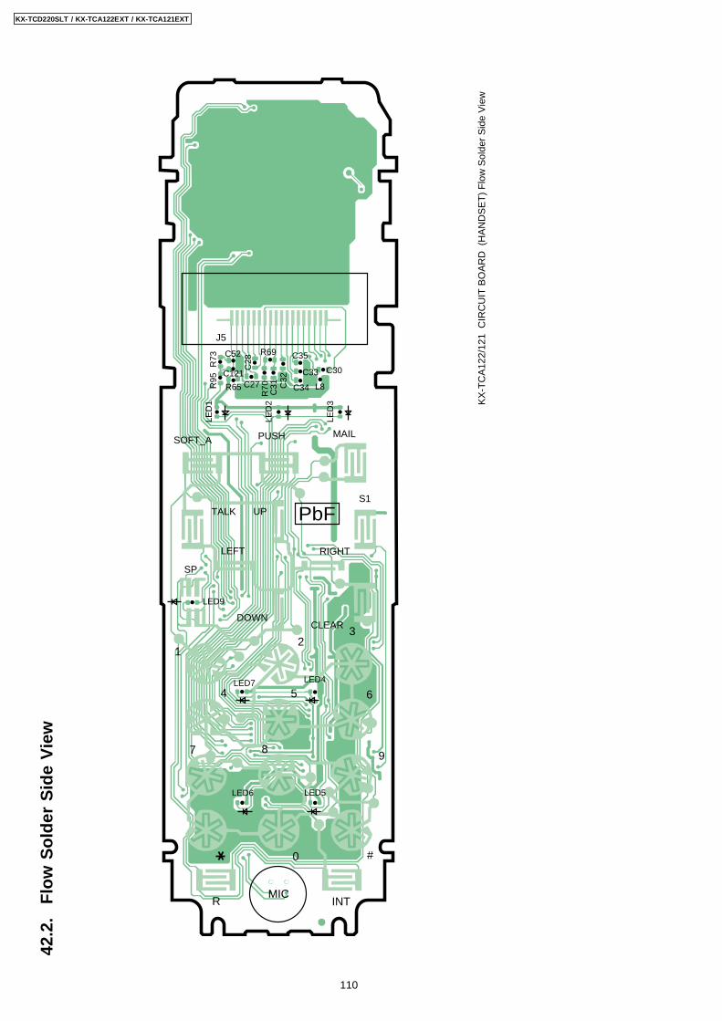
42.2
. F
low
So
lder
Sid
eV
iew
SOFT_A PUSH
J5
CLEAR
PbFUPS1
SP
DOWN
RIGHTLEFT
12
3
65
7
0
LED6 LED5
#
R
4
98
INTMIC
TALK
LED7 LED4
LED9
LED
1
LED
2
LED
3
R95
R70 C31 C
32
C28R73 C52
C30
C35
C33
C34 L8
R69
R65
C121C27
KX
-TC
A12
2/12
1 C
IRC
UIT
BO
AR
D (
HA
ND
SE
T)
Flo
w S
olde
r S
ide
Vie
w
KX-TCD220SLT / KX-TCA122EXT / KX-TCA121EXT
110

43 CIRCUIT BOARD (CHARGER UNIT)43.1. Component View
J1
PQUP11305ZD1
CIRCUIT BOARD (CHARGER UNIT) Component View
D1
A
43.2. Flow Solder Side View
TP3
TP2
TP1
D11
WHITE
BLUE
R12
PbF
R11
R1
R2
TP4
PQUP11305Z
CIRCUIT BOARD (CHARGER UNIT) Flow Solder Side View
A
111
KX-TCD220SLT / KX-TCA122EXT / KX-TCA121EXT
A.I./SKXTCD220SLTKXTCA122EXTKXTCA121EXT