Embed Size (px)
Citation preview
ORDER NO. KM40106816C7F11
Telephone Equipment
KX-TC1503B / KX-TC1503W900MHz Digital Cordless Answering System
Black VersionWhite Version
(for U.S.A.)(for Panama)
SPECIFICATIONS
2001 Kyushu Matsushita Electric Co., Ltd. All rights reserved. Unauthorized copying and distribution is a violation of law.
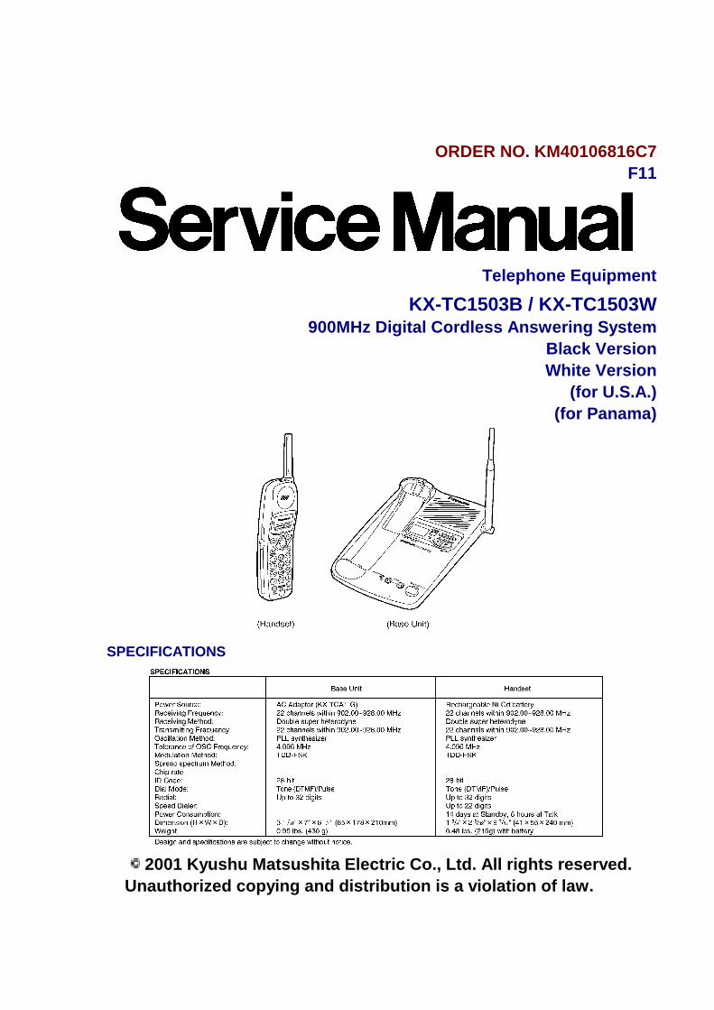
1. STANDARD BATTERY LIFEBattery ChargePlace the headset on the base unit and charge the battery for about 15 hours before initial use.- The IN USE/CHARGE/HOLD indicator lights.
RechargeWhen the RECHARGE indicator flashes, or the unit beeps intermittently, recharge the battery for about 15 hours.- If you DO NOT recharge the handset battery for more than 15
minutes, the RECHARGE indicator will continue to flash.
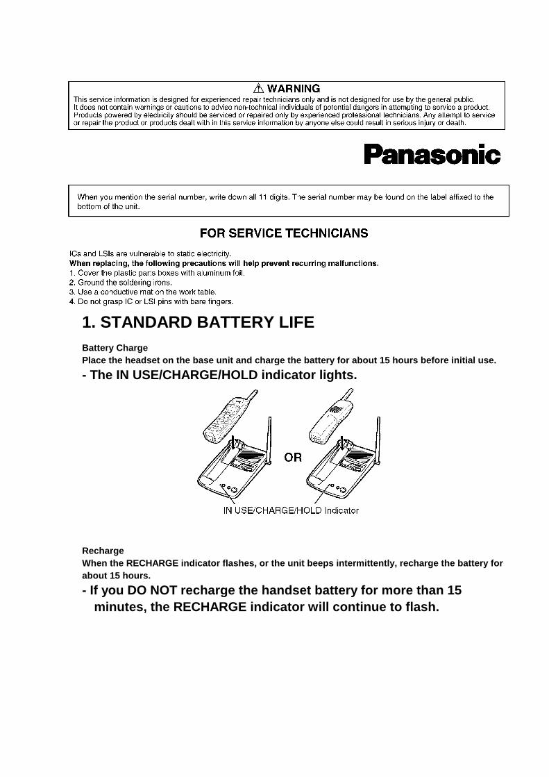
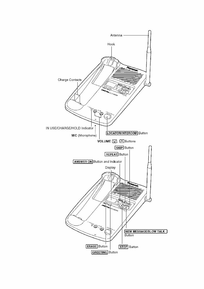
2. LOCATION OF CONTROLS2.1. Base unit
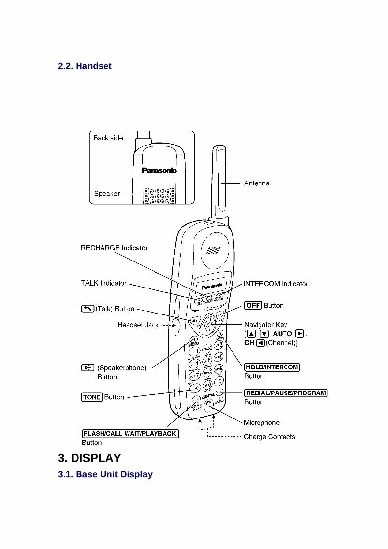
2.2. Handset
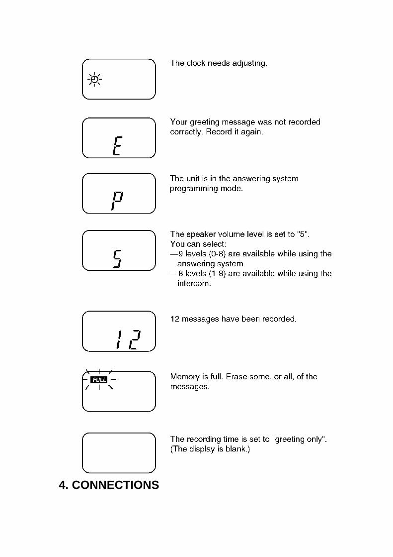
3. DISPLAY3.1. Base Unit Display
4. CONNECTIONS
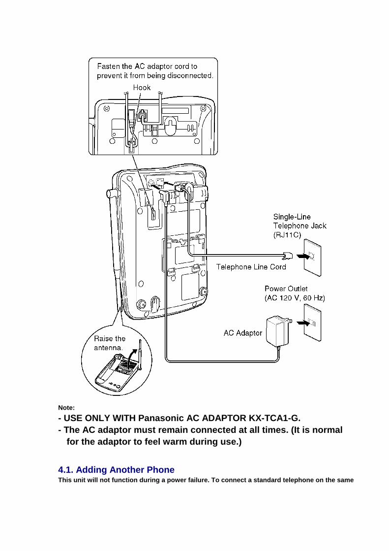
Note:- USE ONLY WITH Panasonic AC ADAPTOR KX-TCA1-G.- The AC adaptor must remain connected at all times. (It is normal
for the adaptor to feel warm during use.)
4.1. Adding Another PhoneThis unit will not function during a power failure. To connect a standard telephone on the same
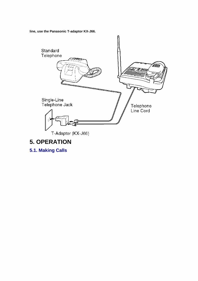
line, use the Panasonic T-adaptor KX-J66.
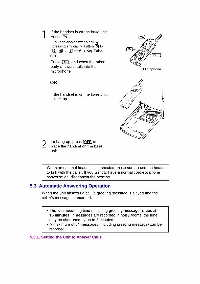
5. OPERATION5.1. Making Calls

5.2. Answering Calls
5.3. Automatic Answering Operation
5.3.1. Setting the Unit to Answer Calls

5.4. Listening to Messages
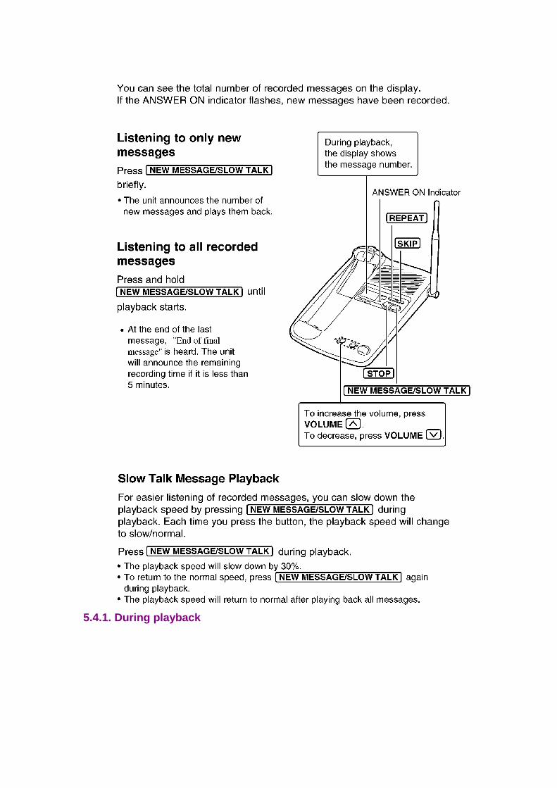
5.4.1. During playback
5.5. FLASH Button
6. DISASSEMBLY INSTRUCTIONS
Shown in Fig.- To Remove Remove1 Lower Cabinet Screws (2.6 X 12).....(A) X 52 Main P.C. Board Remove the P.C. Board3 Antenna Screw (2.6 X 12).....(B) X 1
Speaker Screws (3 X 8).....(C) X 34 Battery Cover Remove the Battery Cover5 Rear Cabinet Screws (2.6 X 12).....(D) X 26 Rear Cabinet Remove the Rear Cabinet7 Main P.C. Board Screw (2.6 × 12).....(E) × 1
Screws (2.6 × 10).....(F) × 2 Remove the lead
Remove the P.C. Board
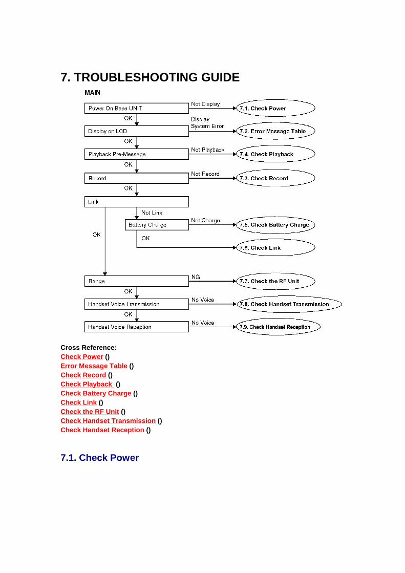
7. TROUBLESHOOTING GUIDE
Cross Reference:Check Power ()Error Message Table ()Check Record ()Check Playback ()Check Battery Charge ()Check Link ()Check the RF Unit ()Check Handset Transmission ()Check Handset Reception ()
7.1. Check Power
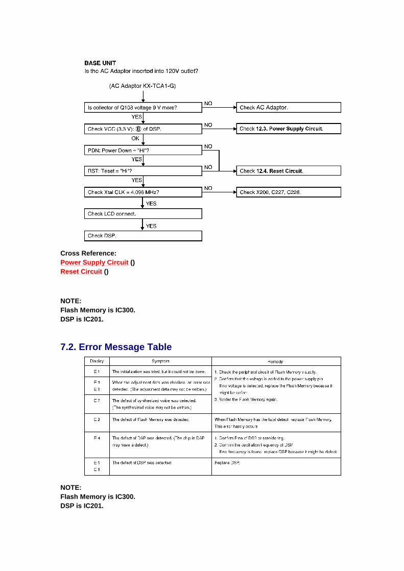
Cross Reference:Power Supply Circuit ()Reset Circuit ()
NOTE: Flash Memory is IC300.DSP is IC201.
7.2. Error Message Table
NOTE: Flash Memory is IC300.DSP is IC201.
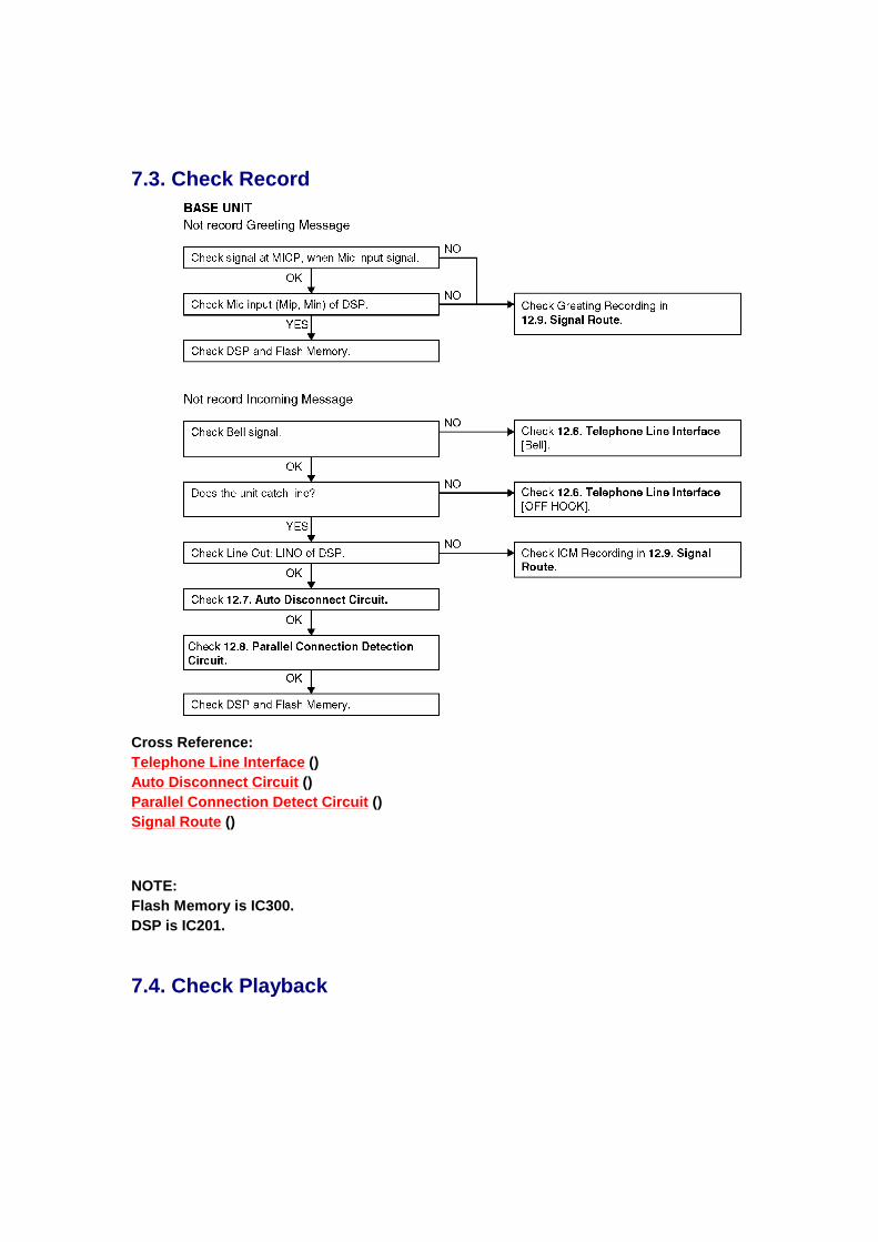
7.3. Check Record
Cross Reference:Telephone Line Interface ()Auto Disconnect Circuit ()Parallel Connection Detect Circuit ()Signal Route ()
NOTE: Flash Memory is IC300.DSP is IC201.
7.4. Check Playback
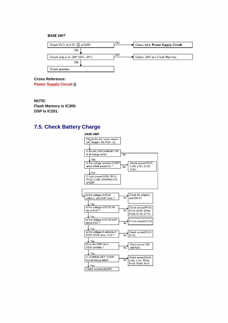
Cross Reference:Power Supply Circuit ()
NOTE: Flash Memory is IC300.DSP is IC201.
7.5. Check Battery Charge
NOTE: Flash Memory is IC300.DSP is IC201.
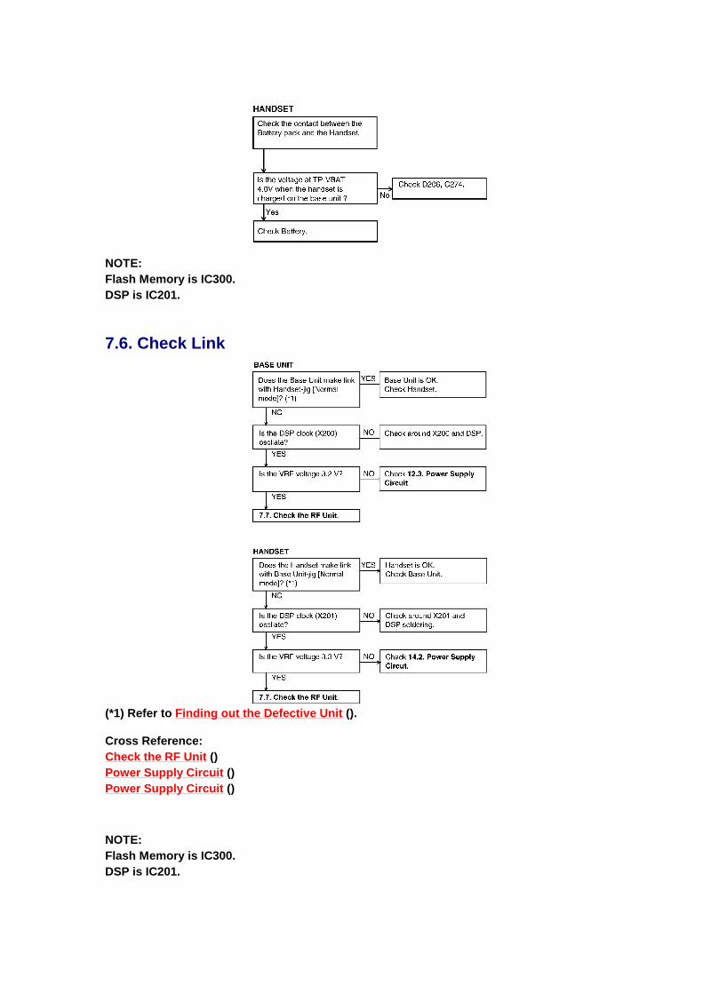
7.6. Check Link
(*1) Refer to Finding out the Defective Unit ().
Cross Reference:Check the RF Unit ()Power Supply Circuit ()Power Supply Circuit ()
NOTE: Flash Memory is IC300.DSP is IC201.
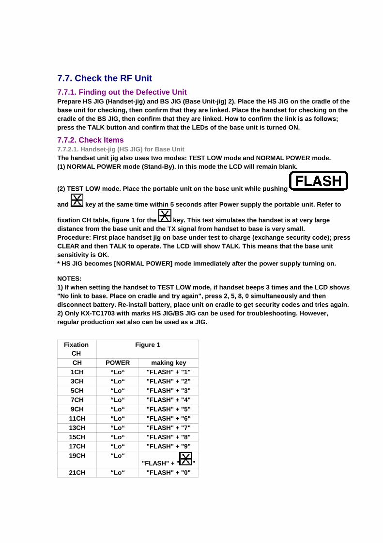
7.7. Check the RF Unit7.7.1. Finding out the Defective UnitPrepare HS JIG (Handset-jig) and BS JIG (Base Unit-jig) 2). Place the HS JIG on the cradle of the base unit for checking, then confirm that they are linked. Place the handset for checking on the cradle of the BS JIG, then confirm that they are linked. How to confirm the link is as follows; press the TALK button and confirm that the LEDs of the base unit is turned ON.
7.7.2. Check Items7.7.2.1. Handset-jig (HS JIG) for Base UnitThe handset unit jig also uses two modes: TEST LOW mode and NORMAL POWER mode.(1) NORMAL POWER mode (Stand-By). In this mode the LCD will remain blank.
(2) TEST LOW mode. Place the portable unit on the base unit while pushing
and key at the same time within 5 seconds after Power supply the portable unit. Refer to
fixation CH table, figure 1 for the key. This test simulates the handset is at very large distance from the base unit and the TX signal from handset to base is very small.Procedure: First place handset jig on base under test to charge (exchange security code); press CLEAR and then TALK to operate. The LCD will show TALK. This means that the base unit sensitivity is OK.* HS JIG becomes [NORMAL POWER] mode immediately after the power supply turning on.
NOTES:1) If when setting the handset to TEST LOW mode, if handset beeps 3 times and the LCD shows "No link to base. Place on cradle and try again", press 2, 5, 8, 0 simultaneously and then disconnect battery. Re-install battery, place unit on cradle to get security codes and tries again.2) Only KX-TC1703 with marks HS JIG/BS JIG can be used for troubleshooting. However, regular production set also can be used as a JIG.
Fixation CH
Figure 1
CH POWER making key1CH “Lo“ "FLASH" + "1"3CH “Lo“ "FLASH" + "2"5CH “Lo“ "FLASH" + "3"7CH “Lo“ "FLASH" + "4"9CH “Lo“ "FLASH" + "5"11CH “Lo“ "FLASH" + "6"13CH “Lo“ "FLASH" + "7"15CH “Lo“ "FLASH" + "8"17CH “Lo“ "FLASH" + "9"19CH “Lo“
"FLASH" + " "21CH “Lo“ "FLASH" + "0"
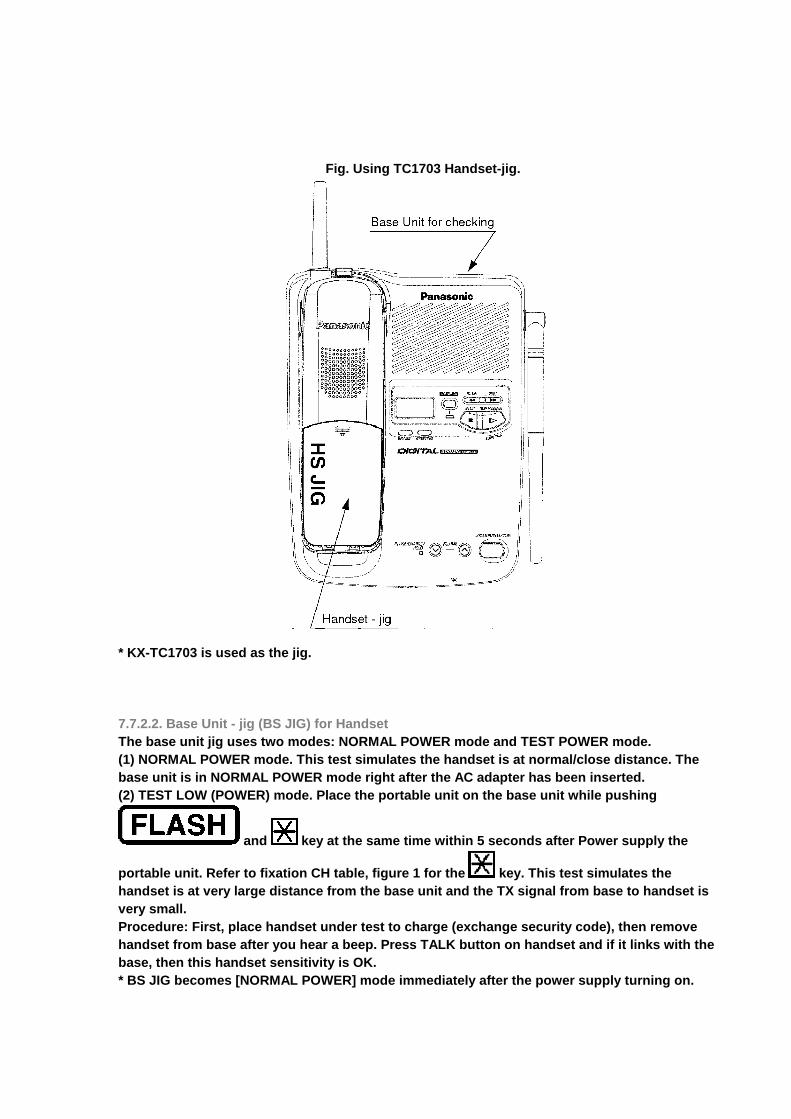
Fig. Using TC1703 Handset-jig.
* KX-TC1703 is used as the jig.
7.7.2.2. Base Unit - jig (BS JIG) for HandsetThe base unit jig uses two modes: NORMAL POWER mode and TEST POWER mode.(1) NORMAL POWER mode. This test simulates the handset is at normal/close distance. The base unit is in NORMAL POWER mode right after the AC adapter has been inserted.(2) TEST LOW (POWER) mode. Place the portable unit on the base unit while pushing
and key at the same time within 5 seconds after Power supply the
portable unit. Refer to fixation CH table, figure 1 for the key. This test simulates the handset is at very large distance from the base unit and the TX signal from base to handset is very small.Procedure: First, place handset under test to charge (exchange security code), then remove handset from base after you hear a beep. Press TALK button on handset and if it links with the base, then this handset sensitivity is OK.* BS JIG becomes [NORMAL POWER] mode immediately after the power supply turning on.
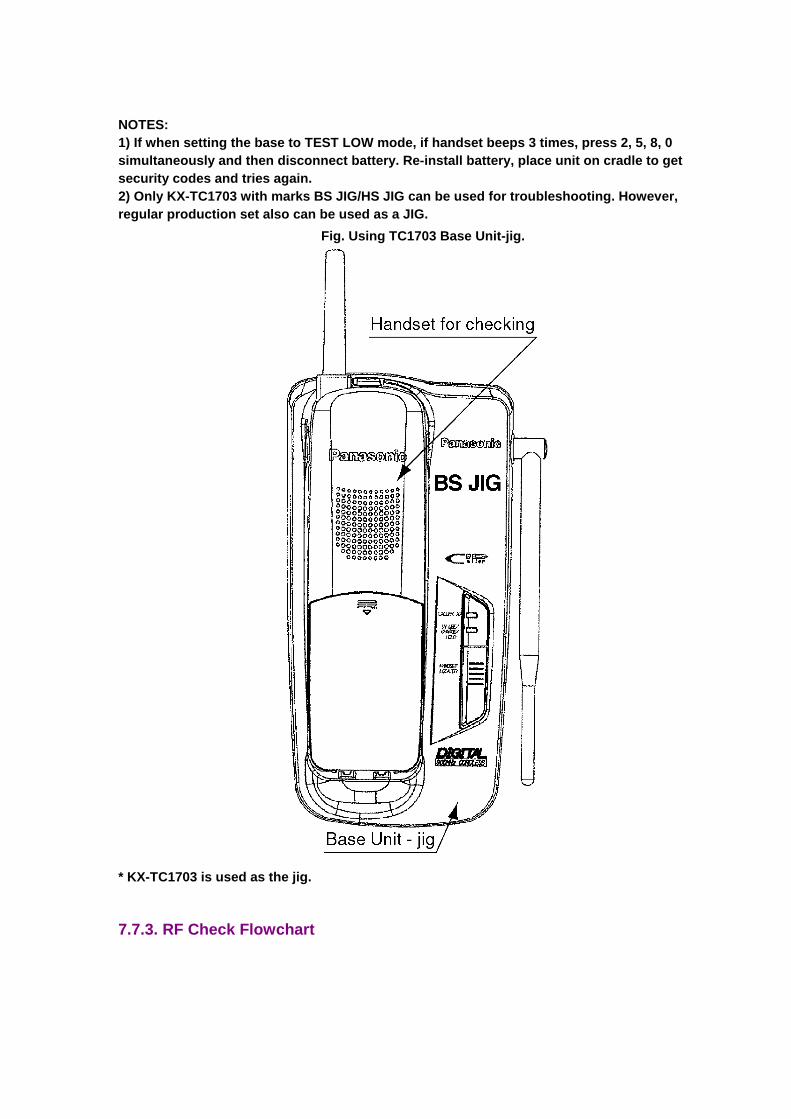
NOTES:1) If when setting the base to TEST LOW mode, if handset beeps 3 times, press 2, 5, 8, 0 simultaneously and then disconnect battery. Re-install battery, place unit on cradle to get security codes and tries again.2) Only KX-TC1703 with marks BS JIG/HS JIG can be used for troubleshooting. However, regular production set also can be used as a JIG.
Fig. Using TC1703 Base Unit-jig.
* KX-TC1703 is used as the jig.
7.7.3. RF Check Flowchart
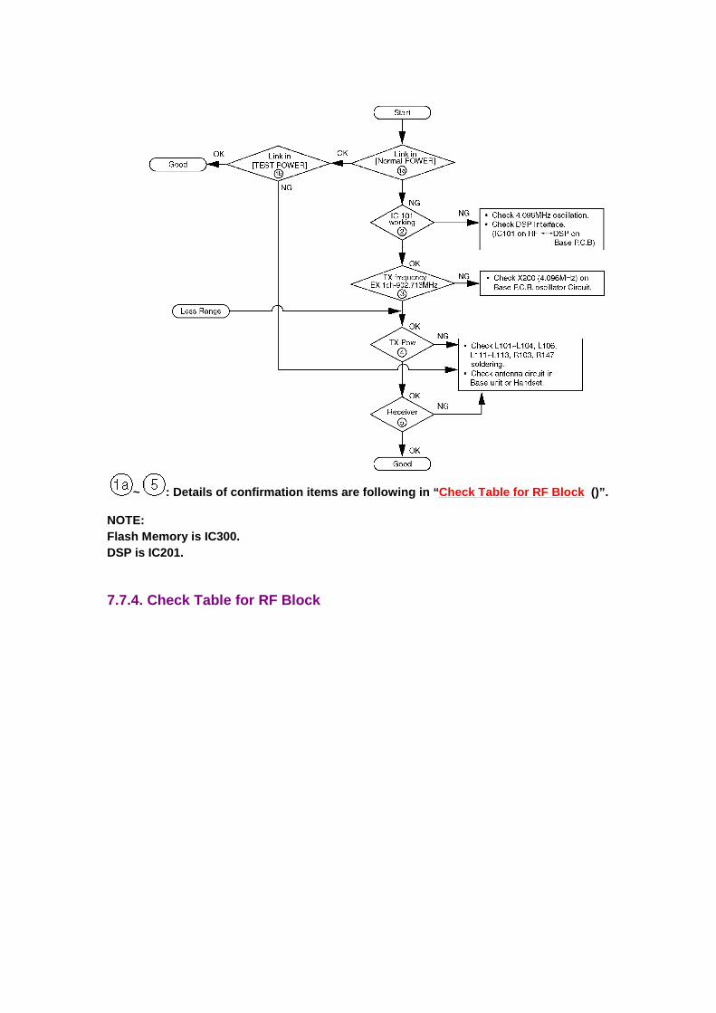
~ : Details of confirmation items are following in “Check Table for RF Block ()”.
NOTE: Flash Memory is IC300.DSP is IC201.
7.7.4. Check Table for RF Block
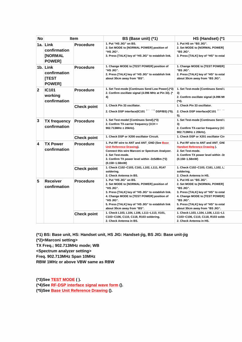
No Item BS (Base unit) (*1) HS (Handset) (*1)1a. Link
confirmation [NORMAL POWER]
Procedure 1. Put “HS JIG” on BS.2. Set MODE to [NORMAL POWER] position of “HS JIG“.3. Press [TALK] key of “HS JIG” to establish link.
1. Put HS on “BS JIG”.2. Set MODE to [NORMAL POWER] position “BS JIG“.3. Press [TALK] key of “HS” to establish
1b. Link confirmation [TEST POWER]
Procedure 1. Change MODE to [TEST POWER] position of “HS JIG”.2. Press [TALK] key of “HS JIG” to establish link about 30cm away from “BS”.
1. Change MODE to [TEST POWER] “BS JIG”.2. Press [TALK] key of “HS“ to establish about 30cm away from “BS JIG”.
2 IC101 working confirmation
Procedure 1. Set Test-mode [Continuos Send Low Power].(*3)2. Confirm oscillate signal (4.096 MHz at Pin 33). (*4)
1. Set Test-mode [Continuos Send Low 3)2. Confirm oscillate signal (4.096 MHz (*4).
Check point 1. Check Pin 33 oscillator.
2. Check DSP interface(IC101 DSP/BS) (*5).
1. Check Pin 33 oscillator.
2. Check DSP interface(IC101 5).
3 TX frequency confirmation
Procedure 1. Set Test-model [Continuos Send].(*3)2. Confirm TX-carrier frequency (1CH = 902.713MHz ± 20kHz).
1. Set Test-mode [Continuos Send Low 3)2. Confirm TX-carrier frequency (1CH 902.713MHz ± 20kHz).
Check point 1. Check DSP or X200 oscillator Circuit. 1. Check DSP or X201 oscillator Circuit.
4 TX Power confirmation
Procedure 1. Put RF wire to ANT and ANT_GND (See Base Unit Reference Drawing).Connect this wire Marconi or Spectrum Analyzer.2. Set Test-mode.3. Confirm TX power level within -3±5dBm (*2)(0.158~1.58mW)
1. Put RF wire to ANT and ANT_GND Handset Reference Drawing ).2. Set Test-mode.3. Confirm TX power level within -3±(0.158~1.58mW)
Check point 1. Check C102~C103, C161, L102, L111, R147 soldering.2. Check Antenna in BS.
1. Check C102~C103, C161, L102, L111, soldering.2. Check Antenna in HS.
5 Receiver confirmation
Procedure 1. Put “HS JIG” on BS.2. Set MODE to [NORMAL POWER] position of “HS JIG”.3. Press [TALK] key of “HS JIG“ to establish link.4. Change MODE to [TEST POWER] position of “HS JIG“.5. Press [TALK] key of “HS JIG” to establish link about 30cm away from “BS”.
1. Put HS on “BS JIG”.2. Set MODE to [NORMAL POWER] position “BS JIG”.3. Press [TALK] key of “HS” to establish 4. Change MODE to [TEST POWER] “BS JIG”.5. Press [TALK] key of “HS” to establish about 30cm away from “BS JIG“.
Check point 1. Check L103, L104, L106, L111~L113, X101, C103~C106, C110, C118, R103 soldering.2. Check Antenna in BS.
1. Check L103, L104, L106, L111~L113, C103~C106, C110, C118, R103 soldering.2. Check Antenna in HS.
(*1) BS: Base unit, HS: Handset unit, HS JIG: Handset-jig, BS JIG: Base unit-jig(*2)<Marconi setting> TX Freq.; 902.713MHz mode; WB<Spectrum analyzer setting>Freq. 902.713MHz Span 10MHzRBW 1MHz or above VBW same as RBW
(*3)See TEST MODE ( ).(*4)See RF-DSP interface signal wave form ().(*5)See Base Unit Reference Drawing ().
NOTE: Flash Memory is IC300.DSP is IC201.
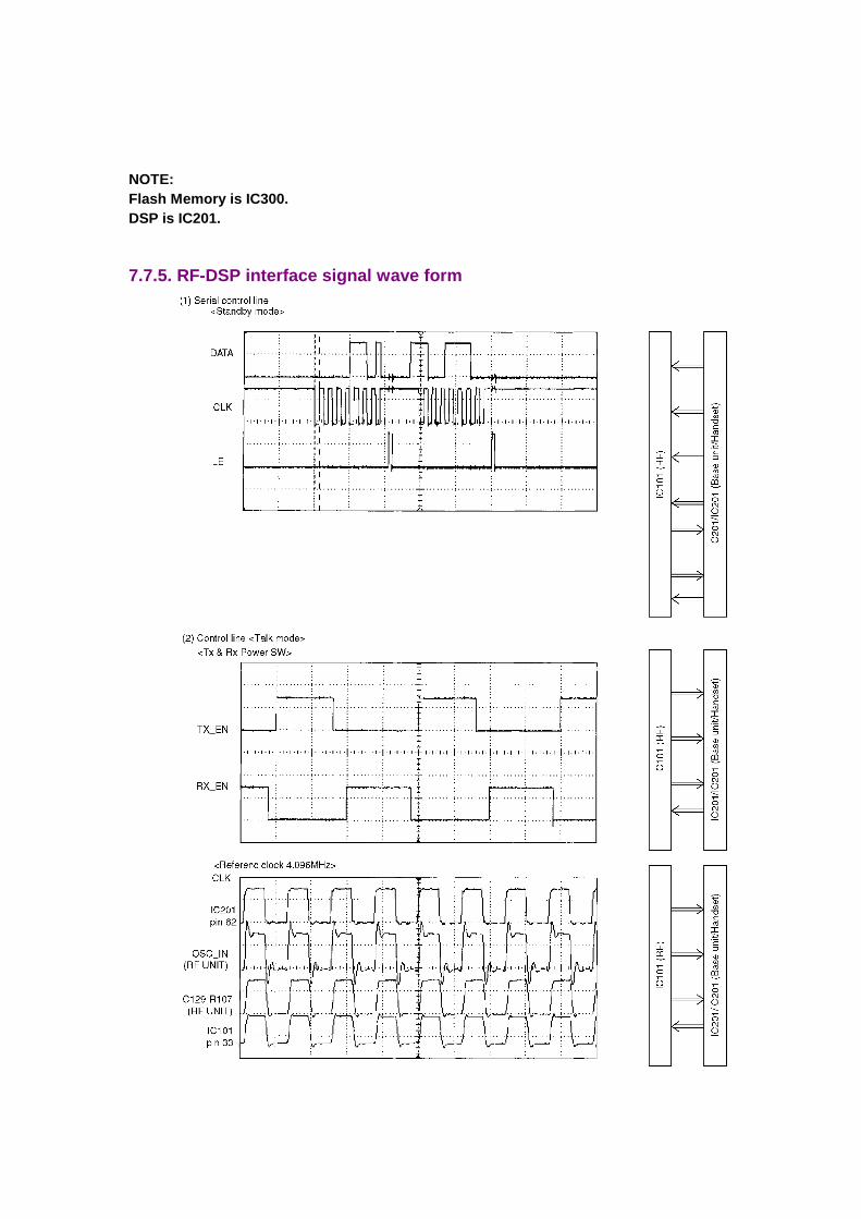
7.7.5. RF-DSP interface signal wave form
7.8. Check Handset Transmission
Cross Reference:Signal Route ().
7.9. Check Handset Reception
Cross Reference:Signal Route ().
NOTE: When checking the RF UNIT, Refer to Check the RF Unit ()
8. TEST MODE8.1. Test mode flow chart for Base Unit

(*1) See Base Unit Reference Drawing () - Should return to OPEN after entering the Test mode.(*2) It shows whether the telephone line is connected or not. -ON: OFF HOOK.-OFF: ON HOOK
8.2. TAM Test mode flow chart
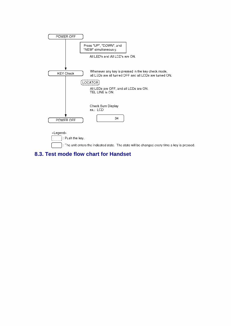
8.3. Test mode flow chart for Handset
(*1) See Handset Reference Drawing ( ).---Should return to OPEN after entering the Test mode.
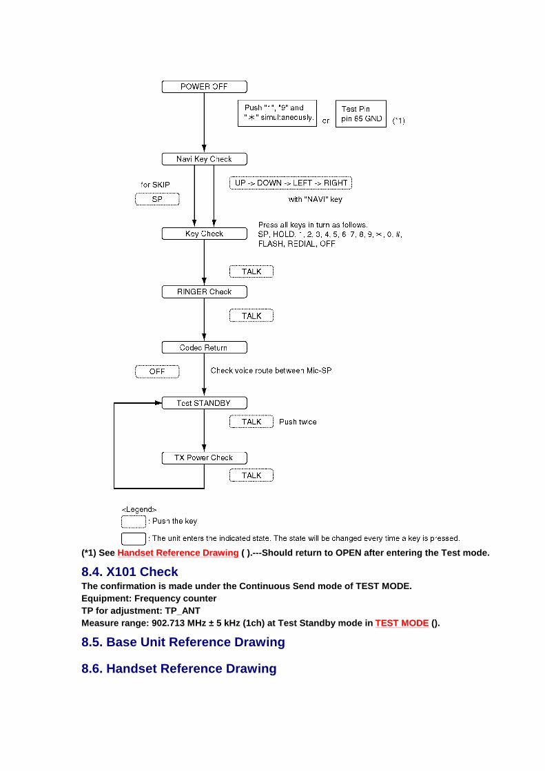
8.4. X101 CheckThe confirmation is made under the Continuous Send mode of TEST MODE.Equipment: Frequency counterTP for adjustment: TP_ANTMeasure range: 902.713 MHz ± 5 kHz (1ch) at Test Standby mode in TEST MODE ().
8.5. Base Unit Reference Drawing
8.6. Handset Reference Drawing
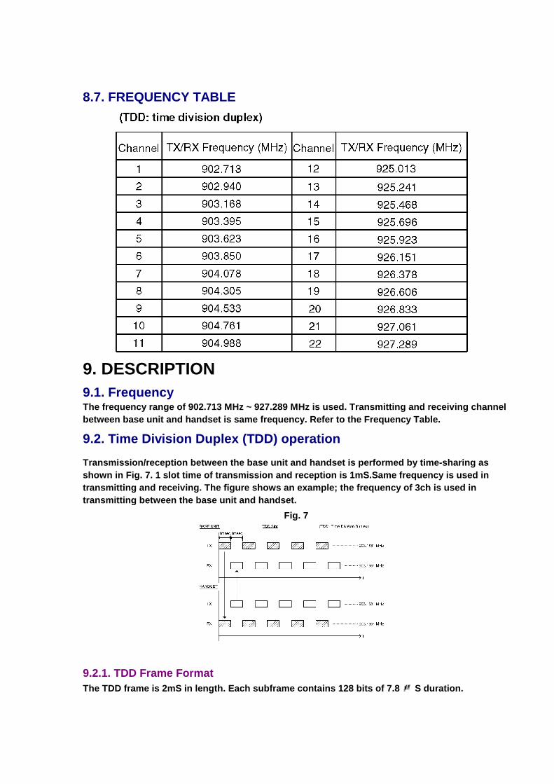
8.7. FREQUENCY TABLE
9. DESCRIPTION9.1. FrequencyThe frequency range of 902.713 MHz ~ 927.289 MHz is used. Transmitting and receiving channel between base unit and handset is same frequency. Refer to the Frequency Table.
9.2. Time Division Duplex (TDD) operationTransmission/reception between the base unit and handset is performed by time-sharing as shown in Fig. 7. 1 slot time of transmission and reception is 1mS.Same frequency is used in transmitting and receiving. The figure shows an example; the frequency of 3ch is used in transmitting between the base unit and handset.
Fig. 7
9.2.1. TDD Frame FormatThe TDD frame is 2mS in length. Each subframe contains 128 bits of 7.8 S duration.
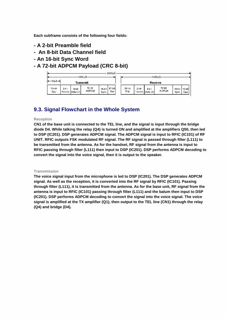
Each subframe consists of the following four fields:
- A 2-bit Preamble field- An 8-bit Data Channel field- An 16-bit Sync Word- A 72-bit ADPCM Payload (CRC 8-bit)
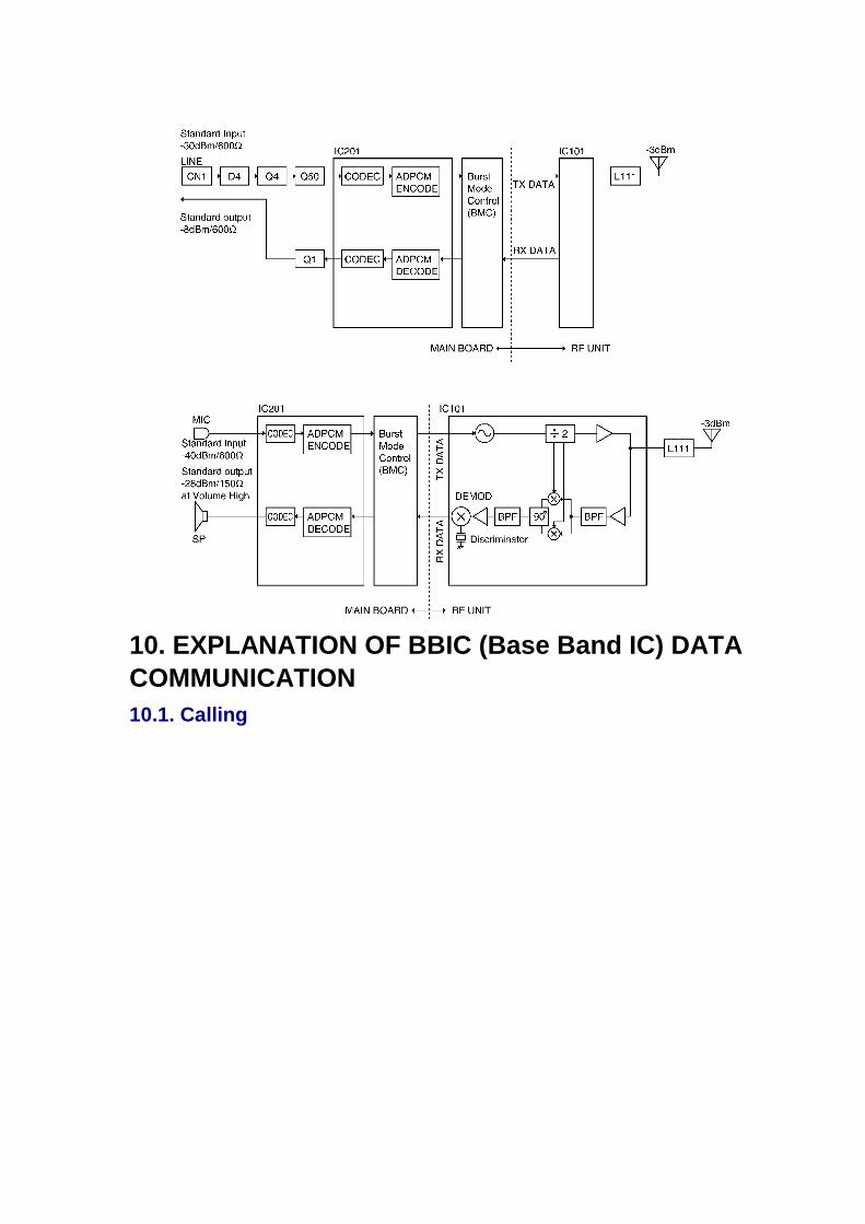
9.3. Signal Flowchart in the Whole SystemReceptionCN1 of the base unit is connected to the TEL line, and the signal is input through the bridge diode D4. While talking the relay (Q4) is turned ON and amplified at the amplifiers Q50, then led to DSP (IC201). DSP generates ADPCM signal. The ADPCM signal is input to RFIC (IC101) of RF UNIT. RFIC outputs FSK modulated RF signal. The RF signal is passed through filter (L111) to be transmitted from the antenna. As for the handset, RF signal from the antenna is input to RFIC passing through filter (L111) then input to DSP (IC201). DSP performs ADPCM decoding to convert the signal into the voice signal, then it is output to the speaker.
TransmissionThe voice signal input from the microphone is led to DSP (IC201). The DSP generates ADPCM signal. As well as the reception, it is converted into the RF signal by RFIC (IC101). Passing through filter (L111), it is transmitted from the antenna. As for the base unit, RF signal from the antenna is input to RFIC (IC101) passing through filter (L111) and the balum then input to DSP (IC201). DSP performs ADPCM decoding to convert the signal into the voice signal. The voice signal is amplified at the TX amplifier (Q1), then output to the TEL line (CN1) through the relay (Q4) and bridge (D4).
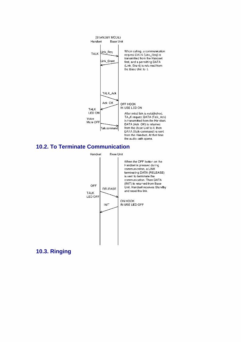
10. EXPLANATION OF BBIC (Base Band IC) DATA COMMUNICATION10.1. Calling
10.2. To Terminate Communication
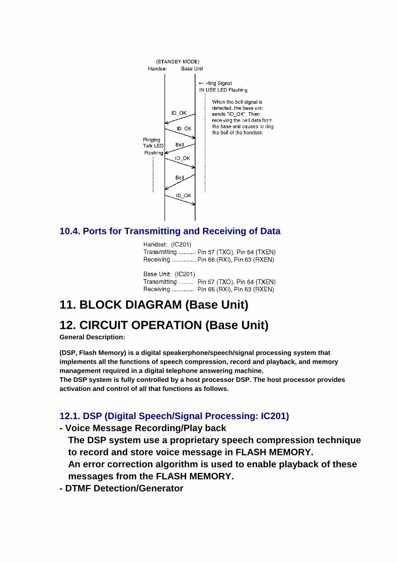
10.3. Ringing
10.4. Ports for Transmitting and Receiving of Data
11. BLOCK DIAGRAM (Base Unit)12. CIRCUIT OPERATION (Base Unit)General Description:
(DSP, Flash Memory) is a digital speakerphone/speech/signal processing system that implements all the functions of speech compression, record and playback, and memory management required in a digital telephone answering machine.The DSP system is fully controlled by a host processor DSP. The host processor provides activation and control of all that functions as follows.
12.1. DSP (Digital Speech/Signal Processing: IC201)- Voice Message Recording/Play back
The DSP system use a proprietary speech compression technique to record and store voice message in FLASH MEMORY.An error correction algorithm is used to enable playback of these messages from the FLASH MEMORY.
- DTMF Detection/Generator
The DTMF detection is implemented by the DSP system in software. The DTMF detection is performed during Record, Playback, and Line Monitoring modes of operation.When the DTMF data from the Handset is received, the DTMF signal is output.
- Synthesized Voice (Pre-recorded message)The DSP implements synthesized Voice, utilizing the built in speech detector and an FLASH MEMORY, which stored the vocabulary.
- Analog SwitchingThe voice signal from telephone line is transmitted to the speaker or the voice signal from speakerphone microphone is transmitted to the Telephone line, etc. They are determined by the signal path route operation of voice signal.
- Block Interface CircuitRF unit, LED, Key scan, Speaker, Microphone, Telephone line, LCD
12.2. Flash Memory (IC300)Following information data is stored.- Voice signal
ex: Pre-recorded Greeting message, Incoming message- Telephone number, etc.
ex: Telephone Directory number, ID code - Settings
ex: message numbers, pulse tone dial12.3. Power Supply CircuitFunction:The power supply voltage from AC adaptor is converted to the desired voltage of each block.Circuit Operation:This unit supplies the voltage to each block as shown below.
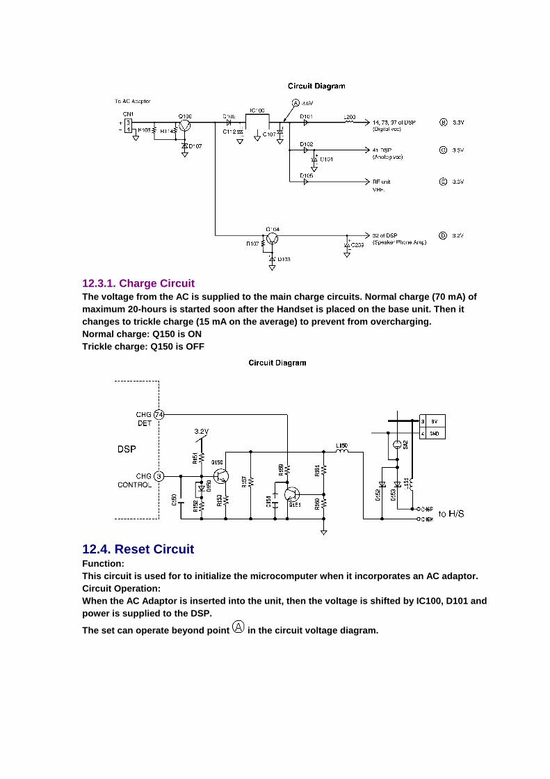
12.3.1. Charge CircuitThe voltage from the AC is supplied to the main charge circuits. Normal charge (70 mA) of maximum 20-hours is started soon after the Handset is placed on the base unit. Then it changes to trickle charge (15 mA on the average) to prevent from overcharging.Normal charge: Q150 is ONTrickle charge: Q150 is OFF
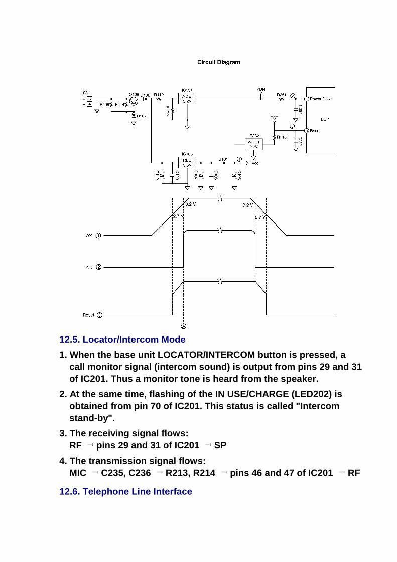
12.4. Reset CircuitFunction:This circuit is used for to initialize the microcomputer when it incorporates an AC adaptor.Circuit Operation:When the AC Adaptor is inserted into the unit, then the voltage is shifted by IC100, D101 and power is supplied to the DSP.
The set can operate beyond point in the circuit voltage diagram.
12.5. Locator/Intercom Mode1. When the base unit LOCATOR/INTERCOM button is pressed, a
call monitor signal (intercom sound) is output from pins 29 and 31 of IC201. Thus a monitor tone is heard from the speaker.
2. At the same time, flashing of the IN USE/CHARGE (LED202) is obtained from pin 70 of IC201. This status is called "Intercom stand-by".
3. The receiving signal flows:RF pins 29 and 31 of IC201 SP
4. The transmission signal flows:MIC C235, C236 R213, R214 pins 46 and 47 of IC201 RF
12.6. Telephone Line Interface
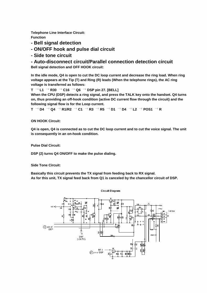
Telephone Line Interface Circuit:Function- Bell signal detection- ON/OFF hook and pulse dial circuit- Side tone circuit- Auto-disconnect circuit/Parallel connection detection circuitBell signal detection and OFF HOOK circuit:
In the idle mode, Q4 is open to cut the DC loop current and decrease the ring load. When ring voltage appears at the Tip (T) and Ring (R) leads (When the telephone rings), the AC ring voltage is transferred as follows:T L1 R30 C16 Q6 DSP pin 27. [BELL]When the CPU (DSP) detects a ring signal, and press the TALK key onto the handset. Q4 turns on, thus providing an off-hook condition (active DC current flow through the circuit) and the following signal flow is for the Loop current.T D4 Q4 R1/R2 C1 R3 R5 D1 D4 L2 POS1 R
ON HOOK Circuit:
Q4 is open, Q4 is connected as to cut the DC loop current and to cut the voice signal. The unit is consequently in an on-hook condition.
Pulse Dial Circuit:
DSP (2) turns Q4 ON/OFF to make the pulse dialing.
Side Tone Circuit:
Basically this circuit prevents the TX signal from feeding back to RX signal.As for this unit, TX signal feed back from Q1 is canceled by the chancellor circuit of DSP.
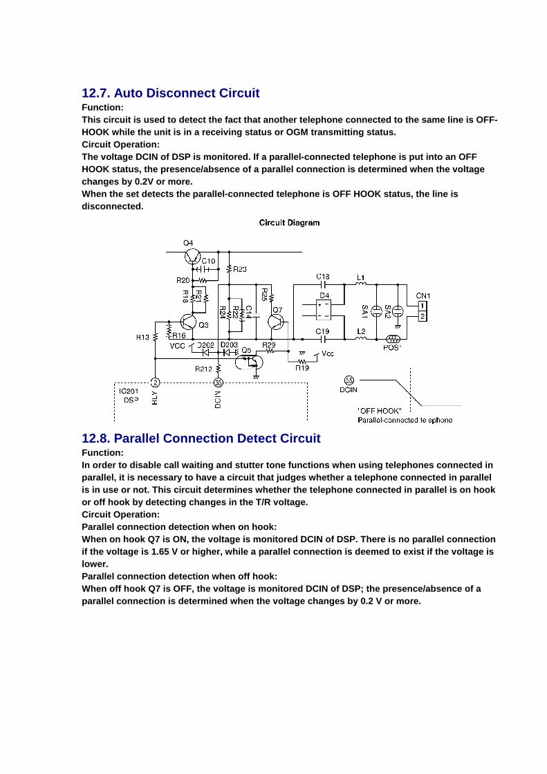
12.7. Auto Disconnect CircuitFunction:This circuit is used to detect the fact that another telephone connected to the same line is OFF-HOOK while the unit is in a receiving status or OGM transmitting status.Circuit Operation:The voltage DCIN of DSP is monitored. If a parallel-connected telephone is put into an OFF HOOK status, the presence/absence of a parallel connection is determined when the voltage changes by 0.2V or more.When the set detects the parallel-connected telephone is OFF HOOK status, the line is disconnected.
12.8. Parallel Connection Detect CircuitFunction:In order to disable call waiting and stutter tone functions when using telephones connected in parallel, it is necessary to have a circuit that judges whether a telephone connected in parallel is in use or not. This circuit determines whether the telephone connected in parallel is on hook or off hook by detecting changes in the T/R voltage.Circuit Operation:Parallel connection detection when on hook:When on hook Q7 is ON, the voltage is monitored DCIN of DSP. There is no parallel connection if the voltage is 1.65 V or higher, while a parallel connection is deemed to exist if the voltage is lower.Parallel connection detection when off hook:When off hook Q7 is OFF, the voltage is monitored DCIN of DSP; the presence/absence of a parallel connection is determined when the voltage changes by 0.2 V or more.
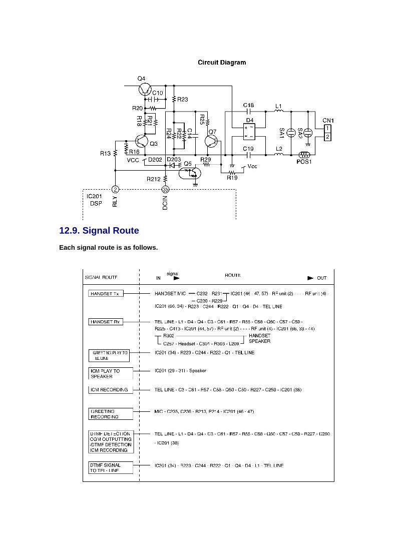
12.9. Signal RouteEach signal route is as follows.
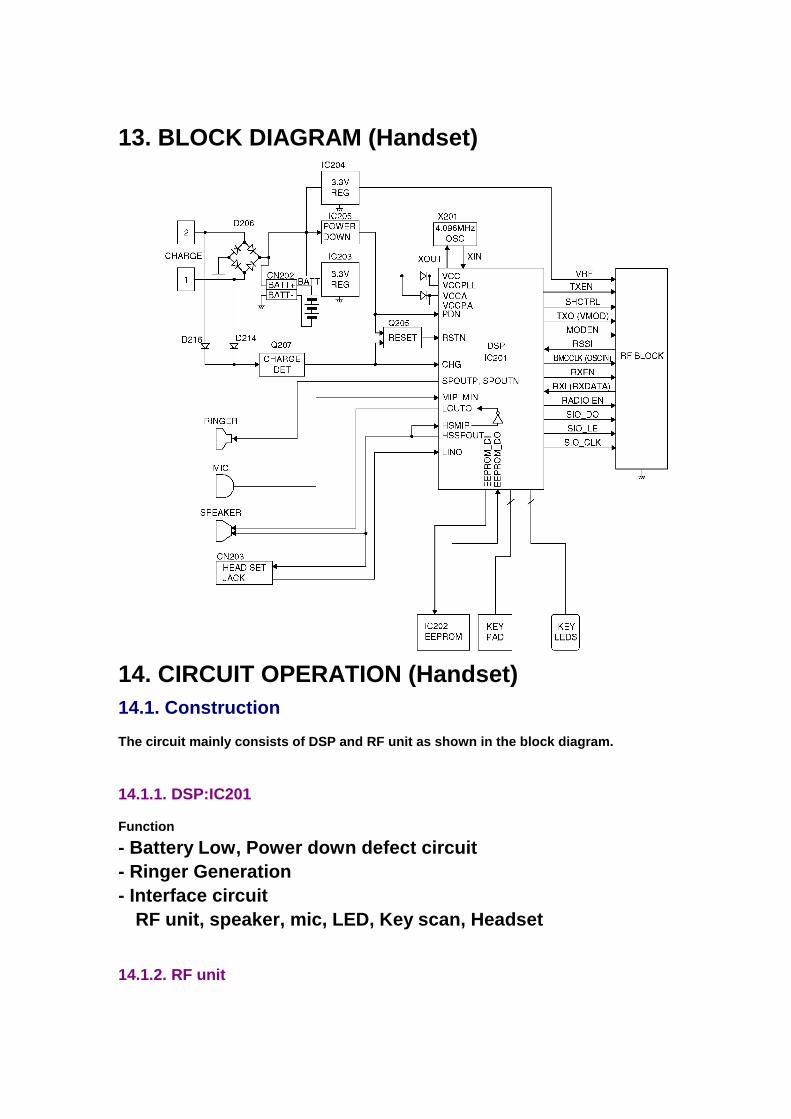
13. BLOCK DIAGRAM (Handset)
14. CIRCUIT OPERATION (Handset)14.1. ConstructionThe circuit mainly consists of DSP and RF unit as shown in the block diagram.
14.1.1. DSP:IC201
Function- Battery Low, Power down defect circuit- Ringer Generation- Interface circuit
RF unit, speaker, mic, LED, Key scan, Headset
14.1.2. RF unit
Mainly voice signal is modulated to RF, or it goes the other way.
14.1.3. EEPROM: IC201
All setting data is stored.ex: ID code, user setting (Flash Time, Tone/Pulse)
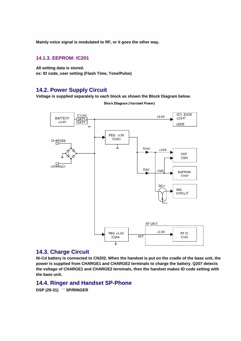
14.2. Power Supply CircuitVoltage is supplied separately to each block as shown the Block Diagram below.
14.3. Charge CircuitNi-Cd battery is connected to CN202. When the handset is put on the cradle of the base unit, the power is supplied from CHARGE1 and CHARGE2 terminals to charge the battery. Q207 detects the voltage of CHARGE1 and CHARGE2 terminals, then the handset makes ID code setting with the base unit.
14.4. Ringer and Handset SP-PhoneDSP (29-31) SP/RINGER
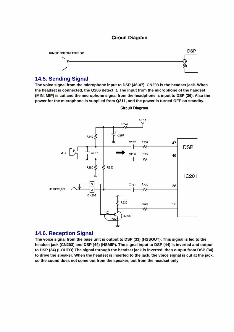
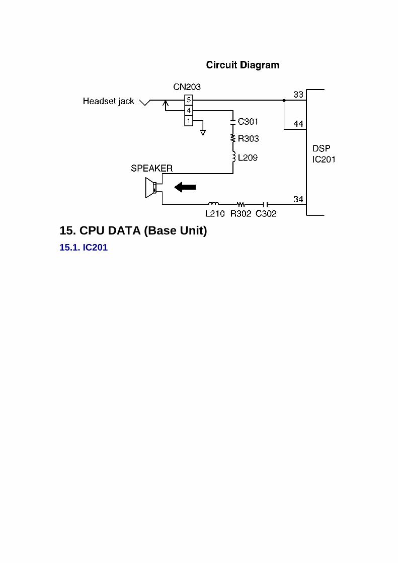
14.5. Sending SignalThe voice signal from the microphone input to DSP (46-47). CN203 is the headset jack. When the headset is connected, the Q206 detect it. The input from the microphone of the handset (MIN, MIP) is cut and the microphone signal from the headphone is input to DSP (36). Also the power for the microphone is supplied from Q211, and the power is turned OFF on standby.
14.6. Reception SignalThe voice signal from the base unit is output to DSP (33) (HSSOUT). This signal is led to the headset jack (CN203) and DSP (44) (HSMIP). The signal input to DSP (44) is inverted and output to DSP (34) (LOUTO).The signal through the headset jack is inverted, then output from DSP (34) to drive the speaker. When the headset is inserted to the jack, the voice signal is cut at the jack, so the sound does not come out from the speaker, but from the headset only.
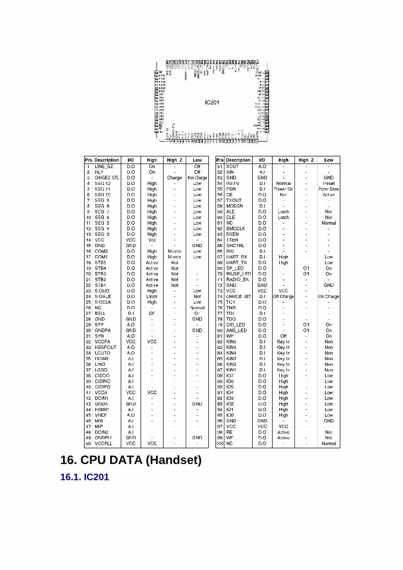
15. CPU DATA (Base Unit)15.1. IC201
16. CPU DATA (Handset)16.1. IC201
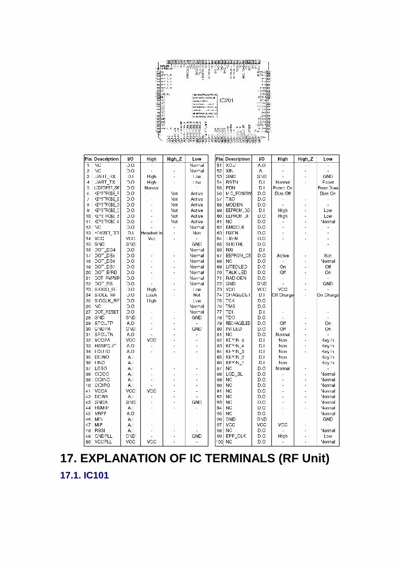
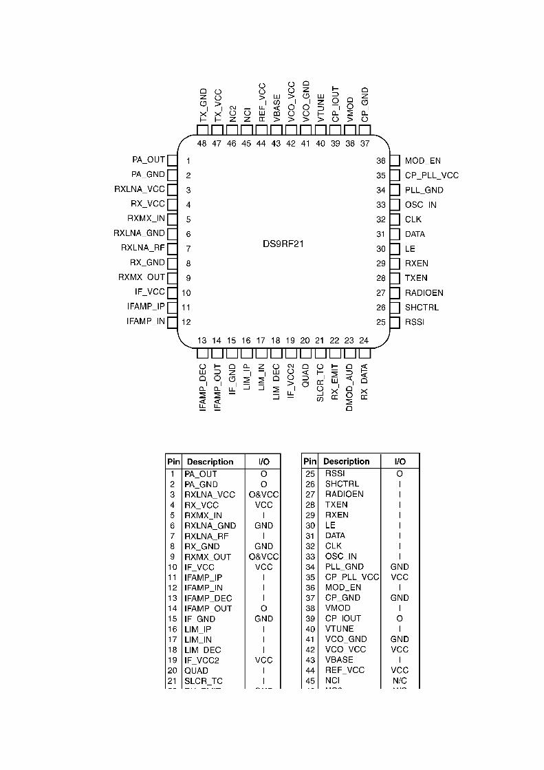
17. EXPLANATION OF IC TERMINALS (RF Unit)17.1. IC101
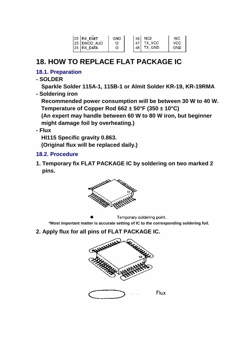
18. HOW TO REPLACE FLAT PACKAGE IC18.1. Preparation- SOLDER
Sparkle Solder 115A-1, 115B-1 or Almit Solder KR-19, KR-19RMA - Soldering iron
Recommended power consumption will be between 30 W to 40 W.Temperature of Copper Rod 662 ± 50°F (350 ± 10°C)(An expert may handle between 60 W to 80 W iron, but beginner might damage foil by overheating.)
- FluxHI115 Specific gravity 0.863.(Original flux will be replaced daily.)
18.2. Procedure1. Temporary fix FLAT PACKAGE IC by soldering on two marked 2
pins.
*Most important matter is accurate setting of IC to the corresponding soldering foil.
2. Apply flux for all pins of FLAT PACKAGE IC.
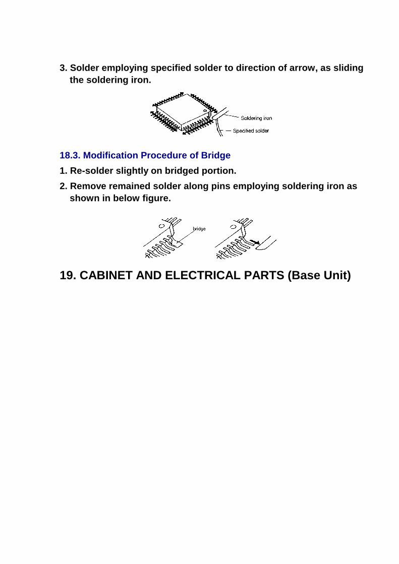
3. Solder employing specified solder to direction of arrow, as sliding the soldering iron.
18.3. Modification Procedure of Bridge1. Re-solder slightly on bridged portion.2. Remove remained solder along pins employing soldering iron as
shown in below figure.
19. CABINET AND ELECTRICAL PARTS (Base Unit)

20. CABINET AND ELECTRICAL PARTS (Handset)
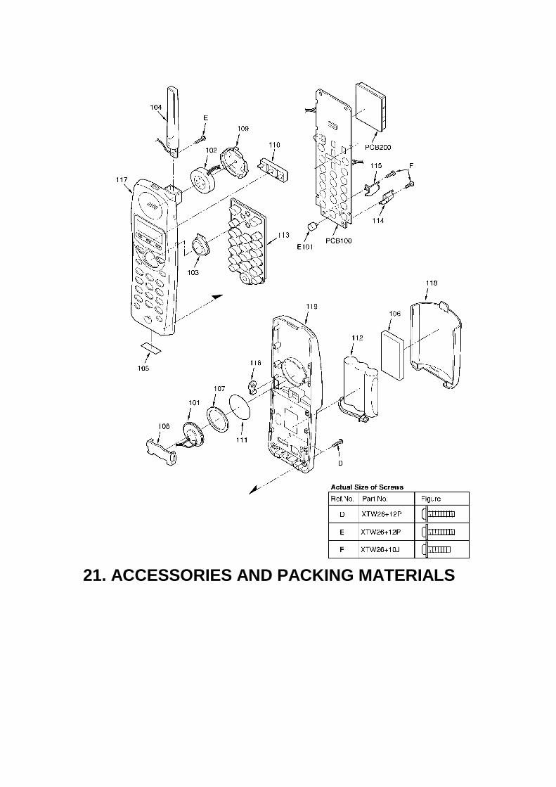
21. ACCESSORIES AND PACKING MATERIALS
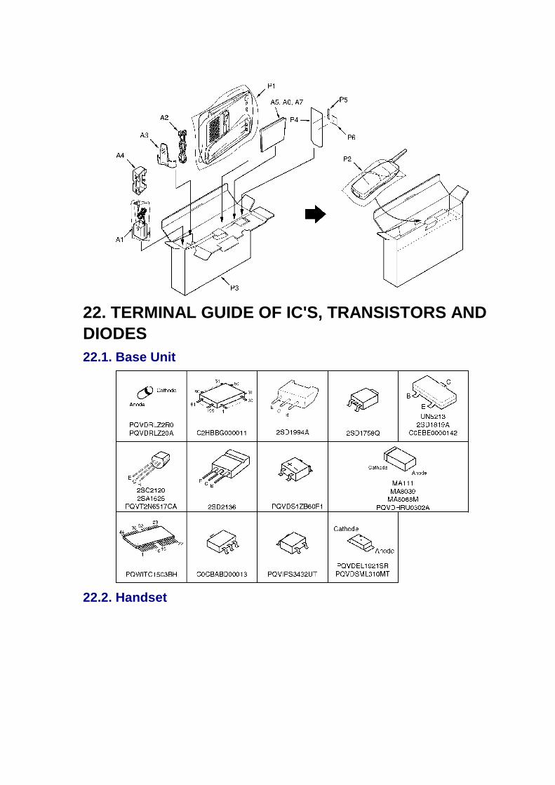
22. TERMINAL GUIDE OF IC'S, TRANSISTORS AND DIODES22.1. Base Unit
22.2. Handset
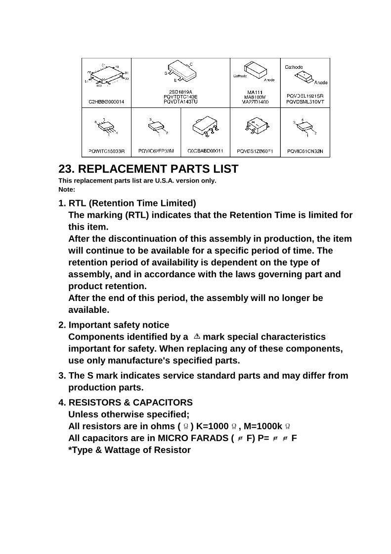
23. REPLACEMENT PARTS LISTThis replacement parts list are U.S.A. version only.Note:
1. RTL (Retention Time Limited)The marking (RTL) indicates that the Retention Time is limited for this item.After the discontinuation of this assembly in production, the item will continue to be available for a specific period of time. The retention period of availability is dependent on the type of assembly, and in accordance with the laws governing part and product retention. After the end of this period, the assembly will no longer be available.
2. Important safety noticeComponents identified by a mark special characteristics important for safety. When replacing any of these components, use only manufacture's specified parts.
3. The S mark indicates service standard parts and may differ from production parts.
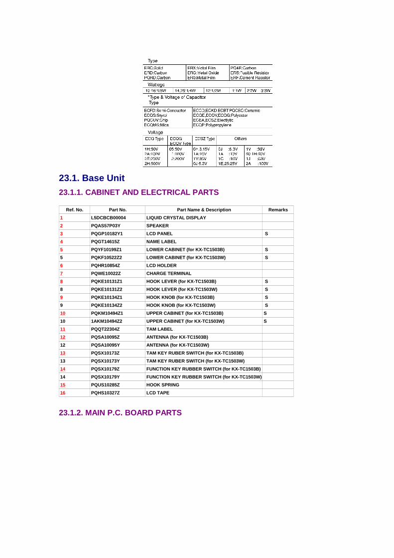
4. RESISTORS & CAPACITORSUnless otherwise specified;All resistors are in ohms ( ) K=1000 , M=1000k All capacitors are in MICRO FARADS ( F) P= F*Type & Wattage of Resistor
23.1. Base Unit23.1.1. CABINET AND ELECTRICAL PARTS
Ref. No. Part No. Part Name & Description Remarks1 L5DCBCB00004 LIQUID CRYSTAL DISPLAY 2 PQAS57P03Y SPEAKER 3 PQGP10182Y1 LCD PANEL S4 PQGT14615Z NAME LABEL5 PQYF10199Z1 LOWER CABINET (for KX-TC1503B) S5 PQKF10522Z2 LOWER CABINET (for KX-TC1503W) S6 PQHR10854Z LCD HOLDER7 PQWE10022Z CHARGE TERMINAL8 PQKE10131Z1 HOOK LEVER (for KX-TC1503B) S8 PQKE10131Z2 HOOK LEVER (for KX-TC1503W) S9 PQKE10134Z1 HOOK KNOB (for KX-TC1503B) S9 PQKE10134Z2 HOOK KNOB (for KX-TC1503W) S10 PQKM10494Z1 UPPER CABINET (for KX-TC1503B) S10 1AKM10494Z2 UPPER CABINET (for KX-TC1503W) S11 PQQT22304Z TAM LABEL12 PQSA10095Z ANTENNA (for KX-TC1503B) 12 PQSA10095Y ANTENNA (for KX-TC1503W) 13 PQSX10173Z TAM KEY RUBER SWITCH (for KX-TC1503B) 13 PQSX10173Y TAM KEY RUBER SWITCH (for KX-TC1503W) 14 PQSX10179Z FUNCTION KEY RUBBER SWITCH (for KX-TC1503B)14 PQSX10179Y FUNCTION KEY RUBBER SWITCH (for KX-TC1503W)15 PQUS10285Z HOOK SPRING16 PQHS10327Z LCD TAPE
23.1.2. MAIN P.C. BOARD PARTS

Ref. No. Part No. Part Name & Description RemarksPCB1 PQWPTC1503BH MAIN P.C.BAORD ASS'Y (RTL)
(ICS)IC100 C0CBABD00013 IC IC201 C2HBBG000011 IC IC300 PQWITC1503BH IC IC331 PQVIPS3432UT IC SIC332 C0EBE0000142 IC
(TRANSISTORS)Q1 2SC2120 TRANSISTOR(SI) SQ3 PQVT2N6517CA TRANSISTOR(SI) SQ4 2SA1625 TRANSISTOR(SI) SQ5 UN5213 TRANSISTOR(SI) SQ6 2SD1819A TRANSISTOR(SI) Q7 2SD1819A TRANSISTOR(SI) Q50 2SD1819A TRANSISTOR(SI) Q102 2SD1819A TRANSISTOR(SI) Q104 2SD1758Q TRANSISTOR(SI) SQ108 2SD2136 TRANSISTOR(SI) Q150 2SD1994A TRANSISTOR(SI) Q151 2SD1819A TRANSISTOR(SI)
(DIODES)D1 PQVDRLZ2R0 DIODE(SI) SD2 PQVDRLZ20A DIODE(SI) SD3 MA111 DIODE(SI) D4 PQVDS1ZB60F1 DIODE(SI) D101 PQVDHRU0302A DIODE(SI) SD102 PQVDHRU0302A DIODE(SI) SD103 MA8039 DIODE(SI) D105 PQVDHRU0302A DIODE(SI) SD106 PQVDHRU0302A DIODE(SI) SD107 MA8068M DIODE(SI) D152 PQVDRLZ20A DIODE(SI) SD153 PQVDRLZ20A DIODE(SI) SD202 MA111 DIODE(SI) D203 MA111 DIODE(SI)
(LEDS)LED202 PQVDSML310MT LED SLED203 PQVDEL1921SR LED
(COILS)L1 PQLQXF330K COIL SL2 PQLQXF330K COIL SL150 PQLQZK3R3K COIL SL151 PQLQXF330K COIL SL200 PQLQR2KA213 COIL SL201 PQLQR4RB601D COIL
(SURGE ABSORBERS)SA1 PQVDDSS301L SURGE ABSORBER SSA2 PQVDDSS301L SURGE ABSORBER S
(OTHERS)CN1 PQJJ2H003Z JACK SOCKET SE1 PQJM147Y MICROPHONEE2 PQMG10023Z CUSHION RUBBER, MICG401 PQJT10152Z CHARGE TERMINALG402 PQJT10152Z CHARGE TERMINAL

Ref. No. Part No. Part Name & Description RemarksG403 PQJT10152Z CHARGE TERMINALG404 PQJT10152Z CHARGE TERMINALG405 PQJT10152Z CHARGE TERMINALG406 PQJT10152Z CHARGE TERMINALPOS1 PQRPAR390N POSISTOR SRA200 EXRV8V104JV RESISTOR ARRAY SX200 H0D409400014 CRYSTAL OSCILLATOR
(RESISTORS)R1 ERJ3GEYJ122 1.2k R2 ERJ3GEYJ681 680R3 ERJ3GEYJ470 47R5 ERDS1TJ330 33 SR7 ERJ3GEYJ393 39k R8 ERJ3GEY0R00 0R10 ERJ3GEYJ102 1k R13 ERJ3GEYJ473 47k R17 ERJ3GEYJ473 47k R18 ERJ3GEYJ103 10k R19 ERJ3GEYJ563 56k R20 ERD25TJ104 100k SR21 ERJ3GEYJ103 10k R23 ERDS1VJ106 10M R24 ERJ3GEYJ275 2.7M R25 ERJ3GEYJ155 1.5M R26 ERJ3GEYJ472 4.7k R29 ERJ3GEYJ472 4.7k R30 ERJ3GEYJ104 100k R31 ERJ3GEYJ104 100k R50 ERJ3GEYJ102 1k R51 ERJ3GEYJ470 47R52 ERJ3GEYJ394 390k R55 ERJ3GEYJ102 1k R57 ERJ3GEY0R00 0R70 ERJ3GEYJ392 3.9k R102 ERJ3GEYJ224 220k R104 ERJ3GEYJ473 47k R105 ERJ3GEYJ103 10k R107 ERJ3GEYJ331 330R109 ERJ3GEYJ683 68k R112 ERJ3GEYJ273 27k R114 ERDS1TJ181 180 SR116 ERJ3GEY0R00 0R117 ERJ3GEY0R00 0R118 ERJ3GEYJ102 1k R150 ERJ3GEYJ104 100k R151 ERJ3GEYJ561 560R152 ERJ3GEYJ331 330R153 ERDS1TJ100 10 SR157 ERDS1TJ391 390 SR159 ERJ3GEYJ103 10k R160 ERJ3GEYJ563 56k R161 ERJ3GEYJ563 56k R200 ERJ3GEYJ101 100R201 ERJ3GEYJ101 100

Ref. No. Part No. Part Name & Description RemarksR203 ERJ3GEYJ473 47k R204 ERJ3GEYJ391 390R206 ERJ3GEYJ181 180R212 ERJ3GEYJ102 1k R213 ERJ3GEYJ102 1k R214 ERJ3GEYJ102 1k R215 ERJ3GEYJ222 2.2k R216 ERJ3GEYJ222 2.2k R219 ERJ3GEYJ103 10k R222 ERJ3GEYJ333 33k R223 ERJ3GEYJ222 2.2k R225 ERJ3GEYJ102 1k R227 ERJ3GEYJ222 2.2k R228 ERJ3GEYJ473 47k R229 ERJ3GEYJ473 47k R230 ERJ3GEY0R00 0R231 ERJ3GEY0R00 0R232 ERJ3GEY0R00 0R233 ERJ3GEY0R00 0R234 ERJ3GEY0R00 0R251 ERJ3GEYJ102 1k R252 ERJ3GEYJ102 1k R300 ERJ3GEYJ104 100k R301 ERJ3GEYJ103 10k R400 ERJ3GEYJ332 3.3k R900 ERJ3GEYJ472 4.7k R901 ERJ3GEYJ472 4.7k R909 ERJ3GEYJ101 100R910 ERJ3GEYJ472 4.7k R911 ERJ3GEYJ472 4.7k R912 ERJ3GEYJ472 4.7k C57 ERJ3GEY0R00 0C61 ERJ3GEY0R00 0J201 ERJ3GEYJ472 0J202 ERJ3GEY0R00 0
(CAPACITORS)C1 ECEA1CKA100 10C3 ECUV1C473KBV 0.047C4 ECUV1H101JCV 100P C6 ECUV1H103KBV 0.01C8 ECEA1HKA010 1C9 ECUV1H103KBV 0.01 SC14 ECUV1H103KBV 0.01C15 PQCUV1A684KB 0.68C16 PQCUV1H154KR 0.15C17 PQCUV1H154KR 0.15C18 ECKD2H681KB 680P SC19 ECKD2H681KB 680P SC50 ECUV1C104KBV 0.1C55 ECUV1H102KBV 0.001 SC58 ECUV1C104KBV 0.1C70 ECEV0JA220 22C100 ECUV1C104ZFV 0.1C101 ECEV0JA101 100

Ref. No. Part No. Part Name & Description RemarksC103 ECEA0JU102 1000C105 PQCUV1C334KB 0.33C106 ECUV1C104ZFV 0.1C107 ECEV0JA220 22C108 ECEV0JA101 100C109 ECUV1H103KBV 0.01 SC110 ECUV1C104ZFV 0.1C112 ECEA1AKA101 100C114 ECEA1CKS220 22 SC150 ECUV1C104ZFV 0.1C200 ECUV1C104ZFV 0.1C201 ECUV1H681JCV 680P SC207 ECUV1C104ZFV 0.1C213 ECUV1C104ZFV 0.1C227 ECUV1H180JCV 18P C228 ECUV1H150JCV 15P C230 ECST0JY106 10C231 ECUV1C104ZFV 0.1C234 ECUV1H103KBV 0.01 SC235 ECUV1H103KBV 0.01C236 ECUV1H103KBV 0.01C237 ECST0JY106 10C238 ECUV1H103KBV 0.01 SC239 ECEA0JU331 330C241 ECUV1C104ZFV 0.1C242 ECUV1H272KBV 0.0027C244 ECUV1C104KBV 0.1C250 ECUV1C104KBV 0.1C251 ECUV1C104ZFV 0.1C252 ECUV1C104ZFV 0.1C300 ECUV1H101JCV 100P C301 ECUV1H101JCV 100P C302 ECUV1H101JCV 100P C303 ECUV1H101JCV 100P C304 ECUV1H101JCV 100P C305 ECUV1H101JCV 100P C306 ECUV1H101JCV 100P C307 ECUV1H101JCV 100P C308 ECUV1C104ZFV 0.1C309 ECUV1C104ZFV 0.1C310 ECUV1H101JCV 100P C311 ECUV1H101JCV 100P C312 ECUV1H101JCV 100P C313 ECUV1H101JCV 100P C315 ECUV1H101JCV 100P C401 ECUV1H103KBV 0.01 SC403 ECUV1H330JCV 33P C404 ECUV1H101JCV 100P C405 ECUV1H101JCV 100P C406 ECUV1H101JCV 100P C407 ECUV1H101JCV 100P C408 ECUV1H101JCV 100P C409 ECUV1H030CCV 3P C410 ECUV1H101JCV 100P
Ref. No. Part No. Part Name & Description RemarksC411 ECUV1H101JCV 100P C412 ECUV1H101JCV 100P C413 ECUV1C104KBV 0.1C415 ECEV0JA220 22C450 ECEV0JA101 100C453 ECUV1H030CCV 3P C723 ECUV1C563KBV 0.056
23.1.3. RF P.C.BOARD PART
Ref. No. Part No. Part Name & Description RemarksPCB2 PQLP10246Z RF BLOCK
23.2. Handset23.2.1. CABINET AND ELECTRICAL PARTS
Ref. No. Part No. Part Name & Description Remarks101 PQAS3P07Y SPEAKER 102 PQAX3P27Z RECEIVER103 PQBC10341Z1 NAVIKEY BUTTON S104 PQSA10102X ANTENNA (KX-TC1503B) S104 PQSA10102W ANTENNA (KX-TC1503W) S105 PQGT14617Z NAME LABEL106 PQHE10121Z CUSHION, URETHANE FORM107 PQHG10589Y SP RUBBER SHEET108 PQHR10778Z SP HOLDER109 PQHR10855Z SP HOLDER110 PQHR10865Z LED LENSE111 PQHS10457Z SP NET112 PQP504SVC BATTERY S113 PQSX10174Y KEY RUBBER SWITCH (KX-TC1503B)113 PQSX10174W KEY RUBBER SWITCH (KX-TC1503W)114 PQJT10176Z CHARGE TERMINAL (L)115 PQJT10177Z CHARGE TERMINAL (R)116 PQKE10132Z1 EARPHONE CAP S117 PQKM10486Y1 FRONT CABINET (KX-TC1503B) S117 1AKM10486Y4 FRONT CABINET (KX-TC1503W) S118 PQKK10120Z1 BATTERY COVER (KX-TC1503B) S118 PQKK10120Z2 BATTERY COVER (KX-TC1503W) S119 PQKF10518Z1 REAR CABINET (KX-TC1503B) S119 PQKF10518Z2 REAR CABINET (KX-TC1503W) S
23.2.2. MAIN P.C. BOARD PARTS

Ref. No. Part No. Part Name & Description RemarksPCB100 PQWPTC1503BR MAIN P.C.BOARD ASS'Y (RTL)
(ICS)IC201 C2HBBG000014 IC IC202 PQWITC1503BR IC IC203 C0CBABD00011 IC IC204 PQVIC62FP33M IC SIC205 PQVIC61CN32N IC S
(TRANSISTORS)Q205 2SD1819A TRANSISTOR(SI) Q206 PQVTDTC143E TRANSISTOR(SI) SQ207 2SD1819A TRANSISTOR(SI) Q211 PQVTDTA143TU TRANSISTOR(SI)
(DIODES)D201 MA2ZD1400 DIODE(SI) D203 MA111 DIODE(SI) D206 PQVDS1ZB60F1 DIODE(SI) D211 MA8100M DIODE(SI) D214 MA111 DIODE(SI) D215 MA2ZD1400 DIODE(SI) D216 MA111 DIODE(SI)
(LEDS)LED208 PQVDSML310MT LED SLED209 PQVDEL1921SR LEDLED210 PQVDSML310MT LED S
(COILS)L201 MQLRE15NJF COIL L203 PQLQR3FL121 COIL SL211 PQLQR4RB601D COIL L212 PQLQR4RB601D COIL
(CONNECTORS)CN202 PQJP2D13Z CONNECTOR PIN SCN203 PQJJ1J007Z EAR JACK S
(OTHERS)E101 PQJM147Y MICROPHONE G1 PQJT10152Z CHARGE TERMINALG2 PQJT10152Z CHARGE TERMINALG3 PQJT10152Z CHARGE TERMINALG4 PQJT10152Z CHARGE TERMINALG5 PQJT10152Z CHARGE TERMINALG6 PQJT10152Z CHARGE TERMINALX201 H0J409400006 CRYSTAL OSCILLATOR
(RESISTORS)R209 ERJ3GEYJ102 1k R210 ERJ3GEYJ103 10k R211 ERJ3GEYJ103 10k R212 ERJ3GEYJ101 100R213 ERJ3GEYJ101 100R214 ERJ3GEYJ331 330R215 ERJ3GEYJ681 680R216 ERJ3GEYJ331 330R222 ERJ3GEYJ101 100R224 ERJ3GEYJ103 10k R225 ERJ3GEYJ472 4.7k R228 ERJ3GEYJ224 220k

Ref. No. Part No. Part Name & Description RemarksR229 ERJ3GEYJ102 1k R230 ERJ3GEYJ102 1k R231 ERJ3GEYJ102 1k R232 ERJ3GEYJ103 10k R233 ERJ3GEY0R00 0R234 ERJ3GEYJ225 2.2M R235 ERJ3GEYJ225 2.2M R236 ERJ3GEYJ473 47k R241 ERJ3GEY0R00 0R244 ERJ3GEYJ473 47k R245 ERJ3GEYJ103 10k R246 ERJ3GEYJ153 15k R247 ERJ3GEYJ391 390R248 ERJ3GEYJ393 39k R249 ERJ3GEYJ222 2.2k R250 ERJ3GEYJ222 2.2k R253 ERJ3GEYJ222 2.2k R260 ERJ3GEYJ103 10k R265 ERJ3GEYJ103 10k R270 ERJ3GEYJ104 100k R271 ERJ3GEYJ104 100k R272 ERJ3GEYJ104 100k R300 ERJ3GEYJ104 100k R302 ERJ3GEYJ180 18R303 ERJ3GEYJ180 18C301 ERJ3GEY0R00 0L209 PQ4R10XJ000 0 S
(CAPACITORS)C203 ECUV1C104ZFV 0.1C205 ECUV1H101JCV 100P C213 ECEV0JA101 100C214 ECUV1C104ZFV 0.1C217 ECUV1C104ZFV 0.1C218 ECUV1C104ZFV 0.1C220 ECEV0JA101 100C221 ECUV1C104ZFV 0.1C222 ECUV1C104ZFV 0.1C223 ECST0JY106 10C224 ECUV1C104ZFV 0.1C225 ECUV1C104ZFV 0.1C226 ECUV1C104ZFV 0.1C227 ECUV1C104ZFV 0.1C228 ECUV1C104ZFV 0.1C229 ECUV1A105ZFV 1C230 ECUV1E333KBV 0.033C231 ECUV1A224KBV 0.22C232 ECUV1E333KBV 0.033C233 ECUV1A105ZFV 1C234 ECUV1A224KBV 0.22C236 ECUV1H150JCV 15P C237 ECUV1H150JCV 15P C239 ECUV1C104ZFV 0.1C242 ECUV1C104ZFV 0.1C255 ECUV1A224KBV 0.22
Ref. No. Part No. Part Name & Description RemarksC257 ECST0JY226 22C262 ECUV1A105ZFV 1C267 ECST0JX226 22C270 ECST0JY475 4.7C274 ECUV1C104ZFV 0.1C277 ECUV1C563KBV 0.056C279 ECUV1H010CCV 1P C280 ECUV1C104ZFV 0.1C282 ECUV1C104ZFV 0.1C285 ECUV1C105ZF 1C291 ECUV1C104ZFV 0.1C294 ECUV1C104ZFV 0.1C303 ECST0JY106 10C304 ECUV1C104ZFV 0.1C305 ECUV1H030CCV 3P
23.2.3. RF P.C.BOARD PART
Ref. No. Part No. Part Name & Description RemarksPCB200 PQLP10246Z RF BLOCK
23.2.4. ACCESSORIES AND PACKING MATERIALS
Ref. No. Part No. Part Name & Description RemarksA1 KX-TCA1-G AC ADAPTOR A2 PQJA10075Z TEL CORDA3 PQKE10130Z1 BELT CLIP (KX-TC1503B) SA3 PQKE10130Z2 BELT CLIP (KX-TC1503W) SA4 PQKL10035Z1 WALL MOUNT ADAPTOR (KX-TC1503B) SA4 PQKL10035Z2 WALL MOUNT ADAPTOR (KX-TC1503W) SA5 PQQW12431Z QUICK GUIDE (for English)A6 PQQW12432Z QUICK GUIDE (for Spanish)A7 PQQX13049Z INSTRUCTION BOOK P1 PQPP170Y PROTECTION COVER (for Base Unit)P2 XZB10X35A02 PROTECTION COVER (for Handset)P3 PQPK13410Z CARTON BOX (KX-TC1503B)P3 PQPK13473Z CARTON BOX (KX-TC1503W)P4 PQPD10469Z CUSHION P5 PQXDDS400-8 SECURITY TAGP6 PQXDZLDRS1 SECURITY TAG
24. FOR SCHEMATIC DIAGRAM24.1. Base Unit (SCHEMATIC DIAGRAM (Base Unit))Notes:
1. DC voltage measurements are taken with voltmeter from the negative voltage line.
2. The schematic diagrams and circuit board may be modified at any time with the development of new technology.
24.2. Handset (SCHEMATIC DIAGRAM (Handset))Notes:
1. DC voltage measurements are taken with an oscilloscope or a tester with a ground.
2. The schematic diagrams and circuit board may be modified at any time with the development of new technology.
24.3. Memo
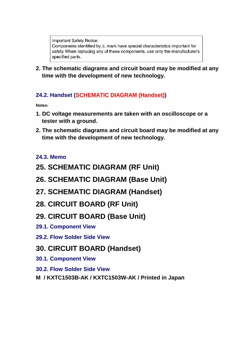
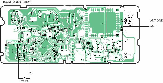
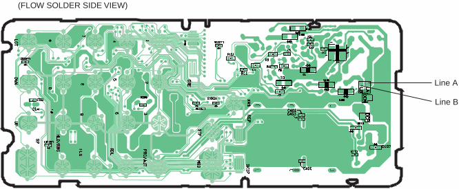
25. SCHEMATIC DIAGRAM (RF Unit)26. SCHEMATIC DIAGRAM (Base Unit)27. SCHEMATIC DIAGRAM (Handset)28. CIRCUIT BOARD (RF Unit)29. CIRCUIT BOARD (Base Unit)29.1. Component View
29.2. Flow Solder Side View
30. CIRCUIT BOARD (Handset)30.1. Component View
30.2. Flow Solder Side ViewM / KXTC1503B-AK / KXTC1503W-AK / Printed in Japan
IC300
IC202
IC331
IC332
IC100
IC201
ANT GND
ANT
(COMPONENT VIEW)
TEST
Line A
Line B
(FLOW SOLDER SIDE VIEW)
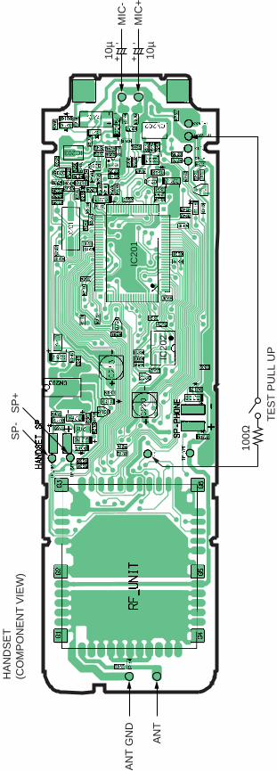
100Ω
AN
T G
ND
HA
ND
SE
T(C
OM
PO
NE
NT
VIE
W)
AN
T
TE
ST
PU
LL U
P
SP
-S
P+
MIC
-
MIC
+10
µ
10µ
+
-
+
-
IC203
IC20
1
IC20
2
IC204
IC205
Q150
Q104
IC332
IC100
IC331
Q151
Q50
Q7 D4Q1
Q4
Q6
Q1083.6V
3.2V
IC201
MIP
HSMIPLOUTO
MIN
IC300
CO
M1~
2S
EG
3~12 LIN
O
VMOD
MODEN
OSCIN (BMCCLK)
CLK
DATA
LE
RXEN
TXEN
RADIO EN
SHCTRL
RSSI
RXDATA (RXI)
Key Scan
LCD CON
LCDKey matrex
TX
RX
16 2
15
14
13
12
11
10
9
8
7
6
5
4
IC101
IC102

15P
(1)
(2)(
3)(4
)(1
3)(1
4)(1
5)(1
6)(1
7~19
)(2
0)(2
1)(2
2)(2
6)(2
3~25
)(5
~12
)IC201
IC202NC
IC300
TALK TX
TALK RX
3.2V
6.0V3.3V 3.6V
9V DC.
KX-TC1503B/W: SCHEMATIC DIAGRAM (Base Unit)
Output
Input 1.1kHz140mVp-p (-25dBm/600 )
2.7M
IC331
IC100
IC332
(1)
(2)(
3)(4
)(1
3)(1
4)(1
5)(1
6)(1
7~19
)(2
0)(2
1)(2
2)(2
6)(2
3~25
)(5
~12
)
for H/S

TALK TX
TALK RX
3.2V
6.0V3.3V 3.6V
9V DC.
KX-TC1503B/W: SCHEMATIC DIAGRAM (Base Unit)
Output
Input 1.1kHz140mVp-p (-25dBm/600 )
2.7M
IC331
IC100
IC332
(1)
(2)(
3)(4
)(1
3)(1
4)(1
5)(1
6)(1
7~19
)(2
0)(2
1)(2
2)(2
6)(2
3~25
)(5
~12
)
for H/S
IC202
(1)(
2)(3
)(4
~12
)(1
3~15
)(1
7~29
)(3
0~34
)(3
5~37
)(38
~40
)(4
2~48
)(4
1)(1
6)

TX
RX
6.3V/22µ
IC203
IC205
IC201
IC204
3.3V
3.3V
(Headset)
(Headset)Input 1.1kHz-43dBm/600
Input 1.1kHz18mVp-p (-45dBm/600 )
(1)(
2)(3
)(4
~12
)(1
3~15
)(1
7~29
)(3
0~34
)(3
5~37
)(38
~40
)(4
2~48
)(4
1)(1
6)
KX-TC1503B/W : SCHEMATIC DIAGRAM (Handset)
TX
RX
6.3V/22µ
IC203
IC205
IC201
IC204
3.3V
3.3V
(Headset)
(Headset)Input 1.1kHz-43dBm/600
Input 1.1kHz18mVp-p (-45dBm/600 )
(1)(
2)(3
)(4
~12
)(1
3~15
)(1
7~29
)(3
0~34
)(3
5~37
)(38
~40
)(4
2~48
)(4
1)(1
6)
KX-TC1503B/W : SCHEMATIC DIAGRAM (Handset)
IC101IC
102
IC30
0
IC20
2
IC33
1
IC33
2
IC10
0
IC201
X200
UA
RT
_RX
UA
RT
_TX
1
30
50
31
51
80
81
100
1
2223
44
1
G
2 3 4 5
6
7
8
9
10
11
12
13
GG
1516 14G G
G
G
G
18
17
G
TP
_SY
NC
WIN
TP
_SY
ND
ET
VRF LINO Min
Mic input
Mip X'tal CLK Reset: RST Power-Down: PDN
Vcc (3.3V)B
CHARGE-CTLHS MIPVcc (3.3V) Louto BellB
Vcc (3.2V)D
IC20
3
IC201
IC202
IC20
4
IC20
5
1
G
2 3 4 5
6
7
8
9
10
11
12
13
GG
1516 14G G
G
G
G
18
17
G
MIC
MM
ICP
1100
3031
50
518081
1 CHANGES 2
1.1. REPLACEMENT PARTS LIST 2
© 2007 Panasonic Communications Co., Ltd. Allrights reserved. Unauthorized copying anddistribution is a violation of law.
KX-TC1503BKX-TC1503W900MHz Digital Cordless AnsweringSystemBlack Version
White Version
(for U.S.A.)
(for Panama)
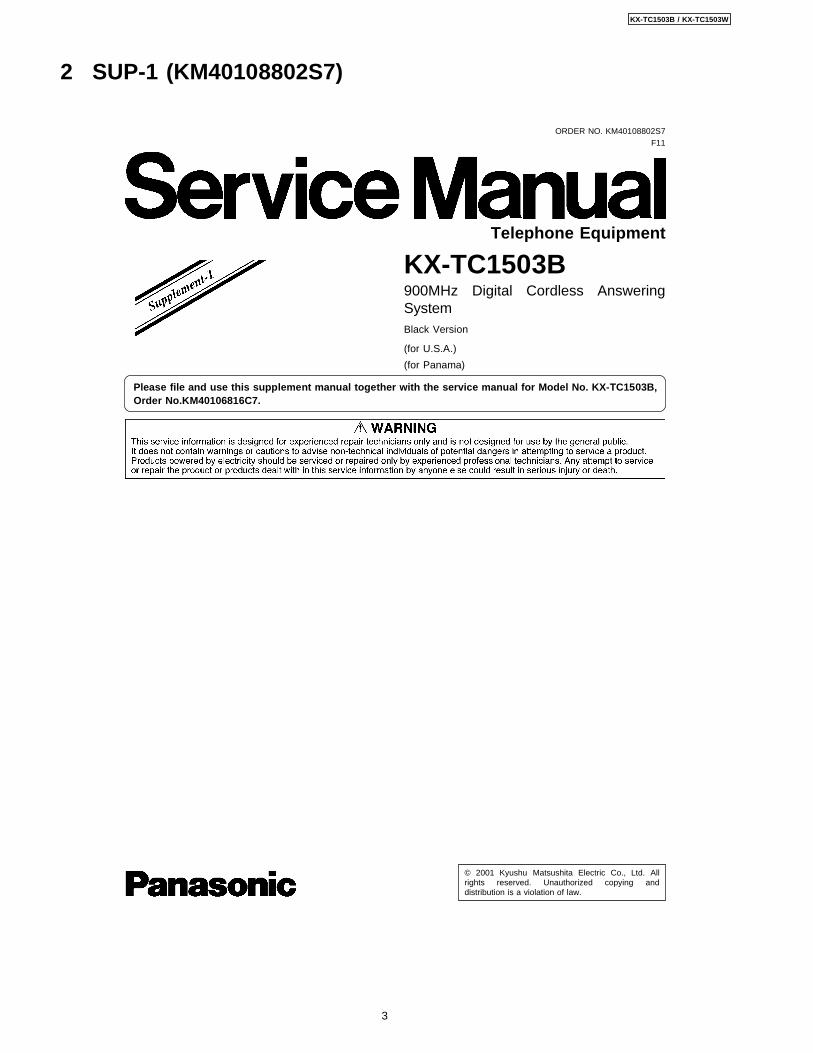
2 SUP-1 (KM40108802S7) 3
Telephone Equipment
Please file and use this supplement manual together with the service manual mentioned below.
CONTENTS Page Page
ORDER NO. KM40701642SEF11
1 CHANGES
1.1. REPLACEMENT PARTS LIST
1.1.1. REFERENCE CHART
1.1.2. ORIGINAL AND NEW PARTS COMPARISON LISTS
(for KX-TC1503B/KX-TC1503W)
Ref. No. Part No. Part Name & Description Pcs/Set
Remarks Notes Time of ChangeOriginal (Old) New (Suffix)
A1 KX-TCA1-G KX-TCA1-3 AC Adaptor 1 a 4 W -
2
KX-TC1503B / KX-TC1503W
2 SUP-1 (KM40108802S7)
© 2001 Kyushu Matsushita Electric Co., Ltd. Allrights reserved. Unauthorized copying anddistribution is a violation of law.
KX-TC1503B900MHz Digital Cordless AnsweringSystemBlack Version
(for U.S.A.)
(for Panama)
Telephone Equipment
Please file and use this supplement manual together with the service manual for Model No. KX-TC1503B,Order No.KM40106816C7.
ORDER NO. KM40108802S7F11
3
KX-TC1503B / KX-TC1503W
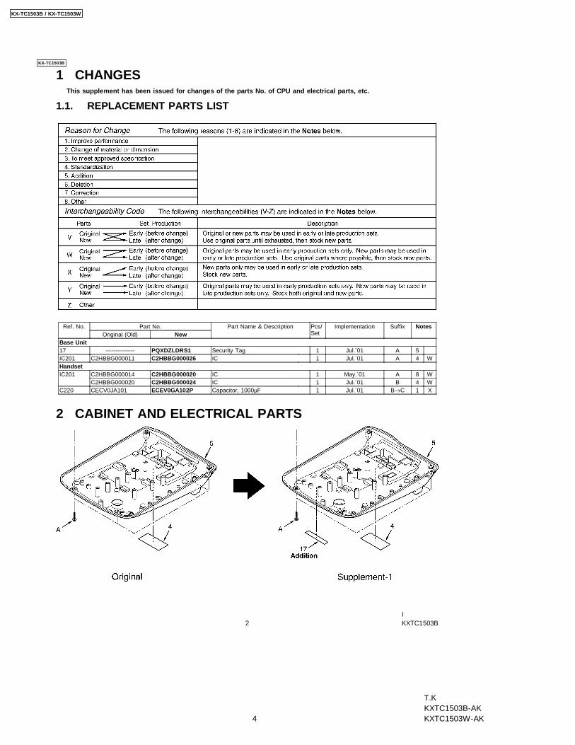
1 CHANGESThis supplement has been issued for changes of the parts No. of CPU and electrical parts, etc.
1.1. REPLACEMENT PARTS LIST
Ref. No. Part No. Part Name & Description Pcs/Set
Implementation Suffix NotesOriginal (Old) New
Base Unit17 --------------- PQXDZLDRS1 Security Tag 1 Jul.´01 A 5IC201 C2HBBG000011 C2HBBG000026 IC 1 Jul.´01 A 4 WHandsetIC201 C2HBBG000014 C2HBBG000020 IC 1 May.´01 A 8 W
C2HBBG000020 C2HBBG000024 IC 1 Jul.´01 B 4 WC220 CECV0JA101 ECEV0GA102P Capacitor, 1000µF 1 Jul.´01 B→C 1 X
2 CABINET AND ELECTRICAL PARTS
2
KX-TC1503B
IKXTC1503B
4
KX-TC1503B / KX-TC1503W
T.KKXTC1503B-AKKXTC1503W-AK