Embed Size (px)
Citation preview
lecture: Optical Modulators in Silicon Photonic Circuits
Prepared by Delphine MARRIS-MORINI, Laurent VIVIEN, Gilles RASIGADE
Institut d’Electronique FondamentaleUniversité Paris Sud – FRANCE
Oct 2009
2Silicon Photonics –PhD course prepared within FP7-224312 Helios project
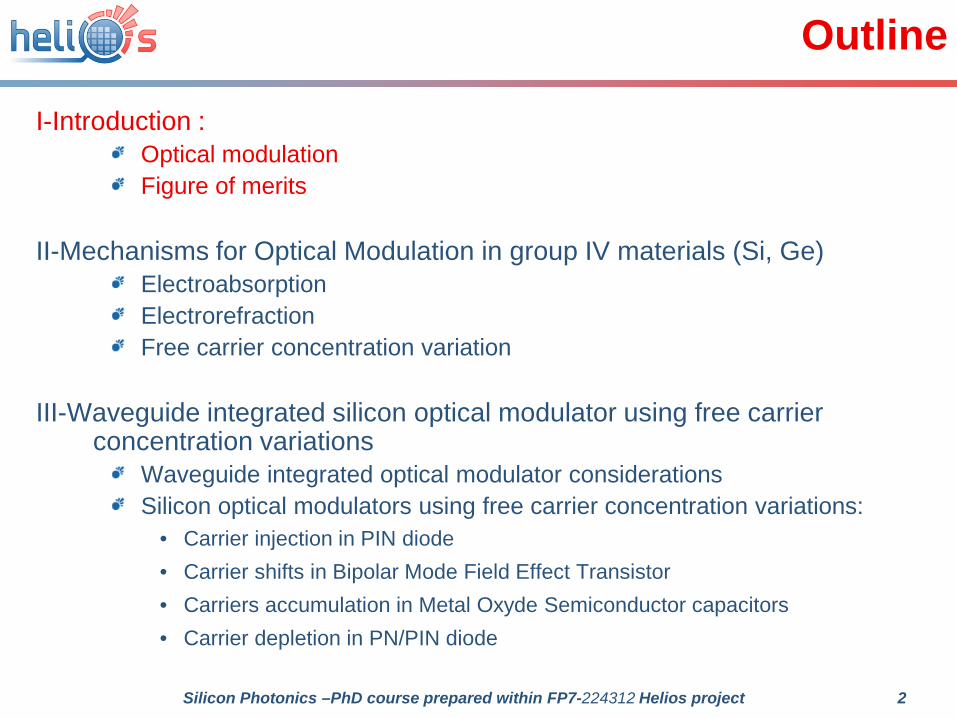
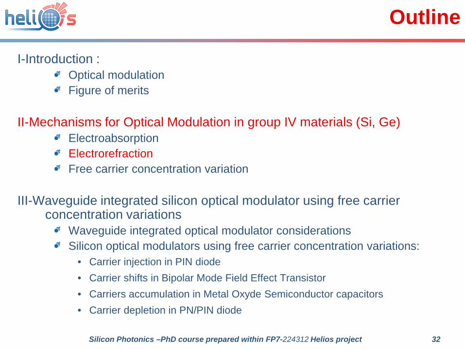
Outline
I-Introduction :Optical modulationFigure of merits
II-Mechanisms for Optical Modulation in group IV materials (Si, Ge)ElectroabsorptionElectrorefractionFree carrier concentration variation
III-Waveguide integrated silicon optical modulator using free carrier concentration variations
Waveguide integrated optical modulator considerationsSilicon optical modulators using free carrier concentration variations:
• Carrier injection in PIN diode• Carrier shifts in Bipolar Mode Field Effect Transistor• Carriers accumulation in Metal Oxyde Semiconductor capacitors• Carrier depletion in PN/PIN diode
3Silicon Photonics –PhD course prepared within FP7-224312 Helios project
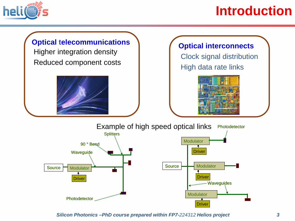
Introduction
Optical telecommunicationsHigher integration densityReduced component costs
Optical interconnects Clock signal distributionHigh data rate links
Photodetector
Source
Splitters
90 ° Bend
Waveguide
Driver
Modulator
Photodetector
Source
Splitters
90 ° Bend
Waveguide
Driver
Modulator
Photodetector
Source
Waveguides
Modulator
Driver
Modulator
Driver
Modulator
Driver
Photodetector
Source
Waveguides
Modulator
Driver
Modulator
Driver
Modulator
Driver
Example of high speed optical links
4Silicon Photonics –PhD course prepared within FP7-224312 Helios project
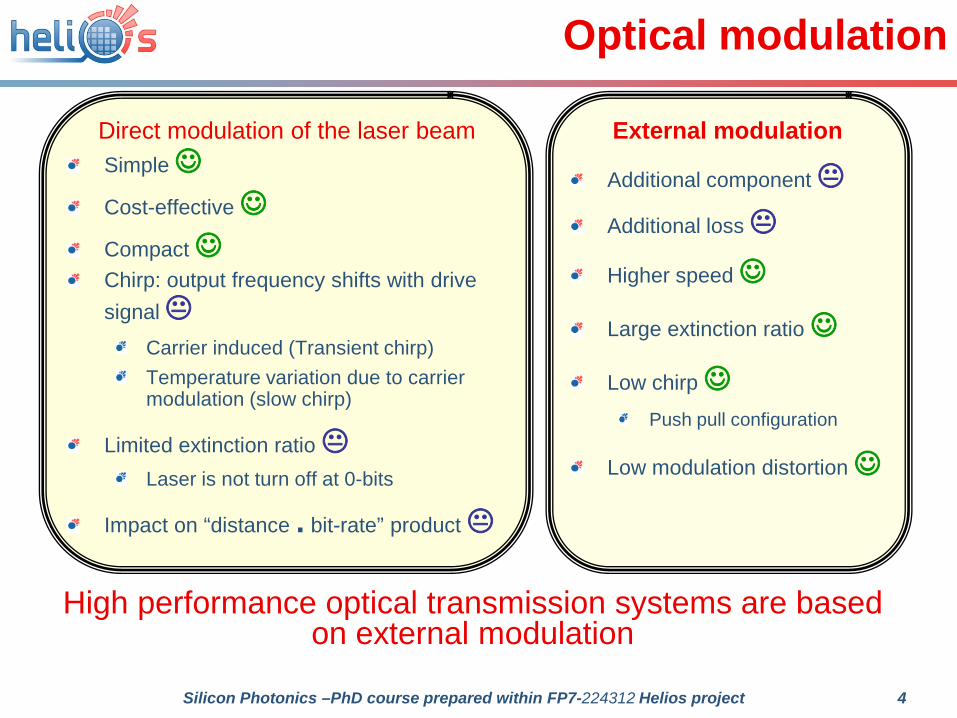
Optical modulation
Simple Cost-effective Compact Chirp: output frequency shifts with drive signal
Carrier induced (Transient chirp) Temperature variation due to carrier modulation (slow chirp)
Limited extinction ratio Laser is not turn off at 0-bits
Impact on “distance . bit-rate” product
Additional component
Additional loss
Higher speed
Large extinction ratio
Low chirp Push pull configuration
Low modulation distortion
Direct modulation of the laser beam External modulation
High performance optical transmission systems are based on external modulation
5Silicon Photonics –PhD course prepared within FP7-224312 Helios project
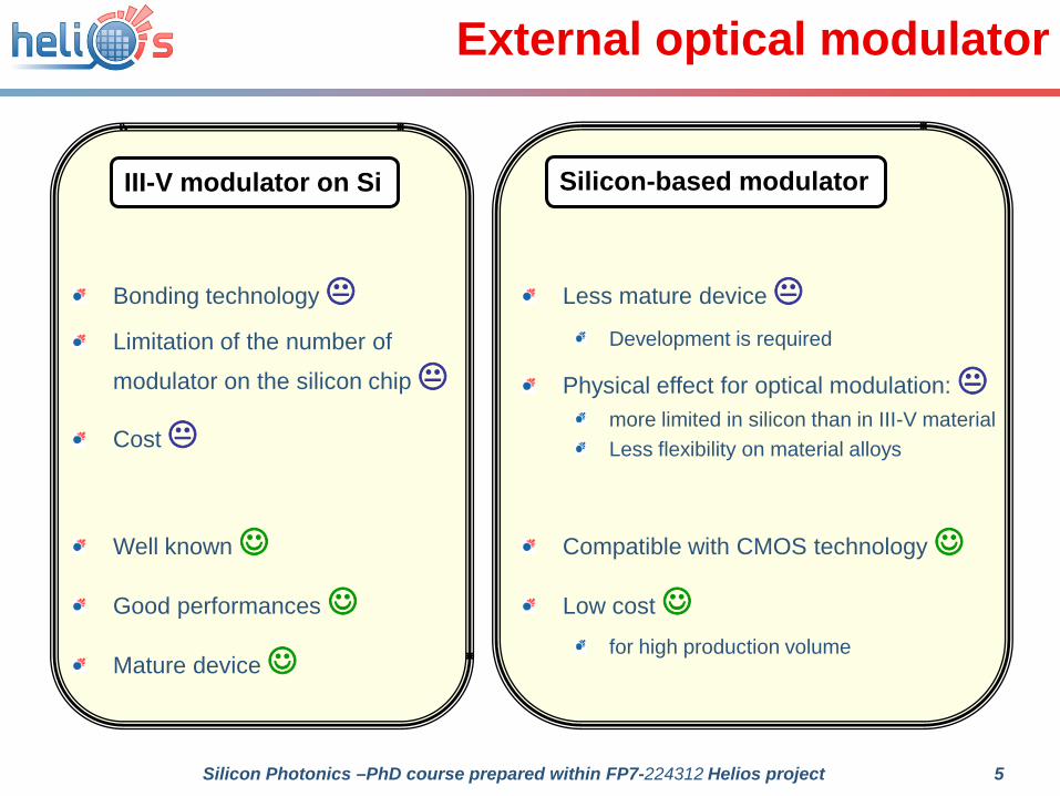
External optical modulator
Bonding technology Limitation of the number of
modulator on the silicon chip
Cost
Well known
Good performances
Mature device
III-V modulator on Si
Less mature device Development is required
Physical effect for optical modulation: more limited in silicon than in III-V materialLess flexibility on material alloys
Compatible with CMOS technology
Low cost for high production volume
Silicon-based modulator
6Silicon Photonics –PhD course prepared within FP7-224312 Helios project
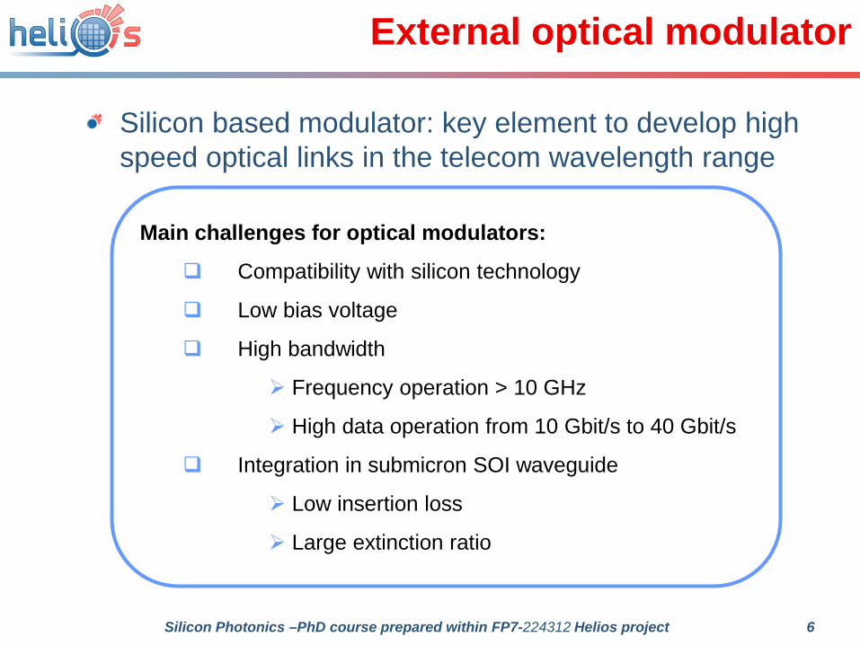
External optical modulator
Silicon based modulator: key element to develop high speed optical links in the telecom wavelength range
Main challenges for optical modulators:
Compatibility with silicon technology
Low bias voltage
High bandwidth
Frequency operation > 10 GHz
High data operation from 10 Gbit/s to 40 Gbit/s
Integration in submicron SOI waveguide
Low insertion loss
Large extinction ratio
7Silicon Photonics –PhD course prepared within FP7-224312 Helios project
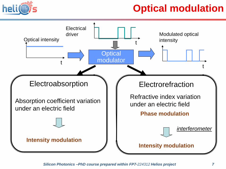
Optical modulation
Opticalmodulatort
Optical intensity
Electrical driver
t
Modulated optical intensityt
Electroabsorption
Phase modulation
Intensity modulation
interferometer
Intensity modulation
Electrorefraction
Absorption coefficient variation under an electric field
Refractive index variation under an electric field
8Silicon Photonics –PhD course prepared within FP7-224312 Helios project
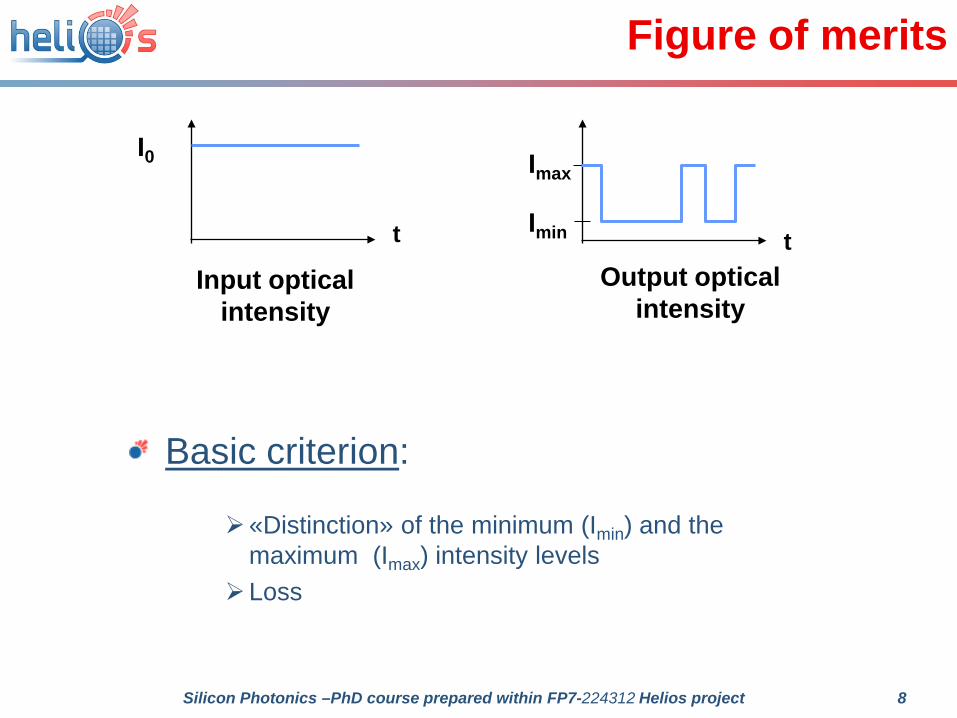
Figure of merits
Basic criterion:
«Distinction» of the minimum (Imin) and the maximum (Imax) intensity levels
Loss
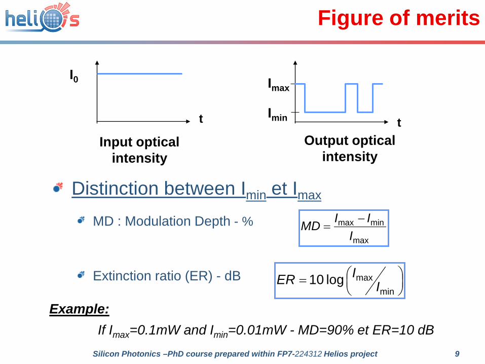
Output optical intensity
tImin
Imax
Input optical intensity
t
I0
9Silicon Photonics –PhD course prepared within FP7-224312 Helios project
Figure of merits
Distinction between Imin et Imax
MD : Modulation Depth - %
Extinction ratio (ER) - dB
max
minmax
IIIMD −
=
Example: If Imax=0.1mW and Imin=0.01mW - MD=90% et ER=10 dB
=
minmaxlog10 I
IER
Output optical intensity
tImin
Imax
Input optical intensity
t
I0
10Silicon Photonics –PhD course prepared within FP7-224312 Helios project
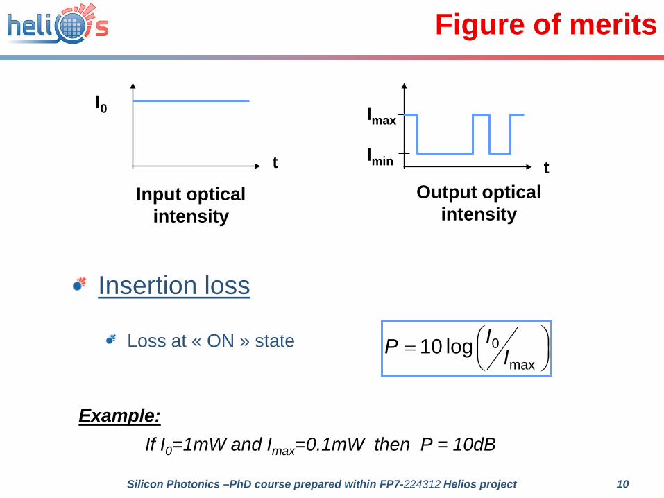
Figure of merits
Insertion loss
Loss at « ON » state
Example: If I0=1mW and Imax=0.1mW then P = 10dB
=
max0log10 I
IP
Output optical intensity
tImin
Imax
Input optical intensity
t
I0
11Silicon Photonics –PhD course prepared within FP7-224312 Helios project
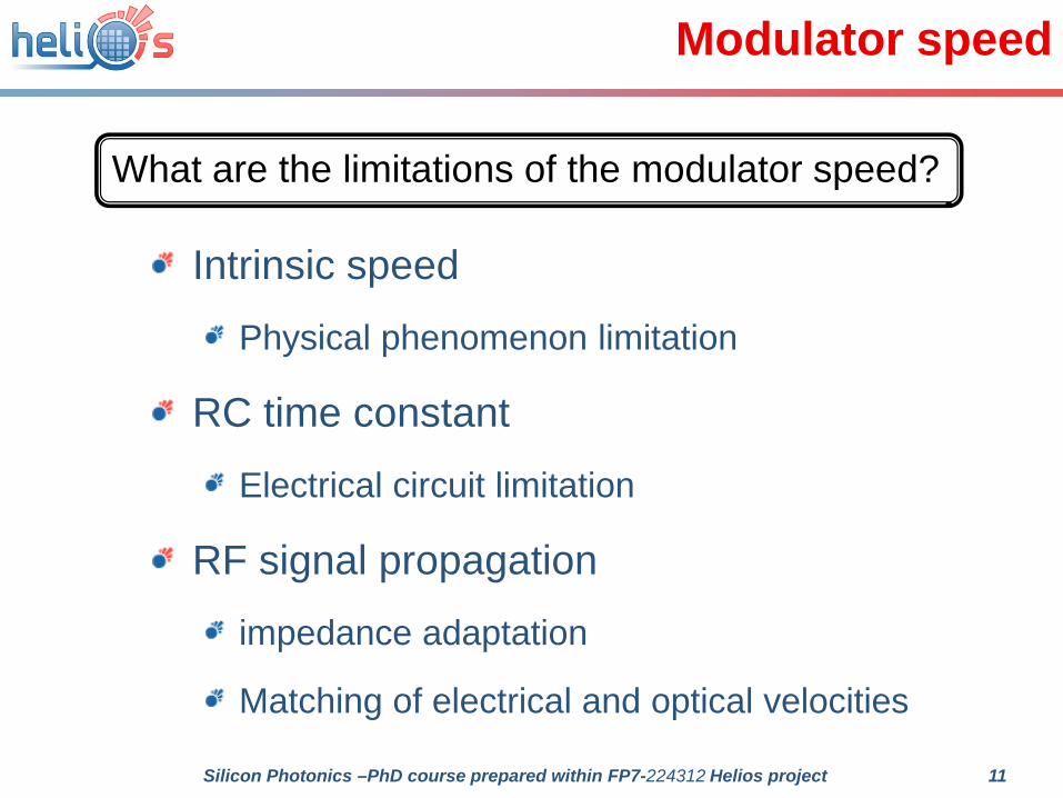
Modulator speed
Intrinsic speed
Physical phenomenon limitation
RC time constant
Electrical circuit limitation
RF signal propagation
impedance adaptation
Matching of electrical and optical velocities
What are the limitations of the modulator speed?
12Silicon Photonics –PhD course prepared within FP7-224312 Helios project
Modulator speed
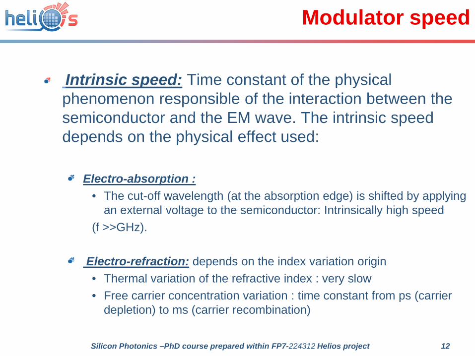
Intrinsic speed: Time constant of the physical phenomenon responsible of the interaction between the semiconductor and the EM wave. The intrinsic speed depends on the physical effect used:
Electro-absorption :• The cut-off wavelength (at the absorption edge) is shifted by applying
an external voltage to the semiconductor: Intrinsically high speed (f >>GHz).
Electro-refraction: depends on the index variation origin• Thermal variation of the refractive index : very slow• Free carrier concentration variation : time constant from ps (carrier
depletion) to ms (carrier recombination)
13Silicon Photonics –PhD course prepared within FP7-224312 Helios project
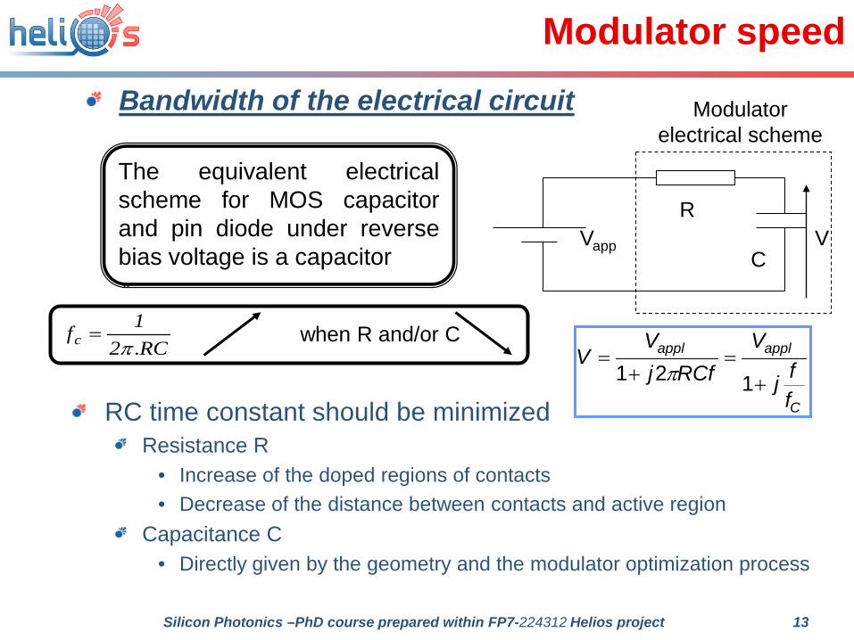
Modulator speed
Bandwidth of the electrical circuit
C
applappl
ffj
VRCfj
VV
+=
+=
121 π
R
CVVapp
RC time constant should be minimizedResistance R
• Increase of the doped regions of contacts• Decrease of the distance between contacts and active region
Capacitance C• Directly given by the geometry and the modulator optimization process
The equivalent electricalscheme for MOS capacitorand pin diode under reversebias voltage is a capacitor
RC21fc .π
= when R and/or C
Modulator electrical scheme
14Silicon Photonics –PhD course prepared within FP7-224312 Helios project
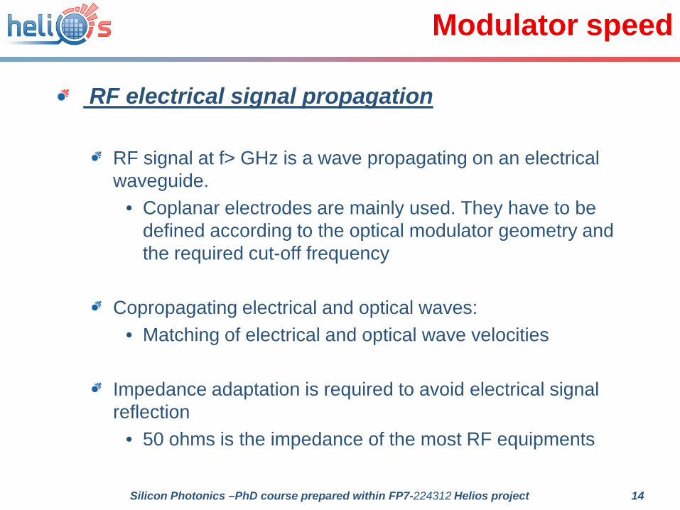
Modulator speed
RF electrical signal propagation
RF signal at f> GHz is a wave propagating on an electrical waveguide.
• Coplanar electrodes are mainly used. They have to be defined according to the optical modulator geometry and the required cut-off frequency
Copropagating electrical and optical waves:• Matching of electrical and optical wave velocities
Impedance adaptation is required to avoid electrical signal reflection
• 50 ohms is the impedance of the most RF equipments

15Silicon Photonics –PhD course prepared within FP7-224312 Helios project
Outline
I-Introduction :Optical modulationFigure of merits
II-Mechanisms for Optical Modulation in group IV materials (Si, Ge)ElectroabsorptionElectrorefractionFree carrier concentration variation
III-Waveguide integrated silicon optical modulator using free carrier concentration variations
Waveguide integrated optical modulator considerationsSilicon optical modulators using free carrier concentration variations:
• Carrier injection in PIN diode• Carrier shifts in Bipolar Mode Field Effect Transistor• Carriers accumulation in Metal Oxyde Semiconductor capacitors• Carrier depletion in PN/PIN diode

16Silicon Photonics –PhD course prepared within FP7-224312 Helios project
Absorption in direct bandgap SC
Interaction between semiconductor (SC) and optical waveBy applying an electrical command, the material should be absorbant or transparent.Photon absorption in SC :
Energy conservationWavevector conservation
α
λ
λG
EG=hc/λG
If hc/λ < EG Transparent If hc/λ > EG absorbantConduction band
Valence band
EG
Electron energy
k = wavevector
Photon energy=hc/λ
Direct bandgap semiconductor
17Silicon Photonics –PhD course prepared within FP7-224312 Helios project
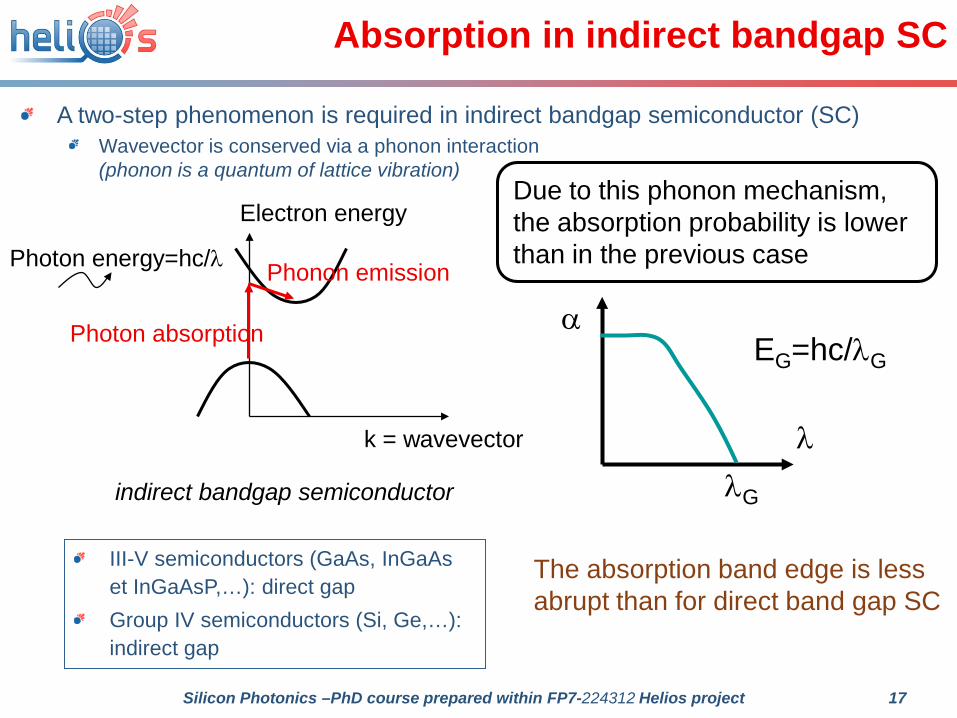
Absorption in indirect bandgap SC
Electron energy
k = wavevector
Photon energy=hc/λ
indirect bandgap semiconductor
A two-step phenomenon is required in indirect bandgap semiconductor (SC)Wavevector is conserved via a phonon interaction (phonon is a quantum of lattice vibration)
Photon absorption
Phonon emission
Due to this phonon mechanism, the absorption probability is lower than in the previous case
EG=hc/λG
α
λλG
The absorption band edge is less abrupt than for direct band gap SC
III-V semiconductors (GaAs, InGaAs et InGaAsP,…): direct gap Group IV semiconductors (Si, Ge,…): indirect gap
18Silicon Photonics –PhD course prepared within FP7-224312 Helios project
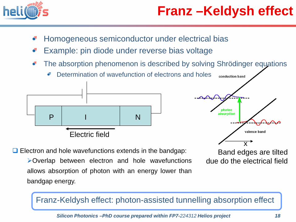
Franz –Keldysh effect
The absorption phenomenon is described by solving Shrödinger equationsDetermination of wavefunction of electrons and holes
Homogeneous semiconductor under electrical biasExample: pin diode under reverse bias voltage
P NI
Electron and hole wavefunctions extends in the bandgap:Overlap between electron and hole wavefunctionsallows absorption of photon with an energy lower thanbandgap energy.
Franz-Keldysh effect: photon-assisted tunnelling absorption effect
Electric field
Band edges are tilted due do the electrical field
x
19Silicon Photonics –PhD course prepared within FP7-224312 Helios project
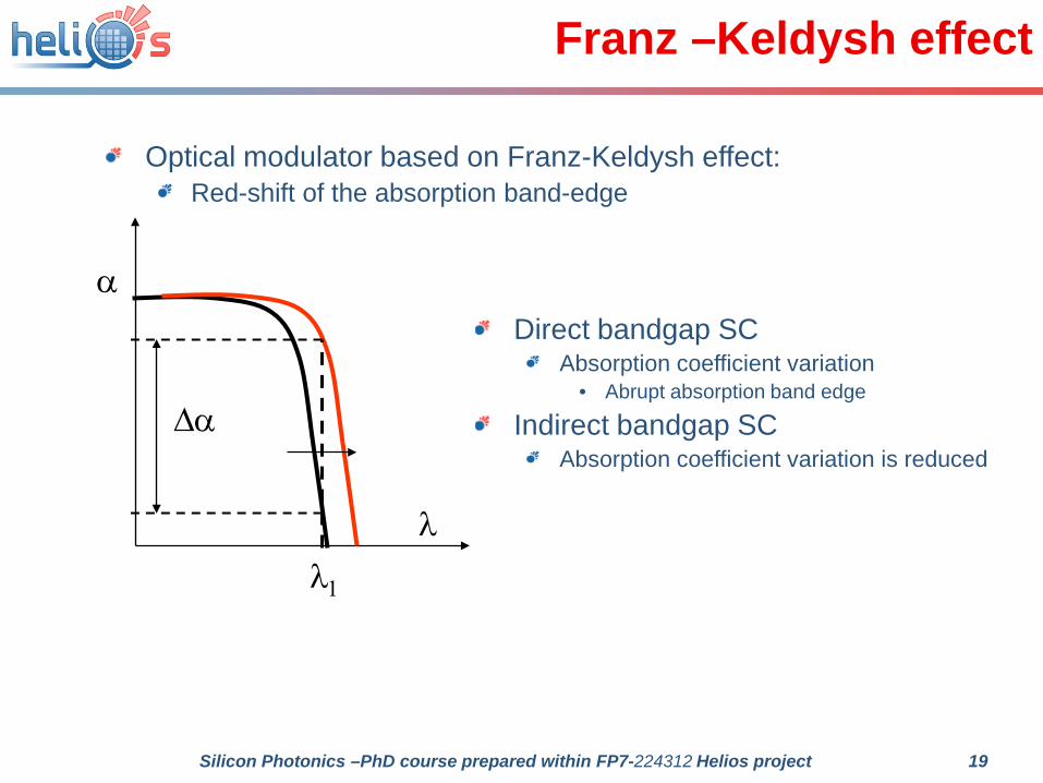
Optical modulator based on Franz-Keldysh effect:Red-shift of the absorption band-edge
Direct bandgap SCAbsorption coefficient variation
• Abrupt absorption band edge
Indirect bandgap SCAbsorption coefficient variation is reduced
Franz –Keldysh effect
α
λ
∆α
λ1
20Silicon Photonics –PhD course prepared within FP7-224312 Helios project
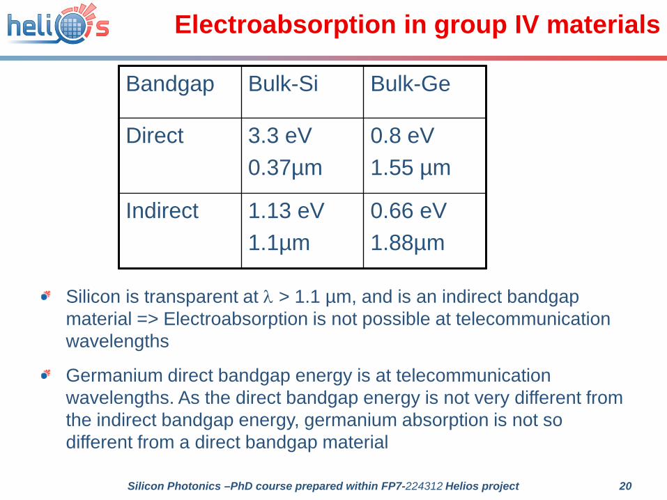
Electroabsorption in group IV materials
Bandgap Bulk-Si Bulk-Ge
Direct 3.3 eV0.37µm
0.8 eV1.55 µm
Indirect 1.13 eV1.1µm
0.66 eV1.88µm
Silicon is transparent at λ > 1.1 µm, and is an indirect bandgap material => Electroabsorption is not possible at telecommunication wavelengths
Germanium direct bandgap energy is at telecommunication wavelengths. As the direct bandgap energy is not very different from the indirect bandgap energy, germanium absorption is not so different from a direct bandgap material
21Silicon Photonics –PhD course prepared within FP7-224312 Helios project
Franz-Keldysh effect
Liu et al., Nature Photonics 2, 433 - 437 (2008)Liu et al., Opt. Express 15, 623 (2007)
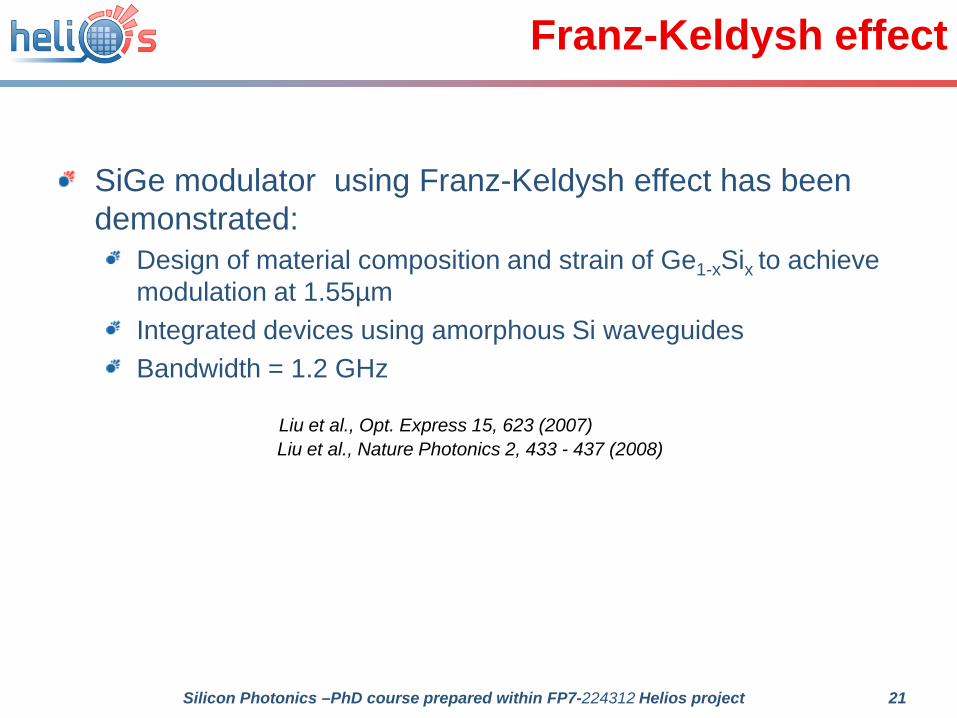
SiGe modulator using Franz-Keldysh effect has been demonstrated:
Design of material composition and strain of Ge1-xSix to achieve modulation at 1.55µmIntegrated devices using amorphous Si waveguidesBandwidth = 1.2 GHz
22Silicon Photonics –PhD course prepared within FP7-224312 Helios project
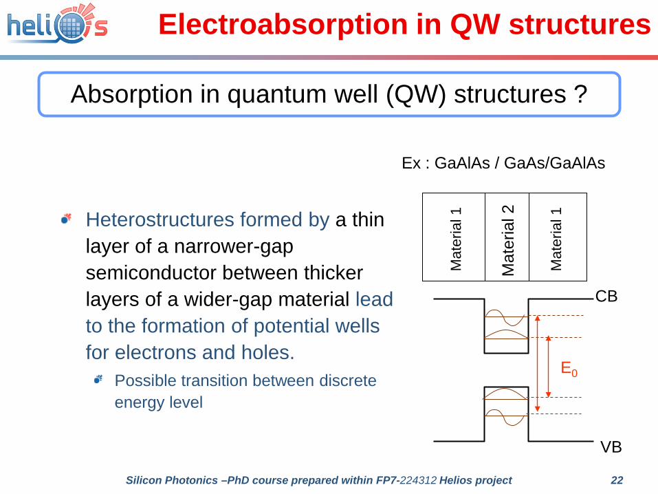
Heterostructures formed by a thin layer of a narrower-gap semiconductor between thicker layers of a wider-gap material lead to the formation of potential wells for electrons and holes.
Possible transition between discrete energy level
E0
CB
VB
Ex : GaAlAs / GaAs/GaAlAs
Electroabsorption in QW structures
Mat
eria
l 1
Mat
eria
l 2
Mat
eria
l 1
Absorption in quantum well (QW) structures ?
23Silicon Photonics –PhD course prepared within FP7-224312 Helios project
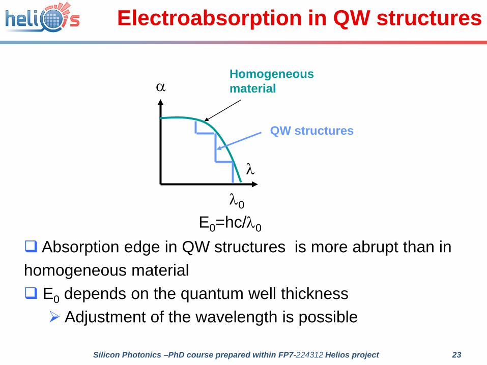
E0=hc/λ0
α
λ
Homogeneous material
QW structures
λ0
Electroabsorption in QW structures
Absorption edge in QW structures is more abrupt than in homogeneous material E0 depends on the quantum well thickness Adjustment of the wavelength is possible
24Silicon Photonics –PhD course prepared within FP7-224312 Helios project
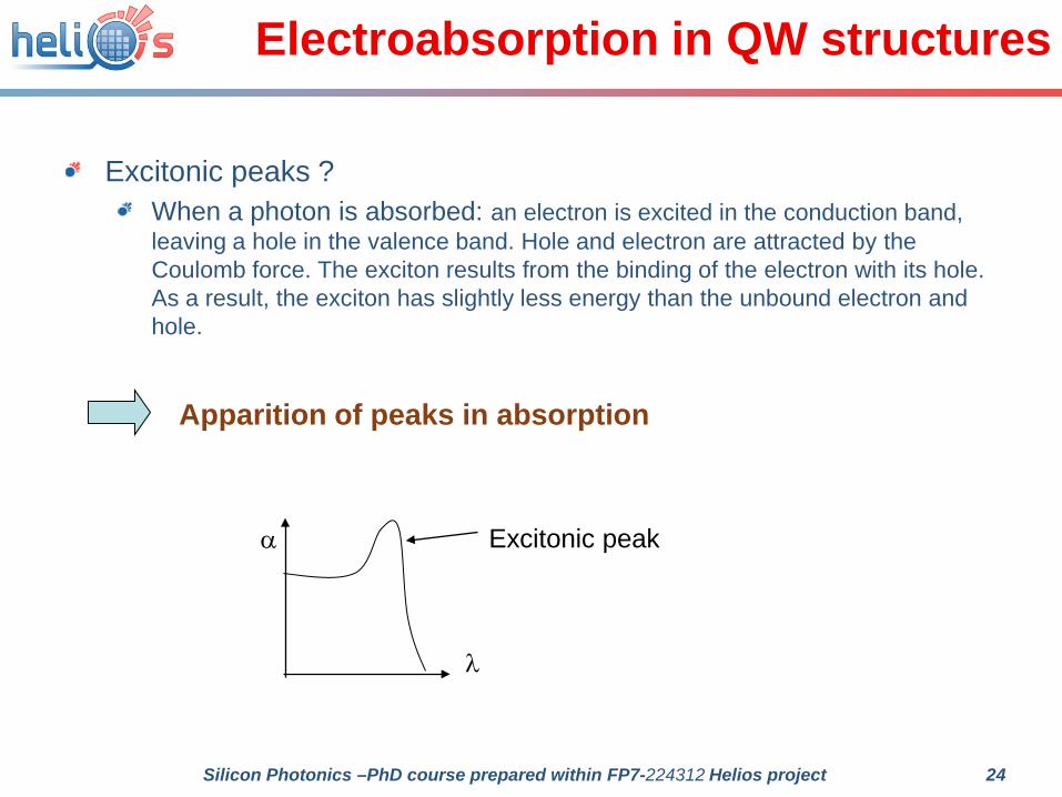
Electroabsorption in QW structures
Excitonic peaks ?When a photon is absorbed: an electron is excited in the conduction band, leaving a hole in the valence band. Hole and electron are attracted by the Coulomb force. The exciton results from the binding of the electron with its hole. As a result, the exciton has slightly less energy than the unbound electron and hole.
Apparition of peaks in absorption
λ
Excitonic peakα
25Silicon Photonics –PhD course prepared within FP7-224312 Helios project
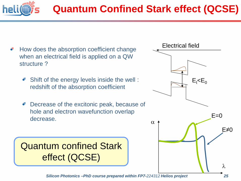
Quantum Confined Stark effect (QCSE)
How does the absorption coefficient change when an electrical field is applied on a QW structure ?
Shift of the energy levels inside the well : redshift of the absorption coefficient
Decrease of the excitonic peak, because of hole and electron wavefunction overlap decrease.
Electrical field
Et<E0
α
λ
E=0
E≠0
Quantum confined Stark effect (QCSE)
26Silicon Photonics –PhD course prepared within FP7-224312 Helios project
Quantum Confined Stark effect (QCSE)
Direct bandgap SC (III-V materials)QCSE is more efficient than Franz Keldysh effect (a larger absorption coefficient is generally obtained.Well thickness is modified to tune the absorption edge wavelengthIntrinsically high speed process
Integration of QCSE modulator on silicon ?
QCSE in group IV materials ?
27Silicon Photonics –PhD course prepared within FP7-224312 Helios project
Quantum Confined Stark effect (QCSE)
Integration of III-V QCSE modulator on silicon:
Hybrid silicon evanescent electroabsorption modulator AlGaInAs quantum wells Extinction ratio over 10dB, modulation bandwidth of 10 GHz. Open eye at 10Gb/s
Kuo et al., Opt. Express 16, 9936 (2008)
28Silicon Photonics –PhD course prepared within FP7-224312 Helios project
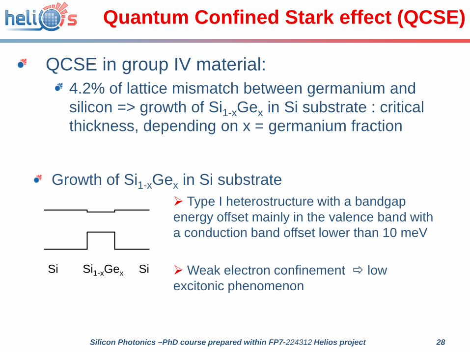
Quantum Confined Stark effect (QCSE)
QCSE in group IV material:4.2% of lattice mismatch between germanium and silicon => growth of Si1-xGex in Si substrate : critical thickness, depending on x = germanium fraction
Growth of Si1-xGex in Si substrate Type I heterostructure with a bandgap energy offset mainly in the valence band with a conduction band offset lower than 10 meV
Weak electron confinement low excitonic phenomenon
Si Si1-xGex Si
29Silicon Photonics –PhD course prepared within FP7-224312 Helios project
Quantum Confined Stark Effect
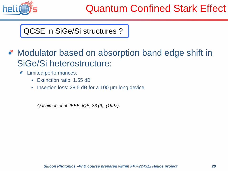
Qasaimeh et al IEEE JQE, 33 (9), (1997).
QCSE in SiGe/Si structures ?
Modulator based on absorption band edge shift in SiGe/Si heterostructure:
Limited performances: • Extinction ratio: 1.55 dB• Insertion loss: 28.5 dB for a 100 µm long device
30Silicon Photonics –PhD course prepared within FP7-224312 Helios project
Quantum Confined Stark Effect
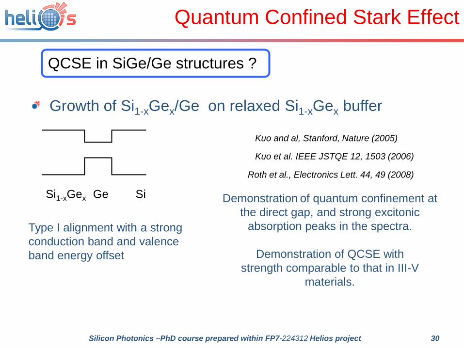
QCSE in SiGe/Ge structures ?
Kuo and al, Stanford, Nature (2005)
Kuo et al. IEEE JSTQE 12, 1503 (2006)
Growth of Si1-xGex/Ge on relaxed Si1-xGex buffer
Si1-xGex Ge Si Demonstration of quantum confinement at the direct gap, and strong excitonic
absorption peaks in the spectra.
Demonstration of QCSE withstrength comparable to that in III-V
materials.
Type I alignment with a strong conduction band and valence band energy offset
Roth et al., Electronics Lett. 44, 49 (2008)
31Silicon Photonics –PhD course prepared within FP7-224312 Helios project
Electroabsorption silicon based modulators
Homogeneous GeSi: Franz-Keldysh effect:10-dB extinction ratio at 1.540 nmOperating spectrum range of about 1.539–1.553 µm3-dB bandwidth of 1.2 GHz
Integration of III-V on silicon Hybrid silicon evanescent modulatorExtinction ratio over 10dB, modulation bandwidth of 10 GHz. Open eye at 10 Gb/s
Si/Si1-xGex quantum well: Quantum confined Stark effectweak effect: low electron confinement in the wellLimited performances
Si1-xGex/Ge quantum well : Quantum confined Stark effect3 dB modulation possible with 1 V swingFundamental limit to speed ~ 1 ps
32Silicon Photonics –PhD course prepared within FP7-224312 Helios project
Outline
I-Introduction :Optical modulationFigure of merits
II-Mechanisms for Optical Modulation in group IV materials (Si, Ge)ElectroabsorptionElectrorefractionFree carrier concentration variation
III-Waveguide integrated silicon optical modulator using free carrier concentration variations
Waveguide integrated optical modulator considerationsSilicon optical modulators using free carrier concentration variations:
• Carrier injection in PIN diode• Carrier shifts in Bipolar Mode Field Effect Transistor• Carriers accumulation in Metal Oxyde Semiconductor capacitors• Carrier depletion in PN/PIN diode
33Silicon Photonics –PhD course prepared within FP7-224312 Helios project
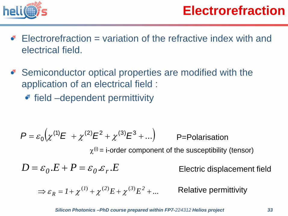
Electrorefraction
Electrorefraction = variation of the refractive index with and electrical field.
Semiconductor optical properties are modified with the application of an electrical field :
field –dependent permittivity
( )...3)3(2)2()1(0 +++= EEEP χχχε
χ(i) = i-order component of the susceptibility (tensor)
...)()()( ++++=⇒ 2321R EE1 χχχε
EPED r00 ... εεε =+=
Relative permittivity
P=Polarisation
Electric displacement field
34Silicon Photonics –PhD course prepared within FP7-224312 Helios project
Electrorefraction
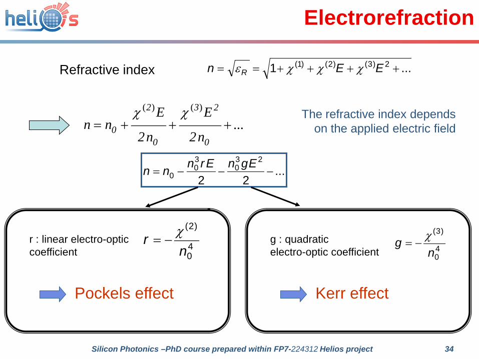
...1 2)3()2()1( ++++== EEn R χχχε
...)()(
+++=0
23
0
2
0 n2
E
n2
Enn
χχ The refractive index depends on the applied electric field
Refractive index
...22
230
30
0 −−−=EgnErnnn
40
)3(
ng χ
−=
Pockels effect
40
)2(
nr χ
−=r : linear electro-optic coefficient
Kerr effect
g : quadratic electro-optic coefficient
35Silicon Photonics –PhD course prepared within FP7-224312 Helios project
Electrorefraction
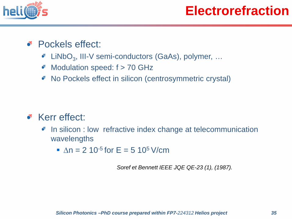
Pockels effect:LiNbO3, III-V semi-conductors (GaAs), polymer, …Modulation speed: f > 70 GHz No Pockels effect in silicon (centrosymmetric crystal)
Soref et Bennett IEEE JQE QE-23 (1), (1987).
Kerr effect:In silicon : low refractive index change at telecommunication wavelengths ∆n = 2 10-5 for E = 5 105 V/cm
36Silicon Photonics –PhD course prepared within FP7-224312 Helios project
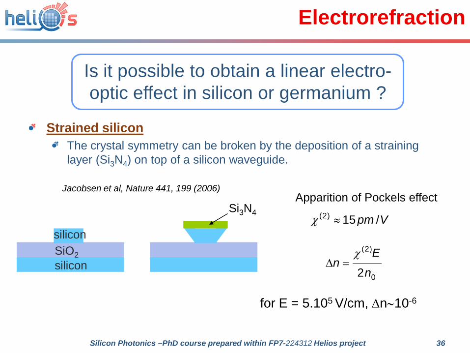
Electrorefraction
Is it possible to obtain a linear electro-optic effect in silicon or germanium ?
Strained siliconThe crystal symmetry can be broken by the deposition of a straining layer (Si3N4) on top of a silicon waveguide.
Vpm /15)2( ≈χ
0
)2(
2n
En
χ=∆silicon
SiO2
silicon
Si3N4
Apparition of Pockels effect
for E = 5.105 V/cm, ∆n∼10-6
Jacobsen et al, Nature 441, 199 (2006)
37Silicon Photonics –PhD course prepared within FP7-224312 Helios project
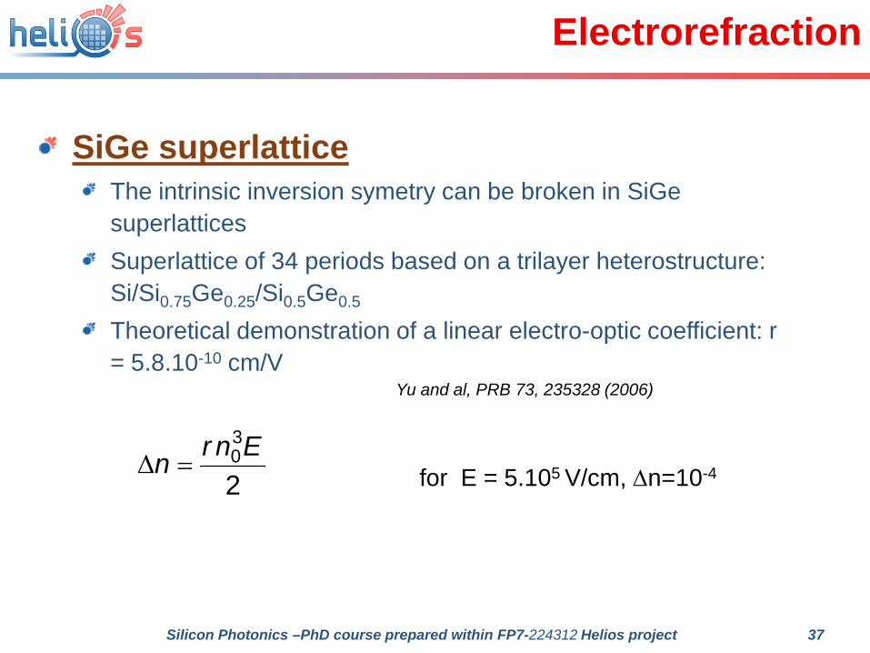
Electrorefraction
2
30Enrn =∆
Yu and al, PRB 73, 235328 (2006)
for E = 5.105 V/cm, ∆n=10-4
SiGe superlatticeThe intrinsic inversion symetry can be broken in SiGe superlatticesSuperlattice of 34 periods based on a trilayer heterostructure: Si/Si0.75Ge0.25/Si0.5Ge0.5
Theoretical demonstration of a linear electro-optic coefficient: r = 5.8.10-10 cm/V
38Silicon Photonics –PhD course prepared within FP7-224312 Helios project
Electrorefraction
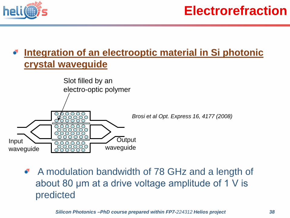
Integration of an electrooptic material in Si photonic crystal waveguide
A modulation bandwidth of 78 GHz and a length of about 80 μm at a drive voltage amplitude of 1 V is predicted
Slot filled by an electro-optic polymer
Brosi et al Opt. Express 16, 4177 (2008)
Input waveguide
Output waveguide
39Silicon Photonics –PhD course prepared within FP7-224312 Helios project
Outline
I-Introduction :Optical modulationFigure of merits
II-Mechanisms for Optical Modulation in group IV materials (Si, Ge)ElectroabsorptionElectrorefractionFree carrier concentration variation
III-Waveguide integrated silicon optical modulator using free carrier concentration variations
Waveguide integrated optical modulator considerationsSilicon optical modulators using free carrier concentration variations:
• Carrier injection in PIN diode• Carrier shifts in Bipolar Mode Field Effect Transistor• Carriers accumulation in Metal Oxyde Semiconductor capacitors• Carrier depletion in PN/PIN diode
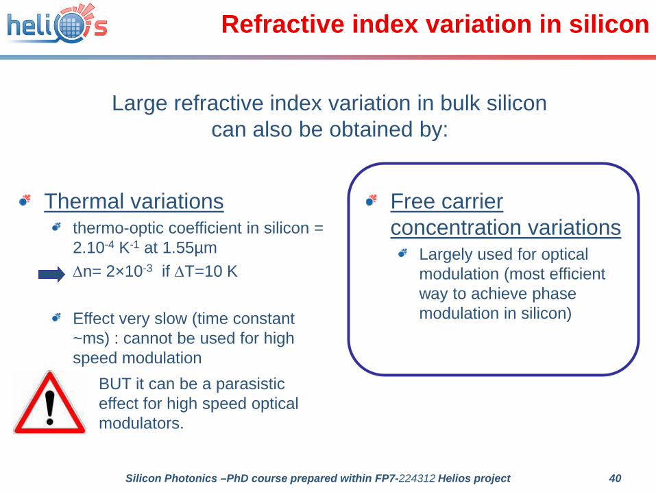
40Silicon Photonics –PhD course prepared within FP7-224312 Helios project
Refractive index variation in silicon
Large refractive index variation in bulk silicon can also be obtained by:
Thermal variationsthermo-optic coefficient in silicon = 2.10-4 K-1 at 1.55µm∆n= 2×10⁻³ if ∆T=10 K
Effect very slow (time constant ~ms) : cannot be used for high speed modulation
BUT it can be a parasistic effect for high speed optical modulators.
Free carrier concentration variations
Largely used for optical modulation (most efficient way to achieve phase modulation in silicon)
41Silicon Photonics –PhD course prepared within FP7-224312 Helios project
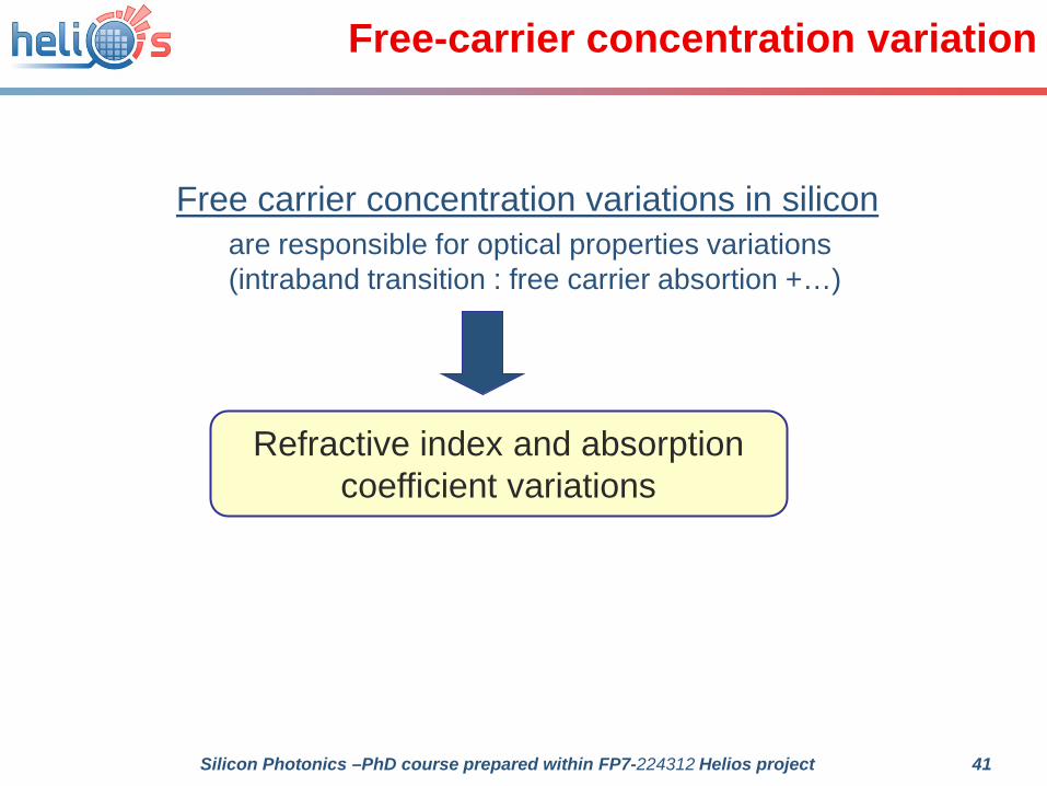
Free-carrier concentration variation
Free carrier concentration variations in siliconare responsible for optical properties variations (intraband transition : free carrier absortion +…)
Refractive index and absorption coefficient variations
42Silicon Photonics –PhD course prepared within FP7-224312 Helios project
Free-carrier concentration variation
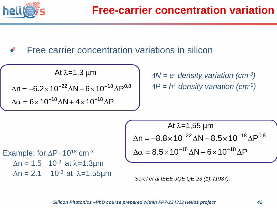
Free carrier concentration variations in silicon
∆N = e- density variation (cm-3)∆P = h+ density variation (cm-3)
Example: for ∆P=1018 cm-3
∆n = 1.5 10-3 at λ=1.3µm ∆n = 2.1 10-3 at λ=1.55µm
P104N106
P106N102.6n1818
8,01822
∆×+∆×=α∆
∆×−∆×−=∆−−
−−
At λ=1,3 µm
P106N105.8
P105.8N108.8n1818
8,01822
∆×+∆×=α∆
∆×−∆×−=∆−−
−−
At λ=1,55 µm
Soref et al IEEE JQE QE-23 (1), (1987).

43Silicon Photonics –PhD course prepared within FP7-224312 Helios project
Free-carrier concentration variation
How is it possible to obtain free carrier concentration variation in silicon?
Carrier injection in PN/PIN diode (forward bias)
Carrier plasma shift in bipolar mode field-effect transistor
(BMFET).
Carrier accumulation in MOS capacitor
Carrier depletion in PN/PIN diodes (reverse bias)
44Silicon Photonics –PhD course prepared within FP7-224312 Helios project
Free-carrier concentration variation
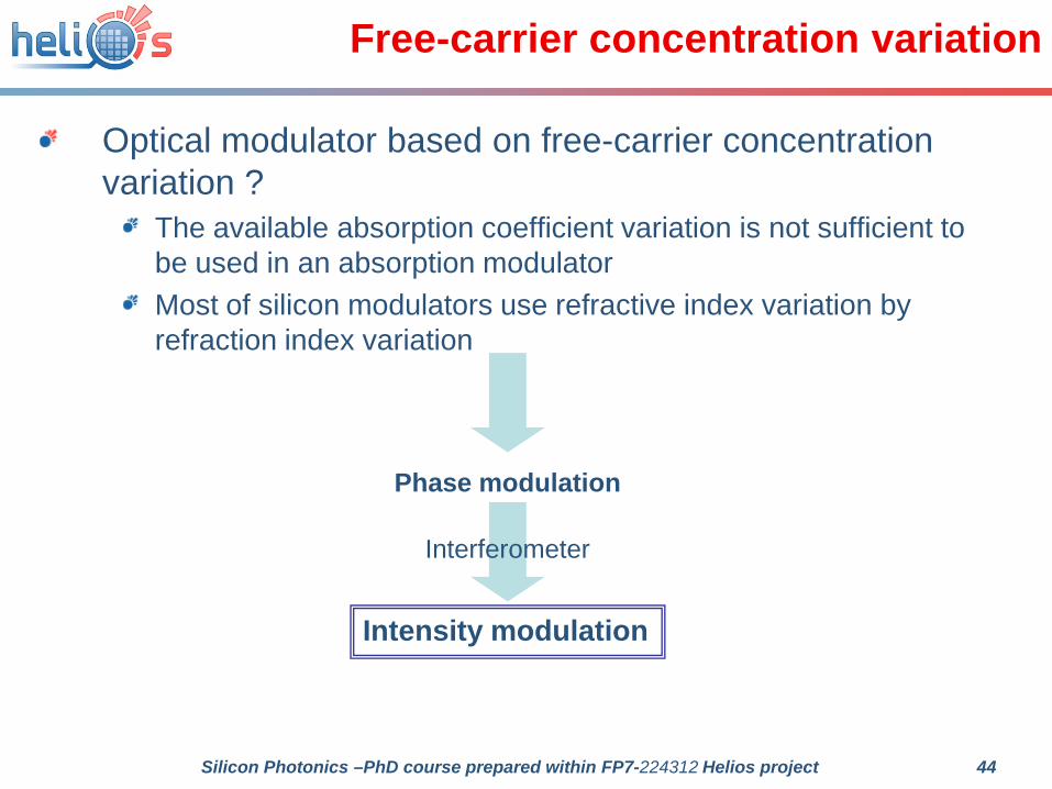
Optical modulator based on free-carrier concentration variation ?
The available absorption coefficient variation is not sufficient to be used in an absorption modulatorMost of silicon modulators use refractive index variation by refraction index variation
Phase modulation
Intensity modulation
Interferometer

45Silicon Photonics –PhD course prepared within FP7-224312 Helios project
Outline
I-Introduction :Optical modulationFigure of merits
II-Mechanisms for Optical Modulation in group IV materials (Si, Ge)ElectroabsorptionElectrorefractionFree carrier concentration variation
III-Waveguide integrated silicon optical modulator using free carrier concentration variations
Waveguide integrated optical modulator considerationsSilicon optical modulators using free carrier concentration variations:
• Carrier injection in PIN diode• Carrier shifts in Bipolar Mode Field Effect Transistor• Carriers accumulation in Metal Oxyde Semiconductor capacitors• Carrier depletion in PN/PIN diode
46Silicon Photonics –PhD course prepared within FP7-224312 Helios project
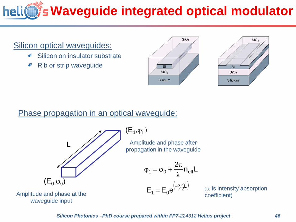
Waveguide integrated optical modulator
Phase propagation in an optical waveguide:
(E0,ϕ0)
(E1,ϕ1)
Amplitude and phase at the waveguide input
Amplitude and phase after propagation in the waveguide
L
Silicon optical waveguides:Silicon on insulator substrateRib or strip waveguide
Ln2eff01 λ
π+ϕ=ϕ
( )L201 eEE
α−= (α is intensity absorption
coefficient)
47Silicon Photonics –PhD course prepared within FP7-224312 Helios project
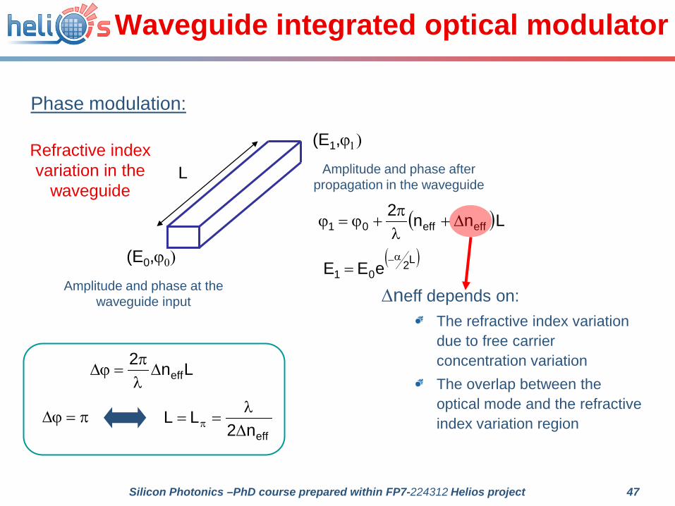
Waveguide integrated optical modulator
Phase modulation:
( )Lnn2effeff01 ∆+
λπ
+ϕ=ϕ
(E0,ϕ0)
(E1,ϕ1)
Amplitude and phase at the waveguide input
Amplitude and phase after propagation in the waveguide
LRefractive index variation in the
waveguide
∆neff depends on:The refractive index variation due to free carrier concentration variationThe overlap between the optical mode and the refractive index variation regionπ=ϕ∆
Ln2eff∆
λπ
=ϕ∆
effn2LL
∆λ
== π
( )L201 eEE
α−=
48Silicon Photonics –PhD course prepared within FP7-224312 Helios project
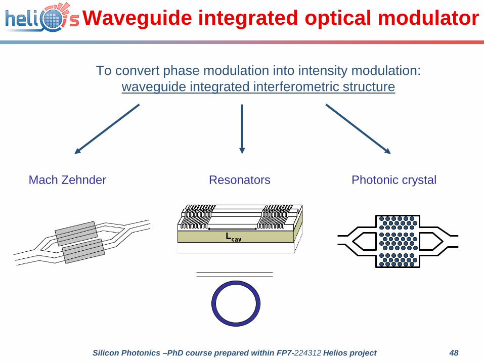
Waveguide integrated optical modulator
To convert phase modulation into intensity modulation: waveguide integrated interferometric structure
Mach Zehnder Resonators Photonic crystal
49Silicon Photonics –PhD course prepared within FP7-224312 Helios project
Waveguide integrated optical modulator
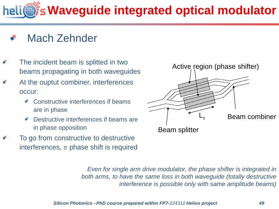
Mach Zehnder
The incident beam is splitted in two beams propagating in both waveguidesAt the ouptut combiner, interferences occur:
Constructive interferences if beams are in phaseDestructive interferences if beams are in phase opposition
To go from constructive to destructive interferences, π phase shift is required
Beam splitter
Beam combiner
Active region (phase shifter)
Even for single arm drive modulator, the phase shifter is integrated in both arms, to have the same loss in both waveguide (totally destructive
interference is possible only with same amplitude beams)
Lπ
50Silicon Photonics –PhD course prepared within FP7-224312 Helios project
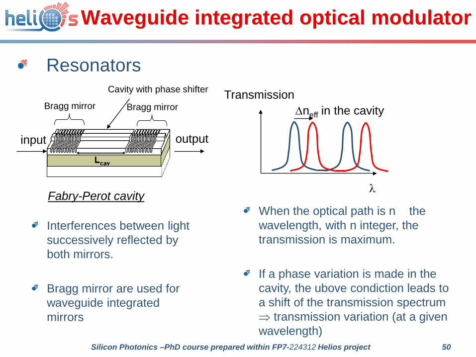
Waveguide integrated optical modulator
Resonators
Fabry-Perot cavity
Interferences between light successively reflected by both mirrors.
Bragg mirror are used for waveguide integrated mirrors
When the optical path is n the wavelength, with n integer, the transmission is maximum.
If a phase variation is made in the cavity, the ubove condiction leads to a shift of the transmission spectrum ⇒ transmission variation (at a given wavelength)
Bragg mirror Bragg mirror
Cavity with phase shifter
input output
λ
Transmission∆neff in the cavity
51Silicon Photonics –PhD course prepared within FP7-224312 Helios project
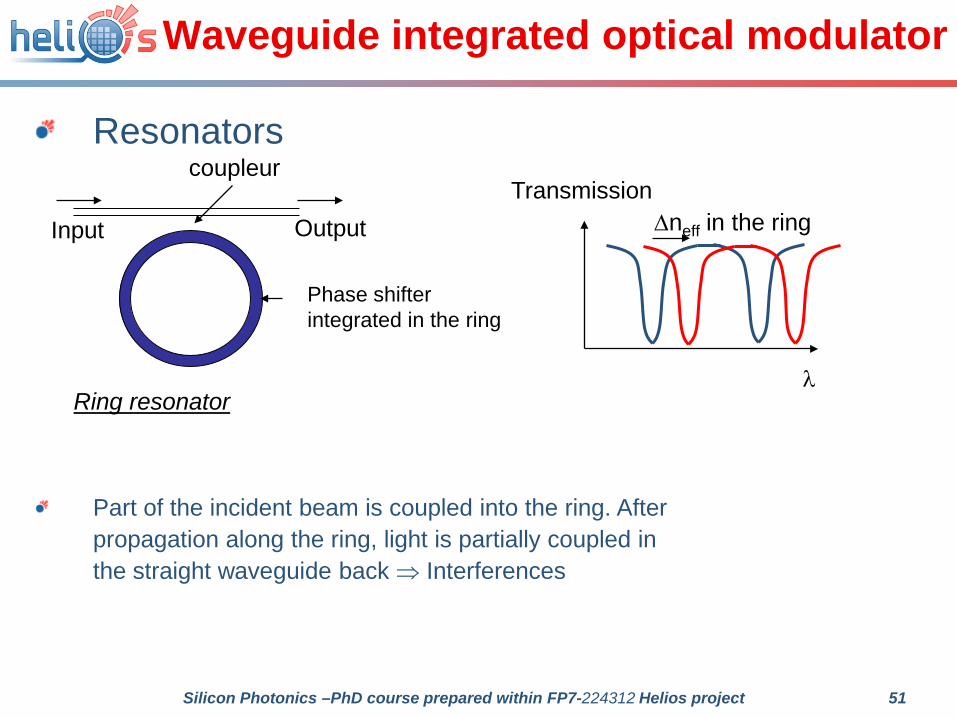
Waveguide integrated optical modulator
Resonators
Input Output
coupleur
Ring resonator
Part of the incident beam is coupled into the ring. After propagation along the ring, light is partially coupled in the straight waveguide back ⇒ Interferences
Phase shifter integrated in the ring
λ
Transmission∆neff in the ring
52Silicon Photonics –PhD course prepared within FP7-224312 Helios project
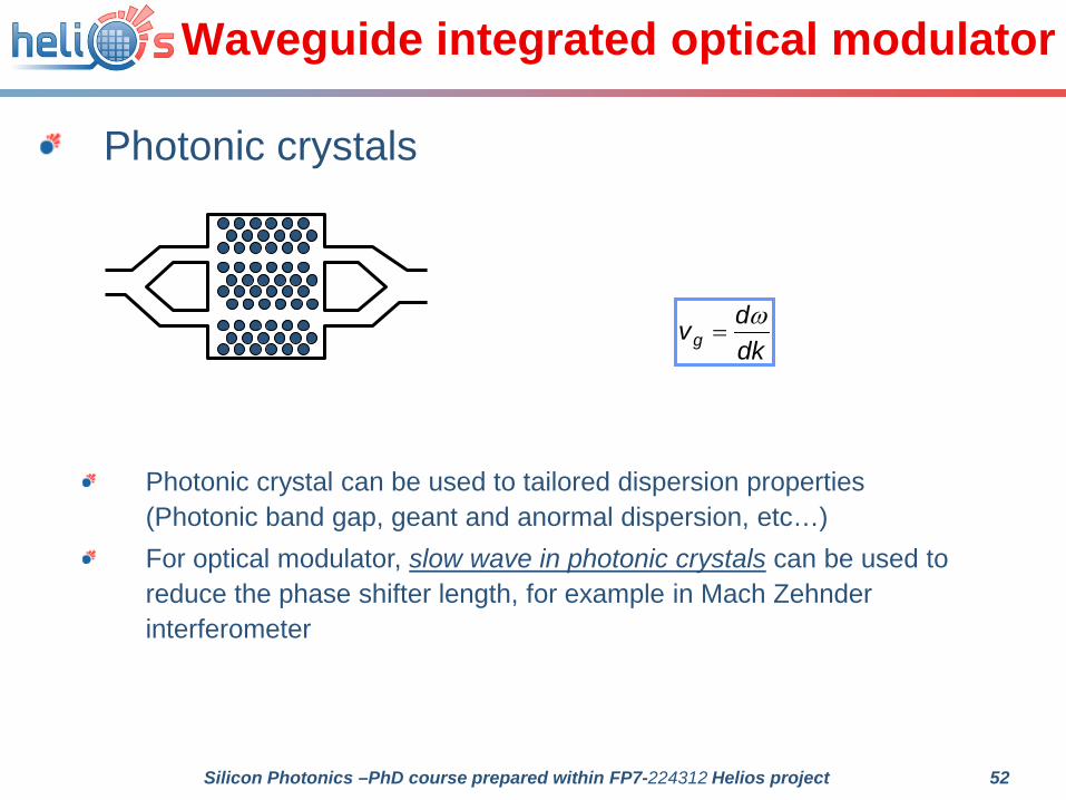
Waveguide integrated optical modulator
Photonic crystals
Photonic crystal can be used to tailored dispersion properties (Photonic band gap, geant and anormal dispersion, etc…)For optical modulator, slow wave in photonic crystals can be used to reduce the phase shifter length, for example in Mach Zehnder interferometer
dkdvg
ω=

53Silicon Photonics –PhD course prepared within FP7-224312 Helios project
Waveguide integrated optical modulator
( )Lnn2effeff01 ∆+
λπ
+ϕ=ϕ
(E0,ϕ0)
(E1,ϕ1)
Amplitude and phase at the waveguide input
Amplitude and phase after propagation in the waveguide
LRefractive index and absorption
coefficient variations in the
waveguide
Refractive index variation goes along with absorption coefficient variation:
( )
α∆+α−
=L2
01 eEE
This can be a parasitic effect, for example:• when using Mach Zehdner interferometer, if the output field amplitudes are not the same, interference cannot be entirelly destructive, and Imin ≠0 at the modulator output)•In resonators absorption increase is responsible for mimimum transmission increase
54Silicon Photonics –PhD course prepared within FP7-224312 Helios project
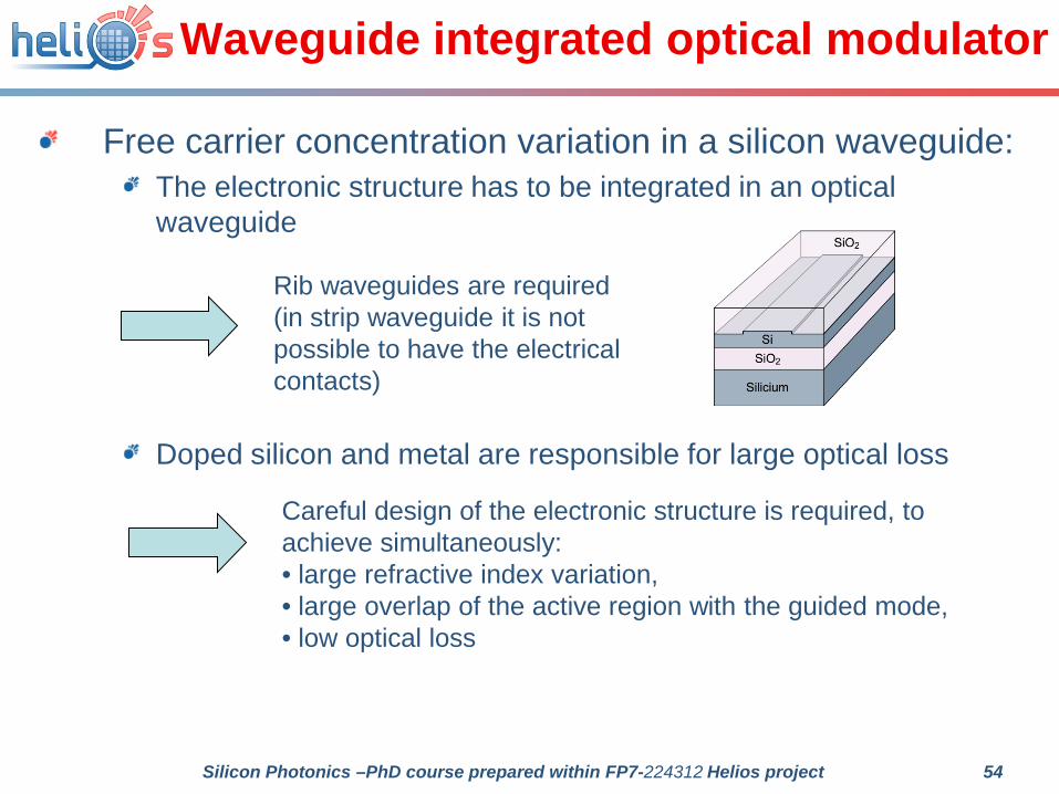
Waveguide integrated optical modulator
Free carrier concentration variation in a silicon waveguide:The electronic structure has to be integrated in an optical waveguide
Rib waveguides are required(in strip waveguide it is not possible to have the electrical contacts)
Doped silicon and metal are responsible for large optical loss
Careful design of the electronic structure is required, to achieve simultaneously:• large refractive index variation,• large overlap of the active region with the guided mode, • low optical loss

55Silicon Photonics –PhD course prepared within FP7-224312 Helios project
Outline
I-Introduction :Optical modulationFigure of merits
II-Mechanisms for Optical Modulation in group IV materials (Si, Ge)ElectroabsorptionElectrorefractionFree carrier concentration variation
III-Waveguide integrated silicon optical modulator using free carrier concentration variations
Waveguide integrated optical modulator considerationsSilicon optical modulators using free carrier concentration variations:
• Carrier injection in PIN diode• Carrier shifts in Bipolar Mode Field Effect Transistor• Carriers accumulation in Metal Oxyde Semiconductor capacitors• Carrier depletion in PN/PIN diode
56Silicon Photonics –PhD course prepared within FP7-224312 Helios project
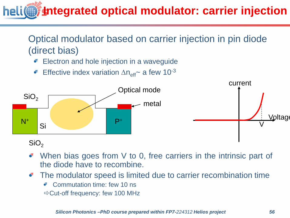
Integrated optical modulator: carrier injection
Optical modulator based on carrier injection in pin diode (direct bias)
Electron and hole injection in a waveguideEffective index variation ∆neff~ a few 10-3
P+N+Si
SiO2
Optical mode
SiO2
When bias goes from V to 0, free carriers in the intrinsic part ofthe diode have to recombine.The modulator speed is limited due to carrier recombination time
Commutation time: few 10 nsCut-off frequency: few 100 MHz
Voltage
current
V
metal

57Silicon Photonics –PhD course prepared within FP7-224312 Helios project
Integrated optical modulator: carrier injection
Optical modulator based on carrier injection in pin diode (direct bias)
To increase the speed:• Direct and reverse biasing
voltage
current
V1 V2
Barrios et al JLT 21(10) 2003
Theoretically:Switching time = 1.3 ns for V1=-1 and V2=0.87 V∆neff~ 10-3
58Silicon Photonics –PhD course prepared within FP7-224312 Helios project
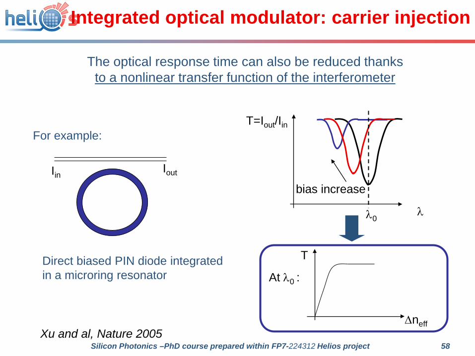
Integrated optical modulator: carrier injection
The optical response time can also be reduced thanks to a nonlinear transfer function of the interferometer
Direct biased PIN diode integrated in a microring resonator
IoutIin
λ
T=Iout/Iin
λ0
bias increase
For example:
∆neff
T
At λ0 :
Xu and al, Nature 2005
59Silicon Photonics –PhD course prepared within FP7-224312 Helios project
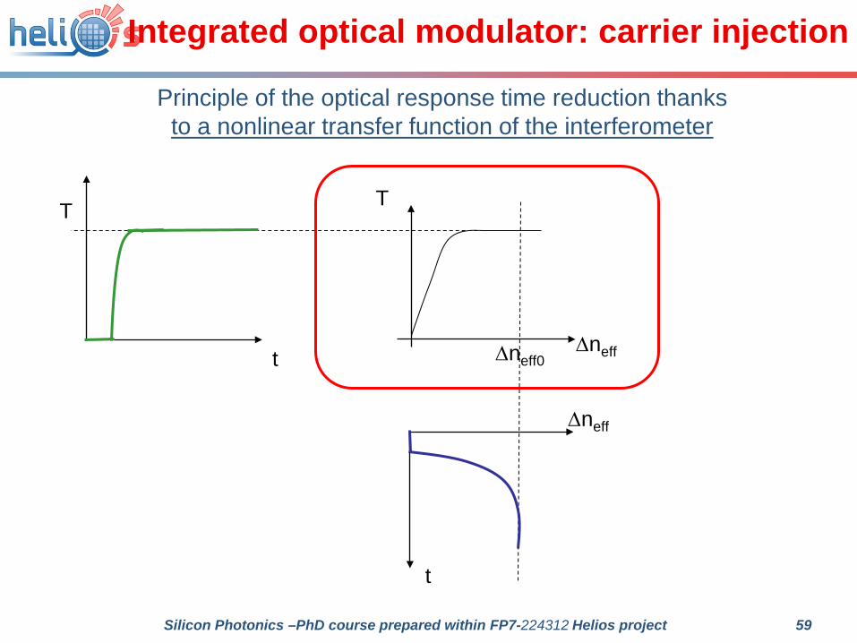
Integrated optical modulator: carrier injection
Principle of the optical response time reduction thanks to a nonlinear transfer function of the interferometer
T
t∆neff
T
∆neff0
∆neff
t
60Silicon Photonics –PhD course prepared within FP7-224312 Helios project
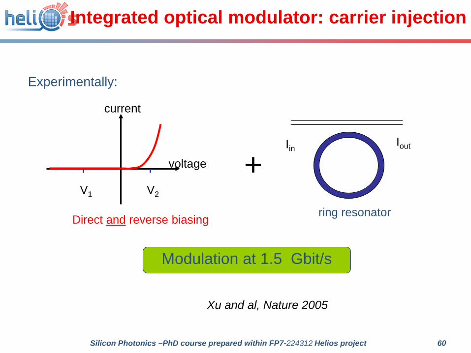
Integrated optical modulator: carrier injection
Xu and al, Nature 2005
Experimentally:
voltage
current
V1 V2
+
Modulation at 1.5 Gbit/s
IoutIin
Direct and reverse biasing ring resonator
61Silicon Photonics –PhD course prepared within FP7-224312 Helios project
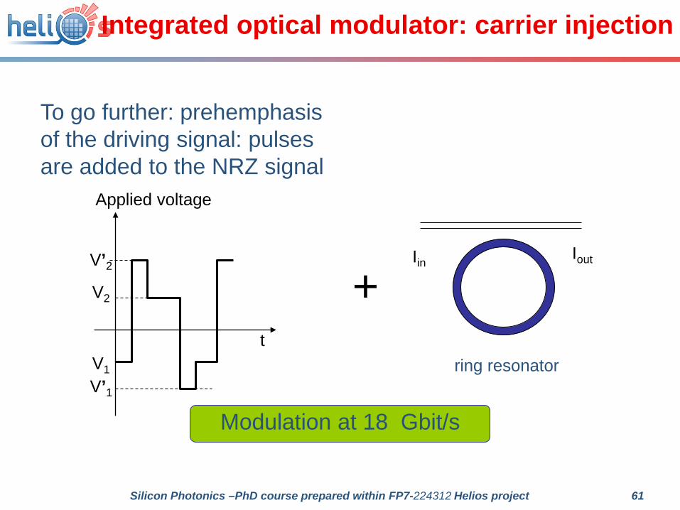
Integrated optical modulator: carrier injection
To go further: prehemphasis of the driving signal: pulses are added to the NRZ signal
Applied voltage
V2
V’1
V’2
V1
t
+ IoutIin
Modulation at 18 Gbit/s
ring resonator
62Silicon Photonics –PhD course prepared within FP7-224312 Helios project
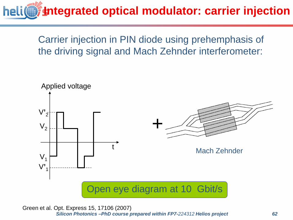
Integrated optical modulator: carrier injection
Carrier injection in PIN diode using prehemphasis of the driving signal and Mach Zehnder interferometer:
Applied voltage
V2
V’1
V’2
V1
t
+
Open eye diagram at 10 Gbit/s
Green et al. Opt. Express 15, 17106 (2007)
Mach Zehnder

63Silicon Photonics –PhD course prepared within FP7-224312 Helios project
Outline
I-Introduction :Optical modulationFigure of merits
II-Mechanisms for Optical Modulation in group IV materials (Si, Ge)ElectroabsorptionElectrorefractionFree carrier concentration variation
III-Waveguide integrated silicon optical modulator using free carrier concentration variations
Waveguide integrated optical modulator considerationsSilicon optical modulators using free carrier concentration variations:
• Carrier injection in PIN diode• Carrier shifts in Bipolar Mode Field Effect Transistor• Carriers accumulation in Metal Oxyde Semiconductor capacitors• Carrier depletion in PN/PIN diode
64Silicon Photonics –PhD course prepared within FP7-224312 Helios project
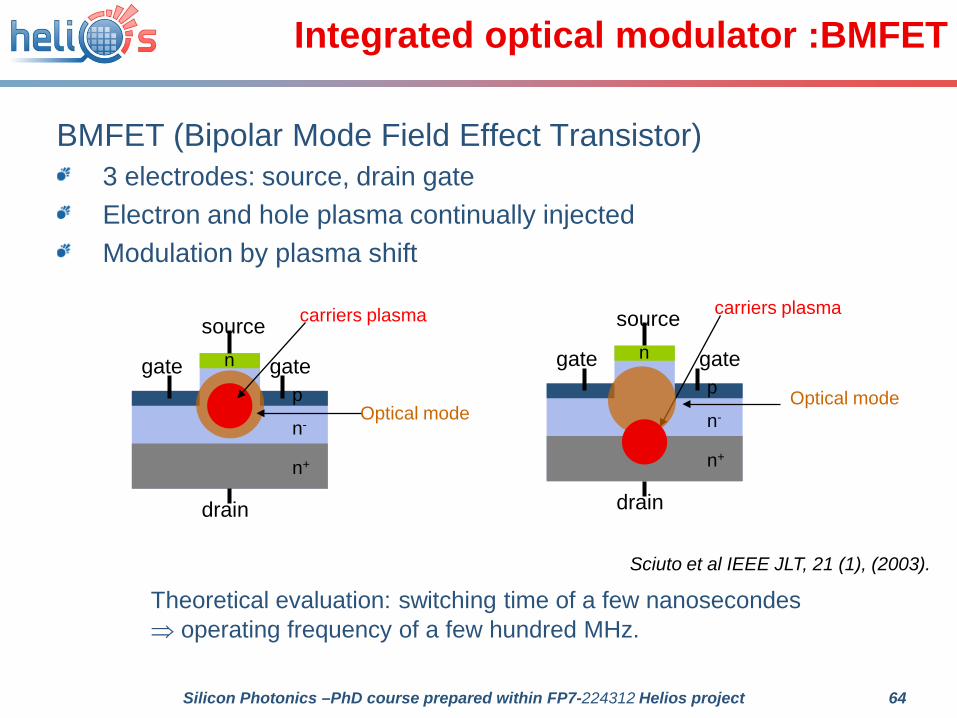
Integrated optical modulator :BMFET
BMFET (Bipolar Mode Field Effect Transistor)3 electrodes: source, drain gateElectron and hole plasma continually injectedModulation by plasma shift
Sciuto et al IEEE JLT, 21 (1), (2003).
Theoretical evaluation: switching time of a few nanosecondes⇒ operating frequency of a few hundred MHz.
n
p
n-
n+
gate gate
source
drain
carriers plasma
Optical mode
n
p
n-
n+
gate gate
source
drain
carriers plasma
Optical mode
65Silicon Photonics –PhD course prepared within FP7-224312 Helios project
Outline
I-Introduction :Optical modulationFigure of merits
II-Mechanisms for Optical Modulation in group IV materials (Si, Ge)ElectroabsorptionElectrorefractionFree carrier concentration variation
III-Waveguide integrated silicon optical modulator using free carrier concentration variations
Waveguide integrated optical modulator considerationsSilicon optical modulators using free carrier concentration variations:
• Carrier injection in PIN diode• Carrier shifts in Bipolar Mode Field Effect Transistor• Carriers accumulation in Metal Oxyde Semiconductor capacitors• Carrier depletion in PN/PIN diode
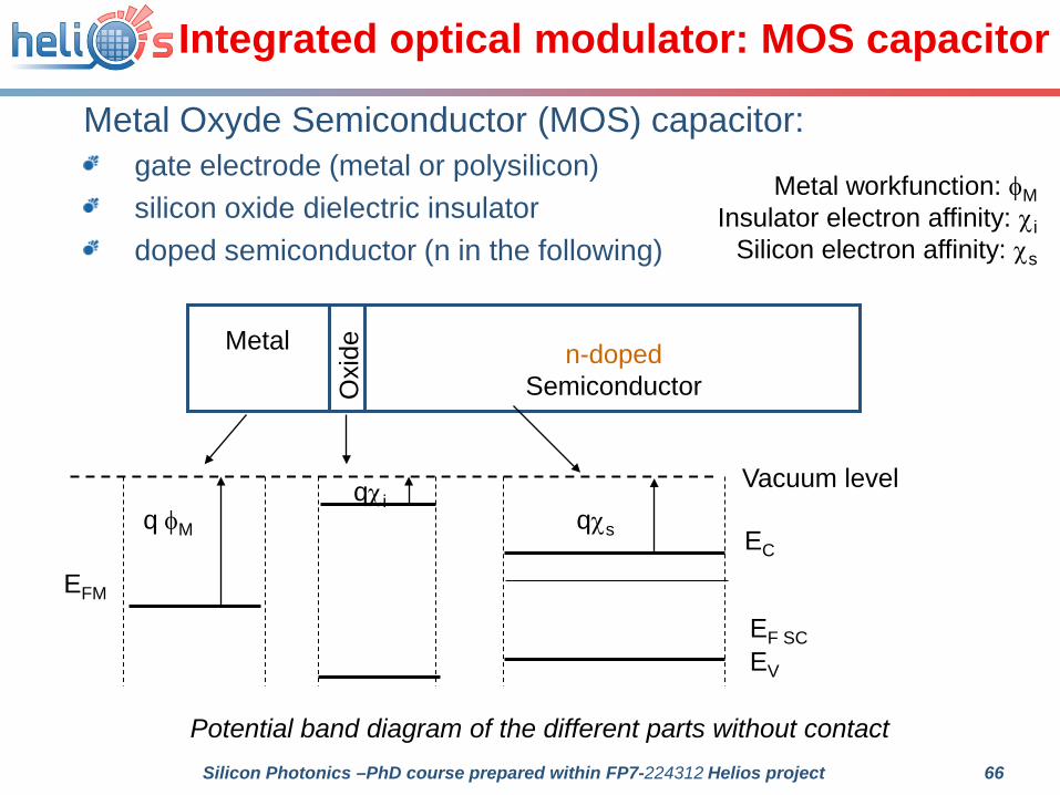
66Silicon Photonics –PhD course prepared within FP7-224312 Helios project
Integrated optical modulator: MOS capacitor
Metal workfunction: φMInsulator electron affinity: χi
Silicon electron affinity: χs
Vacuum level
EFM
EC
EV
EF SC
qχiq φM qχs
MetalO
xide n-doped
Semiconductor
Metal Oxyde Semiconductor (MOS) capacitor:gate electrode (metal or polysilicon)silicon oxide dielectric insulatordoped semiconductor (n in the following)
Potential band diagram of the different parts without contact
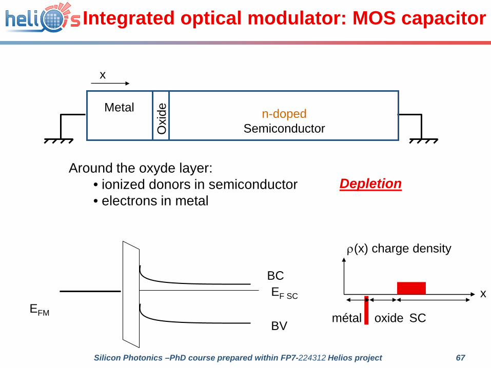
67Silicon Photonics –PhD course prepared within FP7-224312 Helios project
Integrated optical modulator: MOS capacitor
Around the oxyde layer:• ionized donors in semiconductor• electrons in metal
EFM
BC
BV
EF SC
Depletion
Metal
Oxi
de n-doped Semiconductor
ρ(x) charge density
x
oxide SCmétal
x
68Silicon Photonics –PhD course prepared within FP7-224312 Helios project
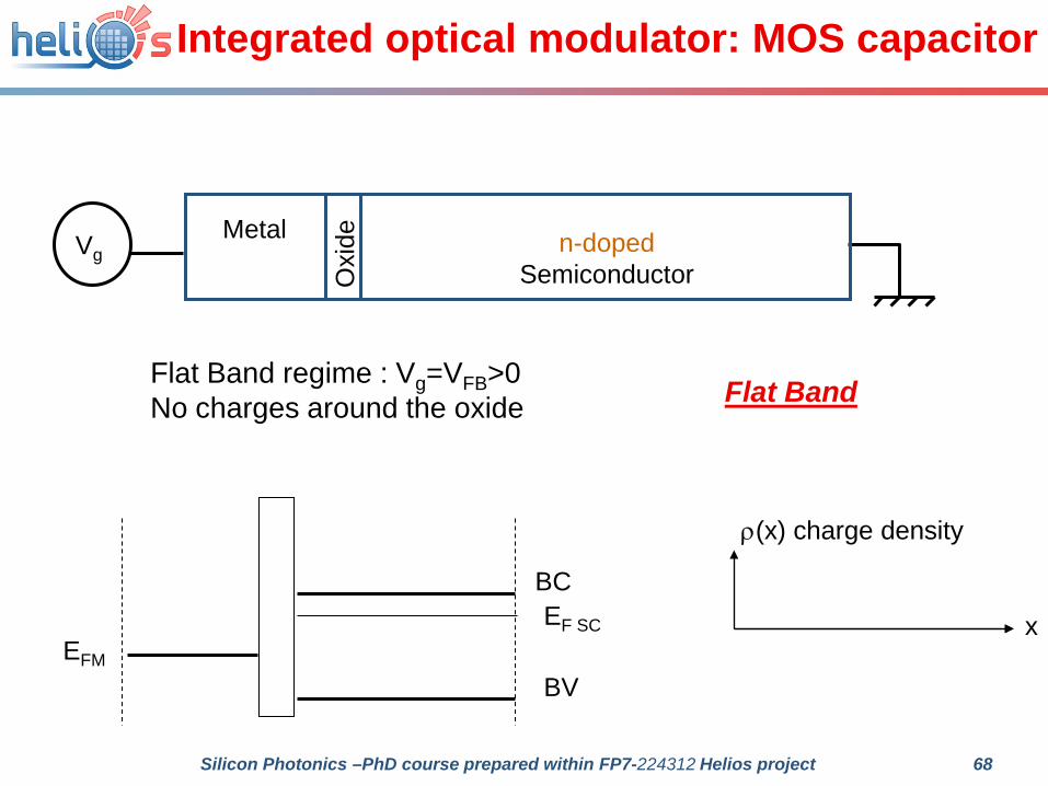
Integrated optical modulator: MOS capacitor
Flat Band regime : Vg=VFB>0No charges around the oxide
Vg
EFM
BC
BV
EF SC x
Metal
Oxi
de n-doped Semiconductor
ρ(x) charge density
Flat Band
69Silicon Photonics –PhD course prepared within FP7-224312 Helios project
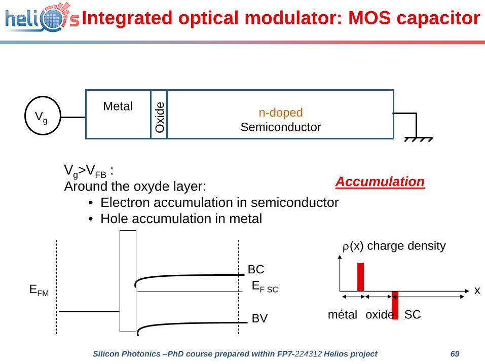
Integrated optical modulator: MOS capacitor
EFM
BC
BV
EF SC
Vg>VFB : Around the oxyde layer:
• Electron accumulation in semiconductor• Hole accumulation in metal
Accumulation
Metal
Oxi
de n-doped Semiconductor
ρ(x) charge density
x
oxide SCmétal
Vg
70Silicon Photonics –PhD course prepared within FP7-224312 Helios project
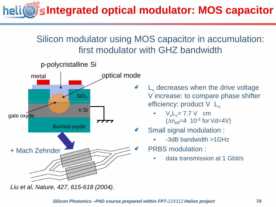
Integrated optical modulator: MOS capacitor
Silicon modulator using MOS capacitor in accumulation: first modulator with GHZ bandwidth
Liu et al, Nature, 427, 615-618 (2004).
Lπ decreases when the drive voltage V increase: to compare phase shifter efficiency: product V Lπ
• VπLπ= 7.7 V cm (∆neff=4 10-5 for Vd=4V)
Small signal modulation : • -3dB bandwidth >1GHz
PRBS modulation : • data transmission at 1 Gbit/s
n Si
metal
Burried oxyde
SiO2
gate oxyde
p-polycristalline Sioptical mode
+ Mach Zehnder
71Silicon Photonics –PhD course prepared within FP7-224312 Helios project
Integrated optical modulator: MOS capacitor
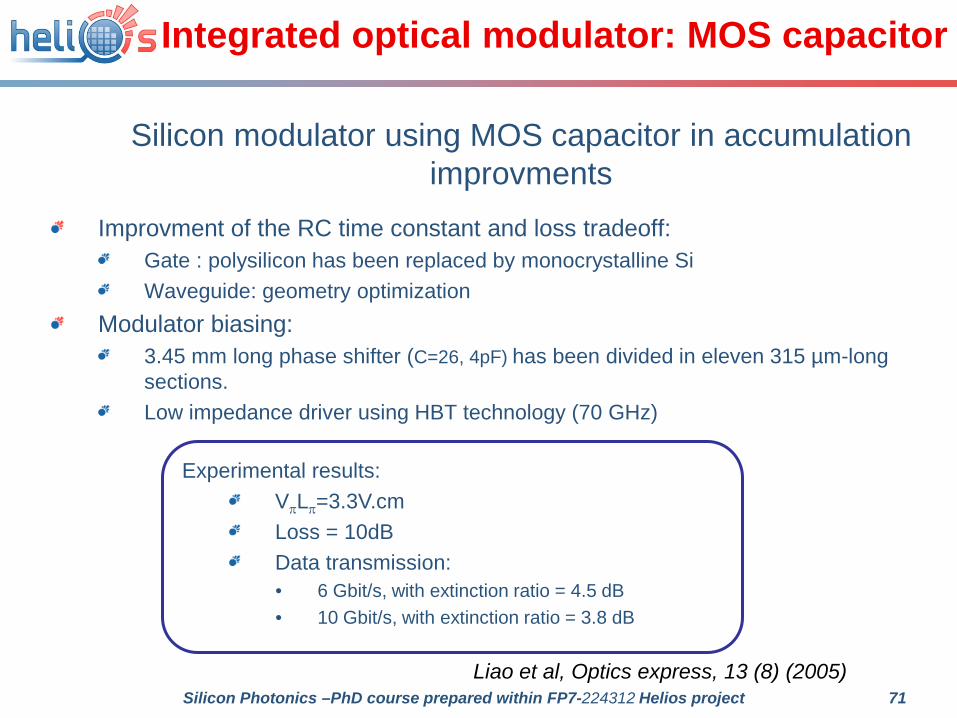
Silicon modulator using MOS capacitor in accumulation improvments
Improvment of the RC time constant and loss tradeoff:Gate : polysilicon has been replaced by monocrystalline SiWaveguide: geometry optimization
Modulator biasing:3.45 mm long phase shifter (C=26, 4pF) has been divided in eleven 315 µm-long sections.Low impedance driver using HBT technology (70 GHz)
Liao et al, Optics express, 13 (8) (2005)
Experimental results:VπLπ=3.3V.cm Loss = 10dBData transmission:• 6 Gbit/s, with extinction ratio = 4.5 dB• 10 Gbit/s, with extinction ratio = 3.8 dB
72Silicon Photonics –PhD course prepared within FP7-224312 Helios project
Outline
I-Introduction :Optical modulationFigure of merits
II-Mechanisms for Optical Modulation in group IV materials (Si, Ge)ElectroabsorptionElectrorefractionFree carrier concentration variation
III-Waveguide integrated silicon optical modulator using free carrier concentration variations
Waveguide integrated optical modulator considerationsSilicon optical modulators using free carrier concentration variations:
• Carrier injection in PIN diode• Carrier shifts in Bipolar Mode Field Effect Transistor• Carriers accumulation in Metal Oxyde Semiconductor capacitors• Carrier depletion in PN/PIN diode
73Silicon Photonics –PhD course prepared within FP7-224312 Helios project
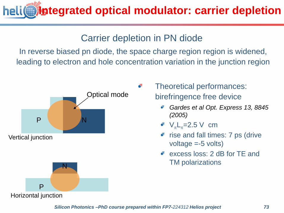
Integrated optical modulator: carrier depletion
Carrier depletion in PN diodeIn reverse biased pn diode, the space charge region region is widened,
leading to electron and hole concentration variation in the junction region
Theoretical performances: birefringence free device
Gardes et al Opt. Express 13, 8845 (2005)VπLπ=2.5 V cmrise and fall times: 7 ps (drive voltage =-5 volts)excess loss: 2 dB for TE and TM polarizations
P N
Optical mode
Vertical junction
P
N
Horizontal junction
74Silicon Photonics –PhD course prepared within FP7-224312 Helios project
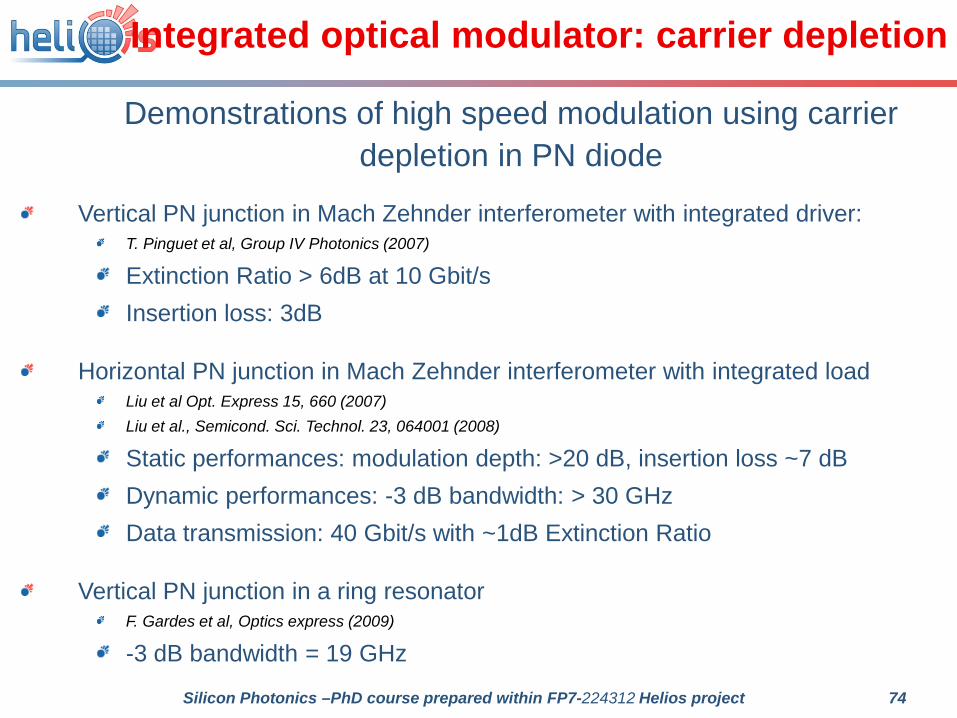
Integrated optical modulator: carrier depletion
Demonstrations of high speed modulation using carrier depletion in PN diode
Vertical PN junction in Mach Zehnder interferometer with integrated driver:T. Pinguet et al, Group IV Photonics (2007)
Extinction Ratio > 6dB at 10 Gbit/sInsertion loss: 3dB
Horizontal PN junction in Mach Zehnder interferometer with integrated loadLiu et al Opt. Express 15, 660 (2007)Liu et al., Semicond. Sci. Technol. 23, 064001 (2008)
Static performances: modulation depth: >20 dB, insertion loss ~7 dBDynamic performances: -3 dB bandwidth: > 30 GHzData transmission: 40 Gbit/s with ~1dB Extinction Ratio
Vertical PN junction in a ring resonatorF. Gardes et al, Optics express (2009)
-3 dB bandwidth = 19 GHz

75Silicon Photonics –PhD course prepared within FP7-224312 Helios project
Integrated optical modulator: carrier depletion
Carrier depletion in PIN diode:When a PIN diode is reverse biased, the electrical field increase in the intrinsic region.If carriers are located in the intrinsic region at equilibrium, they will be depleted with reverse bias.
Which carriers should we use?
Soref et al IEEE JQE QE-23 (1), (1987).
Free holes are more efficient than free electrons for refractive index variation for ∆N, ∆P < 1020 cm-3
8,01822 P105.8N108.8n ∆×−∆×−=∆ −−
λ=1.55 µm
76Silicon Photonics –PhD course prepared within FP7-224312 Helios project
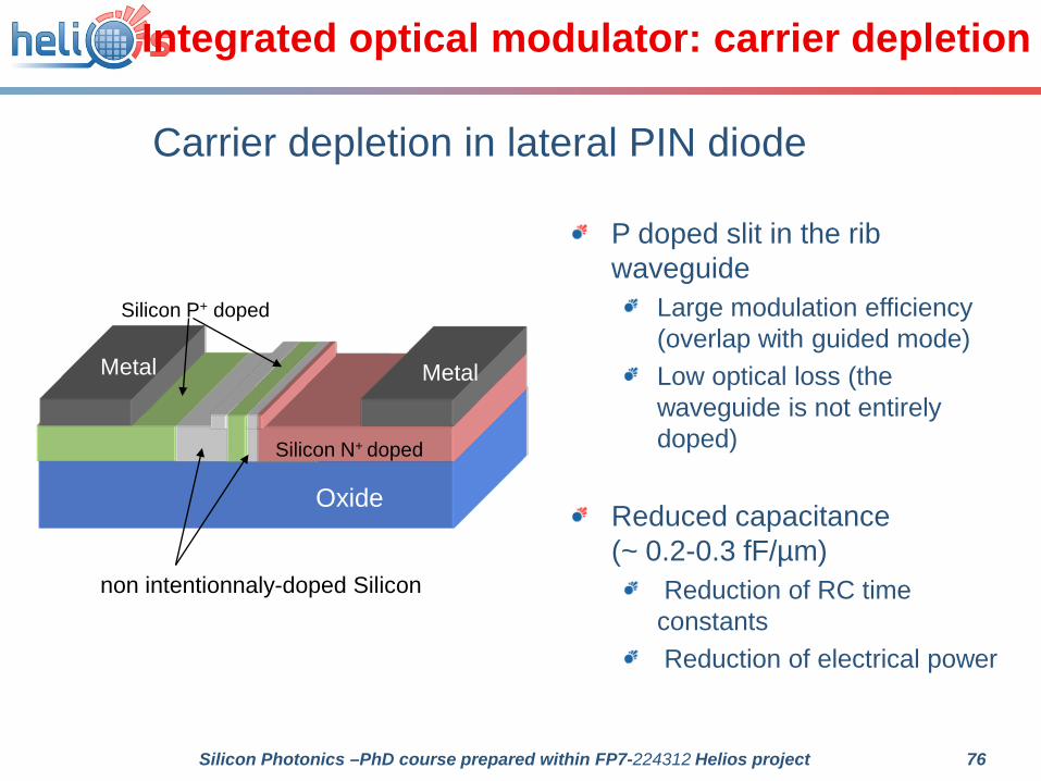
Integrated optical modulator: carrier depletion
non intentionnaly-doped Silicon
Oxide
Metal
Silicon P+ doped
Silicon N+ doped
Metal
Carrier depletion in lateral PIN diode
P doped slit in the rib waveguide
Large modulation efficiency (overlap with guided mode)Low optical loss (the waveguide is not entirely doped)
Reduced capacitance (~ 0.2-0.3 fF/µm)
Reduction of RC time constantsReduction of electrical power
77Silicon Photonics –PhD course prepared within FP7-224312 Helios project
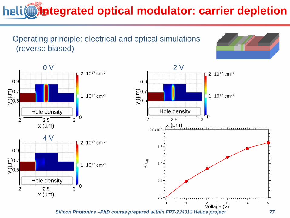
Integrated optical modulator: carrier depletion
Operating principle: electrical and optical simulations (reverse biased)
Hole density32.52
0.5
0.7
0.9
x (µm)
2 1017 cm-3
0
y (µ
m)
1 1017 cm-3
Hole density32.52
0.5
0.7
0.9
x (µm)
2 1017 cm-3
0
y (µ
m)
1 1017 cm-3
Hole density32.52
0.5
0.7
0.9
x (µm)
2 1017 cm-3
0
y (µ
m)
1 1017 cm-3
2.0x10⁻⁴
1.5
1.0
0.5
0.0
∆nef
f
543210Voltage (V)
0 V 2 V
4 V
78Silicon Photonics –PhD course prepared within FP7-224312 Helios project
Integrated optical modulator: carrier depletion
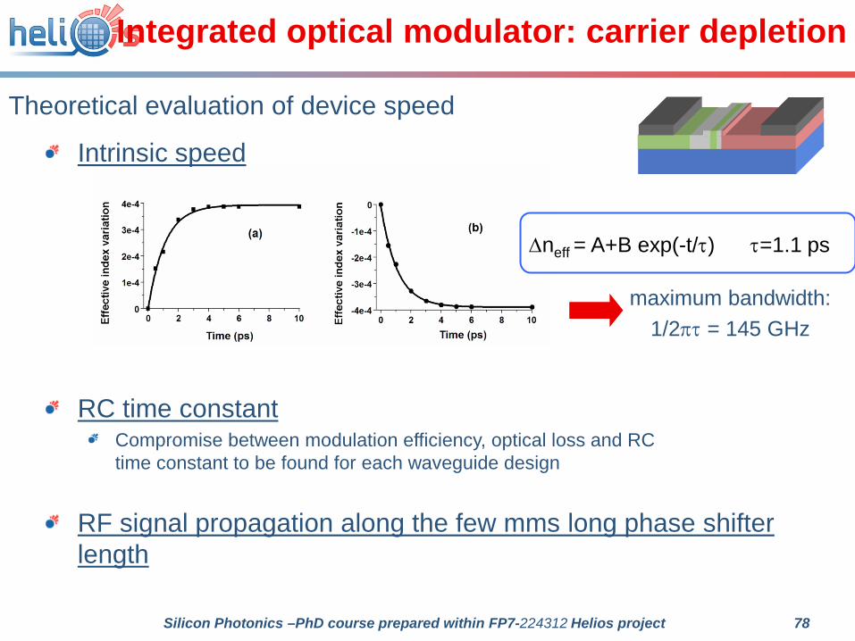
Theoretical evaluation of device speed
∆neff = A+B exp(-t/τ) τ=1.1 ps
maximum bandwidth: 1/2πτ = 145 GHz
RC time constantCompromise between modulation efficiency, optical loss and RC time constant to be found for each waveguide design
RF signal propagation along the few mms long phase shifter length
Intrinsic speed
79Silicon Photonics –PhD course prepared within FP7-224312 Helios project
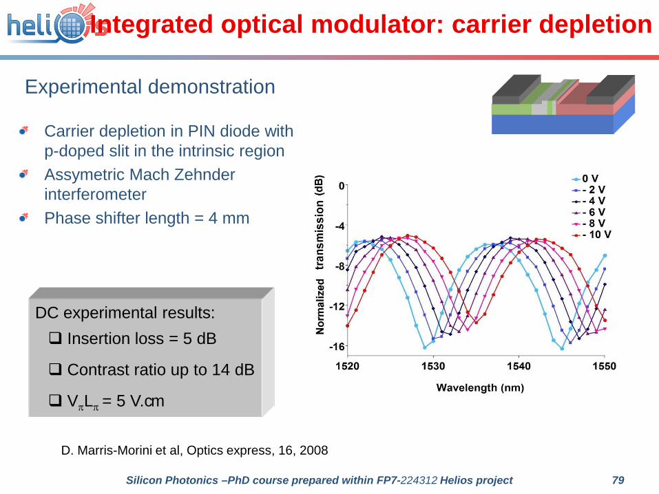
Integrated optical modulator: carrier depletion
D. Marris-Morini et al, Optics express, 16, 2008
Experimental demonstration
DC experimental results: Insertion loss = 5 dB
Contrast ratio up to 14 dB
VπLπ = 5 V.cm
Carrier depletion in PIN diode with p-doped slit in the intrinsic regionAssymetric Mach Zehnder interferometer Phase shifter length = 4 mm

80Silicon Photonics –PhD course prepared within FP7-224312 Helios project
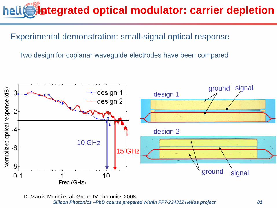
Integrated optical modulator: carrier depletion
RF experimental benches
81Silicon Photonics –PhD course prepared within FP7-224312 Helios project
Integrated optical modulator: carrier depletion
D. Marris-Morini et al, Group IV photonics 2008
10 GHz15 GHz
Experimental demonstration: small-signal optical response
Two design for coplanar waveguide electrodes have been compared
design 1
design 2
ground signal
ground signal
82Silicon Photonics –PhD course prepared within FP7-224312 Helios project
ConclusionIntensive research have been made in silicon photonics in the last years.
Silicon based optical modulator is one of the fundamental building blocs for high performance data transmission systems.
Optical modulation in/on silicon-based device has been proposed and demonstrated using a large number of physical effect:
• Electroabsorption using Franz-Keldysh and Quantun Confined Stark effects in SiGe and SiGe/Ge structures
• Electro-refraction in strained silicon and SiGe supperlattice
• Integration of III-V or polymer on silicon
• Free carrier concentration variations in silicon using carrier injection, accumulation, depletion, …

83Silicon Photonics –PhD course prepared within FP7-224312 Helios project
Conclusion
Numerous experimental demonstrations of optical modulator integrated in/on silicon waveguides have been made until the 1st
demonstration of GHz modulation 5 years ago.
Impressive progress in silicon modulators let’s hope that silicon based 10 and 40 Gbit/s data transmission systems will be available in the next years, for various applications (telecommunications, optical interconnect on microelectronics chips, core to core communications in microprocessors, etc…)

84Silicon Photonics –PhD course prepared within FP7-224312 Helios project
Acknowledgements
CEA - LETI (Grenoble, France)Jean Marc FEDELI
IEF (Orsay, France) Suzanne LAVAL Eric CASSAN Xavier LE ROUX Paul CROZAT Daniel PASCAL Sylvain MAINE Anatole LUPU David BOUVILLE Samson EDMOND Mathieu HALBWAX
French RMNT project (CAURICO)http://pages.ief.u-psud.fr/caurico/
IEF/MINERVE
CEA/LETIGrenoble, France
Clean rooms
Basic Technological Research
European Community's Seventh Framework Program (FP7)
“pHotonics ELectronics functional Integration on CMOS”
European Community's Sixth Framework Program (FP6)