Embed Size (px)
Citation preview
KSZ8041TL/FTL/MLL10BASE-T/100BASE-TX/100BASE-FX
Physical Layer Transceiver
Features
• Single-Chip 10BASE-T/100BASE-TX/100BASE-FX Physical Layer Solution
• Fully Compliant with IEEE 802.3u Standard
• Low Power CMOS Design, Power Consumption of <180 mW
• HP Auto MDI/MDI-X for Reliable Detection and Correction for Straight-Through and Crossover Cables with Disable and Enable Option
• Robust Operation Over Standard Cables
• LinkMD® TDR-Based Cable Diagnostics for Iden-tification of Faulty Copper Cabling
• Power Down and Power Saving Modes
• Fiber Support: 100BASE-FX (KSZ8041FTL Only)
• Back-to-Back Mode Support for 100 Mbps Repeater or Media Converter
• MII Interface Support
• RMII Interface Support with External 50 MHz Sys-tem Clock (KSZ8041TL/FTL Only)
• SMII Interface Support with External 125 MHz System Clock and 12.5 MHz Sync Clock from MAC (KSZ8041TL/FTL Only)
• MIIM (MDC/MDIO) Management Bus to 12.5 MHz for Rapid PHY Register Configuration
• Interrupt Pin Option
• Programmable LED Outputs for Link, Activity, and Speed
• Single Power Supply (3.3V)
• Built-in 1.8V Regulator for Core
• Available in 48-Pin LQFP (KSZ8041MLL) or 48-Pin TQFP (KSZ8041TL/FTL) Packages
Applications
• Printer
• LOM
• Game Console
• IPTV
• IP Phone
• IP Set-Top Box
• Media Converter
2017 Microchip Technology Inc. DS00002436B-page 1

KSZ8041TL/FTL/MLL
TO OUR VALUED CUSTOMERS
It is our intention to provide our valued customers with the best documentation possible to ensure successful use of your Microchipproducts. To this end, we will continue to improve our publications to better suit your needs. Our publications will be refined andenhanced as new volumes and updates are introduced.
If you have any questions or comments regarding this publication, please contact the Marketing Communications Department viaE-mail at [email protected]. We welcome your feedback.
Most Current Data SheetTo obtain the most up-to-date version of this data sheet, please register at our Worldwide Web site at:
http://www.microchip.com
You can determine the version of a data sheet by examining its literature number found on the bottom outside corner of any page. The last character of the literature number is the version number, (e.g., DS30000000A is version A of document DS30000000).
ErrataAn errata sheet, describing minor operational differences from the data sheet and recommended workarounds, may exist for cur-rent devices. As device/documentation issues become known to us, we will publish an errata sheet. The errata will specify therevision of silicon and revision of document to which it applies.
To determine if an errata sheet exists for a particular device, please check with one of the following:• Microchip’s Worldwide Web site; http://www.microchip.com• Your local Microchip sales office (see last page)
When contacting a sales office, please specify which device, revision of silicon and data sheet (include -literature number) you areusing.
Customer Notification SystemRegister on our web site at www.microchip.com to receive the most current information on all of our products.
DS00002436B-page 2 2017 Microchip Technology Inc.

2017 Microchip Technology Inc. DS00002436B-page 3
KSZ8041TL/FTL/MLL
Table of Contents
1.0 Introduction ..................................................................................................................................................................................... 42.0 Pin Description and Configuration .................................................................................................................................................. 63.0 Functional Description .................................................................................................................................................................. 194.0 Register Descriptions .................................................................................................................................................................... 355.0 Operational Characteristics ........................................................................................................................................................... 426.0 Electrical Characteristics ............................................................................................................................................................... 437.0 Timing Specifications .................................................................................................................................................................... 448.0 Selection of Isolation Transformers .............................................................................................................................................. 569.0 Package Outline ............................................................................................................................................................................ 57Appendix A: Data Sheet Revision History ........................................................................................................................................... 59The Microchip Web Site ...................................................................................................................................................................... 60Customer Change Notification Service ............................................................................................................................................... 60Customer Support ............................................................................................................................................................................... 60Product Identification System ............................................................................................................................................................. 61
KSZ8041TL/FTL/MLL
1.0 INTRODUCTION
1.1 General Description
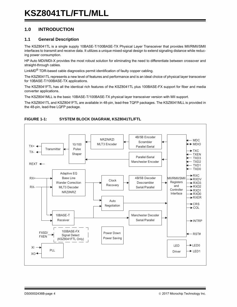
The KSZ8041TL is a single supply 10BASE-T/100BASE-TX Physical Layer Transceiver that provides MII/RMII/SMIIinterfaces to transmit and receive data. It utilizes a unique mixed-signal design to extend signaling distance while reduc-ing power consumption.
HP Auto MDI/MDI-X provides the most robust solution for eliminating the need to differentiate between crossover andstraight-through cables.
LinkMD® TDR-based cable diagnostics permit identification of faulty copper cabling.
The KSZ8041TL represents a new level of features and performance and is an ideal choice of physical layer transceiverfor 10BASE-T/100BASE-TX applications.
The KSZ8041FTL has all the identical rich features of the KSZ8041TL plus 100BASE-FX support for fiber and mediaconverter applications.
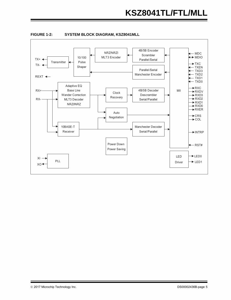
The KSZ8041MLL is the basic 10BASE-T/100BASE-TX physical layer transceiver version with MII support.
The KSZ8041TL and KSZ8041FTL are available in 48-pin, lead-free TQFP packages. The KSZ8041MLL is provided inthe 48-pin, lead-free LQFP package.
FIGURE 1-1: SYSTEM BLOCK DIAGRAM, KSZ8041TL/FTL
10/100Pulse
Shaper
NRZ/NRZIMLT3 Encoder
Parallel /SerialManchester Encoder
4B/5B EncoderScrambler
Parallel /SerialTransmitter
TX+
TX-
Adaptive EQBase Line
Wander CorrectionMLT3 Decoder
NRZI/NRZ
ClockRecovery
4B/5B DecoderDescrambler
Serial/Parallel
AutoNegotiation
10BASE-TReceiver
Manchester DecoderSerial/Parallel
PLLLED
Driver
MII/RMII/SMIIRegisters
andControllerInterface
RX-
RX+
XI
XOLED1
LED0
Power DownPower Saving
TXD3
TXD0TXD1TXD2
RXD3
TXENTXC
MDCMDIO
RXERRXD0RXD1RXD2
REXT
RXCRXDV
CRSCOL
RST#
INTRP
100BASE-FXSignal Detect
(KSZ8041FTL Only)
FXSD/FXEN
DS00002436B-page 4 2017 Microchip Technology Inc.
KSZ8041TL/FTL/MLL
FIGURE 1-2: SYSTEM BLOCK DIAGRAM, KSZ8041MLL
10/100Pulse
Shaper
NRZ/NRZIMLT3 Encoder
Parallel /SerialManchester Encoder
4B/5B EncoderScrambler
Parallel /SerialTransmitter
TX+
TX-
Adaptive EQBase Line
Wander CorrectionMLT3 Decoder
NRZI/NRZ
ClockRecovery
4B/5B DecoderDescrambler
Serial/Parallel
AutoNegotiation
10BASE-TReceiver
Manchester DecoderSerial/Parallel
PLLLED
Driver
MII
RX-
RX+
XI
XOLED1
LED0
Power DownPower Saving
TXD3
TXD0TXD1TXD2
RXD3
TXENTXC
MDCMDIO
RXERRXD0RXD1RXD2
REXT
RXCRXDV
CRSCOL
RST#
INTRP
2017 Microchip Technology Inc. DS00002436B-page 5

KSZ8041TL/FTL/MLL
2.0 PIN DESCRIPTION AND CONFIGURATION
FIGURE 2-1: KSZ8041TL 48-PIN TQFP ASSIGNMENT, (TOP VIEW)
1
NC
NC
TXC
RS
T#
INTRP
RE
XT
GN
D
RXER / RX_ER /ISO
GND
VDD_1.8
GND
GND
GND
GN
D
XO
VDDA_3.3
NC
TXD1 / TXD[1] / SYNC
TXD0 / TXD[0] / TX
TXEN /TX_EN
LED
1 /
SP
EE
D
LED
0 /
NW
AYE
N
CR
S /
CO
NFI
G1
NC
2
3
8
13 14 16 17
29
30
31
32
33
34
35
36
4142434445464748
RX+
TX-
RX-9
10
11
GN
D
24
TXD
3
TXD
2
GN
D
CO
L /
CO
NFI
G0
37383940
RXC
VDDIO_3.3
VDDIO_3.3
RXDV / CRSDV /CONFIG2
25
26
27
28
RX
D2
/ P
HY
AD
1
RX
D1
/ RXD
[1] /
P
HY
AD
2
RX
D0
/ RX
D[0
] / R
XD
UP
LEX
21 22 23
MD
IO
MD
C
RX
D3
/ P
HY
AD
0
18 19 20
XI /
RE
FCLK
/ C
LOC
K
15
TX+12
VDDA_1.8
VDDA_1.8
4
5
V1.8_OUT
VDDA_3.3
6
7
KSZ8041TL
DS00002436B-page 6 2017 Microchip Technology Inc.

KSZ8041TL/FTL/MLL
FIGURE 2-2: KSZ8041FTL 48-PIN TQFP ASSIGNMENT, (TOP VIEW)
1
NC
NC
TXC
RS
T#
INTRP
RE
XT
GN
D
RXER / RX_ER /ISO
GND
VDD_1.8
GND
GND
GND
GN
D
XO
VDDA_3.3
FXS
D /
FXE
N
TXD1 / TXD[1] / SYNC
TXD0 / TXD[0] / TX
TXEN /TX_EN
LED
1 /
SP
EE
D /
no F
EF
LED
0 /
NW
AYE
N
CR
S /
CO
NFI
G1
NC
2
3
8
13 14 16 17
29
30
31
32
33
34
35
36
4142434445464748
RX+
TX-
RX-9
10
11G
ND
24
TXD
3
TXD
2
GN
D
CO
L /
CO
NFI
G0
37383940
RXC
VDDIO_3.3
VDDIO_3.3
RXDV / CRSDV /CONFIG2
25
26
27
28
RX
D2
/ P
HY
AD
1
RX
D1
/ RXD
[1] /
P
HY
AD
2
RX
D0
/ RX
D[0
] / R
XD
UP
LEX
21 22 23
MD
IO
MD
C
RX
D3
/ P
HY
AD
0
18 19 20
XI /
RE
FCLK
/ C
LOC
K
15
TX+12
VDDA_1.8
VDDA_1.8
4
5
V1.8_OUT
VDDA_3.3
6
7
KSZ8041FTL
2017 Microchip Technology Inc. DS00002436B-page 7
KSZ8041TL/FTL/MLL
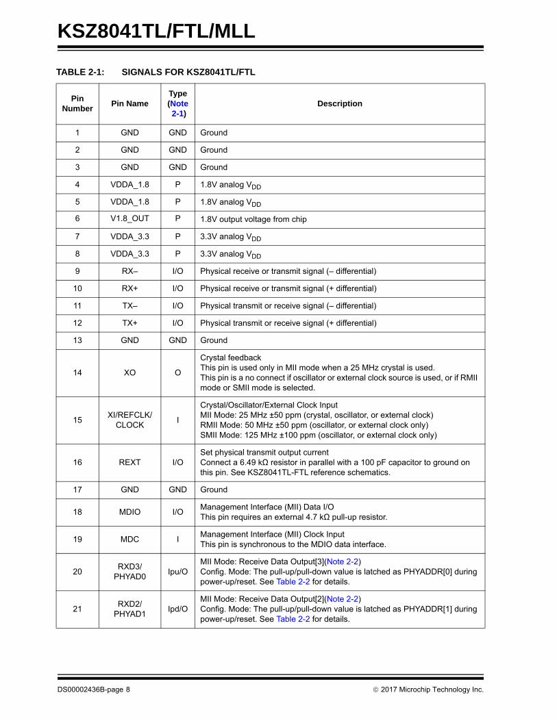
TABLE 2-1: SIGNALS FOR KSZ8041TL/FTL
Pin Number
Pin NameType (Note2-1)
Description
1 GND GND Ground
2 GND GND Ground
3 GND GND Ground
4 VDDA_1.8 P 1.8V analog VDD
5 VDDA_1.8 P 1.8V analog VDD
6 V1.8_OUT P 1.8V output voltage from chip
7 VDDA_3.3 P 3.3V analog VDD
8 VDDA_3.3 P 3.3V analog VDD
9 RX– I/O Physical receive or transmit signal (– differential)
10 RX+ I/O Physical receive or transmit signal (+ differential)
11 TX– I/O Physical transmit or receive signal (– differential)
12 TX+ I/O Physical transmit or receive signal (+ differential)
13 GND GND Ground
14 XO O
Crystal feedbackThis pin is used only in MII mode when a 25 MHz crystal is used.This pin is a no connect if oscillator or external clock source is used, or if RMII mode or SMII mode is selected.
15XI/REFCLK/
CLOCKI
Crystal/Oscillator/External Clock InputMII Mode: 25 MHz ±50 ppm (crystal, oscillator, or external clock)RMII Mode: 50 MHz ±50 ppm (oscillator, or external clock only)SMII Mode: 125 MHz ±100 ppm (oscillator, or external clock only)
16 REXT I/OSet physical transmit output currentConnect a 6.49 kΩ resistor in parallel with a 100 pF capacitor to ground on this pin. See KSZ8041TL-FTL reference schematics.
17 GND GND Ground
18 MDIO I/OManagement Interface (MII) Data I/OThis pin requires an external 4.7 kΩ pull-up resistor.
19 MDC IManagement Interface (MII) Clock InputThis pin is synchronous to the MDIO data interface.
20RXD3/
PHYAD0Ipu/O
MII Mode: Receive Data Output[3](Note 2-2) Config. Mode: The pull-up/pull-down value is latched as PHYADDR[0] during power-up/reset. See Table 2-2 for details.
21RXD2/
PHYAD1Ipd/O
MII Mode: Receive Data Output[2](Note 2-2) Config. Mode: The pull-up/pull-down value is latched as PHYADDR[1] during power-up/reset. See Table 2-2 for details.
DS00002436B-page 8 2017 Microchip Technology Inc.
KSZ8041TL/FTL/MLL
22RXD1/RXD[1]/PHYAD2
Ipd/O
MII Mode: Receive Data Output[1](Note 2-2) RMII Mode: Receive Data Output[1](Note 2-3) Config. Mode: The pull-up/pull-down value is latched as PHYADDR[2] during power-up/reset. See Table 2-2 for details.
23
RXD0/RXD[0]/
RXDUPLEX
Ipu/O
MII Mode: Receive Data Output[0](Note 2-2) RMII Mode: Receive Data Output[0](Note 2-3) SMII Mode: Receive Data and Control(Note 2-4) Config. Mode: Latched as DUPLEX (register 0h, bit 8) during power-up/reset. See Table 2-2 for details.
24 GND GND Ground
25 VDDIO_3.3 P 3.3V digital VDD
26 VDDIO_3.3 P 3.3V digital VDD
27RXDV/
CRSDV/CONFIG2
Ipd/O
MII Mode: Receive Data Valid Output RMII Mode: Carrier Sense/Receive Data Valid Output Config. Mode: The pull-up/pull-down value is latched as CONFIG2 during power-up/reset. See Table 2-2 for details.
28 RXC O MII Mode: Receive Clock Output.
29RXER/
RX_ER/ISO
Ipd/O
MII Mode: Receive Error Output RMII Mode: Receive Error Output Config. Mode: The pull-up/pull-down value is latched as ISOLATE during power-up/reset. See Table 2-2 for details.
30 GND GND Ground
31 VDD_1.8 P 1.8V digital VDD
32 INTRP Opu
Interrupt Output: Programmable Interrupt OutputRegister 1Bh is the Interrupt Control/Status Register for programming the interrupt conditions and reading the interrupt status. Register 1Fh bit 9 sets the interrupt output to active-low (default) or active-high.
33 TXC I/OMII Mode: Transmit Clock OutputMII Back-to-Back Mode: Transmit Clock Input
34TXEN/TX_EN
IMII Mode: Transmit Enable Input RMII Mode: Transmit Enable Input
35TXD0/
TXD[0]/TX
IMII Mode: Transmit Data Input[0](Note 2-5) RMII Mode: Transmit Data Input[0](Note 2-6) SMII Mode: Transmit Data and Control(Note 2-7)
36TXD1/
TXD[1]/SYNC
IMII Mode: Transmit Data Input[1](Note 2-5) RMII Mode: Transmit Data Input[1](Note 2-6) SMII Mode: SYNC Clock Input
37 GND GND Ground
38 TXD2 I MII Mode: Transmit Data Input[2](Note 2-5)
39 TXD3 I MII Mode: Transmit Data Input[3](Note 2-5)
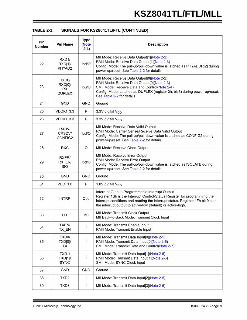
TABLE 2-1: SIGNALS FOR KSZ8041TL/FTL (CONTINUED)
Pin Number
Pin NameType (Note2-1)
Description
2017 Microchip Technology Inc. DS00002436B-page 9
KSZ8041TL/FTL/MLL
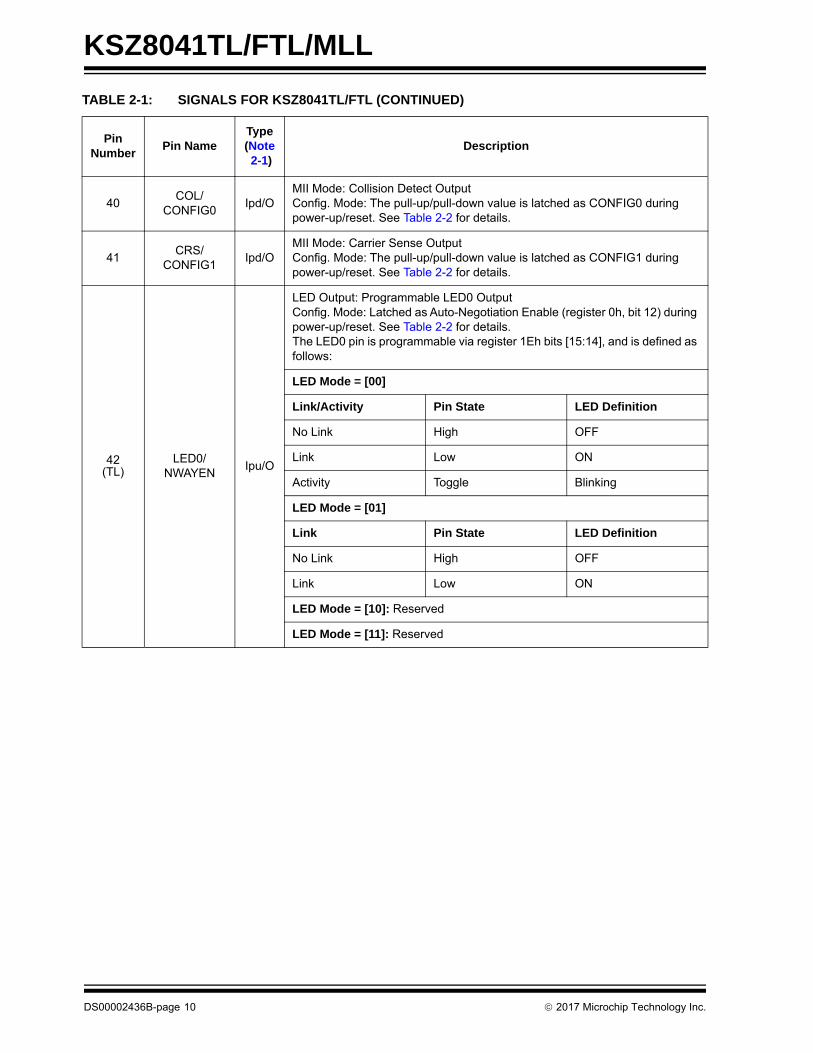
40COL/
CONFIG0Ipd/O
MII Mode: Collision Detect Output Config. Mode: The pull-up/pull-down value is latched as CONFIG0 during power-up/reset. See Table 2-2 for details.
41CRS/
CONFIG1Ipd/O
MII Mode: Carrier Sense Output Config. Mode: The pull-up/pull-down value is latched as CONFIG1 during power-up/reset. See Table 2-2 for details.
42(TL)
LED0/NWAYEN
Ipu/O
LED Output: Programmable LED0 Output Config. Mode: Latched as Auto-Negotiation Enable (register 0h, bit 12) during power-up/reset. See Table 2-2 for details.The LED0 pin is programmable via register 1Eh bits [15:14], and is defined as follows:
LED Mode = [00]
Link/Activity Pin State LED Definition
No Link High OFF
Link Low ON
Activity Toggle Blinking
LED Mode = [01]
Link Pin State LED Definition
No Link High OFF
Link Low ON
LED Mode = [10]: Reserved
LED Mode = [11]: Reserved
TABLE 2-1: SIGNALS FOR KSZ8041TL/FTL (CONTINUED)
Pin Number
Pin NameType (Note2-1)
Description
DS00002436B-page 10 2017 Microchip Technology Inc.
KSZ8041TL/FTL/MLL
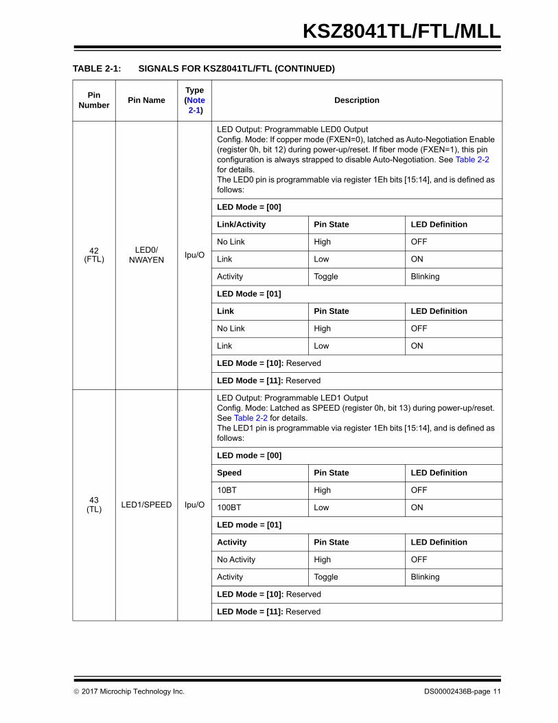
42(FTL)
LED0/NWAYEN
Ipu/O
LED Output: Programmable LED0 Output Config. Mode: If copper mode (FXEN=0), latched as Auto-Negotiation Enable (register 0h, bit 12) during power-up/reset. If fiber mode (FXEN=1), this pin configuration is always strapped to disable Auto-Negotiation. See Table 2-2 for details.The LED0 pin is programmable via register 1Eh bits [15:14], and is defined as follows:
LED Mode = [00]
Link/Activity Pin State LED Definition
No Link High OFF
Link Low ON
Activity Toggle Blinking
LED Mode = [01]
Link Pin State LED Definition
No Link High OFF
Link Low ON
LED Mode = [10]: Reserved
LED Mode = [11]: Reserved
43(TL) LED1/SPEED Ipu/O
LED Output: Programmable LED1 Output Config. Mode: Latched as SPEED (register 0h, bit 13) during power-up/reset. See Table 2-2 for details.The LED1 pin is programmable via register 1Eh bits [15:14], and is defined as follows:
LED mode = [00]
Speed Pin State LED Definition
10BT High OFF
100BT Low ON
LED mode = [01]
Activity Pin State LED Definition
No Activity High OFF
Activity Toggle Blinking
LED Mode = [10]: Reserved
LED Mode = [11]: Reserved
TABLE 2-1: SIGNALS FOR KSZ8041TL/FTL (CONTINUED)
Pin Number
Pin NameType (Note2-1)
Description
2017 Microchip Technology Inc. DS00002436B-page 11

KSZ8041TL/FTL/MLL
Note 2-1 P = power supplyGND = groundI = inputO = outputI/O = bi-directionalIpu/O = Input with internal pull-up (40 kΩ ±30%) during power-up/reset; output pin otherwise.Ipd/O = Input with internal pull-down (40 kΩ ±30%) during power-up/reset; output pin otherwise.Ipu = Input with internal pull-up. (40 kΩ ±30%)Ipd = Input with internal pull-down. (40 kΩ ±30%)Opu = Output with internal pull-up. (40 kΩ ±30%)
Note 2-2 MII Rx Mode: The RXD[3..0] bits are synchronous with RXCLK. When RXDV is asserted, RXD[3..0]presents valid data to MAC through the MII. RXD[3..0] is invalid when RXDV is de-asserted.
Note 2-3 RMII Rx Mode: The RXD[1:0] bits are synchronous with REF_CLK. For each clock period in whichCRS_DV is asserted, two bits of recovered data are sent from the PHY.
43(FTL)
LED1/SPEEDno FEF
Ipu/O
LED Output: Programmable LED1 Output Config. Mode: If copper mode (FXEN=0), latched as SPEED (register 0h, bit 13) during power-up/reset. If fiber mode (FXEN=1), latched as no FEF (no Far-End Fault) during power-up/reset. See Table 2-2 for details.The LED1 pin is programmable via register 1Eh bits [15:14], and is defined as follows:
LED mode = [00]
Speed Pin State LED Definition
10BT High OFF
100BT Low ON
LED mode = [01]
Activity Pin State LED Definition
No Activity High OFF
Activity Toggle Blinking
LED Mode = [10]: Reserved
LED Mode = [11]: Reserved
44 NC — No connect
45 NC — No connect
46 NC — No connect
47 RST# I Chip reset (active-low)
48(TL) NC — No connect
48(FTL) FXSD/FXEN Ipd
FXSD: Signal Detect for 100BASE-FX fiber modeFXEN: Fiber Enable for 100BASE-FX fiber modeIf FXEN=0, fiber mode is disabled. PHY is in copper mode. The default is “0”. See “100BASE-FX Operation” section for details.
TABLE 2-1: SIGNALS FOR KSZ8041TL/FTL (CONTINUED)
Pin Number
Pin NameType (Note2-1)
Description
DS00002436B-page 12 2017 Microchip Technology Inc.
KSZ8041TL/FTL/MLL
Note 2-4 SMII Rx Mode: Receive data and control information are sent in 10 bit segments. In 100 MBit mode,each segment represents a new byte of data. In 10 MBit mode, each segment is repeated ten times;therefore, every ten segments represent a new byte of data. The MAC can sample any one of every10 segments in 10 MBit mode.
Note 2-5 MII Tx Mode: The TXD[3..0] bits are synchronous with TXCLK. When TXEN is asserted, TXD[3..0]presents valid data from the MAC through the MII. TXD[3..0] has no effect when TXEN is de-asserted.
Note 2-6 RMII Tx Mode: The TXD[1:0] bits are synchronous with REF_CLK. For each clock period in whichTX_EN is asserted, two bits of data are received by the PHY from the MAC.
Note 2-7 SMII Tx Mode: Transmit data and control information are received in 10 bit segments. In 100 MBitmode, each segment represents a new byte of data. In 10 MBit mode, each segment is repeated tentimes; therefore, every ten segments represent a new byte of data. The PHY can sample any one ofevery 10 segments in 10 MBit mode.
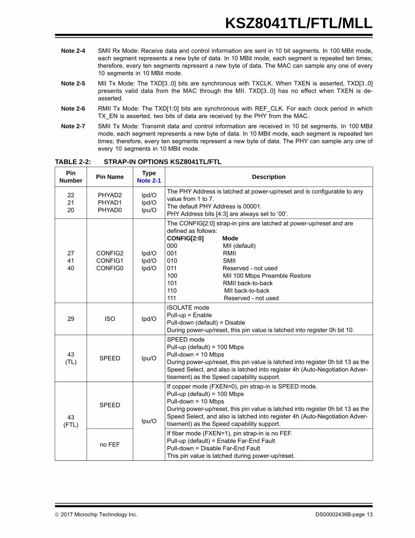
TABLE 2-2: STRAP-IN OPTIONS KSZ8041TL/FTL
Pin Number
Pin NameType
Note 2-1Description
222120
PHYAD2PHYAD1PHYAD0
Ipd/OIpd/OIpu/O
The PHY Address is latched at power-up/reset and is configurable to any value from 1 to 7.The default PHY Address is 00001.PHY Address bits [4:3] are always set to ‘00’.
274140
CONFIG2CONFIG1CONFIG0
Ipd/OIpd/OIpd/O
The CONFIG[2:0] strap-in pins are latched at power-up/reset and are defined as follows:CONFIG[2:0] Mode000 MII (default)001 RMII010 SMII011 Reserved - not used100 MII 100 Mbps Preamble Restore101 RMII back-to-back110 MII back-to-back111 Reserved - not used
29 ISO Ipd/O
ISOLATE modePull-up = EnablePull-down (default) = DisableDuring power-up/reset, this pin value is latched into register 0h bit 10.
43(TL)
SPEED Ipu/O
SPEED modePull-up (default) = 100 MbpsPull-down = 10 MbpsDuring power-up/reset, this pin value is latched into register 0h bit 13 as the Speed Select, and also is latched into register 4h (Auto-Negotiation Adver-tisement) as the Speed capability support.
43(FTL)
SPEED
Ipu/O
If copper mode (FXEN=0), pin strap-in is SPEED mode.Pull-up (default) = 100 MbpsPull-down = 10 MbpsDuring power-up/reset, this pin value is latched into register 0h bit 13 as the Speed Select, and also is latched into register 4h (Auto-Negotiation Adver-tisement) as the Speed capability support.
no FEF
If fiber mode (FXEN=1), pin strap-in is no FEF.Pull-up (default) = Enable Far-End FaultPull-down = Disable Far-End FaultThis pin value is latched during power-up/reset.
2017 Microchip Technology Inc. DS00002436B-page 13

KSZ8041TL/FTL/MLL
Note 2-1 Ipu/O = Input with internal pull-up (40 kΩ ±30%) during power-up/reset; output pin otherwise.Ipd/O = Input with internal pull-down (40 kΩ ±30%) during power-up/reset; output pin otherwise.
Pin strap-ins are latched during power-up or reset. In some systems, the MAC receive input pins may drive high duringpower-up or reset, and consequently cause the PHY strap-in pins on the MII/RMII/SMII signals to be latched high. Inthis case, it is recommended to add 1 kΩ pull-downs on these PHY strap-in pins to ensure the PHY does not strap-in toISOLATE mode, or is not configured with an incorrect PHY Address.
23 DUPLEX Ipu/O
DUPLEX modePull-up (default) = Half-DuplexPull-down = Full-DuplexDuring power-up/reset, this pin value is latched into register 0h bit 8 as the Duplex Mode.
42(TL)
NWAYEN Ipu/O
Nway Auto-Negotiation EnablePull-up (default) = Enable Auto-NegotiationPull-down = Disable Auto-NegotiationDuring power-up/reset, this pin value is latched into register 0h bit 12.
42(FTL)
NWAYEN Ipu/O
If copper mode (FXEN=0), pin strap-in is Nway Auto-Negotiation Enable.Pull-up (default) = Enable Auto-NegotiationPull-down = Disable Auto-NegotiationDuring power-up/reset, this pin value is latched into register 0h bit 12.
If fiber mode (FXEN=1), this pin configuration is always strapped to disable Auto-Negotiation.
TABLE 2-2: STRAP-IN OPTIONS KSZ8041TL/FTL (CONTINUED)
Pin Number
Pin NameType
Note 2-1Description
DS00002436B-page 14 2017 Microchip Technology Inc.
KSZ8041TL/FTL/MLL
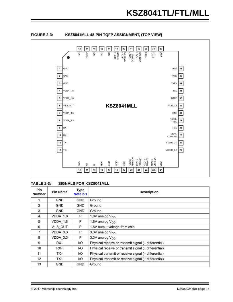
FIGURE 2-3: KSZ8041MLL 48-PIN TQFP ASSIGNMENT, (TOP VIEW)
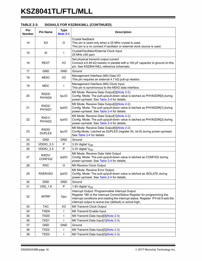
TABLE 2-3: SIGNALS FOR KSZ8041MLL
Pin Number
Pin NameType
Note 2-1Description
1 GND GND Ground
2 GND GND Ground
3 GND GND Ground
4 VDDA_1.8 P 1.8V analog VDD
5 VDDA_1.8 P 1.8V analog VDD
6 V1.8_OUT P 1.8V output voltage from chip
7 VDDA_3.3 P 3.3V analog VDD
8 VDDA_3.3 P 3.3V analog VDD
9 RX– I/O Physical receive or transmit signal (– differential)
10 RX+ I/O Physical receive or transmit signal (+ differential)
11 TX– I/O Physical transmit or receive signal (– differential)
12 TX+ I/O Physical transmit or receive signal (+ differential)
13 GND GND Ground
1
NC
NC
TXC
RST
#
INTRPR
EXT
GN
D
RXER /ISO
GND
VDD_1.8
GND
GND
GND
GN
D
XO
VDDA_3.3
NC
TXD1
TXD0
TXEN
LED
1 /
SPEE
D
LED
0 /
NW
AYEN
CR
S /
CO
NFI
G1
NC
2
3
8
13 14 16 17
29
30
31
32
33
34
35
36
4142434445464748
RX+
TX-
RX-9
10
11
GN
D
24
TXD
3
TXD
2
GN
D
CO
L /
CO
NFI
G0
37383940
RXC
VDDIO_3.3
VDDIO_3.3
RXDV /CONFIG2
25
26
27
28
RX
D2
/ PH
YAD
1
RX
D1
/ PH
YAD
2
RXD
0 /
DU
PLEX
21 22 23
MD
IO
MD
C
RX
D3
/ PH
YAD
0
18 19 20
XI
15
TX+12
VDDA_1.8
VDDA_1.8
4
5
V1.8_OUT
VDDA_3.3
6
7
KSZ8041MLL
2017 Microchip Technology Inc. DS00002436B-page 15
KSZ8041TL/FTL/MLL
14 XO OCrystal feedbackThis pin is used only when a 25 MHz crystal is used.This pin is a no connect if oscillator or external clock source is used.
15 XI ICrystal/Oscillator/External Clock Input25 MHz ±50 ppm
16 REXT I/OSet physical transmit output currentConnect a 6.49 kΩ resistor in parallel with a 100 pF capacitor to ground on this pin. See KSZ8041MLL reference schematic.
17 GND GND Ground
18 MDIO I/OManagement Interface (MII) Data I/OThis pin requires an external 4.7 kΩ pull-up resistor.
19 MDC IManagement Interface (MII) Clock InputThis pin is synchronous to the MDIO data interface.
20RXD3/
PHYAD0Ipu/O
MII Mode: Receive Data Output[3](Note 2-2) Config. Mode: The pull-up/pull-down value is latched as PHYADDR[0] during power-up/reset. See Table 2-4 for details.
21RXD2/
PHYAD1Ipd/O
MII Mode: Receive Data Output[2](Note 2-2) Config. Mode: The pull-up/pull-down value is latched as PHYADDR[1] during power-up/reset. See Table 2-4 for details.
22RXD1/
PHYAD2Ipd/O
MII Mode: Receive Data Output[1](Note 2-2) Config. Mode: The pull-up/pull-down value is latched as PHYADDR[2] during power-up/reset. See Table 2-4 for details.
23RXD0/
DUPLEXIpu/O
MII Mode: Receive Data Output[0](Note 2-2) Config Mode: Latched as DUPLEX (register 0h, bit 8) during power-up/reset. See Table 2-4 for details.
24 GND GND Ground
25 VDDIO_3.3 P 3.3V digital VDD
26 VDDIO_3.3 P 3.3V digital VDD
27RXDV/
CONFIG2Ipd/O
MII Mode: Receive Data Valid Output Config. Mode: The pull-up/pull-down value is latched as CONFIG2 during power-up/reset. See Table 2-4 for details.
28 RXC O MII Receive Clock Output
29 RXER/ISO Ipd/OMII Mode: Receive Error Output Config. Mode: The pull-up/pull-down value is latched as ISOLATE during power-up/reset. See Table 2-4 for details.
30 GND GND Ground
31 VDD_1.8 P 1.8V digital VDD
32 INTRP Opu
Interrupt Output: Programmable Interrupt OutputRegister 1Bh is the Interrupt Control/Status Register for programming the interrupt conditions and reading the interrupt status. Register 1Fh bit 9 sets the interrupt output to active-low (default) or active-high.
33 TXC I/O MII Transmit Clock Output
34 TXEN I MII Transmit Enable Input
35 TXD0 I MII Transmit Data Input[0](Note 2-3)
36 TXD1 I MII Transmit Data Input[1](Note 2-3)
37 GND GND Ground
38 TXD2 I MII Transmit Data Input[2](Note 2-3)
39 TXD3 I MII Transmit Data Input[3](Note 2-3)
TABLE 2-3: SIGNALS FOR KSZ8041MLL (CONTINUED)
Pin Number
Pin NameType
Note 2-1Description
DS00002436B-page 16 2017 Microchip Technology Inc.
KSZ8041TL/FTL/MLL
Note 2-1 P = power supplyGND = groundI = inputO = outputI/O = bi-directional
40COL/
CONFIG0Ipd/O
MII Mode: Collision Detect Output Config. Mode: The pull-up/pull-down value is latched as CONFIG0 during power-up/reset. See Table 2-4 for details.
41CRS/
CONFIG1Ipd/O
MII Mode: Carrier Sense Output Config. Mode: The pull-up/pull-down value is latched as CONFIG1 during power-up/reset. See Table 2-4 for details.
42LED0/
NWAYENIpu/O
LED Output: Programmable LED0 Output Config. Mode: Latched as Auto-Negotiation Enable (register 0h, bit 12) during power-up/reset. See Table 2-4 for details.The LED0 pin is programmable via register 1Eh bits [15:14], and is defined as follows:
LED Mode = [00]
Link/Activity Pin State LED Definition
No Link High OFF
Link Low ON
Activity Toggle Blinking
LED Mode = [01]
Link Pin State LED Definition
No Link High OFF
Link Low ON
LED Mode = [10]: Reserved
LED Mode = [11]: Reserved
43LED1/
SPEEDIpu/O
LED Output: Programmable LED1 Output Config. Mode: Latched as SPEED (register 0h, bit 13) during power-up/reset. See Table 2-4 for details.The LED1 pin is programmable via register 1Eh bits [15:14], and is defined as follows:
LED Mode = [00]
Speed Pin State LED Definition
10BT High OFF
100BT Low ON
LED Mode = [01]
Activity Pin State LED Definition
No Activity High OFF
Activity Toggle Blinking
LED Mode = [10]: Reserved
LED Mode = [11]: Reserved
44 NC — No connect
45 NC — No connect
46 NC — No connect
47 RST# I Chip reset (active-low)
48 NC — No connect
TABLE 2-3: SIGNALS FOR KSZ8041MLL (CONTINUED)
Pin Number
Pin NameType
Note 2-1Description
2017 Microchip Technology Inc. DS00002436B-page 17
KSZ8041TL/FTL/MLL
Ipu/O = Input with internal pull-up (40 kΩ ±30%) during power-up/reset; output pin otherwise.Ipd/O = Input with internal pull-down (40 kΩ ±30%) during power-up/reset; output pin otherwise.Ipu = Input with internal pull-up. (40 kΩ ±30%)Ipd = Input with internal pull-down. (40 kΩ ±30%)Opu = Output with internal pull-up. (40 kΩ ±30%)
Note 2-2 MII Rx Mode: The RXD[3..0] bits are synchronous with RXCLK. When RXDV is asserted, RXD[3..0]presents valid data to MAC through the MII. RXD[3..0] is invalid when RXDV is de-asserted.
Note 2-3 MII Tx Mode: The TXD[3..0] bits are synchronous with TXCLK. When TXEN is asserted, TXD[3..0]presents valid data from the MAC through the MII. TXD[3..0] has no effect when TXEN is de-asserted.
Note 2-1 Ipu/O = Input with internal pull-up (40 kΩ ±30%) during power-up/reset; output pin otherwise.Ipd/O = Input with internal pull-down (40 kΩ ±30%) during power-up/reset; output pin otherwise.
Pin strap-ins are latched during power-up or reset. In some systems, the MAC receive input pins may drive high duringpower-up or reset, and consequently cause the PHY strap-in pins on the MII signals to be latched high. In this case, itis recommended to add 1 kΩ pull-downs on these PHY strap-in pins to ensure the PHY does not strap-in to ISOLATEmode, or is not configured with an incorrect PHY Address.
TABLE 2-4: STRAP-IN OPTIONS KSZ8041MLL
Pin Number
Pin NameType
Note 2-1Description
222120
PHYAD2PHYAD1PHYAD0
Ipd/OIpd/OIpu/O
The PHY Address is latched at power-up / reset and is configurable to any value from 1 to 7.The default PHY Address is 00001.PHY Address bits [4:3] are always set to ‘00’.
274140
CONFIG2CONFIG1CONFIG0
Ipd/OIpd/OIpd/O
The CONFIG[2:0] strap-in pins are latched at power-up / reset and are defined as follows:
CONFIG[2:0] Mode000 MII (default)001 Reserved - not used010 Reserved - not used011 Reserved - not used100 MII 100 Mbps Preamble Restore101 Reserved - not used110 MII Back-to-Back111 Reserved - not used
29 ISO Ipd/O
ISOLATE modePull-up = EnablePull-down (default) = DisableDuring power-up/reset, this pin value is latched into register 0h bit 10.
43 SPEED Ipu/O
SPEED modePull-up (default) = 100 MbpsPull-down = 10 MbpsDuring power-up/reset, this pin value is latched into register 0h bit 13 as the Speed Select, and also is latched into register 4h (Auto-Negotiation Advertise-ment) as the Speed capability support.
23 DUPLEX Ipu/O
DUPLEX modePull-up (default) = Half-DuplexPull-down = Full-DuplexDuring power-up/reset, this pin value is latched into register 0h bit 8 as the Duplex Mode.
42 NWAYEN Ipu/O
Nway Auto-Negotiation EnablePull-up (default) = Enable Auto-NegotiationPull-down = Disable Auto-NegotiationDuring power-up/reset, this pin value is latched into register 0h bit 12.
DS00002436B-page 18 2017 Microchip Technology Inc.

KSZ8041TL/FTL/MLL
3.0 FUNCTIONAL DESCRIPTION
The KSZ8041TL is a single 3.3V supply Fast Ethernet transceiver. It is fully compliant with the IEEE 802.3u specifica-tion.
On the media side, the KSZ8041TL supports 10BASE-T and 100BASE-TX with HP auto MDI/MDI-X for reliable detec-tion of and correction for straight-through and crossover cables.
The KSZ8041TL offers a choice of MII, RMII, or SMII data interface connection to a MAC processor. The MII manage-ment bus option gives the MAC processor complete access to the KSZ8041TL control and status registers. Additionally,an interrupt pin eliminates the need for the processor to poll for PHY status change.
Physical signal transmission and reception are enhanced through the use of patented analog circuitries that make thedesign more efficient and allow for lower power consumption and smaller chip die size.
The KSZ8041FTL has all the identical rich features of the KSZ8041TL plus 100BASE-FX fiber support.
The KSZ8041MLL is the basic 10BASE-T/100BASE-TX copper version with MII support.
3.1 100BASE-TX Transmit
The 100BASE-TX transmit function performs parallel-to-serial conversion, 4B/5B coding, scrambling, NRZ-to-NRZI con-version, and MLT3 encoding and transmission.
The circuitry starts with a parallel-to-serial conversion, which converts the MII data from the MAC into a 125 MHz serialbit stream. The data and control stream is then converted into 4B/5B coding, followed by a scrambler. The serializeddata is further converted from NRZ-to-NRZI format, and then transmitted in MLT3 current output.
The output current is set by an external 6.49 kΩ 1% resistor for the 1:1 transformer ratio. It has typical rise/fall times of4 ns and complies with the ANSI TP-PMD standard regarding amplitude balance, overshoot and timing jitter. The wave-shaped 10BASE-T output drivers are also incorporated into the 100BASE-TX drivers.
3.2 100BASE-TX Receive
The 100BASE-TX receiver function performs adaptive equalization, DC restoration, MLT3-to-NRZI conversion, data andclock recovery, NRZI-to-NRZ conversion, de-scrambling, 4B/5B decoding, and serial-to-parallel conversion.
The receiving side starts with the equalization filter to compensate for inter-symbol interference (ISI) over the twistedpair cable. Since the amplitude loss and phase distortion is a function of the cable length, the equalizer must adjust itscharacteristics to optimize performance. In this design, the variable equalizer makes an initial estimation based uponcomparisons of incoming signal strength against some known cable characteristics, and then tunes itself for optimiza-tion. This is an ongoing process and self-adjusts against environmental changes such as temperature variations.
Next, the equalized signal goes through a DC restoration and data conversion block. The DC restoration circuit is usedto compensate for the effect of baseline wander and to improve the dynamic range. The differential data conversioncircuit converts the MLT3 format back to NRZI. The slicing threshold is also adaptive.
The clock recovery circuit extracts the 125 MHz clock from the edges of the NRZI signal. This recovered clock is thenused to convert the NRZI signal into the NRZ format. This signal is sent through the de-scrambler followed by the 4B/5B decoder. Finally, the NRZ serial data is converted to the MII format and provided as the input data to the MAC.
3.3 PLL Clock Synthesizer
The KSZ8041TL/FTL/MLL generates 125 MHz, 25 MHz, and 20 MHz clocks for system timing. In MII mode, internalclocks are generated from an external 25 MHz crystal or oscillator. For the KSZ8041TL/FTL, in RMII and SMII modes,these internal clocks are generated from external 50 MHz and 125 MHz oscillators or system clocks, respectively.
3.4 Scrambler/De-scrambler (100BASE-TX Only)
The purpose of the scrambler is to spread the power spectrum of the signal in order to reduce EMI and baseline wander.
3.5 10BASE-T Transmit
The 10BASE-T drivers are incorporated with the 100BASE-TX drivers to allow for transmission using the same mag-netic. The drivers also perform internal wave-shaping and pre-emphasize, and output 10BASE-T signals with a typicalamplitude of 2.5V peak. The 10BASE-T signals have harmonic contents that are at least 27 dB below the fundamentalfrequency when driven by an all-ones Manchester-encoded signal.
2017 Microchip Technology Inc. DS00002436B-page 19
KSZ8041TL/FTL/MLL
3.6 10BASE-T Receive
On the receive side, input buffer and level detecting squelch circuits are employed. A differential input receiver circuitand a PLL performs the decoding function. The Manchester-encoded data stream is separated into clock signal andNRZ data. A squelch circuit rejects signals with levels less than 400 mV or with short pulse widths to prevent noise atthe RX+ and RX– inputs from falsely trigger the decoder. When the input exceeds the squelch limit, the PLL locks ontothe incoming signal and the KSZ8041TL/FTL/MLL decodes a data frame. The receive clock is kept active during idleperiods in between data reception.
3.7 SQE and Jabber Function (10BASE-T Only)
In 10BASE-T operation, a short pulse is put out on the COL pin after each frame is transmitted. This SQE Test is requiredas a test of the 10BASE-T transmit/receive path. If transmit enable (TXEN) is high for more than 20 ms (jabbering), the10BASE-T transmitter is disabled and COL is asserted high. If TXEN is then driven low for more than 250 ms, the10BASE-T transmitter is re-enabled and COL is de-asserted (returns to low).
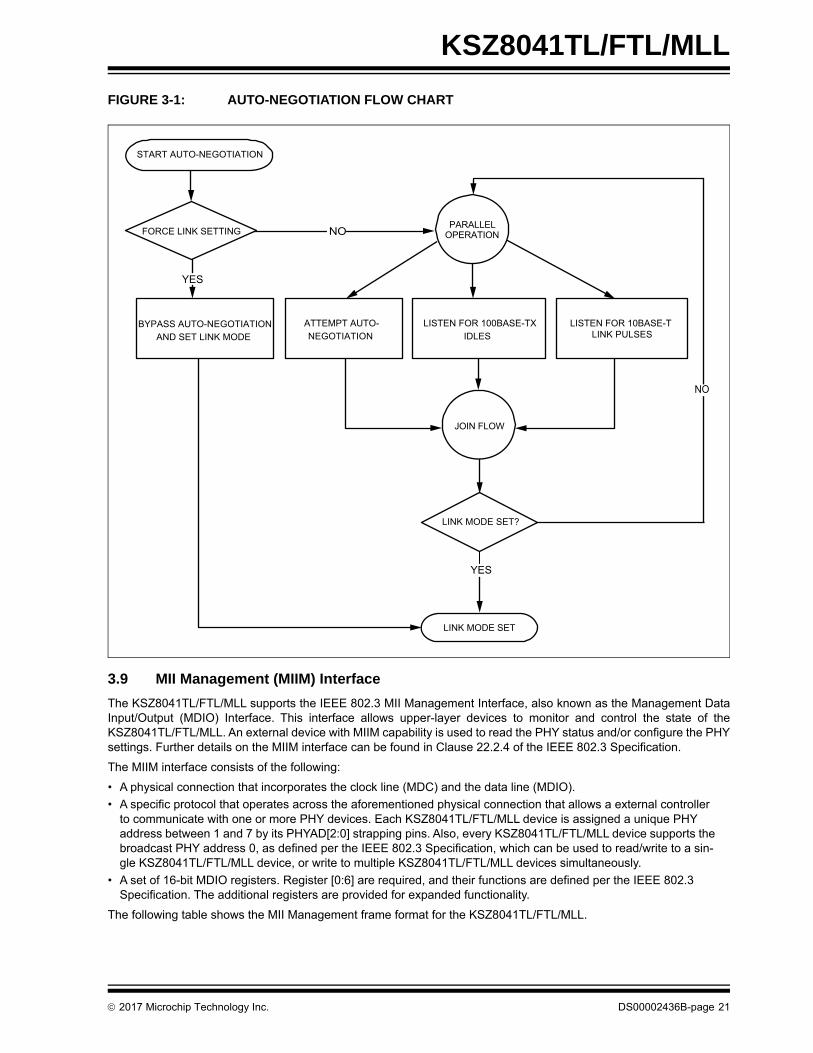
3.8 Auto-Negotiation
The KSZ8041TL/FTL/MLL conforms to the auto-negotiation protocol, defined in Clause 28 of the IEEE 802.3u specifi-cation. Auto-negotiation is enabled by either hardware pin strapping (pin 42) or software (register 0h bit 12).
Auto-negotiation allows unshielded twisted pair (UTP) link partners to select the highest common mode of operation.Link partners advertise their capabilities to each other, and then compare their own capabilities with those they receivedfrom their link partners. The highest speed and duplex setting that is common to the two link partners is selected as themode of operation.
The following list shows the speed and duplex operation mode from highest to lowest.
• Priority 1: 100BASE-TX, full-duplex
• Priority 2: 100BASE-TX, half-duplex
• Priority 3: 10BASE-T, full-duplex
• Priority 4: 10BASE-T, half-duplex
If auto-negotiation is not supported or the KSZ8041TL/FTL/MLL link partner is forced to bypass auto-negotiation, theKSZ8041TL/FTL/MLL sets its operating mode by observing the signal at its receiver. This is known as parallel detection,and allows the KSZ8041TL/FTL/MLL to establish link by listening for a fixed signal protocol in the absence of auto-nego-tiation advertisement protocol.
The auto-negotiation link up process is shown in the following flow chart.
DS00002436B-page 20 2017 Microchip Technology Inc.
KSZ8041TL/FTL/MLL
FIGURE 3-1: AUTO-NEGOTIATION FLOW CHART
3.9 MII Management (MIIM) Interface
The KSZ8041TL/FTL/MLL supports the IEEE 802.3 MII Management Interface, also known as the Management DataInput/Output (MDIO) Interface. This interface allows upper-layer devices to monitor and control the state of theKSZ8041TL/FTL/MLL. An external device with MIIM capability is used to read the PHY status and/or configure the PHYsettings. Further details on the MIIM interface can be found in Clause 22.2.4 of the IEEE 802.3 Specification.
The MIIM interface consists of the following:
• A physical connection that incorporates the clock line (MDC) and the data line (MDIO).
• A specific protocol that operates across the aforementioned physical connection that allows a external controller to communicate with one or more PHY devices. Each KSZ8041TL/FTL/MLL device is assigned a unique PHY address between 1 and 7 by its PHYAD[2:0] strapping pins. Also, every KSZ8041TL/FTL/MLL device supports the broadcast PHY address 0, as defined per the IEEE 802.3 Specification, which can be used to read/write to a sin-gle KSZ8041TL/FTL/MLL device, or write to multiple KSZ8041TL/FTL/MLL devices simultaneously.
• A set of 16-bit MDIO registers. Register [0:6] are required, and their functions are defined per the IEEE 802.3 Specification. The additional registers are provided for expanded functionality.
The following table shows the MII Management frame format for the KSZ8041TL/FTL/MLL.
START AUTO-NEGOTIATION
FORCE LINK SETTING
LISTEN FOR 10BASE-T LINK PULSES
LISTEN FOR 100BASE-TXIDLES
ATTEMPT AUTO-NEGOTIATION
LINK MODE SET
BYPASS AUTO-NEGOTIATIONAND SET LINK MODE
LINK MODE SET?
PARALLELOPERATIONNO
YES
YES
NO
JOIN FLOW
2017 Microchip Technology Inc. DS00002436B-page 21
KSZ8041TL/FTL/MLL
3.10 Interrupt (INTRP)
INTRP (pin 32) is an optional interrupt signal that is used to inform the external controller that there has been a statusupdate to the KSZ8041TL/FTL/MLL PHY register. Bits[15:8] of register 1Bh are the interrupt control bits, and are usedto enable and disable the conditions for asserting the INTRP signal. Bits[7:0] of register 1Bh are the interrupt status bits,and are used to indicate which interrupt conditions have occurred. The interrupt status bits are cleared after readingregister 1Bh.
Bit 9 of register 1Fh sets the interrupt level to active-high or active-low.
3.11 MII Data Interface
The Media Independent Interface (MII) is specified in Clause 22 of the IEEE 802.3 Specification. It provides a commoninterface between physical layer and MAC layer devices, and has the following key characteristics:
• Supports 10 Mbps and 100 Mbps data rates.
• Uses a 25 MHz reference clock, sourced by the PHY.
• Provides independent 4-bit wide (nibble) transmit and receive data paths.
• Contains two distinct groups of signals: one for transmission and the other for reception.
By default, the KSZ8041TL/FTL/MLL is configured to MII mode after it is power-up or reset with the following:
• A 25 MHz crystal connected to XI, XO (pins 15, 14), or an external 25 MHz clock source (oscillator) connected to XI.
• CONFIG[2:0] (pins 27, 41, 40) set to ‘000’ (default setting).
3.12 MII Signal Definition
The following table describes the MII signals. Refer to Clause 22 of the IEEE 802.3 Specification for detailed information.
3.12.1 TRANSMIT CLOCK (TXC)
TXC is sourced by the PHY. It is a continuous clock that provides the timing reference for TXEN and TXD[3:0].
TXC is 2.5 MHz for 10 Mbps operation and 25 MHz for 100 Mbps operation.
TABLE 3-1: MII MANAGEMENT FRAME FORMAT
— PreambleStart
of Frame
R/WOP
Code
PHYAddressBits[4:0]
REGAddressBits[4:0]
TA Data Bits [15:0] Idle
Read 32 1’s 01 10 00AAA RRRRR Z0 DDDDDDDD_DDDDDDDD Z
Write 32 1’s 01 01 00AAA RRRRR 10 DDDDDDDD_DDDDDDDD Z
TABLE 3-2: MII SIGNAL DEFINITIONS
MII Signal Name
Direction with Respect to PHY
Direction with Respect to MAC
Description
TXC Output Input Transmit Clock (2.5 MHz for 10 Mbps; 25 MHz for 100 Mbps)
TXEN Input Output Transmit Enable
TXD[3:0] Input Output Transmit Data [3:0]
RXC Output Input Receive Clock (2.5 MHz for 10 Mbps; 25 MHz for 100 Mbps)
RXDV Output Input Receive Data Valid
RXD[3:0] Output Input Receive Data [3:0]
RXER Output Input or not required Receive Error
CRS Output Input Carrier Sense
COL Output Input Collision Detection
DS00002436B-page 22 2017 Microchip Technology Inc.
KSZ8041TL/FTL/MLL
3.12.2 TRANSMIT ENABLE (TXEN)
TXEN indicates the MAC is presenting nibbles on TXD[3:0] for transmission. It is asserted synchronously with the firstnibble of the preamble and remains asserted while all nibbles to be transmitted are presented on the MII, and is negatedprior to the first TXC following the final nibble of a frame.
TXEN transitions synchronously with respect to TXC.
3.12.3 TRANSMIT DATA [3:0] (TXD[3:0])
TXD[3:0] transitions synchronously with respect to TXC. When TXEN is asserted, TXD[3:0] are accepted for transmis-sion by the PHY. TXD[3:0] is “00” to indicate idle when TXEN is de-asserted. Values other than “00” on TXD[3:0] whileTXEN is de-asserted are ignored by the PHY.
3.12.4 RECEIVE CLOCK (RXC)
RXC provides the timing reference for RXDV, RXD[3:0], and RXER.
• In 10 Mbps mode, RXC is recovered from the line while carrier is active. RXC is derived from the PHY’s reference clock when the line is idle, or link is down.
• In 100 Mbps mode, RXC is continuously recovered from the line. If link is down, RXC is derived from the PHY’s reference clock.
RXC is 2.5 MHz for 10 Mbps operation and 25 MHz for 100 Mbps operation.
3.12.5 RECEIVE DATA VALID (RXDV)
RXDV is driven by the PHY to indicate that the PHY is presenting recovered and decoded nibbles on RXD[3:0].
• In 10 Mbps mode, RXDV is asserted with the first nibble of the Start of Frame Delimiter (SFD), “5D”, and remains asserted until the end of the frame.
• In 100 Mbps mode, RXDV is asserted from the first nibble of the preamble to the last nibble of the frame.
RXDV transitions synchronously with respect to RXC.
3.12.6 RECEIVE DATA [3:0] (RXD[3:0])
RXD[3:0] transitions synchronously with respect to RXC. For each clock period in which RXDV is asserted, RXD[3:0]transfers a nibble of recovered data from the PHY.
3.12.7 RECEIVE ERROR (RXER)
RXER is asserted for one or more RXC periods to indicate that a Symbol Error (e.g. a coding error that a PHY is capableof detecting, and that may otherwise be undetectable by the MAC sub-layer) was detected somewhere in the framepresently being transferred from the PHY.
RXER transitions synchronously with respect to RXC. While RXDV is de-asserted, RXER has no effect on the MAC.
3.12.8 CARRIER SENSE (CRS)
CRS is asserted and de-asserted as follows:
• In 10 Mbps mode, CRS assertion is based on the reception of valid preambles. CRS de-assertion is based on the reception of an end-of-frame (EOF) marker.
• In 100 Mbps mode, CRS is asserted when a start-of-stream delimiter, or /J/K symbol pair is detected. CRS is de-asserted when an end-of-stream delimiter, or /T/R symbol pair is detected. Additionally, the PMA layer de-asserts CRS if IDLE symbols are received without /T/R.
3.12.9 COLLISION (COL)
COL is asserted in half-duplex mode whenever the transmitter and receiver are simultaneously active on the line. Thisis used to inform the MAC that a collision has occurred during its transmission to the PHY.
COL transitions asynchronously with respect to TXC and RXC.
3.13 Reduced MII (RMII) Data Interface (KSZ8041TL/FTL Only)
The Reduced Media Independent Interface (RMII) specifies a low pin count Media Independent Interface (MII). It pro-vides a common interface between physical layer and MAC layer devices, and has the following key characteristics:
2017 Microchip Technology Inc. DS00002436B-page 23
KSZ8041TL/FTL/MLL
• Supports 10 Mbps and 100 Mbps data rates.
• Uses a single 50 MHz reference clock provided by the MAC or the system board.
• Provides independent 2-bit wide (di-bit) transmit and receive data paths.
• Contains two distinct groups of signals: one for transmission and the other for reception.
The KSZ8041TL/FTL is configured in RMII mode after it is power-up or reset with the following:
• A 50 MHz reference clock connected to REFCLK (pin 15).
• CONFIG[2:0] (pins 27, 41, 40) set to ‘001’.
In RMII mode, unused MII signals, TXD[3:2] (pins 39, 38), are tied to ground.
3.14 RMII Signal Definition (KSZ8041TL/FTL Only)
The following table describes the RMII signals. Refer to RMII Specification for detailed information.
3.14.1 REFERENCE CLOCK (REF_CLK)
REF_CLK is sourced by the MAC or system board. It is a continuous 50 MHz clock that provides the timing referencefor TX_EN, TXD[1:0], CRS_DV, RXD[1:0], and RX_ER.
3.14.2 TRANSMIT ENABLE (TX_EN)
TX_EN indicates that the MAC is presenting di-bits on TXD[1:0] for transmission. It is asserted synchronously with thefirst nibble of the preamble and remains asserted while all di-bits to be transmitted are presented on the RMII, and isnegated prior to the first REF_CLK following the final di-bit of a frame.
TX_EN transitions synchronously with respect to REF_CLK.
3.14.3 TRANSMIT DATA [1:0] (TXD[1:0])
TXD[1:0] transitions synchronously with respect to REF_CLK. When TX_EN is asserted, TXD[1:0] are accepted fortransmission by the PHY. TXD[1:0] is “00” to indicate idle when TX_EN is de-asserted. Values other than “00” onTXD[1:0] while TX_EN is de-asserted are ignored by the PHY.
3.14.4 CARRIER SENSE/RECEIVE DATA VALID (CRS_DV)
CRS_DV is asserted by the PHY when the receive medium is non-idle. It is asserted asynchronously on detection ofcarrier. This is when squelch is passed in 10 Mbps mode, and when two non-contiguous zeroes in 10 bits are detectedin 100 Mbps mode. Loss of carrier results in the de-assertion of CRS_DV.
So long as carrier detection criteria are met, CRS_DV remains asserted continuously from the first recovered di-bit ofthe frame through the final recovered di-bit, and it is negated prior to the first REF_CLK that follows the final di-bit. Thedata on RXD[1:0] is considered valid once CRS_DV is asserted. However, since the assertion of CRS_DV is asynchro-nous relative to REF_CLK, the data on RXD[1:0] is “00” until proper receive signal decoding takes place.
3.14.5 RECEIVE DATA [1:0] (RXD[1:0])
RXD[1:0] transitions synchronously to REF_CLK. For each clock period in which CRS_DV is asserted, RXD[1:0] trans-fers two bits of recovered data from the PHY. RXD[1:0] is “00” to indicate idle when CRS_DV is de-asserted. Valuesother than “00” on RXD[1:0] while CRS_DV is de-asserted are ignored by the MAC.
TABLE 3-3: RMII SIGNAL DEFINITIONS
RMII Signal Name
Direction with Respect to PHY
Direction with Respect to MAC
Description
REF_CLK Input Input or Output Synchronous 50 MHz clock reference for receive, transmit and control interface
TX_EN Input Output Transmit Enable
TXD[1:0] Input Output Transmit Data [1:0]
CRS_DV Output Input Carrier Sense/Receive Data Valid
RXD[1:0] Output Input Receive Data [1:0]
RX_ER Output Input or not required Receive Error
DS00002436B-page 24 2017 Microchip Technology Inc.

KSZ8041TL/FTL/MLL
3.14.6 RECEIVE ERROR (RX_ER)
RX_ER is asserted for one or more REF_CLK periods to indicate that a Symbol Error (e.g. a coding error that a PHY iscapable of detecting, and that may otherwise be undetectable by the MAC sub-layer) was detected somewhere in theframe presently being transferred from the PHY.
RX_ER transitions synchronously with respect to REF_CLK. While CRS_DV is de-asserted, RX_ER has no effect onthe MAC.
3.14.7 COLLISION DETECTION
The MAC regenerates the COL signal of the MII from TX_EN and CRS_DV.
3.15 Serial MII (SMII) Data Interface (KSZ8041TL/FTL Only)
The Serial Media Independent Interface (SMII) is the lowest pin count Media Independent Interface (MII). It provides acommon interface between physical layer and MAC layer devices, and has the following key characteristics:
• Supports 10 Mbps and 100 Mbps data rates.
• Uses 125 MHz reference clock provided by the MAC or the system board.
• Uses 12.5 MHz sync pulse provided by the MAC.
• Provides independent single-bit wide transmit and receive data paths for data and control information.
The KSZ8041TL/FTL is configured in SMII mode after it is power-up or reset with the following:
• A 125 MHz reference clock connected to CLOCK (pin 15).
• A 12.5 MHz sync pulse connected to SYNC (pin 36).
• CONFIG[2:0] (pins 27, 41, 40) set to ‘010’.
In SMII mode, unused MII signals, TXD[3:2] (pins 39, 38), are tied to ground.
3.16 SMII Signal Definition (KSZ8041TL/FTL Only)
The following table describes the SMII signals. Refer to SMII Specification for detailed information.
3.16.1 CLOCK REFERENCE (CLOCK)
CLOCK is sourced by the MAC or system board. It is a continuous 125 MHz clock that provides the timing reference forSYNC, TX, and RX.
3.16.2 SYNC PULSE (SYNC)
SYNC is a 12.5 MHz synchronized pulse derived from CLOCK by the MAC. It is used to indicate the segment boundaryfor each transmit data/control segment, or receive data/control segment. Each segment is comprised of ten bits.
SYNC is generated continuously by the MAC at every ten cycles of CLOCK.
3.16.3 TRANSMIT DATA AND CONTROL (TX)
TX provides transmit data and control information from MAC-to-PHY in 10-bit segments.
• In 10 Mbps mode, each segment is repeated ten times. Therefore, every ten segments represent a new byte of data. The PHY can sample any one of every ten segments.
• In 100 Mbps mode, each segment represents a new byte of data.
TABLE 3-4: SMII SIGNAL DESCRIPTION
SMII Signal Name
Direction with Respect to PHY
Direction with Respect to MAC
Description
CLOCK Input Input or Output 125 MHz clock reference for receive and transmit data and control
SYNC Input Output 12.5 MHz sync pulse from MAC
TX Input Output Transmit Data and Control
RX Output Input Receive Data and Control
2017 Microchip Technology Inc. DS00002436B-page 25
KSZ8041TL/FTL/MLL
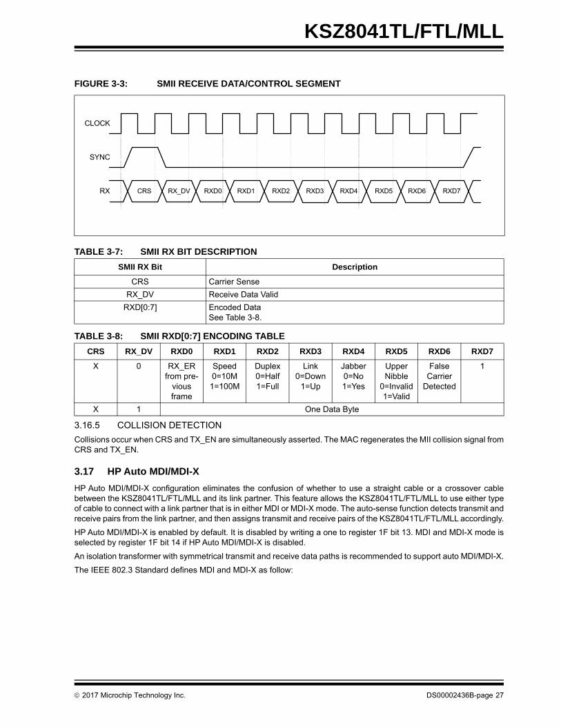
3.16.4 RECEIVE DATA AND CONTROL (RX)
RX provides receive data and control information from PHY-to-MAC in 10-bit segments.
• In 10 Mbps mode, each segment is repeated ten times. Therefore, every ten segments represent a new byte of data. The MAC can sample any one of every ten segments.
• In 100 Mbps mode, each segment represents a new byte of data.
The following figure and tables show the receive data/control format for each segment:
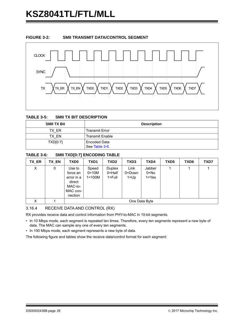
FIGURE 3-2: SMII TRANSMIT DATA/CONTROL SEGMENT
TABLE 3-5: SMII TX BIT DESCRIPTION
SMII TX Bit Description
TX_ER Transmit Error
TX_EN Transmit Enable
TXD[0:7] Encoded DataSee Table 3-6.
TABLE 3-6: SMII TXD[0:7] ENCODING TABLE
TX_ER TX_EN TXD0 TXD1 TXD2 TXD3 TXD4 TXD5 TXD6 TXD7
X 0 Use to force an error in a
direct MAC-to-
MAC con-nection
Speed0=10M
1=100M
Duplex0=Half 1=Full
Link0=Down
1=Up
Jabber0=No 1=Yes
1 1 1
X 1 One Data Byte
TX_ER TX_EN TXD0 TXD1 TXD2 TXD3 TXD4 TXD5 TXD6 TXD7
CLOCK
SYNC
TX
DS00002436B-page 26 2017 Microchip Technology Inc.
KSZ8041TL/FTL/MLL
3.16.5 COLLISION DETECTION
Collisions occur when CRS and TX_EN are simultaneously asserted. The MAC regenerates the MII collision signal fromCRS and TX_EN.
3.17 HP Auto MDI/MDI-X
HP Auto MDI/MDI-X configuration eliminates the confusion of whether to use a straight cable or a crossover cablebetween the KSZ8041TL/FTL/MLL and its link partner. This feature allows the KSZ8041TL/FTL/MLL to use either typeof cable to connect with a link partner that is in either MDI or MDI-X mode. The auto-sense function detects transmit andreceive pairs from the link partner, and then assigns transmit and receive pairs of the KSZ8041TL/FTL/MLL accordingly.
HP Auto MDI/MDI-X is enabled by default. It is disabled by writing a one to register 1F bit 13. MDI and MDI-X mode isselected by register 1F bit 14 if HP Auto MDI/MDI-X is disabled.
An isolation transformer with symmetrical transmit and receive data paths is recommended to support auto MDI/MDI-X.
The IEEE 802.3 Standard defines MDI and MDI-X as follow:
FIGURE 3-3: SMII RECEIVE DATA/CONTROL SEGMENT
TABLE 3-7: SMII RX BIT DESCRIPTION
SMII RX Bit Description
CRS Carrier Sense
RX_DV Receive Data Valid
RXD[0:7] Encoded DataSee Table 3-8.
TABLE 3-8: SMII RXD[0:7] ENCODING TABLE
CRS RX_DV RXD0 RXD1 RXD2 RXD3 RXD4 RXD5 RXD6 RXD7
X 0 RX_ER from pre-
vious frame
Speed0=10M
1=100M
Duplex0=Half 1=Full
Link0=Down
1=Up
Jabber0=No 1=Yes
Upper Nibble
0=Invalid 1=Valid
False Carrier
Detected
1
X 1 One Data Byte
CRS RX_DV RXD0 RXD1 RXD2 RXD3 RXD4 RXD5 RXD6 RXD7
CLOCK
SYNC
RX
2017 Microchip Technology Inc. DS00002436B-page 27

KSZ8041TL/FTL/MLL
3.17.1 STRAIGHT CABLE
A straight cable connects an MDI device to an MDI-X device, or an MDI-X device to an MDI device. Figure 3-4 depictsa typical straight cable connection between a network interface card (NIC) and a switch, or hub (MDI-X).
TABLE 3-9: MDI/MDI-X PIN DEFINITION
MDI MDI-X
RJ-45 Pin Signal RJ-45 Pin Signal
1 TD+ 1 RD+
2 TD– 2 RD–
3 RD+ 3 TD+
6 RD– 6 TD–
FIGURE 3-4: TYPICAL STRAIGHT CABLE CONNECTION
Receive PairTransmit Pair
Receive Pair
1
2
3
4
5
6
7
8
1
2
3
4
5
6
7
8
Transmit Pair
Modular Connector(RJ-45)
NIC
StraightCable
10/100 EthernetMedia Dependent Interface
10/100 EthernetMedia Dependent Interface
Modular Connector(RJ-45)
HUB(Repeater or Switch)
DS00002436B-page 28 2017 Microchip Technology Inc.

KSZ8041TL/FTL/MLL
3.17.2 CROSSOVER CABLE
A crossover cable connects an MDI device to another MDI device, or an MDI-X device to another MDI-X device.Figure 3-5 shows a typical crossover cable connection between two switches or hubs (two MDI-X devices).
3.18 LinkMD® Cable Diagnostics
The LinkMD® feature utilizes time domain reflectometry (TDR) to analyze the cabling plant for common cabling prob-lems, such as open circuits, short circuits and impedance mismatches.
LinkMD® works by sending a pulse of known amplitude and duration down the MDI and MDI-X pairs, and then analyzingthe shape of the reflected signal. Timing the pulse duration gives an indication of the distance to the cabling fault withmaximum distance of 200m and accuracy of ±2m. Internal circuitry computes the TDR information and presents it in auser-readable digital format.
Cable diagnostics are only valid for copper connections and do not support fiber optic operation.
3.18.1 ACCESS
LinkMD is initiated by accessing register 1Dh, the LinkMD Control/Status Register, in conjunction with register 1Fh, thePHY Control 2 Register.
3.18.2 USAGE
The following test procedure demonstrates how to use LinkMD for cable diagnostic:
1. Disable auto MDI/MDI-X by writing a ‘1’ to register 1Fh bit 13 to enable manual control over the differential pairused to transmit the LinkMD pulse.
2. Select the differential pair to transmit the LinkMD pulse with register 1Fh bit 14.
3. Start cable diagnostic test by writing a ‘1’ to register 1Dh bit 15. This enable bit is self-clearing.
FIGURE 3-5: TYPICAL CROSSOVER CABLE CONNECTION
Receive Pair Receive Pair
Transmit Pair
1
2
3
4
5
6
7
8
1
2
3
4
5
6
7
8
Transmit Pair
10/100 EthernetMedia Dependent Interface
10/100 EthernetMedia Dependent Interface
Modular Connector (RJ-45)HUB
(Repeater or Switch)
Modular Connector (RJ-45)HUB
(Repeater or Switch)
CrossoverCable
2017 Microchip Technology Inc. DS00002436B-page 29
KSZ8041TL/FTL/MLL
4. Wait (poll) for register 1Dh bit 15 to return a ‘0’, indicating cable diagnostic test is completed.
5. Read cable diagnostic test results in register 1Dh bits [14:13]. The results are as follows:
00 = Valid test, normal condition
01 = Valid test, open circuit in cable
10 = Valid test, short circuit in cable
11 = Invalid test, cable diagnostic test failed
The ‘11’ case, invalid test, occurs if the KSZ8041TL/FTL/MLL is unable to shut down the link partner. In this instance,the test is not run because it would be impossible for the KSZ8041TL/FTL/MLL to determine if the detected signal is areflection of the signal generated by the KSZ8041TL/FTL/MLL, or a signal from its link partner.
6. Get distance to fault by multiplying the decimal value in register 1Dh bits [8:0] by a constant of 0.4. The distance,D (expressed in meters), to the cable fault is determined by the following formula:
D (distance to cable fault) = 0.4 x decimal value of register 1Dh bits [8:0]
The 0.4 constant may be calibrated for different cable types and cabling conditions, including cables with a velocity ofpropagation that varies significantly from the norm.
3.19 Power Management
The KSZ8041TL/FTL/MLL offers the following power management modes:
3.19.1 POWER SAVING MODE
This mode is used to reduce power consumption when the cable is unplugged. It is in effect when auto-negotiation modeis enabled, cable is disconnected, and register 1Fh bit 10 is set to 1. Under power saving mode, the KSZ8041TL/FTL/MLL shuts down all transceiver blocks, except for transmitter, energy detect and PLL circuits. Additionally, in MII mode,the RXC clock output is disabled. RXC clock is enabled after the cable is connected and link is established.
Power saving mode is disabled by writing a zero to register 1Fh bit 10.
3.19.2 POWER DOWN MODE
This mode is used to power down the entire KSZ8041TL/FTL/MLL device when it is not in use. Power down mode isenabled by writing a one to register 0h bit 11. In the power down state, the KSZ8041TL/FTL/MLL disables all internalfunctions, except for the MII management interface.
3.20 Reference Clock Connection Options
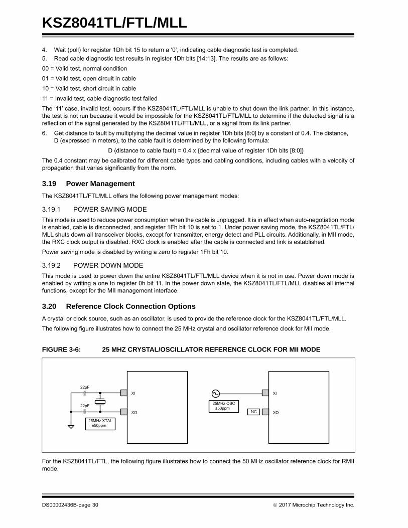
A crystal or clock source, such as an oscillator, is used to provide the reference clock for the KSZ8041TL/FTL/MLL.
The following figure illustrates how to connect the 25 MHz crystal and oscillator reference clock for MII mode.
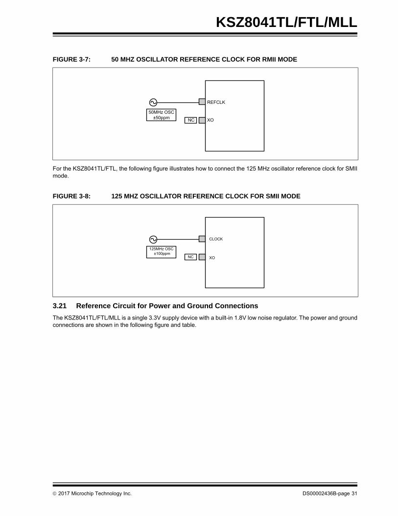
For the KSZ8041TL/FTL, the following figure illustrates how to connect the 50 MHz oscillator reference clock for RMIImode.
FIGURE 3-6: 25 MHZ CRYSTAL/OSCILLATOR REFERENCE CLOCK FOR MII MODE
25MHz OSC ±50ppm
NCNC
XI
XO
XI
XO
22pF
22pF
25MHz XTAL ±50ppm
DS00002436B-page 30 2017 Microchip Technology Inc.
KSZ8041TL/FTL/MLL
For the KSZ8041TL/FTL, the following figure illustrates how to connect the 125 MHz oscillator reference clock for SMIImode.
3.21 Reference Circuit for Power and Ground Connections
The KSZ8041TL/FTL/MLL is a single 3.3V supply device with a built-in 1.8V low noise regulator. The power and groundconnections are shown in the following figure and table.
FIGURE 3-7: 50 MHZ OSCILLATOR REFERENCE CLOCK FOR RMII MODE
FIGURE 3-8: 125 MHZ OSCILLATOR REFERENCE CLOCK FOR SMII MODE
REFCLK
XONC
50MHz OSC±50ppm
125MHz OSC ±100ppm
NC
CLOCK
XO
2017 Microchip Technology Inc. DS00002436B-page 31
KSZ8041TL/FTL/MLL
3.22 100BASE-FX Fiber Operation (KSZ8041FTL Only)
100BASE-FX fiber operation is similar to 100BASE-TX copper operation with the differences being that the scrambler/de-scrambler and MLT3 encoder/decoder are bypassed on transmission and reception. In addition, auto-negotiation isbypassed, auto MDI/MDI-X is disabled, and speed is set to 100 Mbps. The duplex can be set to either half or full. Usu-ally, it is set to full-duplex.
3.22.1 FIBER SIGNAL DETECT
In 100BASE-FX operation, FXSD (fiber signal detect), input pin 48, is usually connected to the fiber transceiver SD (sig-nal detect) output pin. 100BASE-FX mode is activated when the FXSD input pin is greater than 1V. When FXSD isbetween 1V and 1.8V, no fiber signal is detected and a Far-End Fault is generated. When FXSD is over 2.2V, the fibersignal is detected.
100BASE-FX mode and signal detection is summarized in the following table:
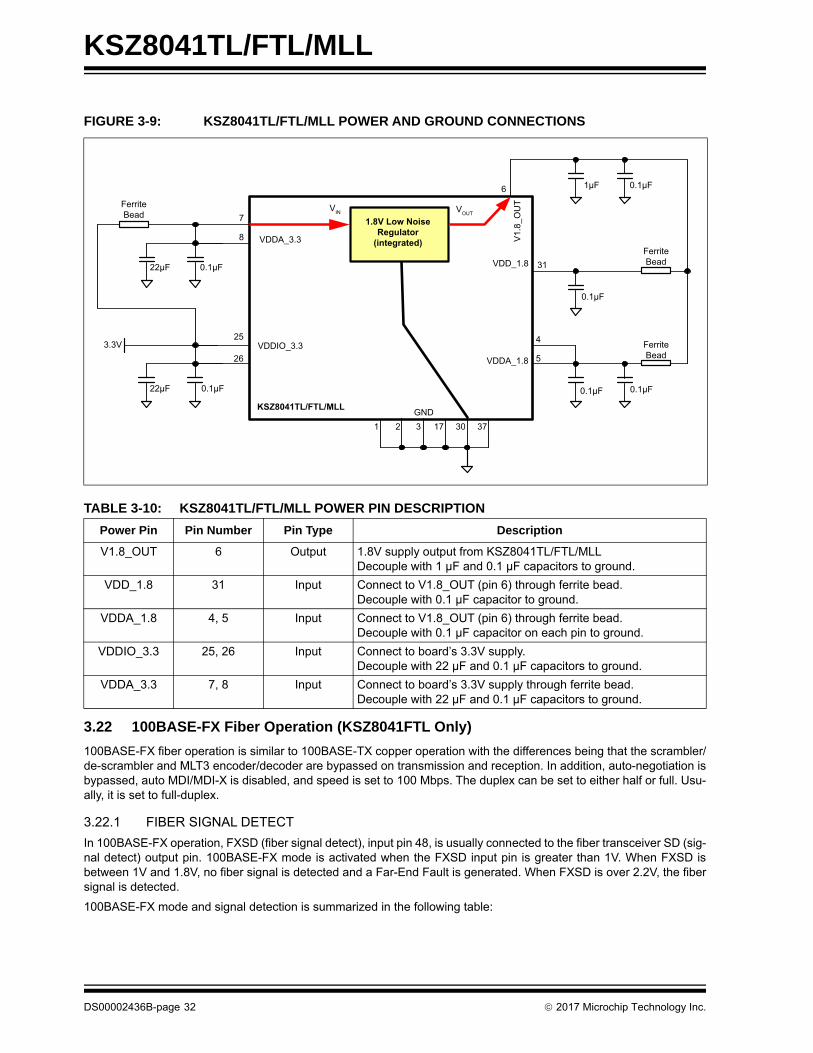
FIGURE 3-9: KSZ8041TL/FTL/MLL POWER AND GROUND CONNECTIONS
TABLE 3-10: KSZ8041TL/FTL/MLL POWER PIN DESCRIPTION
Power Pin Pin Number Pin Type Description
V1.8_OUT 6 Output 1.8V supply output from KSZ8041TL/FTL/MLLDecouple with 1 µF and 0.1 µF capacitors to ground.
VDD_1.8 31 Input Connect to V1.8_OUT (pin 6) through ferrite bead.Decouple with 0.1 µF capacitor to ground.
VDDA_1.8 4, 5 Input Connect to V1.8_OUT (pin 6) through ferrite bead.Decouple with 0.1 µF capacitor on each pin to ground.
VDDIO_3.3 25, 26 Input Connect to board’s 3.3V supply.Decouple with 22 µF and 0.1 µF capacitors to ground.
VDDA_3.3 7, 8 Input Connect to board’s 3.3V supply through ferrite bead.Decouple with 22 µF and 0.1 µF capacitors to ground.
FerriteBead 7
8
3.3V
22μF 0.1μF
25
26
22μF 0.1μF
VIN
VDDA_3.3
VDDIO_3.3
KSZ8041TL/FTL/MLL
1.8V Low NoiseRegulator
(integrated)
GND
VDDA_1.8
VDD_1.8
V1.
8_O
UT
VOUT
1 2 3 17 30 37
4
5
0.1μF 0.1μF
0.1μF
FerriteBead
FerriteBead
0.1μF1μF
31
6
DS00002436B-page 32 2017 Microchip Technology Inc.

KSZ8041TL/FTL/MLL
To ensure proper operation, a resistive voltage divider is recommended to adjust the fiber transceiver SD (signal detect)output voltage swing to match the FXSD pin’s input voltage threshold.
Alternatively, the Far-End Fault feature can be disabled. In this case, the FXSD input pin is tied high to 3.3V to force100BASE-FX mode.
3.22.2 FAR-END FAULT
A Far-End Fault (FEF) occurs when the signal detection is logically false on the receive side of the fiber transceiver. TheKSZ8041FTL detects a FEF when its FXSD input (pin 48) is between 1V and 1.8V. When a FEF is detected, theKSZ8041FTL signals its fiber link partner that a FEF has occurred by transmitting a repetitive pattern of 84-ones and 1-zero. This pattern is used to inform the fiber link partner that there is a faulty link on its transmit side.
By default, FEF is enabled. FEF is disabled by strapping “no FEF” (pin 43) low. See the Strap-In Options section fordetail.
3.23 Back-to-Back Media Converter
A KSZ8041TL/MLL and a KSZ8041FTL can be connected back-to-back to provide a low cost media converter solution.In back-to-back mode, media conversion is between 100BASE-TX copper and 100BASE-FX fiber. On the copper side,link up at 10BASE-T is not allowed, and is blocked during auto-negotiation.
3.23.1 MII BACK-TO-BACK MODE
In MII Back-to-Back mode, the KSZ8041TL/MLL interfaces with another KSZ8041TL/MLL, or a KSZ8041FTL to providea complete 100 Mbps repeater or media converter solution. The KSZ8041TL/FTL/MLL devices are configured to MIIBack-to-Back mode after they are power-up or reset with the following:
• CONFIG[2:0] (pins 27, 41, 40) set to ‘110’
• A common 25 MHz reference clock connected to XI (pin 15)
• MII signals connected as shown in the following table.
TABLE 3-11: COPPER AND FIBER MODE SELECTION
FXSD Input Voltage Mode
Less than 0.2V Copper mode
Greater than 1V, but less than 1.8V Fiber modeNo signal detected
Far-End Fault generated (if enabled)
Greater than 2.2V Fiber modeSignal detected
FIGURE 3-10: KSZ8041TL/MLL AND KSZ8041FTL BACK-TO-BACK MEDIA CONVERTER
RX+/-
TX+/-KSZ8041TL/MLL(Copper Mode)
RxD
TxD
25MHz
OSC
XI
XI
TxD
RxD
KSZ8041FTL(Fiber Mode)
FXSDFiberSignalDetect
Fiber RX
Fiber TX
2017 Microchip Technology Inc. DS00002436B-page 33
KSZ8041TL/FTL/MLL
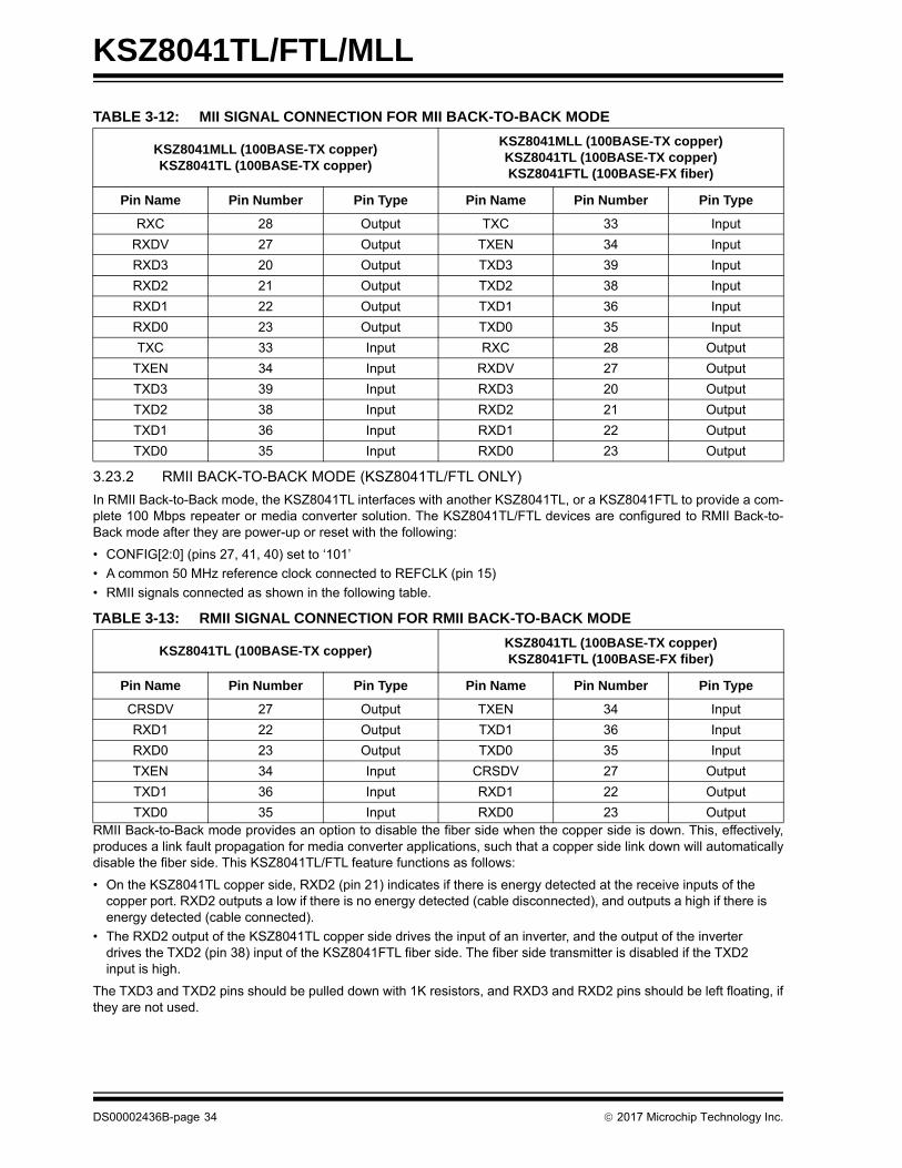
3.23.2 RMII BACK-TO-BACK MODE (KSZ8041TL/FTL ONLY)
In RMII Back-to-Back mode, the KSZ8041TL interfaces with another KSZ8041TL, or a KSZ8041FTL to provide a com-plete 100 Mbps repeater or media converter solution. The KSZ8041TL/FTL devices are configured to RMII Back-to-Back mode after they are power-up or reset with the following:
• CONFIG[2:0] (pins 27, 41, 40) set to ‘101’
• A common 50 MHz reference clock connected to REFCLK (pin 15)
• RMII signals connected as shown in the following table.
RMII Back-to-Back mode provides an option to disable the fiber side when the copper side is down. This, effectively,produces a link fault propagation for media converter applications, such that a copper side link down will automaticallydisable the fiber side. This KSZ8041TL/FTL feature functions as follows:
• On the KSZ8041TL copper side, RXD2 (pin 21) indicates if there is energy detected at the receive inputs of the copper port. RXD2 outputs a low if there is no energy detected (cable disconnected), and outputs a high if there is energy detected (cable connected).
• The RXD2 output of the KSZ8041TL copper side drives the input of an inverter, and the output of the inverter drives the TXD2 (pin 38) input of the KSZ8041FTL fiber side. The fiber side transmitter is disabled if the TXD2 input is high.
The TXD3 and TXD2 pins should be pulled down with 1K resistors, and RXD3 and RXD2 pins should be left floating, ifthey are not used.
TABLE 3-12: MII SIGNAL CONNECTION FOR MII BACK-TO-BACK MODE
KSZ8041MLL (100BASE-TX copper)KSZ8041TL (100BASE-TX copper)
KSZ8041MLL (100BASE-TX copper)KSZ8041TL (100BASE-TX copper)KSZ8041FTL (100BASE-FX fiber)
Pin Name Pin Number Pin Type Pin Name Pin Number Pin Type
RXC 28 Output TXC 33 Input
RXDV 27 Output TXEN 34 Input
RXD3 20 Output TXD3 39 Input
RXD2 21 Output TXD2 38 Input
RXD1 22 Output TXD1 36 Input
RXD0 23 Output TXD0 35 Input
TXC 33 Input RXC 28 Output
TXEN 34 Input RXDV 27 Output
TXD3 39 Input RXD3 20 Output
TXD2 38 Input RXD2 21 Output
TXD1 36 Input RXD1 22 Output
TXD0 35 Input RXD0 23 Output
TABLE 3-13: RMII SIGNAL CONNECTION FOR RMII BACK-TO-BACK MODE
KSZ8041TL (100BASE-TX copper)KSZ8041TL (100BASE-TX copper)KSZ8041FTL (100BASE-FX fiber)
Pin Name Pin Number Pin Type Pin Name Pin Number Pin Type
CRSDV 27 Output TXEN 34 Input
RXD1 22 Output TXD1 36 Input
RXD0 23 Output TXD0 35 Input
TXEN 34 Input CRSDV 27 Output
TXD1 36 Input RXD1 22 Output
TXD0 35 Input RXD0 23 Output
DS00002436B-page 34 2017 Microchip Technology Inc.
KSZ8041TL/FTL/MLL
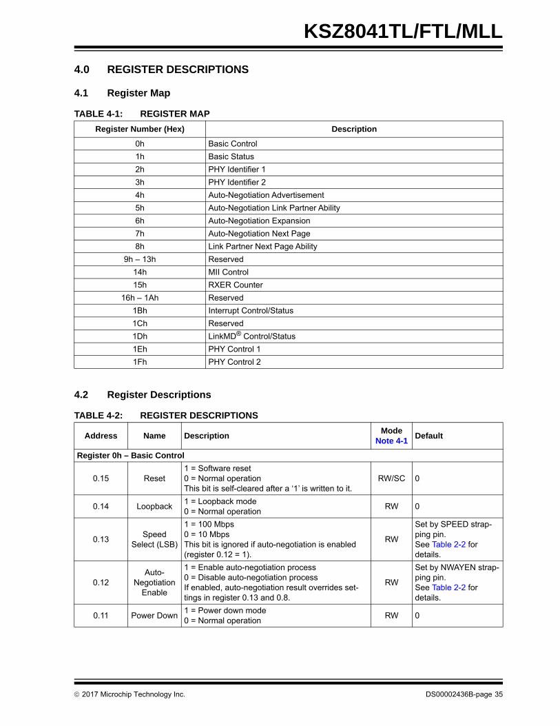
4.0 REGISTER DESCRIPTIONS
4.1 Register Map
4.2 Register Descriptions
TABLE 4-1: REGISTER MAP
Register Number (Hex) Description
0h Basic Control
1h Basic Status
2h PHY Identifier 1
3h PHY Identifier 2
4h Auto-Negotiation Advertisement
5h Auto-Negotiation Link Partner Ability
6h Auto-Negotiation Expansion
7h Auto-Negotiation Next Page
8h Link Partner Next Page Ability
9h – 13h Reserved
14h MII Control
15h RXER Counter
16h – 1Ah Reserved
1Bh Interrupt Control/Status
1Ch Reserved
1Dh LinkMD® Control/Status
1Eh PHY Control 1
1Fh PHY Control 2
TABLE 4-2: REGISTER DESCRIPTIONS
Address Name DescriptionMode
Note 4-1Default
Register 0h – Basic Control
0.15 Reset1 = Software reset0 = Normal operationThis bit is self-cleared after a ‘1’ is written to it.
RW/SC 0
0.14 Loopback1 = Loopback mode0 = Normal operation
RW 0
0.13Speed
Select (LSB)
1 = 100 Mbps0 = 10 MbpsThis bit is ignored if auto-negotiation is enabled (register 0.12 = 1).
RW
Set by SPEED strap-ping pin.See Table 2-2 for details.
0.12Auto-
Negotiation Enable
1 = Enable auto-negotiation process0 = Disable auto-negotiation processIf enabled, auto-negotiation result overrides set-tings in register 0.13 and 0.8.
RW
Set by NWAYEN strap-ping pin.See Table 2-2 for details.
0.11 Power Down1 = Power down mode0 = Normal operation
RW 0
2017 Microchip Technology Inc. DS00002436B-page 35
KSZ8041TL/FTL/MLL
0.10 Isolate1 = Electrical isolation of PHY from MII and TX+/TX–0 = Normal operation
RW
Set by ISO strapping pin.See Table 2-2 for details.
0.9Restart Auto-
Negotiation
1 = Restart auto-negotiation process0 = Normal operation.This bit is self-cleared after a ‘1’ is written to it.
RW/SC 0
0.8Duplex Mode
1 = Full-duplex0 = Half-duplex
RW
Inverse of DUPLEX strapping pin value.See Table 2-2 for details.
0.7Collision
Test1 = Enable COL test0 = Disable COL test
RW 0
0.6:1 Reserved — RO 000_000
0.0Disable
Transmitter0 = Enable transmitter1 = Disable transmitter
RW 0
Register 1h – Basic Status
1.15 100BASE-T41 = T4 capable0 = Not T4 capable
RO 0
1.14100BASE-
TX Full-Duplex
1 = Capable of 100 Mbps full-duplex0 = Not capable of 100 Mbps full-duplex
RO 1
1.13100BASE-TX Half-Duplex
1 = Capable of 100 Mbps half-duplex0 = Not capable of 100 Mbps half-duplex
RO 1
1.1210BASE-T Full-Duplex
1 = Capable of 10 Mbps full-duplex0 = Not capable of 10 Mbps full-duplex
RO 1
1.1110BASE-T Half-Duplex
1 = Capable of 10 Mbps half-duplex0 = Not capable of 10 Mbps half-duplex
RO 1
1.10:7 Reserved — RO 0000
1.6 No Preamble1 = Preamble suppression0 = Normal preamble
RO 1
1.5Auto-
Negotiation Complete
1 = Auto-negotiation process completed0 = Auto-negotiation process not completed
RO 0
1.4Remote
Fault1 = Remote fault0 = No remote fault
RO/LH 0
1.3Auto-
Negotiation Ability
1 = Capable to perform auto-negotiation0 = Not capable to perform auto-negotiation
RO 1
1.2 Link Status1 = Link is up0 = Link is down
RO/LL 0
1.1Jabber Detect
1 = Jabber detected0 = Jabber not detected (default is low)
RO/LH 0
1.0Extended Capability
1 = Supports extended capabilities registers RO 1
Register 2h – PHY Identifier 1
2.15:0PHY ID Number
Assigned to the 3rd through 18th bits of the Orga-nizationally Unique Identifier (OUI). Kendin Com-munication’s OUI is 0010A1 (hex).
RO 0022h
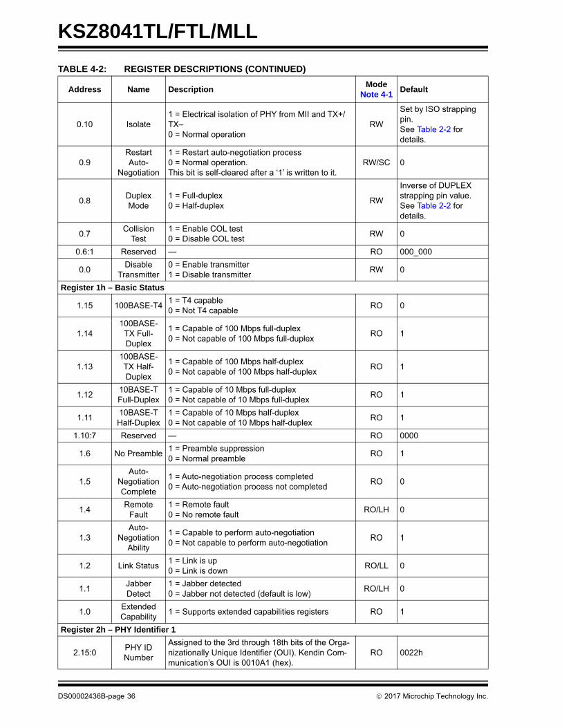
TABLE 4-2: REGISTER DESCRIPTIONS (CONTINUED)
Address Name DescriptionMode
Note 4-1Default
DS00002436B-page 36 2017 Microchip Technology Inc.
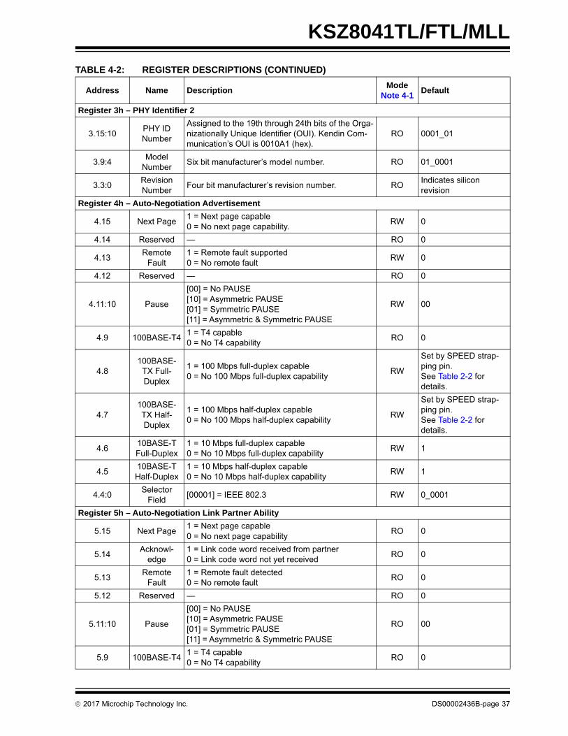
KSZ8041TL/FTL/MLL
Register 3h – PHY Identifier 2
3.15:10PHY ID Number
Assigned to the 19th through 24th bits of the Orga-nizationally Unique Identifier (OUI). Kendin Com-munication’s OUI is 0010A1 (hex).
RO 0001_01
3.9:4Model
NumberSix bit manufacturer’s model number. RO 01_0001
3.3:0Revision Number
Four bit manufacturer’s revision number. ROIndicates silicon revision
Register 4h – Auto-Negotiation Advertisement
4.15 Next Page1 = Next page capable0 = No next page capability.
RW 0
4.14 Reserved — RO 0
4.13Remote
Fault1 = Remote fault supported0 = No remote fault
RW 0
4.12 Reserved — RO 0
4.11:10 Pause
[00] = No PAUSE[10] = Asymmetric PAUSE[01] = Symmetric PAUSE[11] = Asymmetric & Symmetric PAUSE
RW 00
4.9 100BASE-T41 = T4 capable0 = No T4 capability
RO 0
4.8100BASE-
TX Full-Duplex
1 = 100 Mbps full-duplex capable0 = No 100 Mbps full-duplex capability
RW
Set by SPEED strap-ping pin.See Table 2-2 for details.
4.7100BASE-TX Half-Duplex
1 = 100 Mbps half-duplex capable0 = No 100 Mbps half-duplex capability
RW
Set by SPEED strap-ping pin.See Table 2-2 for details.
4.610BASE-T Full-Duplex
1 = 10 Mbps full-duplex capable0 = No 10 Mbps full-duplex capability
RW 1
4.510BASE-T Half-Duplex
1 = 10 Mbps half-duplex capable0 = No 10 Mbps half-duplex capability
RW 1
4.4:0Selector
Field [00001] = IEEE 802.3 RW 0_0001
Register 5h – Auto-Negotiation Link Partner Ability
5.15 Next Page1 = Next page capable0 = No next page capability
RO 0
5.14Acknowl-
edge1 = Link code word received from partner0 = Link code word not yet received
RO 0
5.13Remote
Fault1 = Remote fault detected0 = No remote fault
RO 0
5.12 Reserved — RO 0
5.11:10 Pause
[00] = No PAUSE[10] = Asymmetric PAUSE[01] = Symmetric PAUSE[11] = Asymmetric & Symmetric PAUSE
RO 00
5.9 100BASE-T41 = T4 capable0 = No T4 capability
RO 0
TABLE 4-2: REGISTER DESCRIPTIONS (CONTINUED)
Address Name DescriptionMode
Note 4-1Default
2017 Microchip Technology Inc. DS00002436B-page 37

KSZ8041TL/FTL/MLL
5.8100BASE-
TX Full-Duplex
1 = 100 Mbps full-duplex capable0 = No 100 Mbps full-duplex capability
RO 0
5.7100BASE-TX Half-Duplex
1 = 100 Mbps half-duplex capable0 = No 100 Mbps half-duplex capability
RO 0
5.610BASE-T Full-Duplex
1 = 10 Mbps full-duplex capable0 = No 10 Mbps full-duplex capability
RO 0
5.510BASE-T Half-Duplex
1 = 10 Mbps half-duplex capable0 = No 10 Mbps half-duplex capability
RO 0
5.4:0Selector
Field [00001] = IEEE 802.3 RO 0_0001
Register 6h – Auto-Negotiation Expansion
6.15:5 Reserved — RO 0000_0000_000
6.4Parallel
Detection Fault
1 = Fault detected by parallel detection0 = No fault detected by parallel detection.
RO/LH 0
6.3Link Partner Next Page
Able
1 = Link partner has next page capability0 = Link partner does not have next page capability
RO 0
6.2Next Page
Able
1 = Local device has next page capability0 = Local device does not have next page capabil-ity
RO 1
6.1Page
Received1 = New page received0 = New page not received yet
RO/LH 0
6.0
Link Partner Auto-
Negotiation Able
1 = Link partner has auto-negotiation capability0 = Link partner does not have auto-negotiation capability
RO 0
Register 7h – Auto-Negotiation Next Page
7.15 Next Page1 = Additional next page(s) will follow0 = Last page
RW 0
7.14 Reserved — RO 0
7.13Message
Page1 = Message page0 = Unformatted page
RW 1
7.12Acknowl-
edge21 = Will comply with message0 = Cannot comply with message
RW 0
7.11 Toggle1 = Previous value of the transmitted link code word equaled logic one0 = Logic zero
RO 0
7.10:0Message
Field11-bit wide field to encode 2048 messages RW 000_0000_0001
Register 8h – Link Partner Next Page Ability
8.15 Next Page1 = Additional Next Page(s) will follow0 = Last page
RO 0
8.14Acknowl-
edge1 = Successful receipt of link word0 = No successful receipt of link word
RO 0
8.13Message
Page1 = Message page0 = Unformatted page
RO 0
TABLE 4-2: REGISTER DESCRIPTIONS (CONTINUED)
Address Name DescriptionMode
Note 4-1Default
DS00002436B-page 38 2017 Microchip Technology Inc.
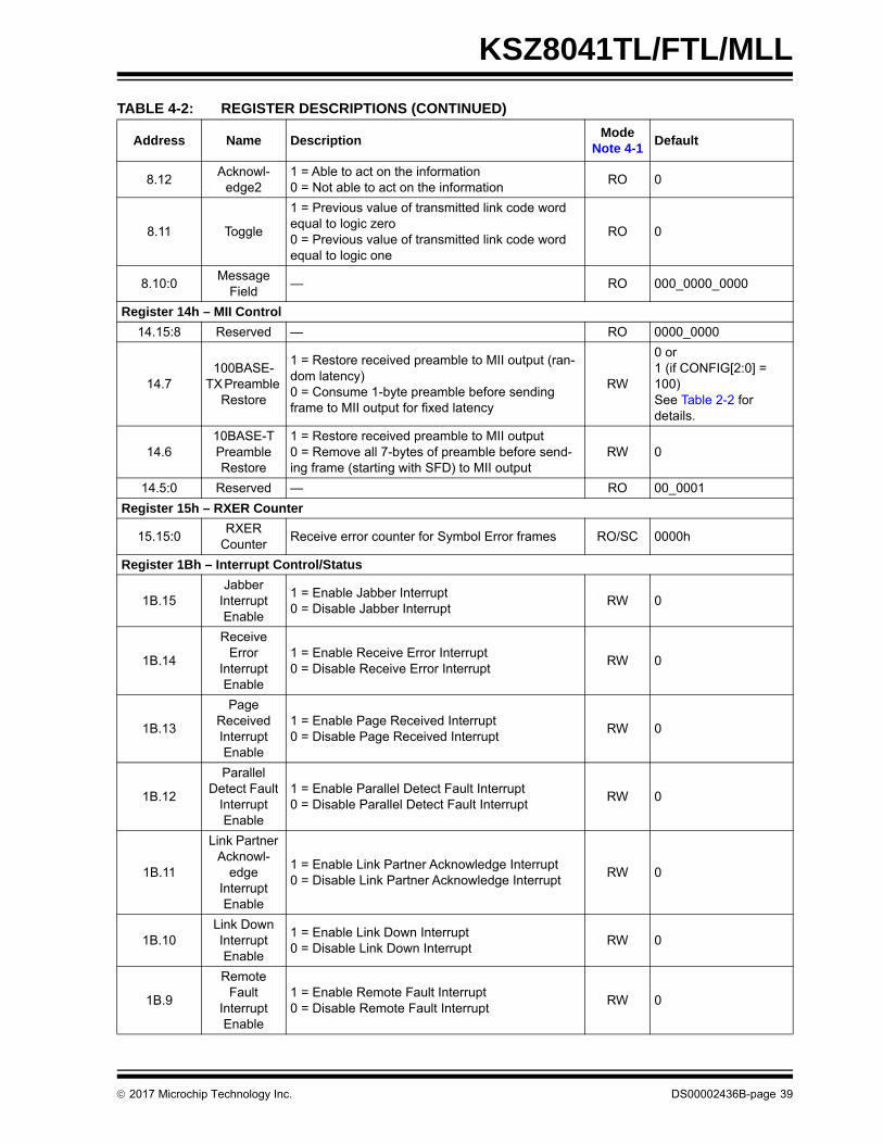
KSZ8041TL/FTL/MLL
8.12Acknowl-
edge21 = Able to act on the information0 = Not able to act on the information
RO 0
8.11 Toggle
1 = Previous value of transmitted link code word equal to logic zero0 = Previous value of transmitted link code word equal to logic one
RO 0
8.10:0Message
Field— RO 000_0000_0000
Register 14h – MII Control
14.15:8 Reserved — RO 0000_0000
14.7100BASE-
TX Preamble Restore
1 = Restore received preamble to MII output (ran-dom latency)0 = Consume 1-byte preamble before sending frame to MII output for fixed latency
RW
0 or1 (if CONFIG[2:0] = 100)See Table 2-2 for details.
14.610BASE-T Preamble Restore
1 = Restore received preamble to MII output0 = Remove all 7-bytes of preamble before send-ing frame (starting with SFD) to MII output
RW 0
14.5:0 Reserved — RO 00_0001
Register 15h – RXER Counter
15.15:0RXER
CounterReceive error counter for Symbol Error frames RO/SC 0000h
Register 1Bh – Interrupt Control/Status
1B.15Jabber
Interrupt Enable
1 = Enable Jabber Interrupt0 = Disable Jabber Interrupt
RW 0
1B.14
Receive Error
Interrupt Enable
1 = Enable Receive Error Interrupt0 = Disable Receive Error Interrupt
RW 0
1B.13
Page Received Interrupt Enable
1 = Enable Page Received Interrupt0 = Disable Page Received Interrupt
RW 0
1B.12
Parallel Detect Fault
Interrupt Enable
1 = Enable Parallel Detect Fault Interrupt0 = Disable Parallel Detect Fault Interrupt
RW 0
1B.11
Link Partner Acknowl-
edge Interrupt Enable
1 = Enable Link Partner Acknowledge Interrupt0 = Disable Link Partner Acknowledge Interrupt
RW 0
1B.10Link Down Interrupt Enable
1 = Enable Link Down Interrupt0 = Disable Link Down Interrupt
RW 0
1B.9
Remote Fault
Interrupt Enable
1 = Enable Remote Fault Interrupt0 = Disable Remote Fault Interrupt
RW 0
TABLE 4-2: REGISTER DESCRIPTIONS (CONTINUED)
Address Name DescriptionMode
Note 4-1Default
2017 Microchip Technology Inc. DS00002436B-page 39
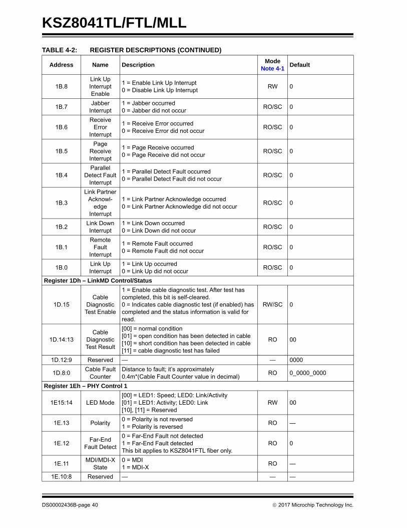
KSZ8041TL/FTL/MLL
1B.8Link Up Interrupt Enable
1 = Enable Link Up Interrupt0 = Disable Link Up Interrupt
RW 0
1B.7Jabber
Interrupt1 = Jabber occurred0 = Jabber did not occur
RO/SC 0
1B.6Receive
Error Interrupt
1 = Receive Error occurred0 = Receive Error did not occur
RO/SC 0
1B.5Page
Receive Interrupt
1 = Page Receive occurred0 = Page Receive did not occur
RO/SC 0
1B.4Parallel
Detect Fault Interrupt
1 = Parallel Detect Fault occurred0 = Parallel Detect Fault did not occur
RO/SC 0
1B.3
Link Partner Acknowl-
edge Interrupt
1 = Link Partner Acknowledge occurred0 = Link Partner Acknowledge did not occur
RO/SC 0
1B.2Link Down Interrupt
1 = Link Down occurred0 = Link Down did not occur
RO/SC 0
1B.1Remote
Fault Interrupt
1 = Remote Fault occurred0 = Remote Fault did not occur
RO/SC 0
1B.0Link Up Interrupt
1 = Link Up occurred0 = Link Up did not occur
RO/SC 0
Register 1Dh – LinkMD Control/Status
1D.15Cable
Diagnostic Test Enable
1 = Enable cable diagnostic test. After test has completed, this bit is self-cleared.0 = Indicates cable diagnostic test (if enabled) has completed and the status information is valid for read.
RW/SC 0
1D.14:13Cable
Diagnostic Test Result
[00] = normal condition[01] = open condition has been detected in cable[10] = short condition has been detected in cable[11] = cable diagnostic test has failed
RO 00
1D.12:9 Reserved — — 0000
1D.8:0Cable Fault
CounterDistance to fault; it’s approximately0.4m*(Cable Fault Counter value in decimal)
RO 0_0000_0000
Register 1Eh – PHY Control 1
1E15:14 LED Mode[00] = LED1: Speed; LED0: Link/Activity[01] = LED1: Activity; LED0: Link[10], [11] = Reserved
RW 00
1E.13 Polarity0 = Polarity is not reversed1 = Polarity is reversed
RO —
1E.12Far-End
Fault Detect
0 = Far-End Fault not detected1 = Far-End Fault detectedThis bit applies to KSZ8041FTL fiber only.
RO 0
1E.11MDI/MDI-X
State0 = MDI1 = MDI-X
RO —
1E.10:8 Reserved — — —
TABLE 4-2: REGISTER DESCRIPTIONS (CONTINUED)
Address Name DescriptionMode
Note 4-1Default
DS00002436B-page 40 2017 Microchip Technology Inc.
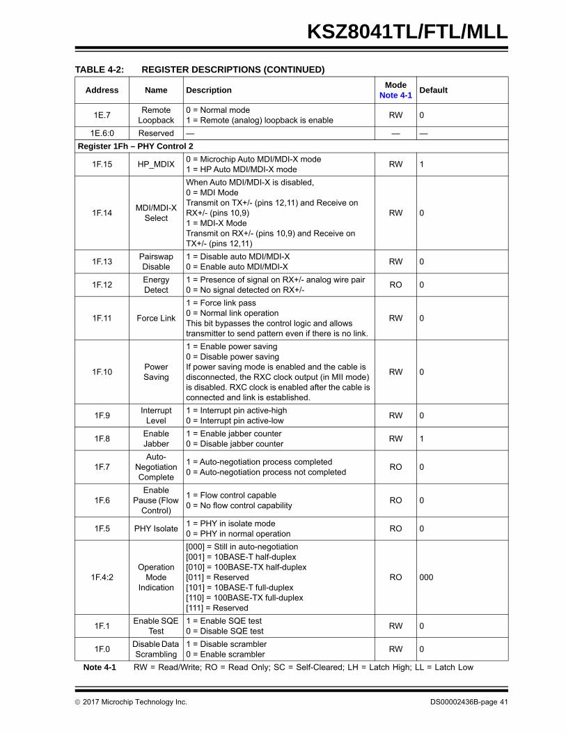
KSZ8041TL/FTL/MLL
Note 4-1 RW = Read/Write; RO = Read Only; SC = Self-Cleared; LH = Latch High; LL = Latch Low
1E.7Remote
Loopback0 = Normal mode1 = Remote (analog) loopback is enable
RW 0
1E.6:0 Reserved — — —
Register 1Fh – PHY Control 2
1F.15 HP_MDIX0 = Microchip Auto MDI/MDI-X mode1 = HP Auto MDI/MDI-X mode
RW 1
1F.14MDI/MDI-X
Select
When Auto MDI/MDI-X is disabled,0 = MDI ModeTransmit on TX+/- (pins 12,11) and Receive on RX+/- (pins 10,9)1 = MDI-X ModeTransmit on RX+/- (pins 10,9) and Receive on TX+/- (pins 12,11)
RW 0
1F.13Pairswap Disable
1 = Disable auto MDI/MDI-X0 = Enable auto MDI/MDI-X
RW 0
1F.12Energy Detect
1 = Presence of signal on RX+/- analog wire pair0 = No signal detected on RX+/-
RO 0
1F.11 Force Link
1 = Force link pass0 = Normal link operationThis bit bypasses the control logic and allows transmitter to send pattern even if there is no link.
RW 0
1F.10Power Saving
1 = Enable power saving 0 = Disable power savingIf power saving mode is enabled and the cable is disconnected, the RXC clock output (in MII mode) is disabled. RXC clock is enabled after the cable is connected and link is established.
RW 0
1F.9Interrupt
Level1 = Interrupt pin active-high0 = Interrupt pin active-low
RW 0
1F.8Enable Jabber
1 = Enable jabber counter0 = Disable jabber counter
RW 1
1F.7Auto-
Negotiation Complete
1 = Auto-negotiation process completed0 = Auto-negotiation process not completed
RO 0
1F.6Enable
Pause (Flow Control)
1 = Flow control capable0 = No flow control capability
RO 0
1F.5 PHY Isolate1 = PHY in isolate mode0 = PHY in normal operation
RO 0
1F.4:2Operation
Mode Indication
[000] = Still in auto-negotiation[001] = 10BASE-T half-duplex[010] = 100BASE-TX half-duplex[011] = Reserved[101] = 10BASE-T full-duplex[110] = 100BASE-TX full-duplex[111] = Reserved
RO 000
1F.1Enable SQE
Test1 = Enable SQE test0 = Disable SQE test
RW 0
1F.0Disable Data Scrambling
1 = Disable scrambler0 = Enable scrambler
RW 0
TABLE 4-2: REGISTER DESCRIPTIONS (CONTINUED)
Address Name DescriptionMode
Note 4-1Default
2017 Microchip Technology Inc. DS00002436B-page 41

KSZ8041TL/FTL/MLL
5.0 OPERATIONAL CHARACTERISTICS
5.1 Absolute Maximum Ratings*
Supply Voltage (VDD_1.8, VDDA_1.8, V1.8_OUT)........................................................................................... –0.5V to +2.4V
Supply Voltage (VDDIO_3.3, VDDA_3.3)........................................................................................................ –0.5V to +4.0V
Input Voltage (All Inputs) ........................................................................................................................... –0.5V to +4.0V
Output Voltage (All Outputs) ..................................................................................................................... –0.5V to +4.0V
Lead Temperature (soldering, 10s) .......................................................................................................................+260°C
Storage Temperature (TS) ......................................................................................................................–55°C to +150°C
*Exceeding the absolute maximum rating may damage the device. Stresses greater than the absolute maximum ratingmay cause permanent damage to the device. Operation of the device at these or any other conditions above those spec-ified in the operating sections of this specification is not implied. Maximum conditions for extended periods may affectreliability.
5.2 Operating Ratings**
Supply Voltage (VDDIO_3.3, VDDA_3.3)................................................................................................ +3.135V to +3.465V
Ambient Operating Temperature (TA) (Commercial)......................................................................................................................................0°C to +70°C
(Industrial) ......................................................................................................................................–40°C to +85°C
Maximum Junction Temperature (TJ) ....................................................................................................................+125°C
Thermal Resistance Junction-to-Ambient (ΘJA)............................................................................................................................. +69.64°C/W
Junction-to-Case (ΘJC) ...................................................................................................................................... +15°C/W
**The device is not guaranteed to function outside its operating ratings.
Note: Do not drive input signals without power supplied to the device.
DS00002436B-page 42 2017 Microchip Technology Inc.

KSZ8041TL/FTL/MLL
6.0 ELECTRICAL CHARACTERISTICS
TA = 25°C. Specification is for packaged product only.
Note 6-1 Current consumption is for the single 3.3V supply KSZ8041TL/FTL/MLL device only, and includes the1.8V supply voltage (VDD_1.8, VDDA_1.8, V1.8_OUT) that is provided by the KSZ8041TL/FTL/MLL. ThePHY port’s transformer consumes an additional 45 mA @ 3.3V for 100BASE-TX and 70 mA @ 3.3Vfor 10BASE-T.
TABLE 6-1: ELECTRICAL CHARACTERISTICS
Parameters Symbol Min. Typ. Max. Units Note
Supply Current (Note 6-1)
100BASE-TX IDD1 — 53.0 58.3 mAChip only (no transformer);
Full-duplex traffic @ 100% utilization
10BASE-T IDD2 — 38.0 41.8 mAChip only (no transformer);
Full-duplex traffic @ 100% utilization
Power Saving Mode IDD3 — 32.0 35.2 mAEthernet cable disconnected (reg.
1F.10 = 1)
Power Down Mode IDD4 — 4.0 4.4 mA Software power down (reg. 0.11 = 1)
CMOS Inputs
Input High Voltage VIH 2.0 — — V —
Input Low Voltage VIL — — 0.8 V —
Input Current IIN — –10 10 µA VIN = GND ~ VDDIO
CMOS Outputs
Output High Voltage VOH 2.4 — — V IOH = –4 mA
Output Low Voltage VOL — — 0.4 V IOL = 4 mA
Output Tri-State Leakage |IOZ| — — 10 µA —
LED Outputs
Output Drive Current ILED — 8 — mA Each LED pin (LED0, LED1)
100BASE-TX Transmit (measured differentially after 1:1 transformer)
Peak Differential Output Voltage
VO 0.95 — 1.05 V100Ω termination across differential
output
Output Voltage Imbalance VIMB — — 2 %100Ω termination across differential
output
Rise/Fall Time tr/tf 3 — 5 ns —
Rise/Fall Time Imbalance — 0 — 0.5 ns —
Duty Cycle Distortion — — — ±0.25 ns —
Overshoot — — — 5 % —
Reference Voltage of ISET VSET — 0.65 — V —
Output Jitter — — 0.7 1.4 ns Peak-to-Peak
10BASE-T Transmit (measured differentially after 1:1 transformer)
Peak Differential Output Voltage
VP 2.2 — 2.8 V100Ω termination across differential
output
Jitter Added — — — 3.5 ns Peak-to-Peak
Rise/Fall Time tr/tf — 25 — ns —
10BASE-T Receive
Squelch Threshold VSQ — 400 — mV 5 MHz square wave
2017 Microchip Technology Inc. DS00002436B-page 43

KSZ8041TL/FTL/MLL
7.0 TIMING SPECIFICATIONS
7.1 MII SQE Timing (10BASE-T)
FIGURE 7-1: MII SQE TIMING (10BASE-T)
TABLE 7-1: MII SQE TIMING (10BASE-T) PARAMETERS
Symbol Parameter Min. Typ. Max. Units
tP TXC period — 400 — ns
tWL TXC pulse width low — 200 — ns
tWH TXC pulse width high — 200 — ns
tSQE COL (SQE) delay after TXEN de-asserted — 2.5 — µs
tSQEP COL (SQE) pulse duration — 1.0 — µs
TXC
tSQECOL
tSQEP
TXEN
tWL
tWH
tP
DS00002436B-page 44 2017 Microchip Technology Inc.
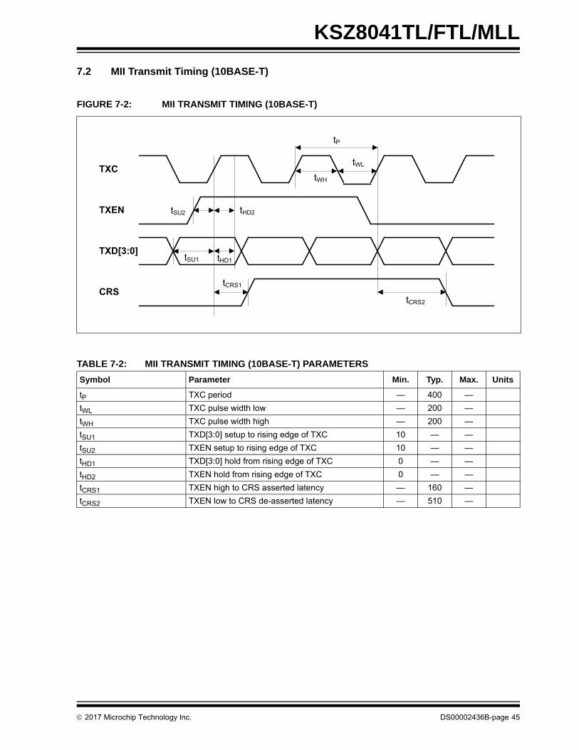
KSZ8041TL/FTL/MLL
7.2 MII Transmit Timing (10BASE-T)
FIGURE 7-2: MII TRANSMIT TIMING (10BASE-T)
TABLE 7-2: MII TRANSMIT TIMING (10BASE-T) PARAMETERS
Symbol Parameter Min. Typ. Max. Units
tP TXC period — 400 —
tWL TXC pulse width low — 200 —
tWH TXC pulse width high — 200 —
tSU1 TXD[3:0] setup to rising edge of TXC 10 — —
tSU2 TXEN setup to rising edge of TXC 10 — —
tHD1 TXD[3:0] hold from rising edge of TXC 0 — —
tHD2 TXEN hold from rising edge of TXC 0 — —
tCRS1 TXEN high to CRS asserted latency — 160 —
tCRS2 TXEN low to CRS de-asserted latency — 510 —
TXC
tHD2tSU2TXEN
TXD[3:0] tSU1 tHD1
CRStCRS2
tCRS1
tWH
tWL
tP
2017 Microchip Technology Inc. DS00002436B-page 45
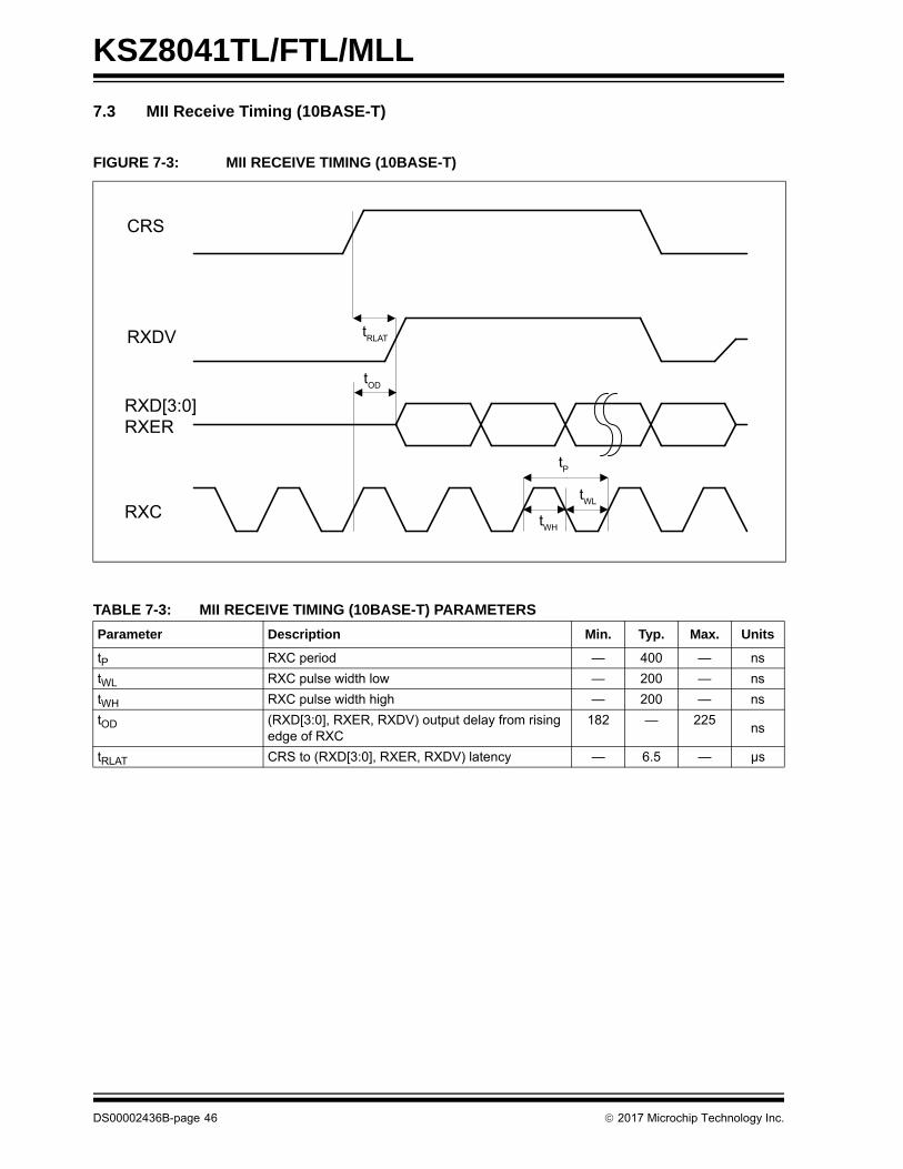
KSZ8041TL/FTL/MLL
7.3 MII Receive Timing (10BASE-T)
FIGURE 7-3: MII RECEIVE TIMING (10BASE-T)
TABLE 7-3: MII RECEIVE TIMING (10BASE-T) PARAMETERS
Parameter Description Min. Typ. Max. Units
tP RXC period — 400 — ns
tWL RXC pulse width low — 200 — ns
tWH RXC pulse width high — 200 — ns
tOD (RXD[3:0], RXER, RXDV) output delay from rising edge of RXC
182 — 225ns
tRLAT CRS to (RXD[3:0], RXER, RXDV) latency — 6.5 — µs
tWL
tWH
tP
tOD
CRS
RXDV
RXD[3:0]RXER
RXC
tRLAT
DS00002436B-page 46 2017 Microchip Technology Inc.
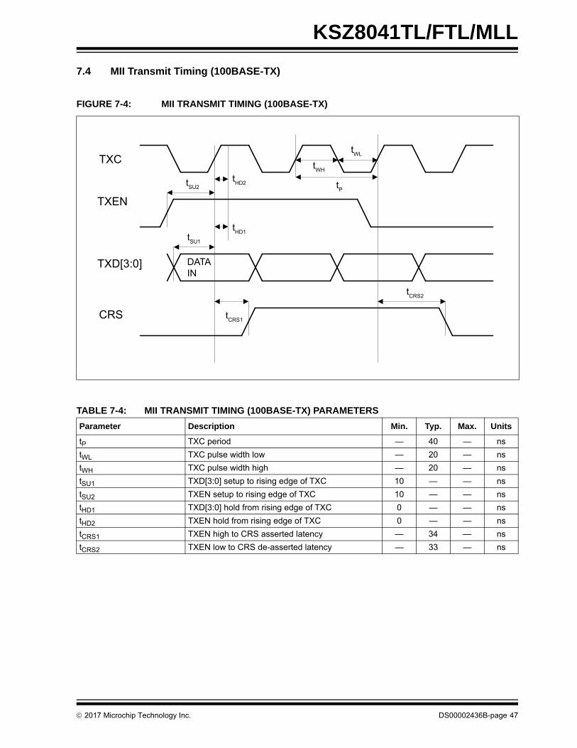
KSZ8041TL/FTL/MLL
7.4 MII Transmit Timing (100BASE-TX)
FIGURE 7-4: MII TRANSMIT TIMING (100BASE-TX)
TABLE 7-4: MII TRANSMIT TIMING (100BASE-TX) PARAMETERS
Parameter Description Min. Typ. Max. Units
tP TXC period — 40 — ns
tWL TXC pulse width low — 20 — ns
tWH TXC pulse width high — 20 — ns
tSU1 TXD[3:0] setup to rising edge of TXC 10 — — ns
tSU2 TXEN setup to rising edge of TXC 10 — — ns
tHD1 TXD[3:0] hold from rising edge of TXC 0 — — ns
tHD2 TXEN hold from rising edge of TXC 0 — — ns
tCRS1 TXEN high to CRS asserted latency — 34 — ns
tCRS2 TXEN low to CRS de-asserted latency — 33 — ns
TXC
TXEN
TXD[3:0]
CRS
DATAIN
tSU2tHD2
tSU1
tHD1
tP
tWH
tWL
tCRS1
tCRS2
2017 Microchip Technology Inc. DS00002436B-page 47
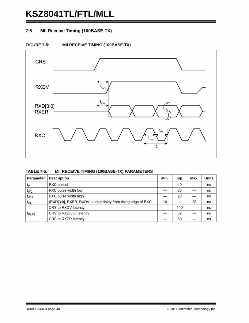
KSZ8041TL/FTL/MLL
7.5 MII Receive Timing (100BASE-TX)
FIGURE 7-5: MII RECEIVE TIMING (100BASE-TX)
TABLE 7-5: MII RECEIVE TIMING (100BASE-TX) PARAMETERS
Parameter Description Min. Typ. Max. Units
tP RXC period — 40 — ns
tWL RXC pulse width low — 20 — ns
tWH RXC pulse width high — 20 — ns
tOD (RXD[3:0], RXER, RXDV) output delay from rising edge of RXC 19 — 25 ns
tRLAT
CRS to RXDV latency — 140 — ns
CRS to RXD[3:0] latency — 52 — ns
CRS to RXER latency — 60 — ns
tWL
tWH
tP
tOD
CRS
RXDV
RXD[3:0]RXER
RXC
tRLAT
DS00002436B-page 48 2017 Microchip Technology Inc.
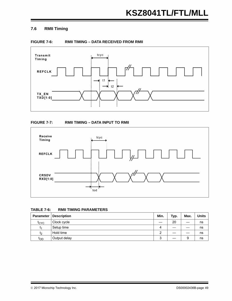
KSZ8041TL/FTL/MLL
7.6 RMII Timing
FIGURE 7-6: RMII TIMING – DATA RECEIVED FROM RMII
FIGURE 7-7: RMII TIMING – DATA INPUT TO RMII
TABLE 7-6: RMII TIMING PARAMETERS
Parameter Description Min. Typ. Max. Units
tCYC Clock cycle — 20 — ns
t1 Setup time 4 — — ns
t2 Hold time 2 — — ns
tOD Output delay 3 — 9 ns
R EFCLK
tcyc
TX _ENTXD [1:0]
t1
t2
Transm itTim ing
REFCLK
tcyc
tod
CRSDVRXD[1:0]
ReceiveTiming
2017 Microchip Technology Inc. DS00002436B-page 49
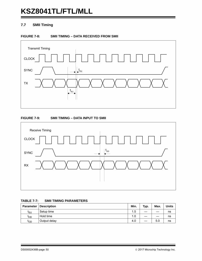
KSZ8041TL/FTL/MLL
7.7 SMII Timing
FIGURE 7-8: SMII TIMING – DATA RECEIVED FROM SMII
FIGURE 7-9: SMII TIMING – DATA INPUT TO SMII
TABLE 7-7: SMII TIMING PARAMETERS
Parameter Description Min. Typ. Max. Units
tSU Setup time 1.5 — — ns
tHD Hold time 1.0 — — ns
tOD Output delay 4.0 — 5.0 ns
Transmit Timing
CLOCK
SYNC
TX
tHU
tSU
Receive Timing
CLOCK
SYNC
RX
tOD
DS00002436B-page 50 2017 Microchip Technology Inc.

KSZ8041TL/FTL/MLL
7.8 Auto-Negotiation Timing
FIGURE 7-10: AUTO-NEGOTIATION FAST LINK PULSE (FLP) TIMING
TABLE 7-8: AUTO-NEGOTIATION FAST LINK PULSE TIMING PARAMETERS
Parameter Description Min. Typ. Max. Units
tBTB FLP Burst to FLP Burst 8 16 24 ms
tFLPW FLP Burst Width — 2 — ms
tPW Clock/Data Pulse Width — 100 — ns
tCTD Clock Pulse to Data Pulse 55.5 64 69.5 µs
tCTC Clock Pulse to Clock Pulse 111 128 139 µs
— Number of Clock/Data Pulses per FLP Burst 17 — 33 —
Auto-NegotiationFast Link Pulse (FLP) Tim ing
tFLPW
tBTB
TX+/TX-
FLP Burst
FLP Burst
tPWTX+/TX-
ClockPulse
DataPulse
ClockPulse
tPW
tCTD
tCTC
DataPulse
2017 Microchip Technology Inc. DS00002436B-page 51

KSZ8041TL/FTL/MLL
7.9 MDC/MDIO Timing
FIGURE 7-11: MDC/MDIO TIMING
TABLE 7-9: MDC/MDIO TIMING PARAMETERS
Parameter Description Min. Typ. Max. Units
tP MDC period — 400 — ns
tMD1 MDIO (PHY input) setup to rising edge of MDC 10 — — ns
tMD2 MDIO (PHY input) hold from rising edge of MDC 4 — — ns
tMD3 MDIO (PHY output) delay from rising edge of MDC — 222 — ns
tMD1
ValidData
MDIO(PHY input)
ValidData
MDC
tMD2
MDIO(PHY output)
ValidData
tMD3
tP
DS00002436B-page 52 2017 Microchip Technology Inc.
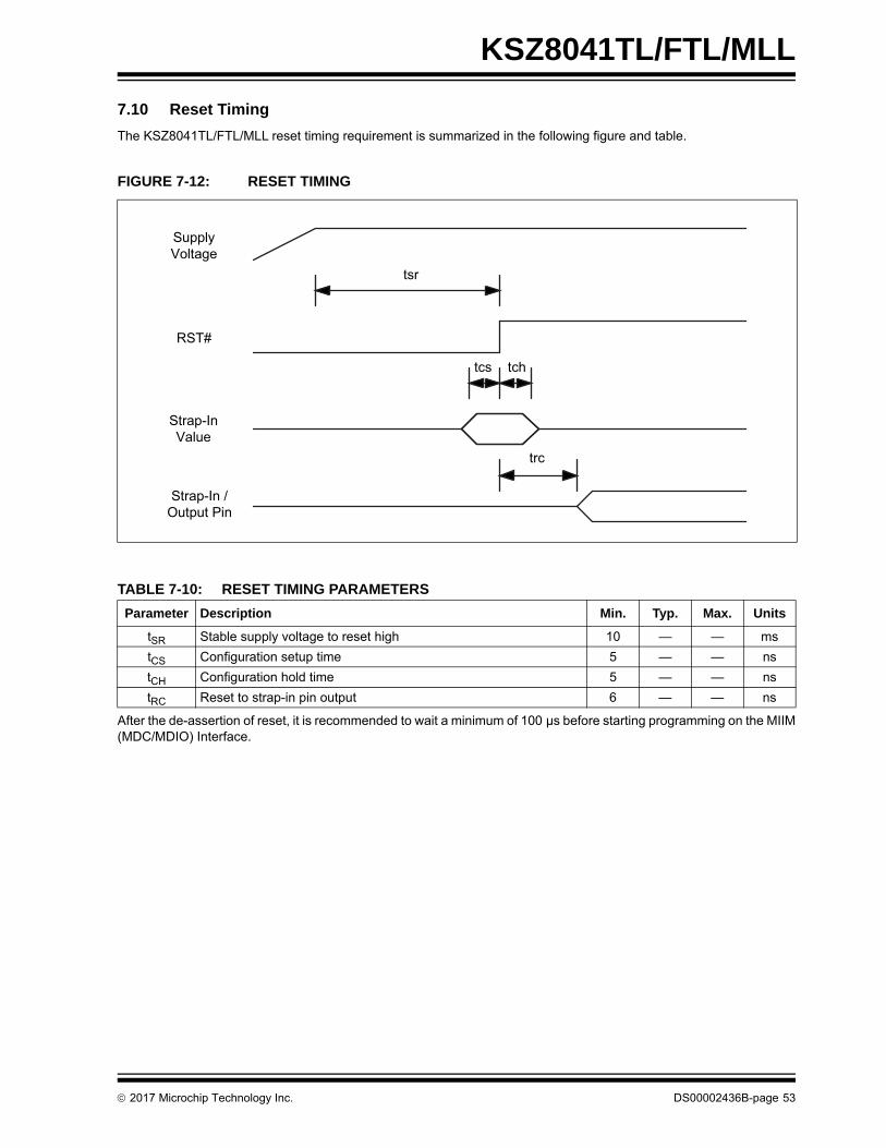
KSZ8041TL/FTL/MLL
7.10 Reset Timing
The KSZ8041TL/FTL/MLL reset timing requirement is summarized in the following figure and table.
After the de-assertion of reset, it is recommended to wait a minimum of 100 µs before starting programming on the MIIM(MDC/MDIO) Interface.
FIGURE 7-12: RESET TIMING
TABLE 7-10: RESET TIMING PARAMETERS
Parameter Description Min. Typ. Max. Units
tSR Stable supply voltage to reset high 10 — — ms
tCS Configuration setup time 5 — — ns
tCH Configuration hold time 5 — — ns
tRC Reset to strap-in pin output 6 — — ns
tsr
tcs tch
trc
Supply Voltage
RST#
Strap-In Value
Strap-In /Output Pin
2017 Microchip Technology Inc. DS00002436B-page 53
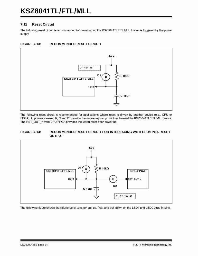
KSZ8041TL/FTL/MLL
7.11 Reset Circuit
The following reset circuit is recommended for powering up the KSZ8041TL/FTL/MLL if reset is triggered by the powersupply.
The following reset circuit is recommended for applications where reset is driven by another device (e.g., CPU orFPGA). At power-on-reset, R, C and D1 provide the necessary ramp rise time to reset the KSZ8041TL/FTL/MLL device.The RST_OUT_n from CPU/FPGA provides the warm reset after power up.
The following figure shows the reference circuits for pull-up, float and pull-down on the LED1 and LED0 strap-in pins.
FIGURE 7-13: RECOMMENDED RESET CIRCUIT
FIGURE 7-14: RECOMMENDED RESET CIRCUIT FOR INTERFACING WITH CPU/FPGA RESET OUTPUT
KSZ8041TL/FTL/MLL
3.3V
D1
D1: 1N4148
R 10
C 10μF
RST#
KSZ8041TL/FTL/MLL CPU/FPGA
3.3V
C 10μF
R 10
RST_OUT_n
D1
D2
D1, D2: 1N4148
RST#
DS00002436B-page 54 2017 Microchip Technology Inc.
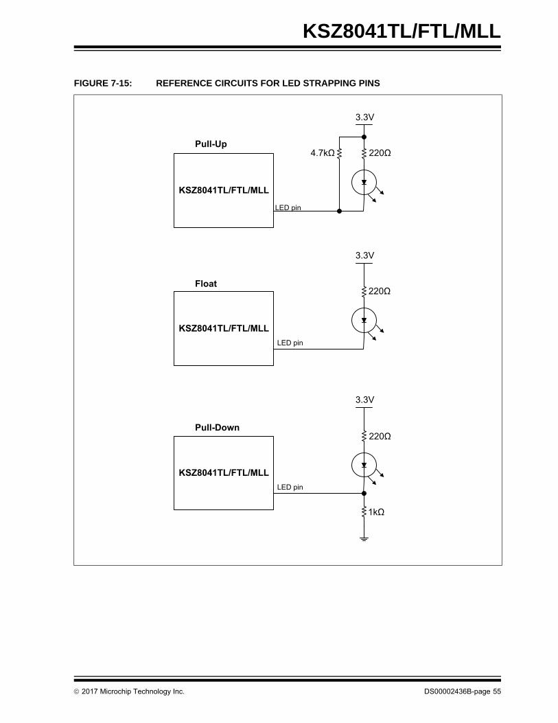
KSZ8041TL/FTL/MLL
FIGURE 7-15: REFERENCE CIRCUITS FOR LED STRAPPING PINS
LED pin
3.3V
Pull-Up
KSZ8041TL/FTL/MLL
3.3V
Float
KSZ8041TL/FTL/MLL
LED pin
3.3V
Pull-Down
KSZ8041TL/FTL/MLL
LED pin
2017 Microchip Technology Inc. DS00002436B-page 55

KSZ8041TL/FTL/MLL
8.0 SELECTION OF ISOLATION TRANSFORMERS
A 1:1 isolation transformer is required at the line interface. An isolation transformer with integrated common-mode chokeis recommended for exceeding FCC requirements.
Table 8-1 lists recommended transformer characteristics.
TABLE 8-1: TRANSFORMER SELECTION CRITERIA
Parameter Value Test Conditions
Turns Ratio 1 CT:1 CT —
Open-Circuit Inductance (min.) 350 µH 100 mV, 100 kHz, 8 mA
Leakage Inductance (max.) 0.4 µH 1 MHz (min.)
Interwinding Capacitance (max.) 12 pF —
D.C. Resistance (max.) 0.9Ω —
Insertion Loss (max.) –1.0 dB 0 MHz to 65 MHz
HIPOT (min.) 1500 VRMS —
TABLE 8-2: QUALIFIED SINGLE-PORT MAGNETICS
Manufacturer Part Number Auto MDI-X
Bel Fuse S558-5999-U7 Yes
Bel Fuse (Mag Jack) SI-46001 Yes
Bel Fuse (Mag Jack) SI-50170 Yes
Delta LF8505 Yes
LanKom LF-H41S Yes
Pulse H1102 Yes
Pulse (low cost) H1260 Yes
Transpower HB726
TDK (Mag Jack) TLA-6T718
TABLE 8-3: TYPICAL REFERENCE CRYSTAL CHARACTERISTICS
Characteristic Value
Frequency 25 MHz
Frequency Tolerance (max.) ±50 ppm
Load Capacitance (max.) 20 pF
Series Resistance 40Ω
DS00002436B-page 56 2017 Microchip Technology Inc.
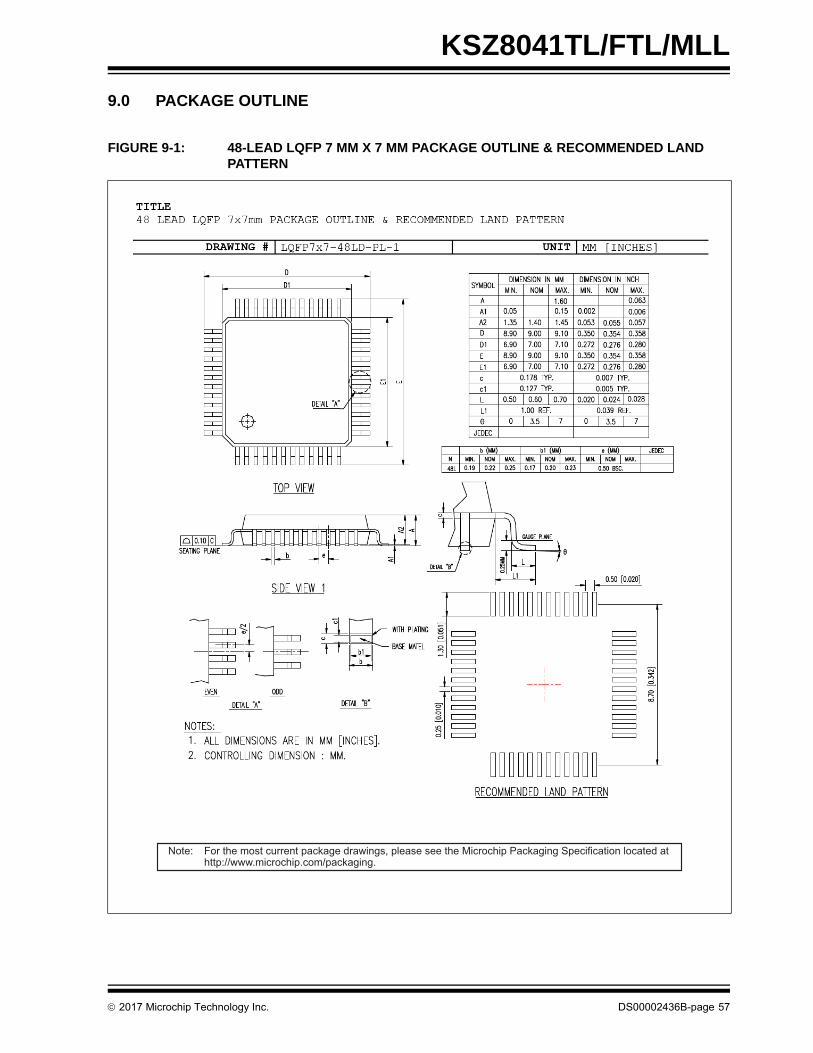
KSZ8041TL/FTL/MLL
9.0 PACKAGE OUTLINE
FIGURE 9-1: 48-LEAD LQFP 7 MM X 7 MM PACKAGE OUTLINE & RECOMMENDED LAND PATTERN
Note: For the most current package drawings, please see the Microchip Packaging Specification located at http://www.microchip.com/packaging.
2017 Microchip Technology Inc. DS00002436B-page 57
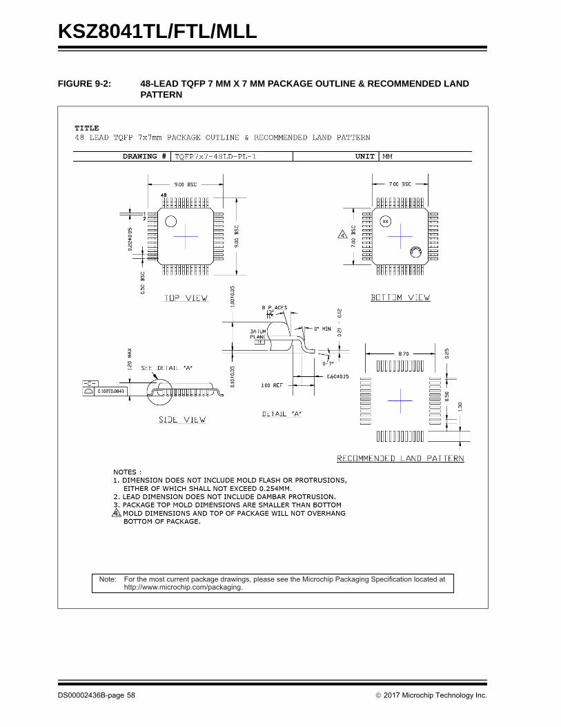
KSZ8041TL/FTL/MLL
FIGURE 9-2: 48-LEAD TQFP 7 MM X 7 MM PACKAGE OUTLINE & RECOMMENDED LAND PATTERN
Note: For the most current package drawings, please see the Microchip Packaging Specification located at http://www.microchip.com/packaging.
DS00002436B-page 58 2017 Microchip Technology Inc.

2017 Microchip Technology Inc. DS00002436B-page 59
KSZ8041TL/FTL/MLL
APPENDIX A: DATA SHEET REVISION HISTORY
TABLE A-1: REVISION HISTORY
Revision Section/Figure/Entry Correction
DS00002436B (10-04-17) Section 5.0, Operational Characteristics
Moved Maximum Junction Temperature information from Section 5.1, Absolute Maximum Ratings* to Section 5.2, Operating Ratings** for consistency with previous releases.
Rev. A (7-11-17) __ Converted Micrel data sheet KSZ8041TL/FTL/MLL to Microchip DS00002436B. Minor text changes throughout.
KSZ8041TL/FTL/MLL
DS00002436B-page 60 2017 Microchip Technology Inc.
THE MICROCHIP WEB SITE
Microchip provides online support via our WWW site at www.microchip.com. This web site is used as a means to makefiles and information easily available to customers. Accessible by using your favorite Internet browser, the web site con-tains the following information:
• Product Support – Data sheets and errata, application notes and sample programs, design resources, user’s guides and hardware support documents, latest software releases and archived software
• General Technical Support – Frequently Asked Questions (FAQ), technical support requests, online discussion groups, Microchip consultant program member listing
• Business of Microchip – Product selector and ordering guides, latest Microchip press releases, listing of semi-nars and events, listings of Microchip sales offices, distributors and factory representatives
CUSTOMER CHANGE NOTIFICATION SERVICE
Microchip’s customer notification service helps keep customers current on Microchip products. Subscribers will receivee-mail notification whenever there are changes, updates, revisions or errata related to a specified product family ordevelopment tool of interest.
To register, access the Microchip web site at www.microchip.com. Under “Support”, click on “Customer Change Notifi-cation” and follow the registration instructions.
CUSTOMER SUPPORT
Users of Microchip products can receive assistance through several channels:
• Distributor or Representative
• Local Sales Office
• Field Application Engineer (FAE)
• Technical Support
Customers should contact their distributor, representative or field application engineer (FAE) for support. Local salesoffices are also available to help customers. A listing of sales offices and locations is included in the back of this docu-ment.
Technical support is available through the web site at: http://microchip.com/support
2017 Microchip Technology Inc. DS00002436B-page 61
KSZ8041TL/FTL/MLL
PRODUCT IDENTIFICATION SYSTEM
To order or obtain information, e.g., on pricing or delivery, refer to the factory or the listed sales office.
Device: KSZ8041
Interface: M = MII Interface<blank> = MII/RMII InterfaceF = MII/RMII Interface with 100BASE-FX Fiber
Package: L = 48-Lead LQFPT = 48-Lead TQFP
Power Option: L = Integrated LDO/LDO Controller/Regulator
Temperature: <blank> = 0C to +70C (Commercial)I = –40C to +85C (Industrial)
Media Type: <blank> = 250/TrayTR = 1,000/ReelS = Serial MII Interface, 250/Tray, Commercial Temp. Only, KSZ8041TL/FTL Only
Examples:
a) KSZ8041MLL: MII Interface, 48-Lead LQFP,Integrated LDO, Commercial Temperature, 250/Tray
b) KSZ8041MLLI: MII Interface, 48-Lead LQFP,Integrated LDO, Industrial Temperature, 250/Tray
c) KSZ8041MLL-TR: MII Interface, 48-Lead LQFP,Integrated LDO, Commercial Temperature, 1,000/Reel
d) KSZ8041MLLI-TR: MII Interface, 48-Lead LQFP,Integrated LDO, Industrial Temperature, 1,000/Reel
e) KSZ8041TL: MII/RMII Interface, 48-Lead TQFP, Integrated LDO, Commercial Temperature, 250/Tray
f) KSZ8041TLI-S: Serial MII Interface, 48-LeadTQFP, Integrated LDO, Industrial Temperature, 250/Tray
g) KSZ8041FTL-TR: MII/RMII Interface with 100BASE-TX Fiber, 48-LeadTQFP, Integrated LDO, Commercial Temperature,1,000/Reel
h) KSZ8041FTLI: MII/RMII Interface with 100BASE-TX Fiber, 48-LeadTQFP, Integrated LDO, Industrial Temperature, 250/Tray
i) KSZ8041TL-TR: MII/RMII Interface, 48-Lead TQFP, Integrated LDO, Commercial Temperature, 1,000/Reel
j) KSZ8041FTL-S: Serial MII Interface, 48-LeadTQFP, Integrated LDO,Commercial Temperature,250/Tray
k) KSZ8041TLI: MII/RMII Interface, 48-Lead TQFP, Integrated LDO, Industrial Temperature, 250/Tray
l) KSZ8041FTL: MII/RMII Interface with 100BASE-TX Fiber, 48-LeadTQFP, Integrated LDO, Commercial Temperature, 250/Tray
PART NO. X X
PackageInterfaceDevice
X
Temperature
X
PowerOption
XX
MediaType
KSZ8041TL/FTL/MLL
DS
Note the following details of the code protection feature on Microchip devices:
• Microchip products meet the specification contained in their particular Microchip Data Sheet.
• Microchip believes that its family of products is one of the most secure families of its kind on the market today, when used in the intended manner and under normal conditions.
• There are dishonest and possibly illegal methods used to breach the code protection feature. All of these methods, to our knowledge, require using the Microchip products in a manner outside the operating specifications contained in Microchip’s Data Sheets. Most likely, the person doing so is engaged in theft of intellectual property.
• Microchip is willing to work with the customer who is concerned about the integrity of their code.
• Neither Microchip nor any other semiconductor manufacturer can guarantee the security of their code. Code protection does not mean that we are guaranteeing the product as “unbreakable.”
Code protection is constantly evolving. We at Microchip are committed to continuously improving the code protection features of ourproducts. Attempts to break Microchip’s code protection feature may be a violation of the Digital Millennium Copyright Act. If such actsallow unauthorized access to your software or other copyrighted work, you may have a right to sue for relief under that Act.
Information contained in this publication regarding device applications and the like is provided only for your convenience and may besuperseded by updates. It is your responsibility to ensure that your application meets with your specifications. MICROCHIP MAKES NOREPRESENTATIONS OR WARRANTIES OF ANY KIND WHETHER EXPRESS OR IMPLIED, WRITTEN OR ORAL, STATUTORY OROTHERWISE, RELATED TO THE INFORMATION, INCLUDING BUT NOT LIMITED TO ITS CONDITION, QUALITY, PERFORMANCE,MERCHANTABILITY OR FITNESS FOR PURPOSE. Microchip disclaims all liability arising from this information and its use. Use of Micro-chip devices in life support and/or safety applications is entirely at the buyer’s risk, and the buyer agrees to defend, indemnify and holdharmless Microchip from any and all damages, claims, suits, or expenses resulting from such use. No licenses are conveyed, implicitly orotherwise, under any Microchip intellectual property rights unless otherwise stated.
Trademarks
The Microchip name and logo, the Microchip logo, AnyRate, AVR, AVR logo, AVR Freaks, BeaconThings, BitCloud, CryptoMemory, CryptoRF, dsPIC, FlashFlex, flexPWR, Heldo, JukeBlox, KEELOQ, KEELOQ logo, Kleer, LANCheck, LINK MD, maXStylus, maXTouch, MediaLB, megaAVR, MOST, MOST logo, MPLAB, OptoLyzer, PIC, picoPower, PICSTART, PIC32 logo, Prochip Designer, QTouch, RightTouch, SAM-BA, SpyNIC, SST, SST Logo, SuperFlash, tinyAVR, UNI/O, and XMEGA are registered trademarks of Microchip Technology Incorporated in the U.S.A. and other countries.
ClockWorks, The Embedded Control Solutions Company, EtherSynch, Hyper Speed Control, HyperLight Load, IntelliMOS, mTouch, Precision Edge, and Quiet-Wire are registered trademarks of Microchip Technology Incorporated in the U.S.A.
Adjacent Key Suppression, AKS, Analog-for-the-Digital Age, Any Capacitor, AnyIn, AnyOut, BodyCom, chipKIT, chipKIT logo, CodeGuard, CryptoAuthentication, CryptoCompanion, CryptoController, dsPICDEM, dsPICDEM.net, Dynamic Average Matching, DAM, ECAN, EtherGREEN, In-Circuit Serial Programming, ICSP, Inter-Chip Connectivity, JitterBlocker, KleerNet, KleerNet logo, Mindi, MiWi, motorBench, MPASM, MPF, MPLAB Certified logo, MPLIB, MPLINK, MultiTRAK, NetDetach, Omniscient Code Generation, PICDEM, PICDEM.net, PICkit, PICtail, PureSilicon, QMatrix, RightTouch logo, REAL ICE, Ripple Blocker, SAM-ICE, Serial Quad I/O, SMART-I.S., SQI, SuperSwitcher, SuperSwitcher II, Total Endurance, TSHARC, USBCheck, VariSense, ViewSpan, WiperLock, Wireless DNA, and ZENA are trademarks of Microchip Technology Incorporated in the U.S.A. and other countries.
SQTP is a service mark of Microchip Technology Incorporated in the U.S.A.
Silicon Storage Technology is a registered trademark of Microchip Technology Inc. in other countries.
GestIC is a registered trademark of Microchip Technology Germany II GmbH & Co. KG, a subsidiary of Microchip Technology Inc., in other countries.
All other trademarks mentioned herein are property of their respective companies.
© 2017, Microchip Technology Incorporated, All Rights Reserved.
ISBN: 9781522422136
00002436B-page 62 2017 Microchip Technology Inc.
Microchip received ISO/TS-16949:2009 certification for its worldwide headquarters, design and wafer fabrication facilities in Chandler and Tempe, Arizona; Gresham, Oregon and design centers in California and India. The Company’s quality system processes and procedures are for its PIC® MCUs and dsPIC® DSCs, KEELOQ® code hopping devices, Serial EEPROMs, microperipherals, nonvolatile memory and analog products. In addition, Microchip’s quality system for the design and manufacture of development systems is ISO 9001:2000 certified.
QUALITYMANAGEMENTSYSTEMCERTIFIEDBYDNV
== ISO/TS16949==

DS00002436B-page 63 2017 Microchip Technology Inc.
AMERICASCorporate Office2355 West Chandler Blvd.Chandler, AZ 85224-6199Tel: 480-792-7200 Fax: 480-792-7277Technical Support: http://www.microchip.com/supportWeb Address: www.microchip.com
AtlantaDuluth, GA Tel: 678-957-9614 Fax: 678-957-1455
Austin, TXTel: 512-257-3370
BostonWestborough, MA Tel: 774-760-0087 Fax: 774-760-0088
ChicagoItasca, IL Tel: 630-285-0071 Fax: 630-285-0075
DallasAddison, TX Tel: 972-818-7423 Fax: 972-818-2924
DetroitNovi, MI Tel: 248-848-4000
Houston, TX Tel: 281-894-5983
IndianapolisNoblesville, IN Tel: 317-773-8323Fax: 317-773-5453Tel: 317-536-2380
Los AngelesMission Viejo, CA Tel: 949-462-9523Fax: 949-462-9608Tel: 951-273-7800
Raleigh, NC Tel: 919-844-7510
New York, NY Tel: 631-435-6000
San Jose, CA Tel: 408-735-9110Tel: 408-436-4270
Canada - TorontoTel: 905-695-1980 Fax: 905-695-2078
ASIA/PACIFICAsia Pacific OfficeSuites 3707-14, 37th FloorTower 6, The GatewayHarbour City, Kowloon
Hong KongTel: 852-2943-5100Fax: 852-2401-3431
Australia - SydneyTel: 61-2-9868-6733Fax: 61-2-9868-6755
China - BeijingTel: 86-10-8569-7000 Fax: 86-10-8528-2104
China - ChengduTel: 86-28-8665-5511Fax: 86-28-8665-7889
China - ChongqingTel: 86-23-8980-9588Fax: 86-23-8980-9500
China - DongguanTel: 86-769-8702-9880
China - GuangzhouTel: 86-20-8755-8029
China - HangzhouTel: 86-571-8792-8115 Fax: 86-571-8792-8116
China - Hong Kong SARTel: 852-2943-5100 Fax: 852-2401-3431
China - NanjingTel: 86-25-8473-2460Fax: 86-25-8473-2470
China - QingdaoTel: 86-532-8502-7355Fax: 86-532-8502-7205
China - ShanghaiTel: 86-21-3326-8000 Fax: 86-21-3326-8021
China - ShenyangTel: 86-24-2334-2829Fax: 86-24-2334-2393
China - ShenzhenTel: 86-755-8864-2200 Fax: 86-755-8203-1760
China - WuhanTel: 86-27-5980-5300Fax: 86-27-5980-5118
China - XianTel: 86-29-8833-7252Fax: 86-29-8833-7256
ASIA/PACIFICChina - XiamenTel: 86-592-2388138 Fax: 86-592-2388130
China - ZhuhaiTel: 86-756-3210040 Fax: 86-756-3210049
India - BangaloreTel: 91-80-3090-4444 Fax: 91-80-3090-4123
India - New DelhiTel: 91-11-4160-8631Fax: 91-11-4160-8632
India - PuneTel: 91-20-3019-1500
Japan - OsakaTel: 81-6-6152-7160 Fax: 81-6-6152-9310
Japan - TokyoTel: 81-3-6880- 3770 Fax: 81-3-6880-3771
Korea - DaeguTel: 82-53-744-4301Fax: 82-53-744-4302
Korea - SeoulTel: 82-2-554-7200Fax: 82-2-558-5932 or 82-2-558-5934
Malaysia - Kuala LumpurTel: 60-3-6201-9857Fax: 60-3-6201-9859
Malaysia - PenangTel: 60-4-227-8870Fax: 60-4-227-4068
Philippines - ManilaTel: 63-2-634-9065Fax: 63-2-634-9069
SingaporeTel: 65-6334-8870Fax: 65-6334-8850
Taiwan - Hsin ChuTel: 886-3-5778-366Fax: 886-3-5770-955
Taiwan - KaohsiungTel: 886-7-213-7830
Taiwan - TaipeiTel: 886-2-2508-8600 Fax: 886-2-2508-0102
Thailand - BangkokTel: 66-2-694-1351Fax: 66-2-694-1350
EUROPEAustria - WelsTel: 43-7242-2244-39Fax: 43-7242-2244-393
Denmark - CopenhagenTel: 45-4450-2828 Fax: 45-4485-2829
Finland - EspooTel: 358-9-4520-820
France - ParisTel: 33-1-69-53-63-20 Fax: 33-1-69-30-90-79
France - Saint CloudTel: 33-1-30-60-70-00
Germany - GarchingTel: 49-8931-9700Germany - HaanTel: 49-2129-3766400
Germany - HeilbronnTel: 49-7131-67-3636
Germany - KarlsruheTel: 49-721-625370
Germany - MunichTel: 49-89-627-144-0 Fax: 49-89-627-144-44
Germany - RosenheimTel: 49-8031-354-560
Israel - Ra’anana Tel: 972-9-744-7705
Italy - Milan Tel: 39-0331-742611 Fax: 39-0331-466781
Italy - PadovaTel: 39-049-7625286
Netherlands - DrunenTel: 31-416-690399 Fax: 31-416-690340
Norway - TrondheimTel: 47-7289-7561
Poland - WarsawTel: 48-22-3325737
Romania - BucharestTel: 40-21-407-87-50
Spain - MadridTel: 34-91-708-08-90Fax: 34-91-708-08-91
Sweden - GothenbergTel: 46-31-704-60-40
Sweden - StockholmTel: 46-8-5090-4654
UK - WokinghamTel: 44-118-921-5800Fax: 44-118-921-5820
Worldwide Sales and Service
11/07/16

![Radio Frequency and Smart Meters · 2020. 8. 19. · *LSS7OVUL¶H[LHY 4PJYV^H]L6]LU¶ MLL[:THY[4L[LY¶ MLL[:THY[4L[LY¶ MLL[>P-P9V\[LY¶ MLL[-49HKPV ;=)YVHKJHZ[4H_PT\T 4PUPT\T Radio](https://img.pdfslide.us/doc/110x75/608bf4d4df473b5faf773b64/radio-frequency-and-smart-meters-2020-8-19-lss7ovulhlhy-4pjyvhl6lu.jpg)