Embed Size (px)
Citation preview

EasyChair Preprint 6235
Kelvin Bridge Structure Based TSV Test forWeak Faults
Hao Chang, Zhengfeng Huang and Tianming Ni
EasyChair preprints are intended for rapiddissemination of research results and areintegrated with the rest of EasyChair.
August 5, 2021

Kelvin Bridge Structure Based TSV Test for Weak Faults
Hao ChangSchool of Management Science and Engineering
Anhui University of Finance & EconomicsNo. 962, Caoshan Road, Bengbu, Anhui, China, 233030
Zhengfeng Huang, Tianming NiSchool of Microelectronics
Hefei University of TechnologyNo. 193, Tunxi Road, Hefei, China, 230009
[email protected], [email protected]
Abstract—Due to the immaturity of manufacturing process,TSV is vulnerable to a variety of defects, which brings new testingchallenges. Most of the existing test methods are suffer from thetest resolution and difficult to detect weak faults. Borrowing thewisdom of Kelvin Bridge, a non-invasive test method is proposedto detect resistive open fault and leakage fault. By adjustingthe resistances on the bridge arm to make them change in equalproportion, the adverse effects of contact resistance and parasiticresistance on the wire can be eliminated. HSPICE simulationusing 45 nm CMOS technology show that it can successfullydetect resistive open fault above 0.1 Ω and leakage fault below10 MΩ. The effectiveness of the test scheme is further provedby process-voltage-temperature (PVT) analysis.
Keywords—Three dimensional integrated circuits (3D ICs),through silicon vias (TSVs), Kelvin Bridge, resistive open fault,leakage fault.
I. INTRODUCTION
TSVs are crucial components used for signal transmission,power supply, and fault tolerance between 3D ICs layers, butalso susceptible to manufacturing defects[1]. In the manufac-turing process, narrow and deep holes are first etched on thesilicon wafer, then the isolation material is filled, and finallythe copper is poured. Due to the imperfection of manufacturingprocess, defects will result in new testing challenges.
The research of TSVs testing technology is helpful todetect faults caused by physical defects in a TSV, so as toimprove the yield and reliability of 3D ICs. At present, thereare two kinds of representative methods in the research ofTSV test: 1) probe based TSV test[2][3][4]; 2) built-in self-test (BIST) based TSV test[5][6][7].
An early method for testing TSVs directly with probes isproposed in [2]. Many single probe needle tips are utilized tocontact with multiple TSVs and form a single network, whichsolves the problem of mismatch between TSV pitch and tipsize. For a TSV with nominal value of 20 fF , the direct mea-surement result of probe method is 20.25 fF , which is veryclose to the actual value. A Micro-Electromechanical Systemsbased TSV probing technique is proposed to pinpoint the faultto a specific defective TSV without affecting their integrity[3].Finite Element Analysis tool is utilized to analyze the stresson TSV pads. An efficient binary search-based algorithm ispresented to guide the probe card movement and diagnose thefaulty TSVs [4]. The mathematical analysis shows that the testefficiency can be greatly improved by choosing proper probeneedles, and by adjusting iterative algorithm according to thefault distribution of TSVs. Generally, the advantage of theprobe test method lies in its high test accuracy, but the mainproblem is the difficulty in test access, which is embodied in:1) It brings additional burden to the test equipment, such as
customizing and activating the probe card. 2) The probe testneeds to contact the back of the wafer after thinning, whichis difficult to implement in practice. 3) The contact force onthe tip of TSV or solder ball may damage the TSV, resultingin the performance degradation or even failure of TSV.
A dedicated BIST test circuitry is designed to detectmanufacturing defects based on charge/discharge, and sens-ing voltage levels at accessible end of a TSV [5]. AnotherBIST architecture and circuits for prebond TSV testing in3D stacking ICs is presented in [6]. A scan switch networkarchitecture is given to perform scan testing in test mode andoperate as functional circuit in functional mode respectively.Based on the inherent RC delay characteristics of TSV, a delaybased TSV test method is proposed, which maps the variationof TSV-to-substrate resistance caused by TSV defects to thechange of test path delay. Recently, a BIST structure includesan improved ring oscillator to detect resistive open fault anda voltage-divider structure to detect leakage fault is presentedin [7]. Compared with conventional TSV test structure, theoutput is more sensitive to TSV fault.
The advantage of BIST technology is that it only needsa small number of external test signals that is power/ground,clock and BIST enable signals, so the test access constraintsof BIST technology are less. In addition, BIST technologydoes not need expensive tester or probe card, and supportstest response analysis. However, most BIST technologies canonly detect moderate or severe defects in a TSV, but its testaccuracy is far from enough for weak open and slight leakagefaults. For example, in ideal condition, TSV resistance isabout 20-60 mΩ, which belongs to the low resistance level.However, the resistive open fault measured by the existingBIST method is 200-1000 Ω, which is about 3000-50000 timeshigher than the nominal value of a TSV fault free. The funda-mental reason is that, unlike probe testing, the existing BISTmethods are essentially an indirect test methods. Most BISTmethods use indirectly measured parameters, such as dutycycle[8][9], oscillation period of ring oscillator[10][11][12],pulse shrinkage[13][14], etc. to characterize the variation ofresistance and capacitance of TSV, so as to get the severity offaults. However, the influence of additional resistance such ascontact resistance and wire parasitic resistance at the contactpoint is ignored. For serious open fault and leakage fault, thedetection effect is good, but when it comes to weak resistiveopen fault or slight leakage fault, the testing accuracy is farfrom perfect.
Motivated by this potint, based on the principle of KelvinBridge testing low resistance, a novel TSV test scheme basedon Kelvin Bridge structure (or KB scheme for short) isproposed in this paper. Four resistors R1, R2, R3 and R4
978-1-6654-1334-3/21/$31.00 c⃝ 2021 IEEE

TSV
Substrate
Insulator
Substrate
Insulator
TSV
CTSV2
CTSV1
TSV
Substrate
Insulator
CTSV
Rleak
Rvoid
CTSV
(b) (d)(c)
SiO2
Substrate
L
h
Keep out Zone
Metal layers
TSV
Copper
dtox
(a)
Fig. 1. Electrical model and fault model of TSV before bonding. (a) Electricalmodel, (b) fault free, (c) resistive open fault, (d) leakage fault.
are used to form a Kelvin bridge circuit, while R3 and R4 arechanged in the same proportion with R1 and R2 respectively.When the bridge is balanced, the influence of additionalresistance such as contact resistance and parasitic resistance ofconnecting wires can be eliminated. The technical contributionof this paper mainly includes the following aspects.
1) Compared with the probe test method, KB methoddraws on the advantages of BIST method and overcomesthe test access problem in the probe test method. Like BISTmethod, KB scheme is a non-invasive test scheme, whichsuccessfully solves the problem of test access.
2) By using the characteristics of Kelvin Bridge, theadverse effect of additional resistance on test accuracy issuccessfully eliminated. For the measurement of median re-sistance, the influence of additional resistance such as contactresistance and parasitic resistance can be ignored. However,the normal resistance of a TSV is usually milliohm level,and thus additional resistance can not be ignored. In the KBmethod, the resistance on bridge arm is changed proportionallyto remove the adverse effect of additional resistance.
3) Kelvin bridge is often used to measure the resistancevalue of 10−3 − 102Ω, so KB scheme can realize accuratemeasurement of milliohm resistance of the same level asTSVs. The proposed KB scheme can successfully detectresistive open fault above 0.1 Ω and leakage fault below 10MΩ. Compared with most BIST methods, the test accuracyis enhanced significantly.
4) Last, but not the least, PVT analysis proves the effective-ness of the proposed scheme, which enables the KB schememore practical.
The remainder of the paper is organized as follows. SectionII presents the electrical model and fault model of TSVs.The Kelvin Bridge test scheme is detailed in section III. Thecorresponding simulation results will be elaborated in sectionIV. Finally, we conclude this work in section V.
II. ELECTRICAL MODEL AND FAULT MODEL OF TSVS
A. Electrical model of TSVs
Fig. 1 (a) shows the TSV structure before bonding. TSVcan be considered as a cylindrical metal bar insolated to thesilicon body by a SiO2 layer. Its resistance and capacitancecan be calculated as[13]:
RTSV ≈ 4ρh
πd2(1)
CTSV =2πεh
ln [(d+ 2tox) /d]+
πεd2
4tox(2)
Here, d and h are the diameter and the height of a TSV.tox represents the thickness of isolation material SiO2 and istaken as 0.25 µm, ε is the dielectric constant of the isolationlayer and can be taken as 8.85 ∗ 3.9 ∗ 10−3fF/µm. Due tothe height and diameter of a TSV are in micron level, thecopper resistivity ρ will be translated to 17.2 mΩ ∗ µm afterunit conversion. The aspect ratio of TSV can be taken as 15:1,i.e. h and d are 75 µm and 5 µm respectively. If the aboveparameters are brought into formula (1) and formula (2), andthen the resistance and capacitance of TSV can be derived asRTSV = 65.73mΩ, CTSV = 173.27fF respectively.
Generally, the parasitic resistance of a TSV producedby various manufacturers ranges from several milliohms toseveral tens of milliohms, which is within 100 mΩ. Theparasitic capacitance of a TSV fluctuates from tens to hundredsof femtofarads, generally less than 1000 fF . In addition toaspect ratio, combined with other electrical parameters of aTSV, it is assumed that RTSV = 60mΩ and CTSV = 200fF .
B. Fault model of TSVs
A fault free TSV is similar to a wire and can be modeledby resistance R, capacitance C and inductance L mentioned inmany literatures[8][10][15][16][17]. The defects introduced inthe manufacturing process of copper pillars or sidewalls willchange the electrical parameters of TSVs.
As shown in Fig. 1 (b), due to the small resistance andinductance of TSV, R and L parts are usually neglectedbefore bonding, and only the simplified model of parasiticcapacitance C between TSV and substrate is considered.
Immature TSV manufacturing process will make the TSVhave micro voids defects or pinholes defects. As shown inFig.1 (c), typical defects such as micro voids, underfillingduring fabrication and misalignment during bonding will in-crease the resistance of TSV expressed as Rvoid. The sizeand position of micro voids determines the Rvoid change fromzero to infinity. Ideally, Rvoid = 0, indicating that the TSVhas no fault. The worst case scenario is Rvoid=∞, whichmeans the TSV is completely broken and modeled as a fullopen fault. At this time, the TSV capacitance is divided intothe upper part CTSV 1 = x/h ∗ CTSV and the lower partCTSV 2 = (1− x/h) ∗CTSV respectively, where x representsthe location of the micro void. Therefore, the position andsize of micro voids will affect the contribution of part ofthe capacitance CTSV 2 to the whole TSV capacitance. Whenthere is no micro voids defect, the capacitance contributionof CTSV 2 to TSV is 100%, and thus TSV capacitance isCTSV = CTSV 1+CTSV 2. When the micro void increases to acertain extent, the lower part is completely isolated by microvoid. Therefore, the contribution of CTSV 2 to TSV capaci-tance is 0 and the TSV capacitance is CTSV 1 = x/h ∗CTSV .
Due to the impurities, incomplete deposition and mechani-cal stress, SiO2, the isolation material of TSV copper cylinderproduces irregular cracks, i.e. pinhole defect. As shown inFig. 1 (d), pinhole defect leads to a conduction path betweenTSV and substrate, which can be modeled as leakage faultRleak. The leakage current between TSV and substrate will
R1 R2
R3 R4
A2A1 C1C2
B
D
r
Test stimuli sinreset
Output
gs
TSV
Cs
Ca
CTSV
I1 I1
Ig
I2 I2
I3
Rf
Cf
Input end Detection end
Capture end
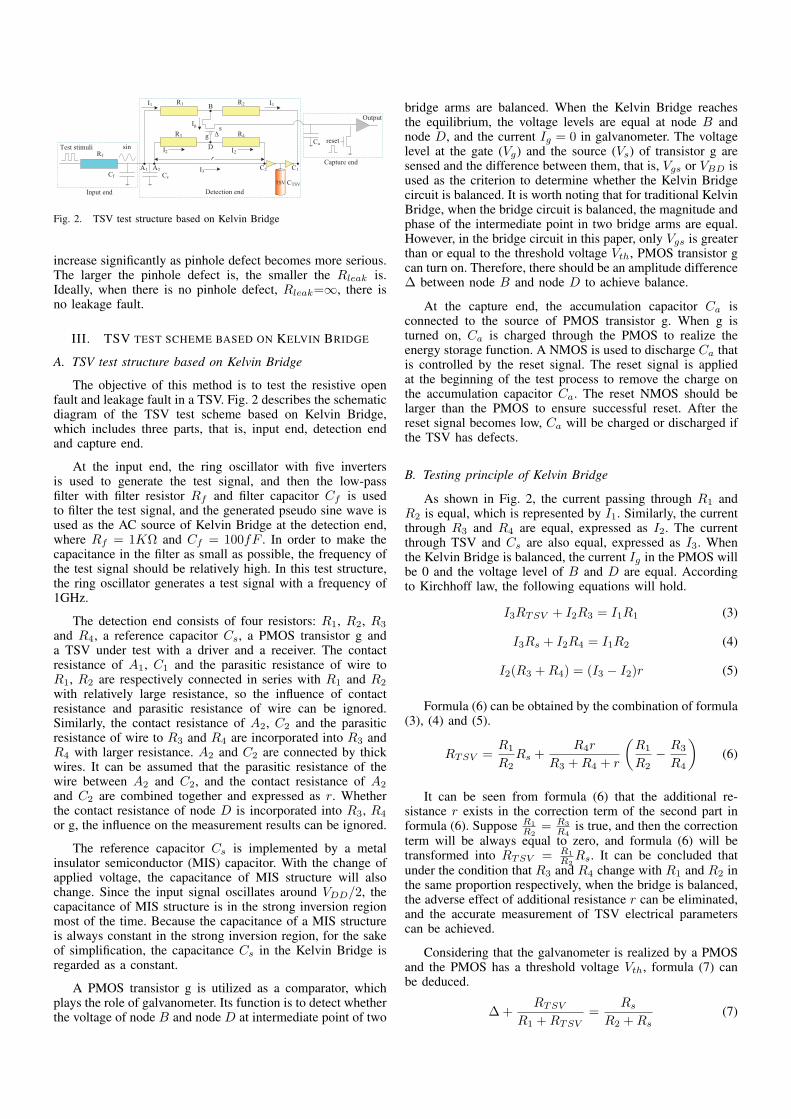
Fig. 2. TSV test structure based on Kelvin Bridge
increase significantly as pinhole defect becomes more serious.The larger the pinhole defect is, the smaller the Rleak is.Ideally, when there is no pinhole defect, Rleak=∞, there isno leakage fault.
III. TSV TEST SCHEME BASED ON KELVIN BRIDGE
A. TSV test structure based on Kelvin Bridge
The objective of this method is to test the resistive openfault and leakage fault in a TSV. Fig. 2 describes the schematicdiagram of the TSV test scheme based on Kelvin Bridge,which includes three parts, that is, input end, detection endand capture end.
At the input end, the ring oscillator with five invertersis used to generate the test signal, and then the low-passfilter with filter resistor Rf and filter capacitor Cf is usedto filter the test signal, and the generated pseudo sine wave isused as the AC source of Kelvin Bridge at the detection end,where Rf = 1KΩ and Cf = 100fF . In order to make thecapacitance in the filter as small as possible, the frequency ofthe test signal should be relatively high. In this test structure,the ring oscillator generates a test signal with a frequency of1GHz.
The detection end consists of four resistors: R1, R2, R3
and R4, a reference capacitor Cs, a PMOS transistor g anda TSV under test with a driver and a receiver. The contactresistance of A1, C1 and the parasitic resistance of wire toR1, R2 are respectively connected in series with R1 and R2
with relatively large resistance, so the influence of contactresistance and parasitic resistance of wire can be ignored.Similarly, the contact resistance of A2, C2 and the parasiticresistance of wire to R3 and R4 are incorporated into R3 andR4 with larger resistance. A2 and C2 are connected by thickwires. It can be assumed that the parasitic resistance of thewire between A2 and C2, and the contact resistance of A2
and C2 are combined together and expressed as r. Whetherthe contact resistance of node D is incorporated into R3, R4
or g, the influence on the measurement results can be ignored.
The reference capacitor Cs is implemented by a metalinsulator semiconductor (MIS) capacitor. With the change ofapplied voltage, the capacitance of MIS structure will alsochange. Since the input signal oscillates around VDD/2, thecapacitance of MIS structure is in the strong inversion regionmost of the time. Because the capacitance of a MIS structureis always constant in the strong inversion region, for the sakeof simplification, the capacitance Cs in the Kelvin Bridge isregarded as a constant.
A PMOS transistor g is utilized as a comparator, whichplays the role of galvanometer. Its function is to detect whetherthe voltage of node B and node D at intermediate point of two
bridge arms are balanced. When the Kelvin Bridge reachesthe equilibrium, the voltage levels are equal at node B andnode D, and the current Ig = 0 in galvanometer. The voltagelevel at the gate (Vg) and the source (Vs) of transistor g aresensed and the difference between them, that is, Vgs or VBD isused as the criterion to determine whether the Kelvin Bridgecircuit is balanced. It is worth noting that for traditional KelvinBridge, when the bridge circuit is balanced, the magnitude andphase of the intermediate point in two bridge arms are equal.However, in the bridge circuit in this paper, only Vgs is greaterthan or equal to the threshold voltage Vth, PMOS transistor gcan turn on. Therefore, there should be an amplitude difference∆ between node B and node D to achieve balance.
At the capture end, the accumulation capacitor Ca isconnected to the source of PMOS transistor g. When g isturned on, Ca is charged through the PMOS to realize theenergy storage function. A NMOS is used to discharge Ca thatis controlled by the reset signal. The reset signal is appliedat the beginning of the test process to remove the charge onthe accumulation capacitor Ca. The reset NMOS should belarger than the PMOS to ensure successful reset. After thereset signal becomes low, Ca will be charged or discharged ifthe TSV has defects.
B. Testing principle of Kelvin Bridge
As shown in Fig. 2, the current passing through R1 andR2 is equal, which is represented by I1. Similarly, the currentthrough R3 and R4 are equal, expressed as I2. The currentthrough TSV and Cs are also equal, expressed as I3. Whenthe Kelvin Bridge is balanced, the current Ig in the PMOS willbe 0 and the voltage level of B and D are equal. Accordingto Kirchhoff law, the following equations will hold.
I3RTSV + I2R3 = I1R1 (3)
I3Rs + I2R4 = I1R2 (4)
I2(R3 +R4) = (I3 − I2)r (5)
Formula (6) can be obtained by the combination of formula(3), (4) and (5).
RTSV =R1
R2Rs +
R4r
R3 +R4 + r
(R1
R2− R3
R4
)(6)
It can be seen from formula (6) that the additional re-sistance r exists in the correction term of the second part informula (6). Suppose R1
R2= R3
R4is true, and then the correction
term will be always equal to zero, and formula (6) will betransformed into RTSV = R1
R2Rs. It can be concluded that
under the condition that R3 and R4 change with R1 and R2 inthe same proportion respectively, when the bridge is balanced,the adverse effect of additional resistance r can be eliminated,and the accurate measurement of TSV electrical parameterscan be achieved.
Considering that the galvanometer is realized by a PMOSand the PMOS has a threshold voltage Vth, formula (7) canbe deduced.
∆+RTSV
R1 +RTSV=
Rs
R2 +Rs(7)

1.3405 1.341 1.3415 1.342 1.34251.34
Time (us)
0.2
0.4
0.6
0.8
Vo
ltag
e (
V) Vg
Vs
Fig. 3. Voltage waveform of the gate Vg and the source Vs on the PMOStransistor g
In addition, in the case of AC power supply, formula (7)is equivalent to the following formula (8).
∆+
1jωCTSV
R1 +1
jωCTSV
=
1jωCs
R2 +1
jωCs
(8)
Here, ∆=Vth/VDD, Cs is the reference capacitance,RTSV and CTSV are the resistance and capacitance of theTSV to be tested respectively.
It can be seen from the equation above that ∆ is a complexnumber, but we only need to consider the real part of ∆, notthe imaginary part, since the phase difference between the twoarms is very small. Due to voltage difference ∆, the resistorand capacitor of the two arms is different from that of thegeneral AC bridges. If the bridge circuit is unbalanced, forexample, the voltage difference is larger than ∆, the PMOSwill be turned on.
Assuming that the TSV capacitance is 60 fF , the voltagewaveforms of the gate Vg and the source Vs on the PMOStransistor g are shown in Fig. 3 to illustrate the operationprocess of the Kelvin Bridge. When Vg is less than Vs andthe voltage difference reaches Vth, the PMOS g will be turnedon and thus Ca is connected to the source node.
At the capture end, the Ca is used as an accumulator and isset to 50 fF . When the voltage passing through Ca is higherthan the threshold value of the connected buffer, the outputwill be flipped from low level to high level.
IV. SIMULATION RESULTS AND ANALYSIS
In order to evaluate the performance, detection range, androbustness against PVT of proposed KB method, HSPICEis used to simulate in 45 nm process. The process modeluses 45 nm PTM CMOS process[18][19], and the referencevoltage VDD is 1.1 V . In the simulation, it is assumed thatresistive open fault occurs in the middle of TSV. The detailedparameters used in the test structure are listed in Table I. Theappropriate method to select the bridge arm resistance will beintroduced later in this section. For the sake of simplification,the parasitic resistance and capacitance of TSV are assumedto be 60 mΩ and 200 fF respectively.
A. Test resolution of resistive open fault
In this section, a PMOS g in Fig. 2 is used as a comparatorto detect whether the intermediate points B and D of the twobridge arms are balanced. The voltage level at the gate (Vg)and source (Vs) of PMOS g are sensed, and the differencebetween them is used as the criterion to determine whether theKelvin Bridge is balanced, so as to characterize the resistive
TABLE I. PARAMETERS USED IN KB TEST STRUCTURE
Symbol Value Tolerance Position
Rf 1KΩ 0, 10% Input endCf 100fF 0, 10% Input endR1 60Ω 0, 10% Detection endR2 60KΩ 0, 10% Detection endR3 20Ω 0, 10% Detection endR4 20KΩ 0, 10% Detection endCs 200fF 0, 10% Detection end
RTSV 60mΩ Detection endCTSV 200fF Detection endCa 50fF 0, 10% Capture end
625
635
645
655
665
Vo
lta
ge a
t in
term
ed
iate
po
int
(m
V)
Rvoid ( )
Voltage at intermediate point V1 (mV)
Voltage at intermediate point V2 (mV)
Fig. 4. Characteristic curve of voltage at intermediate point under resistiveopen fault
open fault and leakage fault in a TSV. Assuming that theinitial state of Kelvin Bridge is in the state of equilibrium,the measured voltage of VBD is 651.263 mV . After injectingresistive open fault or leakage fault into TSV, the slightfluctuation of voltage VBD at equilibrium point can be utilizedto detect the fault. Fig. 4 depicts the characteristic curveof voltage at intermediate point under resistive open fault.In general, the characteristic curve can be divided into leftand right parts, which are drawn in blue and orange, andrepresented by V1 and V2 respectively.
In the right part, when the range of Rvoid is in theinterval [1500Ω, 1MΩ] , the value of V2 gradually increasedfrom 626.886 mV to 659.875 mV , showing an obviousincreasing trend with Rvoid. When the range of Rvoid liesin the range of [1MΩ, 5MΩ], the value of V2 is in theinterval [659.875mV, 659.963mV ]. At this time, the growthrate of V2 is relatively gentle, close to the saturation state,and the intermediate point voltage basically does not continueto increase. Combined with the electrical model of resistiveopen fault, when Rvoid increases to 1MΩ, it can be consideredthat TSV has completely broken at the position h/2.
In the left half, as Rvoid decrease gradually from 1500Ω to 0.1 Ω, the value of increased from 626.886 mV to651.262 mV . In particular, the value of V1 remains constant at651.262 mV when Rvoid is 0.1 Ω, which is very close to theintermediate point voltage in the balanced state. This showsthat as the Rvoid becomes smaller and smaller, the TSV tendsto be in the ideal fault free state. TSV can be treated as faultfree when Rvoid = 0.1Ω, which is the weakest resistive openfault that KB scheme can detect.
The existing BIST schemes are usually easier to detectmedium or severe resistive open faults. However, the resistiveopen faults with lower Rvoid are usually more difficult todetect. Therefore, the minimum value of Rvoid that can bedetected is usually one of the important reference criteria toevaluate a BIST Scheme. As far as we know, it has been

200
300
400
500
600
700
10
0
30
0
50
0
70
0
90
0
11
00
13
00
15
00
17
00
19
00
3k
5k
7k
9k
20
k
40
k
60
k
80
k
10
0k
30
0k
50
0k
70
0k
90
0k
2M
4M
6M
8M
10
M
Vo
lta
ge a
t in
term
ed
iate
pin
t (m
V)
Rleak ( )
Voltage at intermediate point (mV)
Fig. 5. Characteristic curve of voltage at intermediate point under leakagefault
reported in literature that the minimum resistive open fault canbe detected is 200Ω−1KΩ or even higher[8][13][17]. Benefitfrom the excellent detection capability of Kelvin Bridge forsmall and medium resistance, the KB scheme in this paper isobviously superior to most known BIST schemes.
It should be noted that from Fig. 4, it can be found thatone intermediate point voltage corresponds to two Rvoid inthe partial detectable region 0.1Ω − 1MΩ, which will causetest confusion. For example, V1 = V2 = 645mV under thecondition of Rvoid = 200Ω or Rvoid = 6KΩ. In otherwords, when the intermediate point voltage is detected to be645 mV , it is difficult to distinguish the resistive open faultwith 200 Ω or 6 KΩ in a TSV to be tested. This situationcan be explained from the perspective of the electrical modelof the resistive open fault. Under mild resistive open fault,such as less than 1500 Ω, Rvoid has little contribution tothe voltage at intermediate point, but CTSV remains basicallyunchanged and plays a dominant role. However, as Rvoid
increases gradually, especially when Rvoid = 1MΩ, whichindicates that the TSV is completely broken. At this time,CTSV is reduced to half of the original, that is 100 fF , andthe contribution of Rvoid to the voltage at intermediate pointis increased. In practice, the test process needs to be designedreasonably, and it often requires multiple rounds of testingto completely remove the faults in a TSV. Therefore, in theprocess of test practice, the existing BIST method can be usedto conduct a preliminary test to remove the resistive openfault with Rvoid more than 1500 Ω. This step is equivalentto excluding the right half of Fig. 4, and then using the KBscheme in this paper, the fault characteristics of Rvoid from0.1 Ω to 1500 Ω can be detected. Therefore, the KB methodis particularly suitable for the detection of weak open fault.
B. Test resolution of leakage fault
Fig. 5 shows the characteristic curve of the voltage atintermediate point under leakage fault. It can be found thatas the equivalent resistance of leakage fault Rleak increasesfrom 100 Ω to 10 MΩ, the voltage at intermediate pointincreases from 264.954 mV to 651.256 mV . This can beexplained in two aspects. On one hand, under the conditionof Rleak < 100Ω, VBD will be less than 264.954 mV ,galvanometer g fails to conduct, and Ca cannot be chargedor discharged. On the other hand, when Rleak increases from1 MΩ to 10 MΩ, although VBD also increases gradually, ittends to be placid. This shows that when Rleak ≥ 1MΩ, theequivalent resistance of leakage fault is large and the leakagecurrent is very small, which can be considered as approachingthe fault free state. Therefore, in the KB method, the detection
range of leakage fault is [100Ω, 10MΩ], and the preferreddetection range is [100Ω, 1MΩ] as shown in the rectangle inFig. 5.
Through the above analysis, it can be summarized thatthere are three differences between leakage fault and resistiveopen fault. Firstly, leakage fault will not be affected by TSVparasitic capacitance as resistive open fault. Therefore, thecharacteristic curve of leakage fault is a rising curve, whichwill not be divided into two parts as shown in Fig. 4. Secondly,different from the resistive open fault, the smaller the Rvoid
is, the more difficult it is to detect. The larger the equivalentresistance Rleak, the more difficult it is to detect in terms ofleakage fault. Leakage fault with Rleak < 10KΩ is usuallyconsidered to be serious leakage fault, which can be detectedby conventional methods in the preliminary detection. Theequivalent leakage current of Rleak = 10MΩ is 0.1 µA. It canalso be concluded that KB method can detect such a very weakleakage fault as the minimum of 0.1 µA, which is better thanmost existing test methods. At last, compared with the VBD
(651.263 mV ) of fault free, resistive open fault will increasethe VBD, while leakage fault will decrease VBD, which isthe opposite. Assuming that there is only one type of fault,the KB method can successfully distinguish the resistive openfault from the leakage fault according to the voltage VBD atintermediate point.
In a word, the minimum value of resistive open faultdetected by KB method can be achieved by 0.1 Ω, andthe measured resistance Rvoid is very close to the nominalresistance RTSV = 60mΩ of fault free. Furthermore, theKB method can detect a weak leakage fault such as 10MΩ.Therefore, from the view of test accuracy and detectionrange, KB method is a test method with excellent performance.However, each coin has two sides. The KB method cannotdetect serious resistive open fault very well, or KB methodalone will cause some degree of test confusion in terms ofresistive open fault, which is inferior to the existing methods,but can be solved by properly design in the test process. Thisis also make sense as we usually use cursor calipers to achieve0.01 millimeter-level accuracy, however, it is not appropriateto use them to measure objects of meter-level length.
C. The Effect of PVT on the Kelvin Bridge
In order to verify the applicability and robustness ofKB method, the influence of process variation, voltage andtemperature (PVT) of the method is discussed in this section.It is assumed that the fluctuation of resistance and capacitanceused in bridge arm is ±10%. The supply voltage is 0.9 V , 1V and 1.1 V respectively, and the temperature environment is0C, 25C and 105C respectively. Given the supply voltageof 1 V , temperature T= 25 C, comparison of voltage atintermediate point under resistive open fault and leakage faultis depicted in Fig. 6. Here, different values of R and Crepresent different process corners. For example, (0.9R, 1.1C)means that the resistance and capacitance are 0.9 and 1.1times of the standard value respectively. Absolute deviation(AD) is defined as the absolute value of voltage betweenprocess corner and standard corner. Relative deviation (RD)is defined as the average ratio of the voltage at intermediatepoint between the simulation corner and the standard corner.
As shown in Fig. 6, it can be found that both resistive openfault and leakage fault have the minimum RD under process

620
630
640
650
660
0.1 10 300 800 1500 2.3K 4.5K 10K 1M
VBD(mV)
Rvoid ( )
RC
0.9R,0.9C
0.9R,1.1C
1.1R,0.9C
1.1R,1.1C
(a) (b)
500
530
560
590
620
650
500 800 1000 1500 3K 5K 10K 100K 1M
VBD(mV)
Rleak ( )
R,C
0.9R,0.9C
0.9R,1.1C
1.1R,0.9C
1.1R,1.1C
Fig. 6. The voltage distribution at intermediate point under various processcorners. (a) Variation of voltage at intermediate point under resistive openfault. (b) Variation of voltage at intermediate point under leakage fault.
0
5000
10000
15000
20000
50 100 150 200 250 300
Respon
se d
ela
y (
ns)
Capacitance of TSV (fF)
Vdd=0.9 V, 0
Vdd=1.0 V, 0
Vdd=1.1 V, 0
Vdd=0.9 V, 25
Vdd=1.0 V, 25
Vdd=1.1 V, 25
Vdd=0.9 V, 105
Vdd=1.0 V, 105
Vdd=1.1 V, 105
Fig. 7. Response delay of KB test architecture under different PVT corners.
corner (0.9R, 0.9C) and the maximum RD under processcorner (0.9R, 1.1C). It can be concluded that TSV capacitancehas more influence on process variation. In addition, it shouldbe noted that in each process corner, with the increase ofRleak, the AD shows an increasing trend, which is differentfrom Rvoid. In general, the KB test method proposed in thispaper has a good adaptability in all process corners, and isnot sensitive to the variation of resistance and capacitance.
Fig. 7 shows the relationship between the TSV capacitanceand the response delay of KB test circuit at various PVTcorners. It can be seen that the overall distribution of responsedelay presents an obvious three beam curve at 0C, 25Cand 105C. On the contrary, the curves fluctuate little underthe same temperature and different supply voltage. Aftercalculation, the range of output delay fluctuation is ±3%. Inaddition, the longest response delay can be found at (1.1V,0C). It can be concluded that the temperature deviation hasmore influence on the response delay than the supply voltagedeviation.
V. CONCLUSION
Different from the serious fault, the weak fault is usuallymore difficult to be detected, which will leave a hidden dangerto the later process, yield and reliability. Conversely, highertest accuracy can reduce the escape rate of failure, whichis conducive to improve the yield and product quality of3D ICs. The test structure based on Kelvin Bridge proposedin this paper can detect the resistive open fault of 0.1 Ωlevel successfully, which is very close to the ideal fault free.In addition, it can detect 10 MΩ leakage fault, which isequivalent to 0.1 µA leakage current, while PVT analysisproves the effectiveness of the proposed scheme.
VI. ACKNOWLEDGEMENT
This research was supported in part by the National NaturalScience Foundation of China under grant No. (61704001,
618741756, 61904001), the Major National Scientific In-strument and Equipment Development Project under Grant62027815, Anhui Provincial Natural Science Foundation un-der grant No. (1808085QF196, 1908085QF272).
REFERENCES
[1] J. Li, X. Qiang, and B. Eklow, ”On Effective Through-Silicon ViaRepair for 3-D-Stacked ICs,” IEEE Transactions on Computer-AidedDesign of Integrated Circuits and Systems, vol. 32, pp. 559-571, 2013.
[2] B. Noia and K. Chakrabarty, ”Pre-bond probing of TSVs in 3Dstacked ICs,” in IEEE International Test Conference (ITC), Anaheim,California, USA, 2011, pp. 1-10.
[3] N. Kandalaft, R. Rashidzadeh, and M. Ahmadi, ”Testing 3-D ICThrough-Silicon-Vias (TSVs) by Direct Probing,” IEEE Transactionson Computer-Aided Design of Integrated Circuits and Systems, vol.32, pp. 538-546, 2013.
[4] Z. Xiaolong, L. Huiyun, J. Li, et al., ”A Low-Cost TSV Test and Diag-nosis Scheme Based on Binary Search Method,” IEEE Transactions onVery Large Scale Integration (VLSI) Systems, vol. 23, pp. 2639-2647,2015.
[5] G. D. Natale, M. L. Flottes, B. Rouzeyre, et al., ”Built-in self-testfor manufacturing TSV defects before bonding,” in IEEE VLSI TestSymposium (VTS), Napa, California, USA, 2014, pp. 1-6.
[6] C. Wang, J. Zhou, R. Weerasekera, et al., ”BIST methodology, architec-ture and circuits for pre-bond TSV testing in 3D stacking IC systems,”IEEE Transactions on Circuits and Systems I: Regular Papers, vol. 62,pp. 139-148, 2015.
[7] K. Xu, Y. Yu, and X. Peng, ”TSV Fault Modeling and A BIST Solutionfor TSV Pre-bond Test,” in 2021 IEEE 39th VLSI Test Symposium(VTS), 2021, pp. 1-6.
[8] R. Rodriguez-Montaes, D. Arumi, and J. Figueras, ”Postbond Test ofThrough-Silicon Vias With Resistive Open Defects,” IEEE Transactionson Very Large Scale Integration (VLSI) Systems, vol. 27, pp. 2596-2607, 2019.
[9] D. Sergej and C. Krishnendu, ”Contactless pre-bond TSV fault diag-nosis using duty-cycle detectors and ring oscillators,” in 46th IEEEInternational Test Conference, ITC 2015, 2015, pp. 1-10.
[10] L. R. Huang, S. Y. Huang, S. Sunter, et al., ”Oscillation-Based PrebondTSV Test,” IEEE Transactions on Computer-Aided Design of IntegratedCircuits and Systems, vol. 32, pp. 1440-1444, 2013.
[11] S. Pei, A. A. Rabehb, and S. Jin, ”On-Chip Ring Oscillator BasedScheme for TSV Delay Measurement,” in 2017 IEEE 26th Asian TestSymposium (ATS), 2017, pp. 11-16.
[12] C. Hao, X. Yong, and N. Tianming, ”A Test Method for Large-size TSVConsidering Resistive Open Fault and Leakage Fault Coexistence,” in2021 International Symposium on VLSI Design, Automation and Test(VLSI-DAT), Hsinchu, 2021, pp. 1-4.
[13] C. Hao and L. Huaguo, ”Pulse Shrinkage Based Pre-bond ThroughSilicon Vias Test in 3D IC,” in IEEE VLSI Test Symposium (VTS),Napa,California, USA, 2015, pp. 96-101.
[14] T. Ni, H. Chang, T. Song, et al., ”Non-intrusive Online DistributedPulse Shrinking Based Interconnect Testing in 2.5D IC,” IEEE Trans-actions on Circuits and Systems II: Express Briefs, vol. 67, pp. 2657-2661, 2020.
[15] Y. Yu, X. Fang, and X. Peng, ”A Post-bond TSV Test Method basedon RGC Parameters Measurement,” IEEE Transactions on Computer-Aided Design of Integrated Circuits and Systems, vol. 39, pp. 506-519,2020.
[16] Y. Huang, C. Pan, S. Lin, et al., ”Machine-Learning Approach inDetection and Classification for Defects in TSV-Based 3-D IC,” IEEETransactions on Components, Packaging and Manufacturing Technol-ogy, vol. 8, pp. 699-706, 2018.
[17] M. Yi, J. Bian, T. Ni, et al., ”A Pulse Shrinking-Based Test Solutionfor Prebond Through Silicon via in 3-D ICs,” IEEE Transactions onComputer-Aided Design of Integrated Circuits and Systems, vol. 38,pp. 755-766, 2019.
[18] PTM. 45nm Predictive Technology Model. Accessed: July 20th, 2021.[Online] Available: http://ptm.asu.edu.
[19] Nangate. Nangate 45nm Open Cell Library. Accessed: July 20th, 2021.[Online] Available: http://ptm.asu.edu.