Embed Size (px)
Citation preview

FACHBEREICH PHYSIK
Elektronik�Praktikum
Measurement and Control System epst2l.tex KB 20010908
Based upon a single-chip microcontroller a measurement and control systemwas designed which allows a flexible configuration of its functions. It is primarilyintended for applications in students labs, first of all it will be used in the elec-tronics lab [1]. Besides a power supply for the typical voltages needed (+5 V,+12 V, +15 V, -15 V), the unit presently contains 4 A/D-converters (12 Bit, -10. . . +10 V), 4 D/A-converters (12 Bit, 2 voltage outputs -10. . . +10 V, 2 currentoutputs -20. . . +20 mA), 8 digital inputs and 8 digital outputs (TTL), and 8 relayswith one commutating switch each.
The single-chip controller used (Beck IPC@CHIP SC12) is compatible with theformer PC/XT standard (Intel 80186), programs can be built using 16-bit com-pilers for this type of processor (Borland C, Microsoft Visual C++ version 1.52).The controller operating system features a nearly complete DOS with severalextensions including real time operation and controlling of the processor’s I/Opins. Furthermore, a simple TCP/IP functionality is implemented – servers forTelnet, FTP, and WWW. Thus the device allows full remote control via ethernet.

2 Elektronik–Praktikum Physik
Contents
1 Specifications 3
2 Safety Instructions 3
3 The Single-Chip Microcontroller SC12 4
3.1 Functional Overview . . . . . . . . . . . . . . . . . . . . . . . . . . 5
3.2 Pin Configuration . . . . . . . . . . . . . . . . . . . . . . . . . . . . 5
3.3 Address Map (Memory and I/O) . . . . . . . . . . . . . . . . . . . 6
3.4 DOS Extensions . . . . . . . . . . . . . . . . . . . . . . . . . . . . 7
3.5 Configuration . . . . . . . . . . . . . . . . . . . . . . . . . . . . . . 8
4 Hardware of the Measurement and Control System 8
4.1 Block Diagram . . . . . . . . . . . . . . . . . . . . . . . . . . . . . 8
4.2 Address and Data Logic . . . . . . . . . . . . . . . . . . . . . . . . 9
5 Software of the Device 10
5.1 Peripheral Bus . . . . . . . . . . . . . . . . . . . . . . . . . . . . . 10
5.2 I/O Cards on the Peripheral Bus . . . . . . . . . . . . . . . . . . . 13
5.3 Test Programs . . . . . . . . . . . . . . . . . . . . . . . . . . . . . 15
5.4 Socket Implementation . . . . . . . . . . . . . . . . . . . . . . . . . 16
5.5 Ethernet Communications Program . . . . . . . . . . . . . . . . . . 17
6 PC Programs 19
6.1 C/C++ – UNIX (Linux) . . . . . . . . . . . . . . . . . . . . . . . . . 19
6.2 C/C++ – Windows . . . . . . . . . . . . . . . . . . . . . . . . . . . 20
6.3 Microsoft Foundation Classes (MFC) . . . . . . . . . . . . . . . . . 21
6.4 Visual Basic . . . . . . . . . . . . . . . . . . . . . . . . . . . . . . . 22
6.5 Java and MATLAB . . . . . . . . . . . . . . . . . . . . . . . . . . . 23
6.6 Measurement Samples . . . . . . . . . . . . . . . . . . . . . . . . 24
Anhang A: Technische Beschreibung des Herstellers 26
Anhang B: Schaltpläne 30

Measurement and Control System 3
1 Specifications
Measurement and Control Unit:
� Single-chip controller SC12,
� 10baseT Ethernet adapter,
� 2 serial ports ,
� 4 A/D-converter inputs 12 bit, -10. . . +10 V,
� 2 D/A-converter outputs 12 bit, -10. . . +10 V, max. �20 mA,
� 2 D/A-converter outputs 12 bit, -20. . . +20 mA, max. �10 V,
� 8 digital outputs, TTL,
� 8 digital inputs, TTL,
� 8 relays, one commutating switch, maximum current 1 A.
Power Supply for experimental setups, independent of the Measurement andControl Unit, seperate mains switch:
� +5 V, max. 5 A,
� +12 V, max. 1 A,
� +15 V, max. 1 A,
� -15 V, max. 0.5 A.
2 Safety Instructions
For safety reasons all internal and external voltages are ground based. Thus allblack output terminals are connected to ground.
Never plug a device with ground wire to a mains plug without one.
According to the regulations of EMVG valid since 01.01.1996 the device is al-lowed for internal use only.
Repairs, alterations, or expansions are only allowed by skilled personnel.
4 Elektronik–Praktikum Physik
3 The Single-Chip Microcontroller SC12
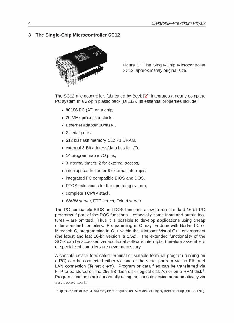
Figure 1: The Single-Chip MicrocontrollerSC12, approximately original size.
The SC12 microcontroller, fabricated by Beck [2], integrates a nearly completePC system in a 32-pin plastic pack (DIL32). Its essential properties include:
� 80186 PC (AT) on a chip,
� 20 MHz processor clock,
� Ethernet adapter 10baseT,
� 2 serial ports,
� 512 kB flash memory, 512 kB DRAM,
� external 8-Bit address/data bus for I/O,
� 14 programmable I/O pins,
� 3 internal timers, 2 for external access,
� interrupt controller for 6 external interrupts,
� integrated PC compatible BIOS and DOS,
� RTOS extensions for the operating system,
� complete TCP/IP stack,
� WWW server, FTP server, Telnet server.
The PC compatible BIOS and DOS functions allow to run standard 16-bit PCprograms if part of the DOS functions – especially some input and output fea-tures – are omitted. Thus it is possible to develop applications using cheapolder standard compilers. Programming in C may be done with Borland C orMicrosoft C, programming in C++ within the Microsoft Visual C++ environment(the latest and last 16-bit version is 1.52). The extended functionality of theSC12 can be accessed via additional software interrupts, therefore assemblersor specialized compilers are never necessary.
A console device (dedicated terminal or suitable terminal program running ona PC) can be connected either via one of the serial ports or via an EthernetLAN connection (Telnet client). Program or data files can be transferred viaFTP to be stored on the 256 kB flash disk (logical disk A:) or on a RAM disk1.Programs can be started manually using the console device or automatically viaautoexec.bat.
1 Up to 256 kB of the DRAM may be configured as RAM disk during system start-up (CHIP.INI).

Measurement and Control System 5
3.1 Functional Overview
The block diagram in Figure 2 shows the hardware concept of the SC12 micro-controller. The central unit is a 80186 CPU clocked at 20 MHz. Total memorysize is 1 MByte, 512 kByte each flash EPROM and DRAM. Half of the flashmemory is occupied by the controller firmware, BIOS and DOS with their specificextensions, the other half is configured as logical disk (volume A:). Furthermore,the system contains a watchdog circuit and various I/O blocks (Ethernet, 2 serialports, DMA, programmable I/O lines, timer, interrupt inputs, I2C bus).
Figure 2: Functional blocks integrated in the SC12 (schematic overview).
The complete address range of the 80186 is only internally accessible (20 bitmemory, 16 bit I/O addressing). Peripherals can be connected to the externalmultiplexed 8-bit address/data bus. Some other external pins may be used asadditional address lines or as chip-select lines when configured appropriately toselect 8-bit blocks in the I/O address range (the chip-select lines correspond tothe decoded address bits 8, 9, and 10).
3.2 Pin Configuration
As can be derived from the block diagram in Figure 2, 32 connection pins arenot sufficient to separate all pin functions. Many of the pins thus have to bemultifunctional (Figure 3). An application, which wants to use a certain pin func-tionality, first has to program the pins to the functions desired.

6 Elektronik–Praktikum Physik
Figure 3: Pin Configuration of the SC12.
Figure 4: Memory and I/O map of the SC12 microcontroller. The 8-bitblocks in the I/O region can be addressed using the chip select lines shown(PCS0. . .PCS6).
3.3 Address Map (Memory and I/O)
The CPU 80186 has an address space of 1 MByte for memory and 64 kBytefor I/O (20 bit and 16 bit, resp.). Within the SC12 the memory address space iscompletely filled by the memory integrated as shown in Figure 4: 512 kByte flashEPROM and 512 kByte DRAM. As usual in PCs, the lower part of the addressrange is occupied by RAM, the upper by ROM. Half of the flash memory is

Measurement and Control System 7
configured as writable, non volatile disk (volume A:), at most half of the RAMcan be used as a RAM disk (volume E:). In the I/O range not all addresses areaccessible. Instead the SC12 features a combination of chip select lines andthe 8 lower address bits (if more address lines would be needed, the PIO pinscould be programmed for this purpose). With the chip select lines separate 8-bitblocks are selected (one out of six) when the respective range is addressed.Thus PCS0 is active (low) when using an I/O address in the range 0 – 0xFF,PCS1 for addresses between 0x100 and 0x1FF, and so on.
3.4 DOS Extensions
To control the extended functionality of the SC12 microcontroller, several addi-tional software interrupts have been included into the usual framework of DOSsystem calls. Every logical group of functions is attached to one of the soft-ware interrupts in the range 0xA0. . . 0xAF, the individual function in the group isselected through register AH. Parameters are passed via other CPU registers.
The additional software interrupts include:
0xA1, HAL_INT: Hardware Abstraction Layer, hardware control (data bus, programmableinput/output lines, timer).
0xA2, PFE_INT: Pin Function Enabler, selects the desired functions of the multifunctionalconnection pins.
0xAA, I2C_INT: Functions of the I2C interface.
0xAB, CGI_INT: Configuration of the web server and installation of CGI programs.
0xAC, TCP_INT: Access to the TCP/IP system. Most of the Berkeley-Style funktions areimplemented: open, close, bind, connect, listen, accept,send, receive, ...
0xAD, RTX_INT: Real time extensions to the operating system (RTOS – Real Time Operat-ing System).
A comprehensive description of all software interrupts can be found in the BIOSAPI part of the documentation [3].
In C/C++ software interrupts are called using the function int86x. The follow-ing fragment would make the chip select lines CS0, CS5 and CS6 available forthe application:
const unsigned short PFE_INT = 0xA2;const unsigned char ENABLECS = 0x83;const unsigned short CSMASK = (1<<0) | (1<<5) | (1<<6);...union REGS inregs, outregs;struct SREGS segregs;...inregs.h.ah = ENABLECS;inregs.x.dx = CSMASK;int86x(PFE_INT, &inregs, &outregs, &segregs); .

8 Elektronik–Praktikum Physik
3.5 Configuration
Hardware and TCP/IP system of the SC12 are configured in several steps. Dur-ing system start-up the programmable processor pins are reset to their defaultfunctionality. Then the file CHIP.INI is read and the settings found there areadopted, e. g. IP address, RAM disk, modes of the serial ports, modes, usersand passwords for the TCP/IP services. After that the commands and programsfound in AUTOEXEC.BAT are executed.
Additional configuration steps can be made by every user program through re-spective system calls.
The configuration options are given in great detail and rather completely in thedocumentation [3] provided by the manufacturer. The default configuration ofthe processor pins is described in the IPCChip Initialization section of the BIOSAPI PDF documentation, the valid entries for CHIP.INI in the CHIP.INI Docu-mentation section, the commands for the command interpreter in the CommandProcessor section.
4 Hardware of the Measurement and Control System
In favor of a robust concept not all possibilities provided by the microcontrollerhardware are utilized. Not used is e. g. the multiplexing of addresses and data,as that could cause problems with slow peripheral circuits. Instead a peripheralbus with separate address and data lines is used which even may be run in afully static way.
4.1 Block Diagram
The modular concept of the Measurement and Control System is sketched inFigure 5. Essential part is the SC12 microcontroller with Ethernet connectionand 2 serial ports. Via a suitable logic and driver circuits the peripheral bus withseparate address, data, and control lines is driven. The I/O cards for digital I/O,relays, D/A and A/D converters are connected to this peripheral bus.
Digital I/O Relay DAC ADC
SC12
Logic Address
Data
1 . . . 8Switch
1U
41...8In
1...8Out
2 3I
3 41 2RS232
Ethernet
RS232
Figure 5: Block Diagram of the Measurement and Control System.
Data and address bus are 8 bit wide each. Data thus can be sent as bytes be-tween controller and peripherals. The 4 low order bits of the address bus are

Measurement and Control System 9
used for addressing the I/O cards (base address), the 4 high order bits for addi-tional tasks as e. g. addressing of ADC or DAC channels. The base addresses0 and 0x0F are reserved: 0 should be never used, may be treated as ‘invalidaddress’, 0x0F is used for special purposes like Reset or Calibration.
4.2 Address and Data Logic
SC12
Data
Data
Address
Address
Data OutID In Data In
IOWR
IORD
CS0
IDRD
DATARD
ADWR
DATAWR
CS6
CS5
ControlLogic
CS CS CS CS
Figure 6: Address and data logic of the Measurement and Control System. Thebus driver directions are indicated by arrows. The address lines are latched tohold the respective state statically.
The address and data lines of the peripheral bus are connected to the 8-bit databus of the microcontroller via bus drivers. The principle is shown in Figure 6.Functions implemented include:
� Write address lines (Address),
� Read identification byte (ID In) to verify the type of a certain I/O card2,
� Write data lines (Data Out),
� Read data lines (Data In).
The respective chip select signals for the bus drivers (ADWR, IDRD, DATAWR,DATARD) are formed in the control logic using the appropriate control signal ofthe microcontroller:
ADWR = CS0 & IOWRIDRD = CS0 & IORDDATAWR = CS6 & IOWRDATARD = CS5 & IORD
These signals (right side) have to be provided by the application programs in asuitable way.
Actually the above signals are in negative logic, the equations thus should read:
ADWR = CS0 | IOWR. . . = . . .
Yet to understand the principle as well as to help for programming tasks a de-scription in positive logic is sufficient.
2 Via additional data lines which may be used for other purposes, too.

10 Elektronik–Praktikum Physik
Addresses und ID bytes of the presently available I/O cards are listed in table 1.
Table 1: Base ad-dresses and identifica-tion bytes of the presentI/O cards.
I/O Card Address ID Byte
Digital-I/O 4 0x0D
Relays 6 0x0B
Analog-to-Digital-Converter 8 0x0C
Digital-to-Analog-Converter 9 0x0E
5 Software of the Device
Software for the device can be written on a PC using 16-bit compiler for MS-DOS, if necessary also using assembler code directly. The program fragmentsdescribed here were built within the Microsoft Visual-C++ development environ-ment. The version to be used is 1.52 (from 1993) or an earlier one, later versionsbuild 32-bit code only.
Several of the project options have to be changed from the presets: for ‘ProjectType’ MS-DOS application (.EXE) has to be chosen, for ‘CPU’ 80186 / 80188,and for ‘Structure Member Byte Alignment’ 1 Byte. It is advisable to build the pro-grams always in ‘Release Mode’, as they usually can not be run (and debugged)on the host computer. The programs are transferred to the microcontroller via anFTP connection, they may be started from a console device (terminal programon a PC) using a Telnet connection or one of the serial ports3. As FTP programin Windows e. g. WS_FTP from Ipswitch [4] may be used. A convenient terminalprogram for Telnet or serial port connections is Tera Term Pro [5]; both arefreely available.
5.1 Peripheral Bus
The definitions and C++ classes for the peripheral bus are collected in theheader file IOPORT.H.
First of all meaningful symbols for the parameters of the hard- and software aredefined:
typedef unsigned short USHORT;
const USHORT CSAD = 0, // Chip SelectsCSID = 0,CSRD = 5,CSWR = 6;
const USHORT PFE_INT = 0xA2, // Pin Function ConfigurationENABLEDATA = 0x80,ENABLECS = 0x83,NOALE = 0,BIDIRECT = 0xFFFF,
3 The baud rate of the serial ports can be changed in the file CHIP.INI (described in the CHIP.INIDocumentation section of the BIOS API documentation [ 3]), preset is 19200 baud. Fixed setare 8 data bits, no parity and one stop bit.

Measurement and Control System 11
CSMASK = (1<<CSAD) | (1<<CSID)| (1<<CSRD) | (1<<CSWR);
const USHORT ADDIO = 4, // Standard AddressesADREL = 6,ADADC = 8,ADDAC = 9,ADCAL = 15; // Calibration
const USHORT IDREL = 0x0b, // Identification BytesIDDIO = 0x0d,IDADC = 0x0c,IDDAC = 0x0e;
struct portID {USHORT id;char * idstring;
};const struct portID ID[] = {{IDREL, "Relay"},{IDDIO, "Digital I/O"},{IDADC, "ADC"},{IDDAC, "DAC"}
};
The first two groups denote specifics of the hardware concept – chip select linesand constants for the pin configurations of the microcontroller. The remainingconstants include the presently available I/O cards – standard addresses, iden-tification bytes, identification strings.
The class IOConfig implements the DOS calls for the pin configuration – ALEis deactivated, the data bus is set to bidirectional operation, the necessary chipselect lines are activated:
class IOConfig {private:void EnableData() {
union REGS inregs, outregs;struct SREGS segregs;inregs.h.ah = ENABLEDATA;inregs.h.al = NOALE;inregs.x.dx = BIDIRECT;int86x(PFE_INT, &inregs, &outregs, &segregs);
}void EnableCS() {
union REGS inregs, outregs;struct SREGS segregs;inregs.h.ah = ENABLECS;inregs.x.dx = CSMASK;int86x(PFE_INT, &inregs, &outregs, &segregs);
}public:IOConfig() {
EnableData();EnableCS();

12 Elektronik–Praktikum Physik
}};
The constructor of the class runs the two functions necessary to configure thepin functionality.
The class IOPort then implements the software statements needed for thetreatment of the peripheral bus as described in section 4.2 – AddressWr,IdRd, DataWr, DataRd select and write or read the respective latches. Theparticular chip select lines of the microcontroller are activated by the appropri-ate I/O addresses (CS<<8). The combination of address and data yields thecombined I/O commands OutPort and InPort, we are accustomed to:
class IOPort : private IOConfig {protected:USHORT addr;enum {HBE = 1<<4};
void AddressWr(USHORT address) {_outp(CSAD<<8, address);
}USHORT IdRd() {
return _inp(CSID<<8);}void DataWr(USHORT data) {
_outp(CSWR<<8, data);}USHORT DataRd() {
return _inp(CSRD<<8);}void OutPort(USHORT address, USHORT data) {
AddressWr(address);DataWr(data);
}USHORT InPort(USHORT address) {
AddressWr(address);return DataRd();
}public:IOPort(USHORT a) : addr(a) {}USHORT Addr() { return addr; }USHORT Identify() {
AddressWr(addr);return IdRd();
}char * IDString() {
USHORT thisID = Identify();for (int i=0; i<sizeof(ID)/sizeof(portID); i++)if (ID[i].id == thisID)
return ID[i].idstring;return "";
}};
The class is based on (inherits) IOConfig, in the class constructor thus also

Measurement and Control System 13
the constructor of the base class is called. That means that automatically theright pin configuration is established when an application uses an IOPort ob-ject. Identify and IDString can be used to identify the I/O cards.
5.2 I/O Cards on the Peripheral Bus
Based on IOPort are the classes for the I/O cards of the system (also in thefile IOPORT.H). The addresses are set to their default values if not changed bythe calling program.
The constructors of the derived classes first check whether the right card ispresent at the address given, otherwise the address (addr) is set to zero (invalidaddress). An application that wants to use a specific I/O card can check theaddress using the function Addr of the base class IOPort which is inheritedby all derived classes. If this address is zero, the application may act accordingly.On the other hand an I/O command using address zero will have no effect asthere should be never a peripheral using this address.
The class DigitalIO contains the functions Write and Read to set andread the TTL inputs and outputs of the digital I/O card:
class DigitalIO : public IOPort {public:DigitalIO(USHORT addr = ADDIO) : IOPort(addr) {
if (Identify()!=IDDIO)addr = 0;
}void Write(USHORT data) {
OutPort(addr, data);}USHORT Read() {
return InPort(addr);}
};
For the relay card only the Write–function is defined (the ‘real existing’ hard-ware necessitates the complement of the data):
class Relay : public IOPort {public:Relay(USHORT addr = ADREL) : IOPort(addr) {
if (Identify()!=IDREL)addr = 0;
}void Write(USHORT data) {
OutPort(addr, ~data); }};
The Write–function in the class DAC for the digital-to-analog-converters is alittle bit more complex because of the four output channels of the card. Accordingto the front panel labelling of the system a channel address 1. . . 4 is used whichis translated to the internal counting 0. . . 3 and shifted to the address bits 5 and6. Address bit 4 enables the high order 4 bits of the 12-bit output value (HBE),address bit 7 (LE) – when low – latches the complete stored value to the output.

14 Elektronik–Praktikum Physik
A further minor complication is caused by the output amplifiers. For the twovoltage outputs (channels 1 and 2) a digital value of 0 corresponds to a voltageof 10 V, a value of 4095 to a voltage of -10 V, for the current outputs (channels3 and 4) digital 0 corresponds to -20 mA, digital 4095 to +20 mA. The softwareprovides for a proper translation such that a digital value of 2047 corresponds tothe maximal positive, a value of -2047 to the maximal negative output value foreach channel.
class DAC : public IOPort {private:enum {LE = 1<<7};
public:DAC(USHORT addr = ADDAC) : IOPort(addr) {
if (Identify()!=IDDAC)addr = 0;
}void Write(USHORT channel, short data) {
channel--;if (channel>3)return;
if (channel<2)data = 2048-data;
elsedata = 2048+data;
USHORT ad = addr | (channel<<5) | LE;OutPort(ad, data);ad = addr | (channel<<5) | HBE;OutPort(ad, data>>8);AddressWr(0);
}};
In the Read–function of the class ADC for the analog-to-digital-converter inputsthe channel address is formed in a similar way as in DAC and shifted to theaddress bits 6 and 7. The A/D conversion is initiated by an output commandto the respective address, after a short delay the converted value is available.Again HBE has to be set to read the 4 high order bits of the 12-bit digital value:
class ADC : public IOPort {private:int n;void Wait(int duration) {
for (int i=0; i<duration; i++)n = i+i;
}public:ADC(USHORT addr = ADADC) : IOPort(addr) {
if (Identify()!=IDADC)addr = 0;
}short Read(USHORT channel) {
channel--;if (channel>3)return 0;

Measurement and Control System 15
USHORT ad = addr | (channel<<6);OutPort(ad, 0);Wait(10);short lobyte = DataRd() & 0xFF;short hibyte = InPort(ad | HBE) & 0x0F;AddressWr(0);return (hibyte<<8) + lobyte -2048;
}void Calibrate() {
AddressWr(ADCAL);AddressWr(0);Wait(100);
}};
The input circuit for the 12-bit analog-to-digital converter is configured such thata voltage range of -10. . . +10 V is converted to the digital values 0. . . 4095. Sub-tracting 2048 from this digital value yields a symmetric range -2047. . . +2047 forthe output value which corresponds better to the input range -10. . . +10 V. In thefunction Calibrate of the class the special address for calibration is put tothe address bus and thus a calibration of the A/D converter is initiated.
5.3 Test Programs
Based on the defined classes, simple test programs can be written. The programIdentify lists the I/O cards present in the system:
int main() {printf("\nADDR ID TYPE\n");printf("---------------------\n");for (unsigned short a=1; a<15; a++) {
IOPort p(a);printf("%02X : %02X : %s\n",a, p.Identify(), p.IDString());
}return 0;
}
DAC sets a D/A channel to a certain value:
int main(int argc, char* argv[]){if (argc < 3) {
printf ("\nusage: DAC <channel> <data>\n\n");return 1;
}DAC da;unsigned short channel = atoi(argv[1]);short data = atoi(argv[2]);da.Write(channel, data);return 0;
}
ADC reads and lists all A/D inputs:

16 Elektronik–Praktikum Physik
int main(){ADC ad;printf("\nCHANNEL DATA\n");printf("--------------\n");for (unsigned short chan=1; chan<5; chan++)
printf("%4d %5d\n", chan, ad.Read(chan));return 0;
}
In a similar way the programs Calibr, DigiIO and Relay are working.
5.4 Socket Implementation
The socket functionality necessary for TCP/IP connections is formulated in theclass cSocket in the file SOCKET.H. The function names are mainly chosenaccording to the Berkeley Sockets conventions:
typedef unsigned short USHORT;
static const USHORT TCP_INT = 0xAC;
class cSocket {private:REGS inregs, outregs;SREGS segregs;sockaddr_in Ad, *pAd;recv_params Rdata, *pRd;send_params Sdata, *pSd;short sd;short established;USHORT error;
public:cSocket()
: established(0), error(0), sd(0), pAd(&Ad),pRd(&Rdata), pSd(&Sdata)
{Rdata.flags = MSG_TIMEOUT;Rdata.timeout = 20000L;Sdata.flags = MSG_DONTWAIT;
};~cSocket()
{ };short Create(unsigned char type = SOCK_STREAM);short Connect();short Bind(USHORT port);USHORT HtoNs(USHORT port);short Listen(short n = 1);short Accept(cSocket& T);short DataAvailable();void ReceiveFlags(USHORT Flag, unsigned long Time);short Receive(char * buffer, USHORT n);void SendFlags(USHORT Flag)
{ Sdata.flags = Flag; };short Send(char * buffer, USHORT n);

Measurement and Control System 17
short Send(char * buffer);short Close();short Established()
{ return established; };short GetError()
{ return error; };};
The individual functions are written as C++ wrappers for the unhandy and crypticDOS calls (int86), as example the function Send:
short cSocket::Send(char * buffer, USHORT n){Sdata.bufferPtr = (char *) buffer;Sdata.bufferLength = n;Sdata.toPtr = NULL;Sdata.tolengthPtr = NULL;
inregs.h.ah = API_SEND;inregs.x.bx = sd;inregs.x.dx = FP_SEG(pSd);inregs.x.si = FP_OFF(pSd);int86(TCP_INT, &inregs, &outregs);
if(outregs.x.dx == (USHORT)API_ERROR) {error = outregs.x.ax;return API_ERROR;
}error = 0;return outregs.x.ax;
}
5.5 Ethernet Communications Program
A simple operation program for the Measurement and Control System (SOCK-TEST) corresponds with client programs via Ethernet and responds to their ques-tions. For the connection a server socket is established waiting for connectionrequests:
#ifdef TESTvoid INFO(char * s) { printf(s); }void INFO(char * s, char * t) { printf(s, t); }
#elsevoid INFO(char * s) {}void INFO(char * s, char * t) {}
#endif
const unsigned short BUFSIZE = 1024;const unsigned short TCPPORT = 1234;
int main(){cSocket S, *T;char buffer[BUFSIZE+1];

18 Elektronik–Praktikum Physik
S.Create();S.Bind(TCPPORT);
while(1) { INFO("** Listen\n");S.Listen();T = new cSocket();S.Accept(*T); INFO("** Connect\n");while(T->Established() == 1) {T->Receive(buffer, BUFSIZE); INFO("-> %s\n",buffer);Interprete(buffer); INFO("<- %s",buffer);T->Send(buffer);
}delete T; INFO("** Disconn\n");
}return 0;
}
In the main program main the instruction sequence typical for server sockets:
� Establish the main socket S using Create and Bind,
� Wait for a connection request with Listen,
� Accept the connection using Accept on the previously established helpersocket T,
� T communicates with the client via Receive and Send, until the con-nection is closed by the client.
During the program test (#ifdef TEST), the INFO calls on the right sideprovide for a protocol of the program actions (console output using printf).
Interprete interprets and handles the requests accepted. For the I/O cardsglobal static objects are defined. The possible commands are listed in a constantdefinition:
DigitalIO dio;Relay rel;DAC dac;ADC adc;
const char CMDDIN[] = "di";const char CMDDUT[] = "do <data>"; // <data> = 0..255const char CMDREL[] = "re <data>"; // <data> = 0..255const char CMDDAC[] = "da<n> <data>"; // <n> = 1..4
// <data> = -2047..2047const char CMDADC[] = "ad<n>"; // <n> = 1..4
void Interprete(char * buffer){if (buffer[0]==’\0’)
return;for (char * s = buffer; *s; s++)
tolower(*s);if (strncmp(buffer, CMDDIN, 2)==0)
sprintf(buffer, "%3d\r\n", dio.Read());
Measurement and Control System 19
else if (strncmp(buffer, CMDDUT, 2)==0) {dio.Write(atoi(buffer+3));sprintf(buffer, "OK\r\n");}
else if (strncmp(buffer, CMDREL, 2)==0) {rel.Write(atoi(buffer+3));sprintf(buffer, "OK\r\n");}
else if (strncmp(buffer, CMDDAC, 2)==0) {dac.Write(atoi(buffer+2), atoi(buffer+4));sprintf(buffer, "OK\r\n");}
else if (strncmp(buffer, CMDADC, 2)==0)sprintf(buffer, "%5d\r\n", adc.Read(atoi(buffer+2)));
elsesprintf(buffer, "COMMAND ERROR\r\n");
}
The program responds with ‘OK’ to output instructions, with the measured valueto input instructions or with an error message to instructions not recognized.The answer strings are terminated by an end-of-line sequence (CR, LF), thissimplifies the treatment on the client side (the answer can be read by the Javafunction readLine).
6 PC Programs
PC programs, which want to communicate with the Measurement and ControlSystem, must implement a client socket for this purpose. This client socket hasto establish a connection with the specific TCP/IP port (1234 in the above exam-ple) of the server socket. The following examples illustrate the typical proceedingfor different programming languages.
6.1 C/C++ – UNIX (Linux)
A simple console program establishes an Ethernet connection with the Measure-ment and Control System, sends the keyboard inputs to the device and displaysthe response strings:
#include <stdio.h>#include <string.h>#include <sys/types.h>#include <sys/socket.h>#include <netinet/in.h>#include <netdb.h>
const unsigned short PORT = 1234;const char HOSTNAME[] = "ipc1.physik.uni-osnabrueck.de";
int main(){
int S;const int BUFSIZE = 1024;char inbuf[BUFSIZE], outbuf[BUFSIZE];

20 Elektronik–Praktikum Physik
int n;struct sockaddr_in ad;struct hostent *he;
ad.sin_family = PF_INET;ad.sin_port = htons(PORT);he = gethostbyname(HOSTNAME);memcpy(&ad.sin_addr, he->h_addr, 4);
S = socket(PF_INET, SOCK_STREAM, 0);connect(S, &ad, sizeof(ad));
for (;;) {fgets(inbuf, BUFSIZE, stdin);if ((inbuf[0]==’e’)||(inbuf[0]==’E’))
break;send(S, inbuf, strlen(inbuf), 0);n = recv(S, outbuf, BUFSIZE, 0);outbuf[n] = ’\0’;printf(outbuf);
}
return close(S);}
The first task is to fill the sockaddr_in structure ad which contains theessential information for the connection (IP address and port of the server). Thena client socket is established and connected to the server. The communicationis done by the functions send and recv, close shuts down the connectionat the end of the program.
For clarity no error checks are included in the sample, at least such checksshould be performed after the call to the functions gethostbyname (returns azero pointer to indicate an error) and connect (returns non-zero on error).
6.2 C/C++ – Windows
In Windows (using Microsoft Visual C++ or MinGW), some parts are simpler,some more complex. Thus the list of include files gets shorter:
#include <stdio.h>#include <windows.h>
Socket functionality – in Linux always directly available – has to be initiated inWindows before usage:
WORD wVersionRequested = MAKEWORD( 1, 0 );WSADATA wsaData;WSAStartup( wVersionRequested, &wsaData );
Two of the necessary functions, connect and close, are slightly differentcompared to Linux:
connect(S, (sockaddr *) &ad, sizeof(ad));
Measurement and Control System 21
return closesocket(S);
In the case of an error the error number can be found using the function WSAGet-LastError (all error numbers together with their symbolic names are listed inthe header file winsock.h).
6.3 Microsoft Foundation Classes (MFC)
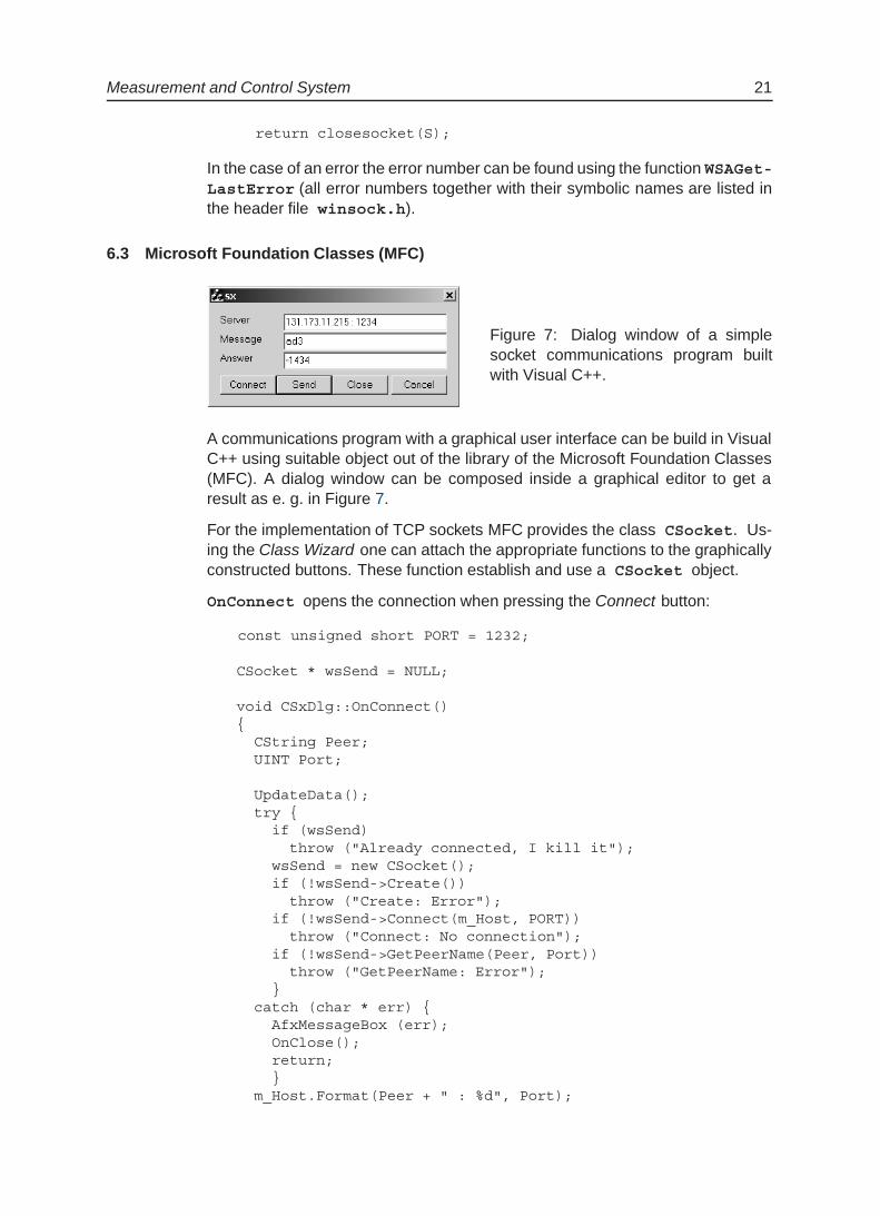
Figure 7: Dialog window of a simplesocket communications program builtwith Visual C++.
A communications program with a graphical user interface can be build in VisualC++ using suitable object out of the library of the Microsoft Foundation Classes(MFC). A dialog window can be composed inside a graphical editor to get aresult as e. g. in Figure 7.
For the implementation of TCP sockets MFC provides the class CSocket. Us-ing the Class Wizard one can attach the appropriate functions to the graphicallyconstructed buttons. These function establish and use a CSocket object.
OnConnect opens the connection when pressing the Connect button:
const unsigned short PORT = 1232;
CSocket * wsSend = NULL;
void CSxDlg::OnConnect(){CString Peer;UINT Port;
UpdateData();try {
if (wsSend)throw ("Already connected, I kill it");
wsSend = new CSocket();if (!wsSend->Create())throw ("Create: Error");
if (!wsSend->Connect(m_Host, PORT))throw ("Connect: No connection");
if (!wsSend->GetPeerName(Peer, Port))throw ("GetPeerName: Error");
}catch (char * err) {
AfxMessageBox (err);OnClose();return;}
m_Host.Format(Peer + " : %d", Port);

22 Elektronik–Praktikum Physik
UpdateData(false);}
The connection is established to the server entered in the field Server (the vari-able for this field is m_Host ). The port used is a fixed constant in the program.After a successful connection GetPeerName requests additional server infor-mation (Peer, Port) which are displayed in the Server field.
OnSend sends the text in field Message (variable m_Send ) to the server, waitsfor a response and displays the response in field Answer (variable m_Recv ):
void CSxDlg::OnSend(){UpdateData();try {
if (!wsSend)throw ("No Socket");
if (wsSend->Send(m_Send, m_Send.GetLength())==SOCKET_ERROR)throw ("Send: Error");
Sleep(100);int n = wsSend->Receive(m_Recv.GetBuffer(1000),1000);m_Recv.ReleaseBuffer(n);}
catch (char * err) { AfxMessageBox (err); }UpdateData(false);
}
The connection is closed by OnClose:
void CSxDlg::OnClose(){delete wsSend;wsSend = NULL;
}
In all functions a C++ type error handling is integrated using try, throw andcatch.
6.4 Visual Basic
To build an application in Visual Basic is even simpler, a dialog window (Figure 8is constructed graphically, too. Not visible there, an object of type Winsock (herusing the name Socket) is inserted. The properties of the object (server nameand port number) are entered here as fixed values using the property menu.
Figure 8: Simpler version using VisualBasic.
The program then only consists of some lines to be added to the frames providedby the programming environment:
Private Sub SendButton_Click()Socket.SendData (TextIn.Text)

Measurement and Control System 23
TextIn.Text = ""TextOut.Text = "Wait"
End Sub
Private Sub Form_Load()Socket.Connect
End Sub
Private Sub Form_Unload(Cancel As Integer)Socket.Close
End Sub
Private Sub Socket_DataArrival(ByVal bytesTotal As Long)Dim Data As StringSocket.GetData (Data)TextOut.Text = Data
End Sub
6.5 Java and MATLAB
The newer versions of MATLAB (starting from release 11) can access the JavaVirtual Machine of the operation system. Using this Java functionality, a MATLABscript (or even a command line sequence) may establish a TCP/IP connectiondirectly without the need to use a helper program (e. g. a MEX file written inC++).
As example a short data acquisition program which controls the D/A output #3(sequence of current values) and inputs values from A/D input #1 (measuredvoltages):
function [v, c] = sockxmplimport java.net.*so = java.net.Socket(’ipc1’, 1234);pause(1);n = 1;for curr=-2000:20:2000,
c(n) = curr;s = sprintf(’da3 %d’, curr);SocketIO(so, s);sData = SocketIO(so, ’ad1’);v(n) = str2double(sData);n = n + 1;
end;pause(1);so.close;
The TCP/IP connection to the Measurement System is opened using java.net.Socketand closed after all using close.
For the handling of the communication a local function SocketIO is definedwhich transforms the MATLAB string to be sent into a Java string before sendingit via the OutputStream object of the socket. From the InputStream objecta BufferedReader is derived, its member function readLine is used toinput the response text of the Measurement System.
24 Elektronik–Praktikum Physik
function recvStr = SocketIO(socket, sendStr)str = java.lang.String(sendStr);out = socket.getOutputStream;out.write(str.getBytes);in = socket.getInputStream;isr = java.io.InputStreamReader(in);ibr = java.io.BufferedReader(isr);recvStr = ibr.readLine;
6.6 Measurement Samples
Using the above MATLAB script, the example measurements of Figures 9 and10 were carried out.
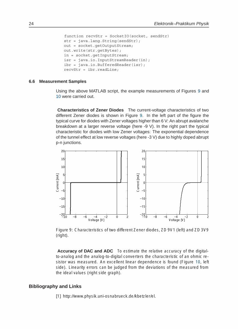
Characteristics of Zener Diodes The current-voltage characteristics of twodifferent Zener diodes is shown in Figure 9. In the left part of the figure thetypical curve for diodes with Zener voltages higher than 6 V: An abrupt avalanchebreakdown at a larger reverse voltage (here -9 V). In the right part the typicalcharacteristic for diodes with low Zener voltages: The exponential dependenceof the tunnel effect at low reverse voltages (here -3 V) due to highly doped abruptp-n junctions.
−10 −8 −6 −4 −2 0 2−20
−15
−10
−5
0
5
10
15
20
Voltage [V]
Cur
rent
[mA
]
−10 −8 −6 −4 −2 0 2−20
−15
−10
−5
0
5
10
15
20
Voltage [V]
Cur
rent
[mA
]
Figure 9: Characteristics of two different Zener diodes, ZD 9V1 (left) and ZD 3V9(right).
Accuracy of DAC and ADC To estimate the relative accuracy of the digital-to-analog and the analog-to-digital converters the characteristic of an ohmic re-sistor was measured. An excellent linear dependence is found (Figure 10, leftside). Linearity errors can be judged from the deviations of the measured fromthe ideal values (right side graph).
Bibliography and Links
[1] http://www.physik.uni-osnabrueck.de/kbetzler/el.

Measurement and Control System 25
−10 −5 0 5 10−20
−15
−10
−5
0
5
10
15
20
Voltage [V]
Cur
rent
[mA
]
−2000 −1000 0 1000 2000−2
−1.5
−1
−0.5
0
0.5
1
1.5
2
Current [D/A−Value]
Dev
iatio
n [B
it]
Figure 10: Linear characteristic of an ohmic resistor, the right graph shows thedeviations of the measured digital values from an ideal linear dependence.
[2] http://www.beck-ipc.de.
[3] http://www.bcl-online.de/mdocumentation/docu.asphttp://www.bcl-online.de/download/api/APIDOC0101B.PDF.
[4] http://www.ipswitch.com/products/index.html.
[5] http://www.vector.co.jp/authors/VA002416/teraterm.html.

26 Elektronik–Praktikum Physik
Anhang A: Technische Beschreibung des Herstellers
Das Steuergerät besteht aus einem 19” Grundgerät mit zwei separat schalt-baren Stromversorgungen, wobei die Ausgangsspannungen und der Netzschal-ter der 2. Stromversorgung an der Frontplatte zugänglich sind. Ein eingebauterSC12 Microprozessor ermöglicht die Kommunikation der Modulsteckplätze übereine serielle Schnittstelle an der Frontplatte oder direkt über eine TCP/IP-Netzverbindung(Western-Steckverbindung an der Rückwand). Alle Steckmodule arbeiten aneinem gemeinsamen 64-poligen Steuer- und Versorgungsbus, der auch an derRückwand zugänglich ist. Es können hier Erweiterungseinheiten oder ein ‘Buss-pion’ angeschlosssen werden. Um Timingproblemen auf den Busleitungen beider Ansteuerung von Modulen aus dem Weg zu gehen, wurde dem SC12 Prozes-sor ein verändertes Buskonzept aufgesetzt:
1. Der Steuergerätedatenbus D0. . . D7 ist bidirektional, wird aber über ge-trennte CS (ChipSelect) Leitungen des SC12 gesteuert. Das Lesen desSteuergerätedatenbusses erfolgt unter der SC12-Adresse CS5#4 (readonly), das Schreiben des Steuergerätedatenbusses erfolgt unter der SC12Adresse CS6# (write only). So kann sichergestellt werden, dass die jew-eiligen Datenbustreiber eingestellt sind, wenn ein Datenzugriff lesend oderschreibend auf ein Modul erfolgt. Eine spezielle Umsteuerung des Bussesper Software ist nicht erforderlich. Ein Rücklesen der letzten geschriebe-nen Daten ist nicht möglich.
2. Der Steuergeräteadressbus A0–A7 ist statisch und wird nicht gemultiplext.Eine Steuergerätadresse erhält man durch Schreiben eines Datenbytesunter der SC12-Adresse CS0# (read/write). Die unteren 4 Bit adressierenprimär die Steckmodule, die oberen 4 Bit werden für spezielle Adressierungvon Komponenten wie ADCs, DACs, Multiplexern oder seriellen Einheitenzusätzlich benötigt. Die adressierten Module (0. . . 15) können durch Lesenunter der SC12 Adresse CS0# identifiziert werden. Die unteren 4 Bit desgelesenen Datenbytes identifizieren den Modultyp (Kennung).
3. Der Steuergerätemanagementbus mit den sekundären DatenleitungenSD0. . . SD3 zum Identifizieren der Module und zum schnellen Lesen vonvier seriellen Einheiten sowie mit den Bussteuerleitungen RD#, WR#, BEN#und BDIR.
Bislang sind Kennungen und Adressbereiche für folgende Modultypen festgelegt:
1. Relais-Einschub: Kennung 0x0B, Primäradressbereich 3. . . 6,
2. Digital I/O - Einschub: Kennung 0x0D, Primäradressbereich 1. . . 4,
3. ADC-Einschub: Kennung 0x0C, Primäradressbereich 8. . . 15,
4. DAC-Einschub: Kennung 0x0E, Primäradressbereich 8. . . 15,
4 ‘#’ kennzeichnet Signale, die Low Active sind. Fast immer sind die Steuerleitungen an einemPeripheriebus so ausgelegt (negative Logik), um sie – energiesparend – mit Open-Collector -Ausgängen betreiben zu können (der Active-Zustand liegt immer nur kurzzeitig an). Bei denAdress- und Datenleitungen ist dagegen kein Zustand besonders ausgezeichnet, somit positiveund negative Logik äquivalent (beim SC12 in positiver Logik).

Measurement and Control System 27
5. AD/DA Einschub: verhält sich wie je ein Modul Typ 3 und Typ 4.
Damit ergibt sich folgende Vorgehensweise für die Programmierung:
a.) Modultypen identifizieren durch Adressieren und Lesen mit CS0#.
b.) Prozeduren zur Adressierung, zum Datenbytelesen (CS5#) und Daten-byteschreiben (CS6#) erstellen.
c.) Modulbehandlung.
Für die einzelnen Modultypen:
Modultyp 1: Adressieren, (die oberen 4 Adressbits sind beliebig (z. B. alle 0), dannDatenbyte (invertiert) schreiben, als Abschluss deadressieren (nächsteAdresse oder Adresse 0)
Modultyp 2: Adressieren, (die oberen 4 Adressbits sind beliebig (z. B. alle 0), dannDatenbyte schreiben bzw. Datenbyte lesen, als Abschluss deadressieren(nächste Adresse oder 0)
Modultyp 3: Adressieren, oberes Halbbyte der Adresse besteht aus:A4 = HBE (0 = low Byte,1=high Byte des ADC Registers),A5 = 0/1 ( wird nicht verwendet und ist beliebig),A6 = ADR0 (LO-Bit der ADC-Kanaladresse),A7 = ADR1 (HI-Bit ADC-Kanaladresse).Die Wandlung wird gestartet, indem ein beliebiges Datenbyte geschriebenwird. Das Ergebnis muss abgewartet werden (mit geeigneter Zeitschleife,der Interrupt des ADCs wird nicht ausgewertet), bevor weiterhin adressiert,das Low-Byte (8 Bit) und das High-Byte (4 Bit) gelesen werden können.Für die anderen Kanäle gilt analog: adressieren, schreiben, warten, dannlesen, zum Abschluss deadressieren. Die gelesenen Werte repräsentienden Bereich von Hex000 = -10 V, Hex800 = 0 V bis HexFFF = +9.995 V. DerADC kann kalibriert werden , indem die Primäradresse 15 angewählt wird.Nach deadressieren ist ca. 100 ms zu warten. Dann kann der ADC wiedernormal verwendet werden.
Modultyp 4: Adressieren, oberes Halbbyte der Adresse enthält die 8 Eingangsregister-adressen A4, A5, A6 wobei die geraden Adressen jeweils die 8 LSBs en-thalten und die ungeraden Adressen die 4 MSBs des 12-Bit-Wertes. DieEingangsregister werden nacheinander oder einzeln geschrieben, wobeiA7=LE#=1 bleibt, beim letzten Schreibzugriff jedoch vorher auf A7=0 gesetztwerden muss. Zum Abschluss der Prozedur sollte das Modul wieder dead-ressiert werden (Adresse 0). Die DACs arbeiten im Bipolarbetrieb, d. h.Hex000 = +10.000 V, HexFFF = -9.995 V, Hex800 = 0 V. Die ersten 4 Ein-gangsregisteradressen entsprechen bei dem eingebauten Modul den Span-nungsausgängen, die letzten 4 Eingangsregisteradressen entsprechen denStromausgängen �20 mA, wobei Hex000 = -20 mA Hex800 = 0 mA undHexFFF = +19.99 mA entspricht. Bei Hex800 ist eventuell eine leichte Off-setkorrektur per Software erforderlich.
28 Elektronik–Praktikum Physik
Technische Daten
Überrahmen:
Netzteil interne Versorgung : 5V 1.5A, +15V 0.2A, -15V 0.2A
Netzteil externe Versorgung : 5V 5A , +15V 1A, +12V 1A, -12V 0.5A , schaltbar an der Front-platte
Ethernet-Anschluss : LAN-Anschluss RJ45 10BaseT auf der Gehäuserückwand,
Serielle Schnittstellen : RS232-Schnittstelle zur lokalen Programmierung des Steuergerätesauf der Frontplatte,RS232-Schnittstelle zum Ansteuern externer Geräte auf der Gehäuserück-wand,
Netzanschluss : 230 V ca. 100 W.
Sicherungen : 2x 2 AT im Geräteanschlussstecker auf der Gehäuserückwand.
Ausstattung:
Modultyp 1 : Relaiseinschub: 8x Umschaltkontakte potenzialfrei, einzeln programmier-bar. Belastbarkeit: 1 A, 30 W. Optische Anzeige des Schaltzustands mit16 LEDs.
Modultyp 2 : Digitalausgang: 8x TTL Ausgang, Standard 10 TTL-Lasten (13mA), max. 5V.Digitaleingang: 8x TTL Eingang mit pullup Widerstand, Eingang offen = lo-gisch 1, Eingangsspannung 0. . . +5 V. Überlastsicher von -5 V bis +10 V.
Modultyp 5 : 4-fach Analog/Digital-Wandler, Auflösung 12 Bit, Spannungsbereich -10.000 Vbis +9.995 V, überlastsicher bis �15 Vdc oder 10 Vac eff. Genauigkeit�1 Bit. Antialiasing Filter 1 kHz.4-fach Digital/Analog-Wandler, Auflösung 12 Bit, 2x Spannungsausgänge+10.000 V bis -9.995 V, Genauigkeit �1 Bit, Tiefpassfilter 1 kHz, 2x Stro-mausgänge -20.00 mA bis +19.99 mA, Genauigkeit �3 Bit.
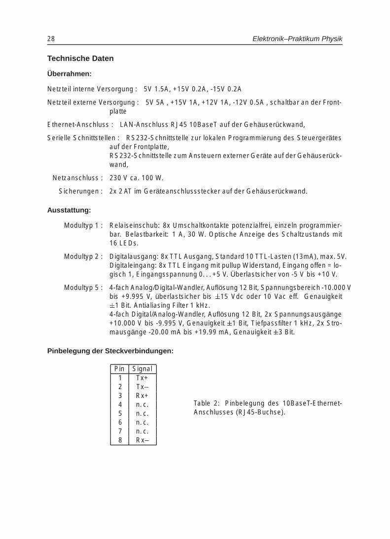
Pinbelegung der Steckverbindungen:
Pin Signal1 Tx+2 Tx–3 Rx+4 n. c.5 n. c.6 n. c.7 n. c.8 Rx–
Table 2: Pinbelegung des 10BaseT-Ethernet-Anschlusses (RJ45-Buchse).

Measurement and Control System 29
Pin Signal1 DCD2 RxD3 TxD4 DTR5 Gnd6 DSR7 RTS8 CTS9 n. c.
Table 3: Pinbelegung der RS232-Anschlüsse(9-polige Sub-D-Stecker). Alle Handshake-Leitungen (DCD, DTR, DSR, RTS, CTS) sindauf logisch TRUE (+10 V) gesetzt. TxD undRxD können durch interne Steckbrücken ver-tauscht werden.
a c+5V Logic � 1 � +5V Logic
Data Bus D7 � 2 � Data Bus D6Data Bus D5 � 3 � Data Bus D4Data Bus D3 � 4 � Data Bus D2Data Bus D1 � 5 � Data Bus D0
0V Logic Ground � 6 � 0V Logic GroundAddress Bus A6 � 7 � Address Bus A5Address Bus A4 � 8 � Address Bus A3Address Bus A2 � 9 � Address Bus A1Address Bus A0 �10 � n. c.
n. c. �11 � n. c.n. c. �12 � n. c.n. c. �13 � n. c.n. c. �14 � n. c.
Address Bus A7 �15 � Management Bus RD#Management Bus SD3 �16 � Management Bus WR#Management Bus SD2 �17 � Management Bus BEN#Management Bus SD1 �18 � Management Bus BDIRManagement Bus SD0 �19 � n. c.
+5V Power �20 � +5V Power+5V Power �21 � +5V Power
0V Power Ground �22 � 0V Power Ground0V Power Ground �23 � 0V Power Ground
n. c. �24 � n. c.n. c. �25 � n. c.
+15V Analog �26 � +15V Analog+15V Analog �27 � +15V Analog–15V Analog �28 � –15V Analog–15V Analog �29 � –15V Analog
0V Analog Ground �30 � 0V Analog Ground0V Analog Ground �31 � 0V Analog Ground0V Analog Ground �32 � 0V Analog Ground
Table 4: Pinbelegung am 64-poligen Peripheriebus.

30 Elektronik–Praktikum Physik
Anhang B: Schaltpläne
Anhang Schaltpläne und Messprotokolle
Universität Osnabrück, FB Physik, Elektronikwerkstatt, Postfach 4469, D-49069 Osnabrück
GerätGeräteteil
AuftragsdatenAuftraggeber
Inv. / Kostenst.
Blatt 1
vonTechniker M.Dr
Konstr.Archiv S 93 - 505
0420
K. Betzler20000911
SC12 Prozessor
Rev. 3
Ra
15.05.01Datum
: Steuergerät f. E-Prakt.
Universität Osnabrück, FB Physik, Elektronikwerkstatt, Postfach 4469, D-49069 Osnabrück
GerätGeräteteil
Auftragsdaten
AuftraggeberInv. / Kostenst.
Blatt 2
vonTechniker M. Dr
Konstr.
Archiv S93 - 5050420
K. Betzler20000911
Digital In/Out
Rev. 3
Ra
15.05.01Datum
: Steuergerät f. E-Prakt.

Measurement and Control System 31
Universität Osnabrück, FB Physik, Elektronikwerkstatt, Postfach 4469, D-49069 Osnabrück
GerätGeräteteil
AuftragsdatenAuftraggeberInv. / Kostenst.
Blatt 3
vonTechniker M. Dr
Konstr.Archiv S93 -555
0420
K. Betzler20000911
Relaisausgang
Rev. 3
Ra
15.05.01Datum
: Steuergerät f. E-Prakt.
Universität Osnabrück, FB Physik, Elektronikwerkstatt, Postfach 4469, D-49069 Osnabrück
GerätGeräteteil
AuftragsdatenAuftraggeber
Inv. / Kostenst.
Blatt 5
vonTechniker M. Dr
Konstr.Archiv S93 -505
0420
K. Betzler20000911
Frontansicht
Rev. 2
Ra
12.12.00Datum
: Steuergerät f. E-Prakt.

32 Elektronik–Praktikum Physik
Uni
vers
itätO
snab
rück
,FB
Phys
ik,E
lekt
roni
kwer
ksta
tt,P
ostf
ach
4469
,D-4
9069
Osn
abrü
ck
GerätGeräteteilAuftragsdaten
AuftraggeberInv. / Kostenst.
Blatt 4von
Techniker M. DrKonstr.
Archiv S 93 -5050420
K. Betzler20000911
AD/DA Wandler Einschub
Rev. 3
Ra
15.05.01Datum
: Steuergerät f. E-Prakt.

Measurement and Control System 33
Universität Osnabrück, FB Physik, Elektronikwerkstatt, Postfach 4469, D-49069 Osnabrück
GerätGeräteteil
AuftragsdatenAuftraggeber
Inv. / Kostenst.
Blatt 6
vonTechniker M. Dr
Konstr.Archiv S 93 -505
0420
K. Betzler20000911
Rückwand
Rev. 2
Ra
12.12.00Datum
: Steuergerät f. E-Prakt.