Embed Size (px)
Citation preview

Ka-band Full Duplex System with Electrical Balance Duplexer
For 5G Applications using SiGe BiCMOS Technology
by
Alper Güner
Submitted to the Graduate School of Engineering and Natural Sciences
In partial fulfillment of
The requirements for the degree of
Master of Science
Sabanci University
Summer, 2018
ii

iii
© Alper Güner 2018
All Rights Reserved

iv
Acknowledgements
I would like to thank my supervisor Prof. Dr. Yaşar Gürbüz for his invaluable
guidance and support throughout my undergraduate and master’s years.
I would like to thank the members of my thesis committee, Assist. Prof.
Erdinç Öztürk and Assoc. Prof. Burak Kelleci for their helpful comments and
for their time.
I am thankful to my wife and my family for always helping and supporting me
in every possible way.
I also would like to express my special thanks to my friends Abdurrahman
Burak, Atia Shafique, Can Caliskan, Cerin Ninnan, Elif Gül Arsoy, Emre Can
Durmaz, Eşref Türkmen, Hamza Kandiş, İlker Kalyoncu, Melik Yazici, Omer
Ceylan and Shahbaz Abbasi who made my master’s studies so enjoyable.
Finally, I want to thank my friends Didem Koçhan and Ahmet Can Mert for
all their help and support.

v
Ka-band Full Duplex System with Electrical Balance Duplexer
For 5G Applications using SiGe BiCMOS Technology
Alper Guner
EE, Master’s Thesis, 2018
Thesis Supervisor: Prof. Dr. Yasar GURBUZ
Keywords: Transceiver, Single Antenna, Full Duplex, Hybrid Transformer, Impedance
Tuner, SiGe BiCMOS, Ka-band Integrated Circuits
ABSTRACT
The current dominating communication system is 4G. However, with the increase in
the data rate and in the number of users in the world, the 4G communication system has
started to saturate and couldn’t manage to keep up with user demands and there is less
room for progress at 4G systems. In search of finding a system that covers the future
interests of users, a new communication scheme is being processed as 5G. The next
generation systems require wider bandwidth, high spectral efficiency, and less latency. For
these goals, designs with higher frequency and full-duplex operation mode have been
started to gain attention. Developments in SiGe HBT technologies -higher fT and fmax-
make them suitable for these challenges. Considering these trends which lead to the future
of communication systems, in this thesis the design of Ka-band (25-32GHz) SiGe full
duplex system with electrical balance duplexer for 5G applications is presented. This
system is created by integrating. a duplexer, an LNA, and a PA.
The electrical balance duplexer is realized by a hybrid transformer and a balancing
network. The impedance of the antenna is mimicked by tuning the balancing network to
provide high isolation between transmitter and receiver blocks. All the ports have better
than 10dB return loss. Duplexer provides measured 39dB peak isolation at 28GHz, with
3.8dB insertion loss from the transmitter to the antenna and 4.7dB insertion loss from the
antenna to receiver. The LNA achieves the measured gain of 15dB, NF of 3.5dB and
OP1dB of 13.5dBm at 28GHz by including an input and an output BALUN transformer.
The PA provides measured gain of 17dB and OP1dB of 14dBm at 28GHz.

vi
5G Kullanım Alanları için SiGe BiCMOS
Ka-bandında Tam Dupleks Sistem
Alper Güner
EE, Yüksek Lisans Tezi, 2018
Tez Danışmanı: Prof. Dr. Yasar GÜRBÜZ
Keywords: Alıcı-verici Devreleri, Tek Anten, Tam Dupleks, Hibrit Dönüştürücü,
Empedans Ayarlayıcı, SiGe BiCMOS, Ka-bandında entegre devre
ÖZET
Günümüzde hakim olan iletişim sistemi 4G'dir. Veri kullanımdaki ve dünyadaki
kullanıcı sayısındaki artışla birlikte, 4G iletişim sistemi kullanıcıların isteklerine karşılık
verememeye başlamıştır ve 4G teknolojilerinde gelişimin sonuna gelmiştir. Kullanıcıların
gelecekteki isteklerini kapsayan bir sistem bulmak için, yeni bir iletişim sistemi
geliştirilmelidir ve bu sistem 5G olarak belirlenmiştir. Yeni nesil sistemler daha yüksek
bant genişliği, yüksek spektral verimlilik ve daha az gecikme gerektirmektedir. Son
yıllarda, bu hedefler için daha yüksek frekanslı ve tam dupleks modlu tasarımlar ilgi
toplamaya başlamıştır. SiGe HBT teknolojilerindeki gelişmeler -daha yüksek fT ve fmax- bu
teknolojiyi yeni nesil tasarımlara uygun hale getirmiştir. Haberleşme sistemlerinin
geleceğine yön veren bu eğilimler göz önünde bulundurularak, bu tez, 5G uygulamaları için
elektrik dengesi duplekseri ile Ka-band (25-32GHz) SiGe tam dupleks sisteminin
tasarımını sunmaktadır. Bu sistem bir dupleksleyici, bir LNA ve bir PA’den oluşmaktadır.
Elektriksel denge dupleksleyici bir hibrit transformatör ve bir dengeleme ağı ile
tasarlanmıştur. Verici ve alıcı blokları arasında yüksek izolasyon sağlamak için anten
empedansının dengeleme ağının ayarlanmasıyla takip edilmesi gerekmektedir. Tüm portlar
10dB’den daha iyi geri dönüş kaybına sahiptir. Dupleksleyicinin vericiden antene simüle
edilmiş kaybı 3.8dB, antenden alıcıya simüle edilmiş kaybı ise 4.7dB’dir. 28 GHz'de 39 dB
maksimum izolasyon sağlamaktadır. LNA, giriş ve çıkış BALUN transformatörleri içerir
ve ölçülmüş sonuçları 28GHz'de 15dB kazanç, 3.5dB'lik NF ve 13.5dBm'lik OP1dBdir.
PA, 28GHz'de 17dB kazanç sağlar ve 14dBm'lik OP1dB çıkış gücüne ulaşmaktadır.

vii
Contents
Acknowledgements iv
Abstract v
Özet vi
Contents vii
List of Figures ix
List of Tables xii
List of Abbreviations xiii
1 Introduction ................................................................................................................... 1
1.1 5G ............................................................................................................................. 1
1.2 Duplexing ................................................................................................................. 3
1.3 SiGe/BiCMOS Technology ..................................................................................... 6
1.4 Motivation ................................................................................................................ 9
1.5 Organization ........................................................................................................... 10
2 Fundamentals of Duplexers ....................................................................................... 11
2.1 Introduction ............................................................................................................ 11
2.2 Duplexers ............................................................................................................... 11
2.2.1 Circulators ....................................................................................................... 13
2.2.2 Orthomode Transducer ................................................................................... 14
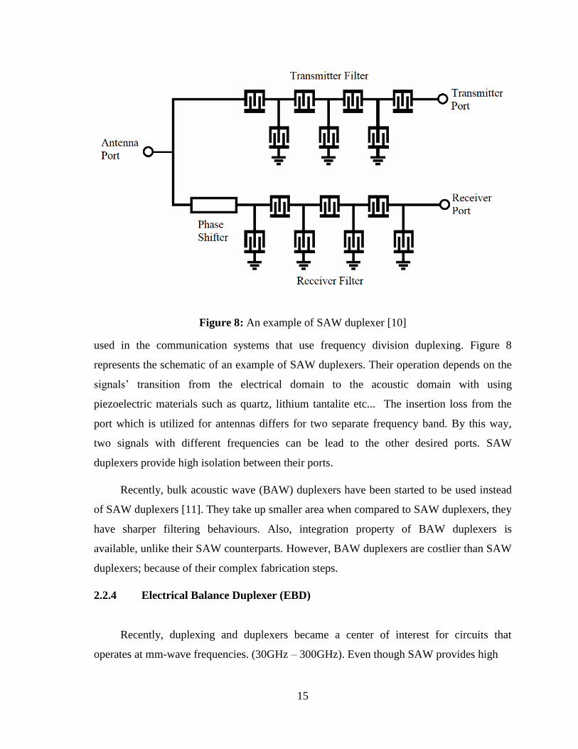
2.2.3 Surface Acoustic Wave (SAW) Duplexers ..................................................... 14
2.2.4 Electrical Balance Duplexer (EBD) ................................................................ 15
2.3 Transformers .......................................................................................................... 17
2.4 Hybrid Transformers .............................................................................................. 19
2.4.1 Bi-Conjugacy of Hybrid Autotransformers .................................................... 22

viii
2.4.2 Power Splitting of Hybrid Transformers ........................................................ 24
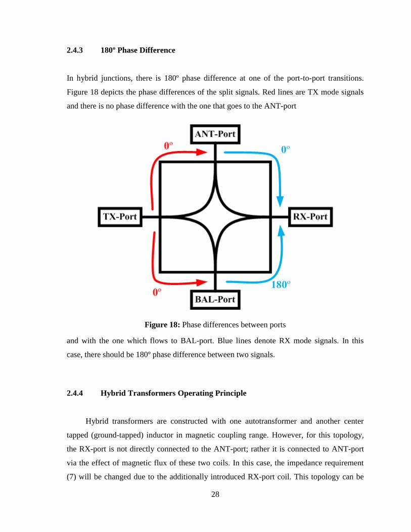
2.4.3 180º Phase Difference ..................................................................................... 28
2.4.4 Hybrid Transformers Operating Principle ...................................................... 28
2.5 Balancing Network ................................................................................................. 32
3 Full Duplex System with Electrical Balance Duplexer ............................................ 34
3.1 Introduction ............................................................................................................ 34
3.2 EBD Design ........................................................................................................... 35
3.2.1 Hybrid Transformer Design ............................................................................ 35
3.2.2 Impedance Tuner ............................................................................................ 45
3.3 LNA Design ........................................................................................................... 54
3.4 PA Design .............................................................................................................. 62
3.5 Full Duplex System ................................................................................................ 66
3.6 Comparison ............................................................................................................ 71
4 Conclusion & Future Work ....................................................................................... 73
4.1 Summary of the Work ............................................................................................ 73
4.2 Future Work ........................................................................................................... 74
5 References .................................................................................................................... 75

ix
List of Figures
Figure 1: Mobile data traffic growth in 2016 [2] ................................................................... 2
Figure 2: a) Block diagram of TDD b) Block diagram of FDD ............................................ 4
Figure 3: Depiction of working principal of a) TDD b) FDD c) IBFD ................................. 4
Figure 4: Cross section of IHP 0.13µm SiGe HBT Technology [24] ................................... 9
Figure 5: Block diagram of transceivers with duplexers ..................................................... 11
Figure 6: Block diagram of the circulators (clock-wise operation) ..................................... 13
Figure 7: Fabricated orthomode transducers [9] .................................................................. 14
Figure 8: An example of SAW duplexer [10] ..................................................................... 15
Figure 9: Block diagram of EBD's....................................................................................... 16
Figure 10: Schematic of a transformer ................................................................................ 18
Figure 11: Hybrid transformer as duplexer ......................................................................... 20
Figure 12: Schematic of an autotransformer ....................................................................... 20
Figure 13: Double tapped autotransformer .......................................................................... 21
Figure 14: Currents in TX-RX bi-conjugacy analysis ......................................................... 22
Figure 15: Currents in ANT-BAL bi-conjugacy analysis .................................................... 24
Figure 16: Power splitting ratios of an EBD ....................................................................... 25
Figure 17: TX and RX insertion loss values with respect to changing power ratio ............ 27
Figure 18: Phase differences between ports ........................................................................ 28
Figure 19: Hybrid transformer and currents ........................................................................ 29
Figure 20: Common mode signals in TX mode ................................................................... 30
Figure 21: Differential signals in RX mode ........................................................................ 31
Figure 22: Block diagram of full-duplex core circuitry ....................................................... 34
Figure 23: Schematic model of a transformer [16] .............................................................. 37
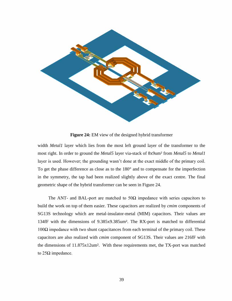
Figure 24: EM view of the designed hybrid transformer .................................................... 39
Figure 25: Simulated reflection coefficient seen from ports of hybrid transformer a) dB
scale b) Smith Chart representation ...................................................................................... 40
Figure 26: Simulated TX-RX isolation with fixed resistances at ANT- and BAL-port ...... 40
Figure 27: Simulated TX- to ANT-port and ANT- to RX-port insertion loss values .......... 41

x
Figure 28: Simulated phase difference between two differential terminals of RX-port ...... 41
Figure 29: Chip photo of fabricated hybrid transformer combined with BALUN
transformer ............................................................................................................................ 43
Figure 30: Measured S11 and S22 behavior of the hybrid transformer-BALUN structure 44
Figure 31: Measured TX-RX isolation value of the hybrid transformer-BALUN structure
.............................................................................................................................................. 44
Figure 32: a) Layer view of the MOM capacitor b) Comparison of MOM capacitor with
ideal component .................................................................................................................... 47
Figure 33: Isolated NMOS cross-section ............................................................................. 48
Figure 34: Schematic of impedance tuner block ................................................................. 48
Figure 35: Layout of the impedance tuner ........................................................................... 49
Figure 36: Chip photo of the impedance tuner .................................................................... 51
Figure 37: Simulated impedances swept by an individual variable capacitor bank ............ 52
Figure 38: Comparison of a) measured and b) simulated impedance values for states of the
balance network .................................................................................................................... 52
Figure 39: Chip photo of the fabricated EBD ...................................................................... 53
Figure 40: Simulated values of TX- to RX-port isolation for each state of the tuner ......... 53
Figure 41: Schematic of the LNA design ............................................................................ 56
Figure 42: Chip photo of fabricated LNA ........................................................................... 58
Figure 43: NF measurement setup for LNA ........................................................................ 58
Figure 44: OP1dB measurement setup for LNA and PA .................................................... 59
Figure 45: Measured S11 and S22 behavior of the designed LNA ..................................... 59
Figure 46: Measured gain of the designed LNA ................................................................. 60
Figure 47: Measured NF performance of the designed LNA .............................................. 60
Figure 48: Measured 1dB compression point of the designed LNA ................................... 61
Figure 49: Simulated IIP3 value of the LNA w/o input BALUN ........................................ 61
Figure 50: Schematic of the PA design ............................................................................... 63
Figure 51: Chip photo of the fabricated PA ......................................................................... 64
Figure 52: Measured S11 and S22 behavior of the designed PA ........................................ 64
Figure 53: Measured gain performance of the designed PA ............................................... 65
Figure 54: Measured 1dB compression point of the designed PA ...................................... 65

xi
Figure 55: Chip photo of the full-duplex system ................................................................. 66
Figure 56: Measured input and output reflection coefficients of TX-ANT path ................. 67
Figure 57: Measured gain of TX-ANT path ........................................................................ 68
Figure 58: Output power graph of TX-ANT path with respect to input power ................... 68
Figure 59: Simulated input and output return losses of the ANT-RX path ......................... 69
Figure 60: Simulated gain performance of the ANT-RX path ............................................ 70
Figure 61: Simulated NF behavior of the ANT-RX path .................................................... 70
Figure 62: Simulated 1dB compression point performance of the ANT-RX path .............. 71

xii
List of Tables
Table 1: Comparison of different integrated circuit technologies with respect to different
performance metrics (++: Very good, +: Good, 0: Average, -: Decent, --: Poor)…………...7
Table 2: Comparison 5G full-duplex system with other reported works………………….72

xiii
List of Abbreviations
ADC Analog-to-Digital Converter
ANT Antenna
BAL Balance
BALUN Balance-to-Unbalance
BAW Bulk Acoustic Wave
EBD Electrical Balance Duplexer
ESD Electro-statical Discharge
ENR Excess Noise Ratio
4G Fourth Generation Mobile Phone Standards
FDD Frequency Division Duplex
FD Full Duplex
GaAs Gallium Arsenide
HBT Hybrid Bipolar Junction Transistor
IBFD In-Band Full Duplex
InP Indium Phosphate
IOT Internet of Things
LNA Low Noise Amplifier
MIM Metal-Insulator-Metal
mmWave Millimeter Wave
MIMO Multiple Input Multiple Output
NF Noise Figure
OP1dB Output 1dB Compression Value
PA Power Amplifier
RX Receiver
SPI Serial-to-Parallel Interface
SiGe Silicon Germanium
SPDT Single-Pole Double Throw
SAW Surface Acoustic Wave

xiv
TDD Time Division Duplex
TX Transmitter


1
1 Introduction
1.1 5G
Wireless technologies and communication system had become mainstream for people
a long time ago. They took a great place in every aspect of life such as high-quality data
transfer, cloud operations, vehicle-to-vehicle or vehicle-to-infrastructure communication,
virtual/augmented reality applications, automation of industrial devices, smart
houses/cities, personal healthcare applications and the unlimited number of examples can
be given for applications of the wireless systems. From the emerging point of
telecommunication until now; there is a rapid improvement and development in the field of
communication systems. During this period, communication systems completely evolved
and changed not once but several times [1].
Today the most recent technology is the fourth-generation mobile phone standards
(4G). For instance; today, with 4G’s high data transfer rate, it is providing high-quality
video and audio streaming. However; even 4G structures can’t handle today’s user demand
and there is only fractional room is left for development. The most important problem for
4G is the increase in both demand and device numbers. The demand for data is growing not
linearly but exponentially with each year. From 2015 to 2016, mobile data transfer rate is
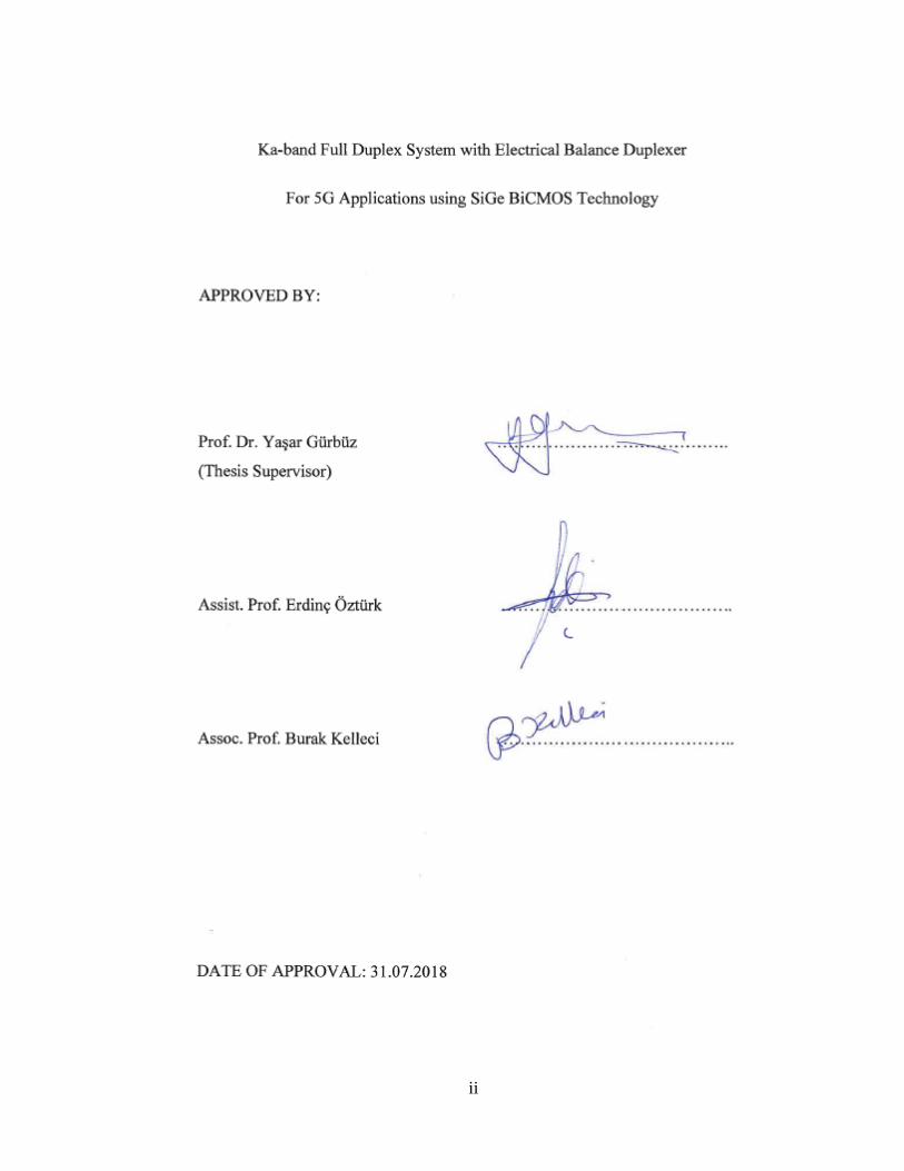
increased by 63% from 4.4 exabytes to 7.2 exabytes. The data transfer growth in 2016 can
be seen in Figure 1. Also, the number of active devices raised from 7.6 billion to 8 billion
in only one year. In 2021, the expected number of mobile devices is 11.6 billion [2]. The
disadvantages of 4G can be explained as follows: Firstly, even though 4G has a large
bandwidth, they are not used by all of the world. These bandwidths are specialized to
different locations and mobile devices can’t operate in every single one of them due to the
electronic component limitation. Secondly, the 4G communication system is not
compatible with Wi-Fi structures. Being suitable with Wi-Fi technology could create great
benefits for bandwidth and it would relax the bandwidth requirements. Also, with the
introduction of more and more internet of things (IoT) devices to the market, wireless
systems became more important. Finally, 4G will not be able to provide the sufficiently low
latency values (~1ms) especially for IoT devices [3].
2
Figure 1: Mobile data traffic growth in 2016 [2]
Until now 4G met the demands of the users; however, due to the reason that has been
mentioned above, the technology needed a brand-new communication system called 5G.
While thinking about the requirements of 5G structure, the inadequacies of the 4G system
can be taken as references. First one is latency and the second one is cost and efficiency.
The last and most important of the requirements is the high data rate. 5G is promising the
data rate which thousand times of 4G. One of the key steps that make this available is
increasing the operation frequencies of the communication systems. The frequency
spectrum that is common today is almost full and communication requires new bandwidth.
It is the most effective way to provide large bandwidth for the users. For this purpose,
millimeter wave (mmWave) frequencies come into consideration. However, these
frequencies were not thought of as suitable for communication systems. Basically, because,
they are hard to propagate. Few of the reasons for this property can be given as path loss,
low penetration to walls, atmospheric and rain absorption [4]. In recent years, several
different ways to overcome these problems emerged. For example, keeping the antenna
sizes which are used for smaller frequencies may be a solution for higher frequency
applications. These large arrays can eliminate the frequency dependence of the propagation
path loss. Another way can be smaller cells with narrower beams with their low

3
interference behavior [5]. An additional challenge with working at higher frequency is how
can the integrated circuit technology satisfy the high-frequency operation. As the size of the
chips becomes smaller and smaller, and as the fT’s of the transistor becomes higher, the
complexity of chip fabrication increases drastically and this leads to the higher prices for
the production of circuits.
1.2 Duplexing
Apart from higher spectrum range; another important aspect of communication with
the increase in user and devices numbers is the spectral efficiency. Today, the most
common way of how designers use the communication systems is half-duplexing which
means that using the same antenna for transmitting or receiving the signals but not
concurrently or with the same frequency. Receiving and transmitting operations happen one
at a time. This operation is named as time division duplexing (TDD). Generally, there is a
single pole double throw (SPDT) switch placed between the antenna and
transmitter/receiver. In one operation mode of the SPDT; while receiver block is active,
transmitter operation is suppressed. In the other mode of SPDT, the operations will be
reversed. Another common method is using frequency division duplexing (FDD). Also, in
this case, the same antenna is used for both operations; however, with different frequency
values. These two different frequency values enable using different filters between antenna
and transmitter/receiver blocks. Transmitter signal converted into a signal that the receiver
can detect in base stations. The working principle of TDD and FDD can be seen in Figure
2.
As explained before, both TDD and FDD are working on half-duplex mode.
However, in this condition, the resources can’t be used at their full efficiency potential.
Therefore, designers started to consider systems that able concurrent transmit and receive
operations with the same frequency band; in order to increase the spectral efficiency when
compared to half-duplex systems. These structures are named as full-duplex (FD) or in-
band full duplex (IBFD) systems. Being able to transmit and receive at the same time with
the same frequency band, is theoretically doubling the spectral efficiency of the system
when compared to half-duplex systems.

4
Figure 2: a) Block diagram of TDD b) Block diagram of FDD
Figure 3: Depiction of working principal of a) TDD b) FDD c) IBFD
Figure 3 shows the type of operation in TDD, FDD and IBFD systems with respect to
time. In this figure, green blocks show the transmit operation and blue blocks denote the
receive operation. As explained before; in TDD systems, transmit and receive operations
are controlled with an SPDT switch and they are working in order. There is a gap between
each operation because of the delays in the switch and also to ensure that system is working
in a safe manner. In FDD systems, they operate the incoming and outgoing signals at the
same time but with different frequencies. Lastly, for IBFD both transmit and receive signal
-with the same frequency- is processed concurrently. With using same frequency bands, FD
systems do not consume frequency space like FDD systems. This creates opportunity for
other applications to use those unused frequency bands. Properties of IBFD’s like increased

5
spectral efficiency and generous usage of frequency bands, full-duplex systems become
suitable for 5G applications; because of the requirements mentioned above.
Another design necessity of 5G operations is decreased latency in operations such as
IoT devices. Since there is no switch between antenna and circuits in FD systems, there is
no need to divide the operation into time steps. This will lead to decrease in latency.
Another benefit provided with this property is that there will be no package collision.
Because, a received signal can still be detected while the system is transmitting. Small cells
with massive multiple-input multiple-output (MIMO) systems will be important structures
for 5G applications. This will also increase the channel capacity. Using one antenna while
maintaining both operations concurrently will make FD systems suitable for MIMO
structures.
Although FD systems provide higher spectral efficiency; they have some drawbacks
and challenges. In FD systems, there is a huge self-interference from structure’s own
transmit blocks to the receiver. If this self-interference is not dealt with, the channel
capacity of the FD system can even fall behind of their HD counterparts. This interfered
signal is large in amplitude when compared to receiver’s input signal at any given time.
This behavior can cause degradation in the sensing performance of receivers, because the
received signal will be negligible against that self-interference signal. It is considered as
canceling can be achieved by subtracting this signal from itself. However, this approach is
not feasible. For instance, if this cancellation is wanted to be done in digital domain, the
amount of dynamic range required for analog-to-digital converters (ADC) will be high. For
cancellation in RF domain; oscillator phase noise and sub-block’s non-linearities will create
problems. So, for years, designers have searched for other ways to cancel the self-interfered
signal. These applications can be classified into two sections: passive cancellation and
active cancellation. Passive cancellation includes directional suppression (the radiation
lobes of transmit and receive operations are separated) and antenna separation (increasing
the loss between transmit and receive antennas). Active cancellation is achieved through
analog cancellation (a copy of transmit signal is obtained and with correct amplitude and
phase values, it is cancelled with receiver port) and digital cancellation in the digital
domain. However, all of these applications have their flaws and couldn’t meet the desired
specifications for 5G full-duplex operations [6]. Using duplexer between antenna and

6
transmit/receive modules provides non-complex, cheap, and effective way to cancel the
interfered transmitter signal.
1.3 SiGe/BiCMOS Technology
Today, integrated circuit industry dominated by three fabrication processes and
technologies. These are III-V group technology, CMOS and SiGe/BiCMOS. Almost all the
integrated circuit such as transceivers are realized using these processes. When compared
between them, III-V technology is the oldest and most mature technology of all. III-V
transistors such as gallium arsenide (GaAs) or indium phosphate (InP) have the best
performance with respect to other -in gain, noise figure and most importantly output power
aspects-. Most of the applications that require very high output power are realized with
power amplifiers whose transistors belong to III-V technology.
Another important positive side this technology is very small process variations. Even
though III-V group fabrication results in best performance, there are severe drawbacks that
make this technology unfavorable in various situations. This technology is expensive when
compared to other processes. Also, integration possibility with digital domain is non-
existing. These problems make III-V group technologies less appealing and create demand
for other fabrication processes.
Until now, CMOS technology stayed behind from other processes in performance;
however, with the recent developments, it started to show comparable performance with
others. CMOS technology offers little lower performance with cheaper fabrication. CMOS
technology also dominates the digital integrated circuit domain today with smaller gate
sizes almost every 2 years. The downside of CMOS technology is the process variations.
The performances of the transistors or the values of passive structures may differ from
process to process. The expected simulated results can’t be acquired consistently with this
technology.

7
Table 1: Comparison of different integrated circuit technologies with respect to different
performance metrics (++: Very good, +: Good, 0: Average, -: Decent, --: Poor) [23]
Performance
Metric
SiGe
HBT
SiGe
BJT
Si
CMOS
III-V
MESFET
III-V
HBT
III-V
HEMT
Frequency Response + 0 0 + ++ ++
1/f and Phase Noise ++ + - -- 0 --
Broadband Noise + 0 0 + + ++
Linearity + + + ++ + ++
Output Conductance ++ + - - ++ -
Transconductance ++ ++ -- - ++ -
Power Dissipation ++ + - - + 0
CMOS Integration ++ ++ N/A -- -- --
IC Cost 0 0 + - - --
Lastly, SiGe/BiCMOS technology stay at the middle of these two technologies in
both by performance and cost senses. With improvements in the technology,
SiGe/BiCMOS comes into a place that it can race with the performance of III-V. Although
it is expensive from CMOS technology with a little margin, SiGe/BiCMOS is greatly
cheaper than III-V. Another upside of SiGe is its integration possibility with digital domain.
Also, the process variations and yield number for this technology is greater than its CMOS
counterpart. Today, in the literature, there can be found integrated circuit studies with state-
of-the-art performance values which are utilized with silicon germanium heterojunction
bipolar transistors (SiGe HBT) of the SiGe/BiCMOS technology.
While selection of the technology for aimed operation, a series of important
specifications of a process should be considered. Two important points of these properties
are fT and fMAX of the transistors of the technology. fT is the cut-off frequency of a given
transistor. It shows the frequency which at current gain (β) of the transistor is unity. fMAX is
the maximum oscillation frequency of a transistor. It represents the frequency where power
gain of the transistors becomes unity. These two values are important especially for the
high frequency integrated circuit applications such as 5G communication systems; because

8
with higher fT and fMAX values, transistors provide more gain and low noise figure values at
the higher frequencies.
In order to increase the performance of the transistor, bandgap engineering is applied
to the bases of the HBT’s. To realize the bases of those transistors SiGe alloys are grown
epitaxially. While silicon has the bandgap voltage of 1.12eV, germanium’s is only at
0.66eV. By using a material with smaller bandgap voltage than silicon, electron injection is
increased; therefore, the current gain of the transistors. Germanium does not only increase
the β but also creates electric field inside of the transistor. This leads to an increment in the
speed of the carriers in other words effecting base-transit time (τB). All of these aftermaths
of introducing germanium doping to the silicon improves the fT of the transistors. Relation
can be seen in the following equation.
𝑓𝑇 = 1
2𝜋(𝜏𝐵 + 𝜏𝐶 +
1
𝑔𝑚(𝐶𝜋 + 𝐶𝜇) + (𝑟𝑒 + 𝑟𝑐)𝐶𝜇)
−1 (1)
Where the τC denotes the collector transit time, gm is the transconductance, Cπ and Cµ
are the parasitic capacitances from base to emitter and base to collector, respectively and
lastly, re and rc are parasitic resistances at emitter and collector, in order. As can be seen at
the (1) fT performance of transistors increases with lower τB and higher gm. As highlighted
before, another important metric for transistors is fMAX. Its formulization can be given as
following.
𝑓𝑀𝐴𝑋 = √𝑓𝑇
8𝜋𝐶𝜋𝑟𝑏 (2)
Where rb is the parasitic base resistance. Germanium doping to the silicon decreases
the parasitic base resistance without affecting current gain in a bad manner; therefore,
transistors with germanium doping provides better noise performance when compared to
their Si counterparts. In short, germanium doping to the base of the transistors improve
every single important performance specification of the transistors.

9
Figure 4: Cross section of IHP 0.13µm SiGe HBT Technology [24]
Today, applications that require ultra-high accuracy and performance, such as
military purposes, are still using III-V technology; because in those domains, expenses and
integration properties are secondary concerns. Unlike III-V, SiGe is more favorable for
commercial usages such as communication systems, short range vehicular radars, RFIDs,
and biological research. To summarize, SiGe/BiCMOS offers good performance with
excellent cost and integration properties. With SiGe/BiCMOS fully integrated system-on-
chip devices can be realized in microwave and mm-Wave frequencies with low cost and
high performance.
1.4 Motivation
With the increase in demand for higher data rate and efficient usage of frequency
spectrum, 5G and full-duplex concepts started to gather attention by both academia and
10
industry, because they carry the possibility of effecting every aspect of daily or domain
specific aspects of people’s life by creating powerful, efficient and fast transceivers.
Current applications of duplexing are generally done with bulky, complex, non-flexible and
expensive components. Also, the integration problems are severe. Recently, integrated
tunable duplexers got popular in designs. On-chip, tunable duplexers have huge challenges
in their designs, yet, they can lead to cheaper and effective solutions.
The objective is this thesis is to design a core chip block prototype for in band full-
duplex operated transceiver modules, which operates between Ka-band for 5G applications
with using IHP 0.13µm SiGe/BiCMOS technology. This core chip includes an on-chip
hybrid transformer, a balancing network, a low noise amplifier and a power amplifier. This
thesis aims to present the design steps of these blocks and discuss/analyze the measurement
result for each block and whole system as well.
1.5 Organization
This thesis is organized as follows: Chapter 2 explains the fundamentals of the
duplexer theory by giving the meaning of the duplexing with duplexer types first. Then
electrical balance duplexers are analyzed from the basic of transformers and hybrid-
transformer necessities. Lastly, balance networks and their properties are explained.
Chapter 3 starts with design considerations for full-duplex stroke. First, design steps
of hybrid transformer are explained. Second, the balance network which help hybrid
transformer while operating as a duplexer is discusses. Other blocks of the system -PA and
LNA- are stated. All of these blocks simulation and measurement results are shown in
Chapter 3. The proposed system is shown and the measurement results are represented and
explained. Lastly, the performance of the full-duplex system is compared with other
reported works.
Finally; chapter 4 gives a summary of the thesis and discusses some other challenges
that are encountered through designs. Also, possible future variations and designs on this
topic are discussed.

11
2 Fundamentals of Duplexers
2.1 Introduction
In this chapter, the fundamental properties of the duplexers are explained. First, the
purpose of the duplexers is discussed with the basic performance necessities for reasonable
operation. Secondly, different types of duplexers are covered, and their
advantages/disadvantages are discussed. Then, with the basics of transformer design,
hybrid transformers are analyzed through their three important metrics in order. This starts
with bi-conjugacy between the ports of the hybrid transformers and continues with the
power splitting and 180º phase shift properties with using auto-transformer theory.
2.2 Duplexers
Figure 5: Block diagram of transceivers with duplexers

12
Duplexing means using the same antenna for both transmit and receive operations.
Duplexing is achieved via duplexers which are one of the most essential sub-blocks of the
communication and the radar systems which operates in almost all the frequency bands.
Duplexers are used just before the antennas in order to use the same antenna for both
transmitted and received signal as can be seen from Figure 5 while blue arrows denote the
signal flowing from the transmitter block to the antenna, green arrows depict the received
signal which is coming from the antenna, red line shows the leakage signal from the end of
the transmitter to the receiver side and finally black arrows shows the transmitted and
received signals by the antenna. However; even though duplexers enable designers to use
the same antenna for both transmit and receive mode, there are challenges in duplexer
design and they need crucial specifications to be operable in transceiver modules.
First of all, while providing simultaneous operation with one antenna, duplexers need
to prevent out-of-band signals to propagate to the system. Secondly, due to their positions
in transceiver modules, their performance is affecting the specifications of the systems,
severely. The loss that is introduced from antenna to receiver, directly adds up to the noise
figure performance. Also, the loss that comes from transmitter to antenna connection is
degrading the signal power that arrives at the antenna. Another necessity for the duplexers
is their power handling capacities. Duplexers must be able to work on high power signals
and shouldn’t add any non-linearities that will deteriorate the performance while operating
at high power. Lastly; and most importantly; a duplexer should provide high isolation
between the output of the transmitter and the input of the receiver in a relatively wide signal
bandwidth. Due to the imperfections, there will be signal leakage from the transmit side to
the receiver. If this leakage can’t be blocked or canceled out by the duplexer, it will distort
the incoming signal to the receiver and even saturate the LNA input which damages the
linearity. In order to duplex the systems, several different methods have been used to this
date; such as circulators, orthomode transducers, surface acoustic wave (SAW) filters,
electrical balance duplexers (EBD).

13
Figure 6: Block diagram of the circulators (clock-wise operation)
2.2.1 Circulators
Circulators are non-reciprocal components that have 3-ports and transfer signal in
clockwise or counter clockwise directions as can be seen in Figure 2 while the arrows
depict the direction of propagating signals in a circulator. In other words (for clockwise
rotation); a signal from Port-A will only flow to Port-B, a signal from Port-B will only flow
to Port-C and finally a signal from Port-C will only flow to Port-A. For transceiver
applications, an antenna can be connected to the Port-B, transmitter circuitry can be
connected to Port-A and receiver block can be connected to Port-C. By this way, the
duplexing operation can be achieved. However, any reflected signal from the entrance of
the receiver can leak to the transmitter and deteriorate the overall system performance so it
should be considered in designs. The important design metrics of the circulators are high
isolation and low insertion loss between ports.
Circulators can be used as external ferrite-based circulators or as on-chip quasi-
circulators in full duplex transceiver systems [7], [8]. Even though external circulators have
low loss property, they are bulky, expensive, non-flexible and non-integrable. On-chip

14
Figure 7: Fabricated orthomode transducers [9]
circulators provide compact and low-cost designs, but they come with high insertion loss
between the ports and narrow-band operation drawbacks.
2.2.2 Orthomode Transducer
Orthomode transducers are waveguide components and can be used as duplexers in
transceiver systems and an example to them can be seen in Figure 7. Their behavior
depends on the polarization of the signals. Orthomode transducers are separating two
signals with the same frequency but with different orthogonal polarizations. This property
can lead to the full duplex usage of a transceiver system. Orthomode transducer duplexers
have low insertion loss and high isolation between their ports; however, they are external
hardware so that they are costly, hard to integrate and bulky.
2.2.3 Surface Acoustic Wave (SAW) Duplexers
SAW duplexers are also 3-port devices like the circulators and widely they are widely
15
Figure 8: An example of SAW duplexer [10]
used in the communication systems that use frequency division duplexing. Figure 8
represents the schematic of an example of SAW duplexers. Their operation depends on the
signals’ transition from the electrical domain to the acoustic domain with using
piezoelectric materials such as quartz, lithium tantalite etc... The insertion loss from the
port which is utilized for antennas differs for two separate frequency band. By this way,
two signals with different frequencies can be lead to the other desired ports. SAW
duplexers provide high isolation between their ports.
Recently, bulk acoustic wave (BAW) duplexers have been started to be used instead
of SAW duplexers [11]. They take up smaller area when compared to SAW duplexers, they
have sharper filtering behaviours. Also, integration property of BAW duplexers is
available, unlike their SAW counterparts. However, BAW duplexers are costlier than SAW
duplexers; because of their complex fabrication steps.
2.2.4 Electrical Balance Duplexer (EBD)
Recently, duplexing and duplexers became a center of interest for circuits that
operates at mm-wave frequencies. (30GHz – 300GHz). Even though SAW provides high

16
Figure 9: Block diagram of EBD's
isolation between transmitter and receiver ports while maintaining low insertion loss; as the
number of bands needed for communication system increases, the design and the
integration of SAW’s to the integrated circuits become much more complex than SAW’s
integrated circuit counterparts. Because the performance of SAW’s depends on the material
type and their operating frequency is fixed, so that the cost and area factors make SAW’s
less reliable [12], [13]. Due to these drawbacks of conventional structures, nowadays
EBD’s became an alternative to SAW’s with their comparable performance metrics –
transmitter-receiver isolation, insertion loss – and their high-frequency range and
integration possibility with CMOS/BiCMOS technologies [14].
EBD’s are designed as 4-port devices which of these ports are transmitter port (TX-
port), receiver port (RX-port), antenna port (ANT-port) and impedance balancing
port (BAL-port) as can be seen from Figure 9. A 4-port hybrid transformer (junction,
network) serves as the core of the duplexing operation for EBD’s. In EBD structures,
isolation is provided between TX-and RX-ports by damping the leakage signal from the

17
transmitter side to the receiver side through cancelling that signal [11]. In order to provide
the isolation between TX- and RX-ports, the impedance of the ANT-port should be
matched to the impedance of the BAL-port. Unfortunately, the antenna impedance at the
ANT-port is not constant in real-time settings. The impedance seen from the ANT-port will
change with respect to the operating point and the environment of the user such as
frequency, surroundings and human body [13]. For example; while the user is talking with
his/her mobile phone, user’s hand and head will show the behavior of lossy dielectrics. This
effect will lead to crucial changes in the antenna efficiency and the antenna impedance
[15]. Due to these real-time changes in the ANT-port impedance, the provided isolation
between TX- and RX-ports will be degraded drastically and to be able to create sufficient
isolation, the impedance of the BAL-port must track the ANT-port impedance with high
resolution and range in all operating points and circumstances. The value of the isolation
depends on how well BAL-port can mimic the impedance of the ANT-port. The perfect
isolation condition varies with different topologies which will be discussed later.
2.3 Transformers
Transformers as components had been started to be used at the beginning of telegraph
era when their RF behavior is considered. Transformers are passive electrical components
that consist of two or more conductive coils which are adjacent yet electrically isolated
from each other. Alternating current at primary coil generates magnetic flux and that flux
effects the secondary coil, causing induced current and voltage across the ports of
secondary coil. In other words, transformers couple the signal from the primary coil to the
secondary coil with minimum signal loss possible. Transformers are also used for
impedance transforming. Electrically isolated property of the transformers allows both coils
to be biased at different voltage levels [16].
Design and operation of transformers depend on two important electrical
characteristic and properties which are turn ratio between coils and magnetic coupling
coefficient. The schematic of a transformer can be seen at Figure 10. In Figure 10; P and S

18
Figure 10: Schematic of a transformer
shows the terminals of the primary and the secondary coils. n depicts the ratio of turn
number of the secondary coil to the primary coil, VP and VS denote the voltage levels, iP and
iS are the current levels of primary and secondary coils respectively. The turn ratio affects
the current and the voltage levels of primary and secondary coils. The relation is described
with the following equation.
𝑛 = 𝑉𝑆
𝑉𝑃=
𝑖𝑃
𝑖𝑆= √
𝐿𝑆
𝐿𝑃= √
𝑍𝑆
𝑍𝑃 (3)
Where LP and LS show the self-inductance values of the relative coils and, ZP and ZS
are the impedance seen from the input of primary and secondary coil, in order.
Magnetic coupling coefficient depicts how two coils affect each other magnetically.
Coupling coefficient km is given by;
𝑘𝑚 = 𝑀
√𝐿𝑃𝐿𝑆 (4)
Where M is the mutual inductance between primary and secondary coils. Ideally, for
transformers km should be equal to 1. If two lines is not coupled to each other by any means

19
km will be equal to 0. In imperfect, real conditions; M will be always smaller than √𝐿𝑃𝐿𝑆
which makes;
0 < 𝑘𝑚 < 1 (5)
With the imperfections in the coupling between the two conductors, a new term
emerges from previously mentioned turn ratio, n, which is effective turn ratio, neff. Effective
turn ratio can be expressed as;
𝑛𝑒𝑓𝑓 = 𝑘𝑚√𝐿𝑆
𝐿𝑃 (6)
This approach will take the non-idealities in the coupling into account. (6) shows us
every transformer will operate like as if the turn ratio is smaller than the expected value.
2.4 Hybrid Transformers
Hybrid transformers had been started to come in use in early years of telephone
technology in order to provide an isolation between speakers and listeners to prevent the
interception of the received signal to the transmitted signal or vice versa [17]. They are 4-
port reciprocal structures that create isolation with cancelling the leaked signal with its own
sample. Hybrid transformers can act as component which can combine or separate signals
without causing crucial damage. In Figure 11, the usage of hybrid transformers as duplexer
can be seen. PA denotes a power amplifier that can be connected to the transmit port and
LNA depicts a low noise amplifier at the start of receiver block.
Before taking hybrid transformers into account, the concept of autotransformer must
be explained. Autotransformers are one conductive coil which is skewed with a tap port
from anywhere in the middle as can be seen from Figure 12. In this figure M denotes the
mutual inductance between primary and the secondary coils.

20
Figure 11: Hybrid transformer as duplexer
Figure 12: Schematic of an autotransformer

21
Figure 13: Double tapped autotransformer
The position of the skew determines the turn ratio, n, in other words inductance
values of primary and secondary windings. These parameters have an important role for
division of the signal power.
Another usage of the autotransformers can be seen at Figure 13 as double tapped
autotransformer. In this case, another tapped transformer placed to a position that creates
magnetic coupling with the first one. In this figure, M1 shows the mutual inductance
between L1 and L2, M2 shows the mutual inductance between L2 and L3 and finally M3
depicts the mutual inductance between L1 and L4. Both the autotransformers and the double
tapped autotransformers are used in hybrid transformer design. However; when compared
to the autotransformers, the double tapped ones provide better common mode isolation
between TX- and RX-ports. Important design specification of the hybrid transformers are
bi-conjugacy and isolation between ports, impedances seen from each port and finally, the
power splitting ratio for desired operation [17].

22
Figure 14: Currents in TX-RX bi-conjugacy analysis
2.4.1 Bi-Conjugacy of Hybrid Autotransformers
Bi-conjugacy is a crucial aspect of any hybrid transformer. Explaining this concept is
much clearer when taking hybrid autotransformers into account so this section will analyze
the bi-conjugacy of the hybrid autotransformers.
In the concept of hybrid autotransformers, bi-conjugacy means the electrically
isolated state of two ports from each other. Hybrid autotransformers have 2 pairs of bi-
conjugate ports which are ANT-port and BAL-port, TX-port and RX-port. This property
arises from the balanced state of voltages and currents with 180º degree phase difference
between two differential arms of the RX-port. In order to reach the perfect bi-conjugacy
and maximum isolation; 4-ports of the hybrid transformer must fulfill a special condition of
following equation [17], [18].

23
𝑍𝐴𝑁𝑇 = 𝑍𝐵𝐴𝐿 = 𝑍𝑅𝑋
2= 2𝑍𝑇𝑋 (7)
Where ZANT depicts impedance seen from ANT-port, ZBAL depicts impedance seen
from BAL-port, ZRX shows the impedance of RX-port and ZTX denotes the impedance of
TX-port.
The logic of achieving bi-conjugacy of two pairs of the hybrid autotransformers have
a similar yet different approach. The bi-conjugacy of the TX- and RX-ports is achieved
through currents with the same amplitude. These currents can be observed in Figure 14. In
Figure 14, iANT denotes the current flowing inside the TX-, ANT-port loop and iBAL shows
the current flowing inside the TX-, BAL-port loop. If ZANT = ZBAL condition can be met, the
current flowing from the TX-port will divide into two and it will flow from the center tap of
the autotransformer to the two opposite sides of the conductor coil. These separated
currents with the same amplitudes will generate two magnetic fluxes with an also same
amplitude. These coupled currents effectively will cancel out each other’s effect. With this
property there will be no voltage at the RX-port. The VRX at Figure 14 will be zero which
concludes to their bi-conjugate state.
Electrically isolated state of ANT- and BAL-ports is also depending on the
impedance ratio at (7) and the quality of the transformer. When the transformer supplied
from the ANT-port, where will be currents flowing to both RX and the upper side of the
inductor coil. If we assume that the transformer is ideal, in other words, km= 1, the current
of the coil will create its mirror image at the secondary coil of the autotransformer with the
same amplitude but opposite direction as can be seen in Figure 15. iRX denotes the current
flowing through the RX-port. Also, at the center tap of the autotransformer, exactly half of
the RX-port voltage will be seen. The opposite current will have the same property with the
current from RX-port to the secondary coil. Finally, if the impedance ratio criteria at (7) is
sufficed properly, there will be 2iRX flowing through the TX-port. With these properties,
KVL and KCL balance will be achieved and there will be no flowing current to the BAL-
port, which makes ANT- and BAL-ports electrically isolated, in short bi-conjugate [18].

24
Figure 15: Currents in ANT-BAL bi-conjugacy analysis
Any non-idealities in the autotransformer, distort this bi-conjugacy which will lead to
undesired current flow to other terminals than the bi-conjugate pairs. This leakage will
decrease to the power transfer and decrease to the system performance so that they need to
be dealt with cautiously.
2.4.2 Power Splitting of Hybrid Transformers
Hybrid transformers, due to their nature and non-idealities, are undoubtedly lossy
components and designers must deal with these imperfections carefully so that another
important aspect of the hybrid transformers is how fine it splits the transmitted or received
signal favorably for the desired operation. Also, like it is explained previously, as duplexers
hybrid transformers should have low insertion loss from TX- to ANT-port and ANT- to RX

25
Figure 16: Power splitting ratios of an EBD
-port in order not to degrade transmitted signal power and not to contribute to noise figure
parameter drastically relatively.
In the previous section, the bi-conjugacy concept is explained. If the required
impedance conditions and the balance state between ANT- and BAL-ports met, the hybrid
transformer is classified as bi-conjugate. If the hybrid transformer is skewed from the exact
center of the TX-port side, the requisitions that mentioned previously is required to reach
bi-conjugacy and balance. In this case, the ANT- and BAL-port will split the incoming
signal power from the TX-port equally. In an ideal state, there will be 3dB insertion loss
from TX- to ANT-port.
However, this 3dB insertion loss may be unsuitable for various operations. In this
case, the location of the skew at the TX-port can be changed [18]. This change may be
towards ANT- or BAL-port depending on the operation. In this state, ANT- and BAL-ports
will not divide the incoming TX-port signal equally but will split with a ratio as following
equation [19],

26
𝑟 = 𝑃𝑇𝑋−𝐴𝑁𝑇
𝑃𝑇𝑋−𝐵𝐴𝐿= √
𝐿𝐴𝑁𝑇
𝐿𝐵𝐴𝐿 (8)
𝐿𝐴𝑁𝑇 = 𝑡𝐿 (9)
𝐿𝐵𝐴𝐿 = (1 − 𝑡)𝐿 (10)
0 < 𝑡 < 1 (11)
Where r is defined as power ratio, PTX-ANT is power transferred from TX- to ANT-
port, PTX-BAL is power transferred from TX- to BAL-port, L is the total inductance of
autotransformer, t is the ratio of primary coil to the secondary coil and LBAL and LANT are the
inductance values of BAL- and ANT-port inductors, respectively. If t value is changed in to
favor of ANT- or BAL-port, the impedance conditions must be revised. These properties
can be also observed in Figure 16. In Figure 16, the red lines demonstrate the path of the
received signal from the antenna to the system. Also, red ISOLATED tag highlights the bi-
conjugacy between ANT- and BAL-ports. Similarly, blue lines in Figure 16, denotes the
path of to-be-transmitted signal in the system. In this case, the RX-port will be isolated with
respect to the TX-port.
Like TX- and RX-port bi-conjugacy, the ANT- and BAL-ports are electrically
isolated from each other. The signal coming from the ANT-port is divided between TX-
and RX-port. In ideal conditions, center tapped (r = 1) and with km of 1, the signal will be
split into two equal powers. Nonetheless, if the skew location is changed from the center to
ANT- or BAL-port side there will be exact opposite response of the TX insertion loss at the
RX insertion loss value. This behavior can be summarized with the following equations
[19].
𝑟 = 𝑃𝑅𝑋−𝐵𝐴𝐿
𝑃𝑅𝑋−𝐴𝑁𝑇 (12)
𝐼𝐿𝑇𝑋 [𝑑𝐵] = 10 log (1 +1
𝑟) (13)

27
𝐼𝐿𝑅𝑋 [𝑑𝐵] = 10 log(1 + 𝑟) (14)
𝑍𝐴𝑁𝑇 = 𝑟𝑍𝐵𝐴𝐿 (15)
Where PRX-ANT is power transferred from RX- to ANT-port, PRX-BAL is power
transferred from RX- to BAL-port and ILTX and ILRX denotes the insertion loss value from
TX- to ANT-port and ANT- to RX-port, in order. Insertion losses of both RX- and TX-
paths with respected to the power ratio according to equations (13) and (14) can be seen in
Figure 17.
Figure 17: TX and RX insertion loss values with respect to changing power ratio
28
2.4.3 180º Phase Difference
In hybrid junctions, there is 180º phase difference at one of the port-to-port transitions.
Figure 18 depicts the phase differences of the split signals. Red lines are TX mode signals
and there is no phase difference with the one that goes to the ANT-port
Figure 18: Phase differences between ports
and with the one which flows to BAL-port. Blue lines denote RX mode signals. In this
case, there should be 180º phase difference between two signals.
2.4.4 Hybrid Transformers Operating Principle
Hybrid transformers are constructed with one autotransformer and another center
tapped (ground-tapped) inductor in magnetic coupling range. However, for this topology,
the RX-port is not directly connected to the ANT-port; rather it is connected to ANT-port
via the effect of magnetic flux of these two coils. In this case, the impedance requirement
(7) will be changed due to the additionally introduced RX-port coil. This topology can be

29
manipulated like autotransformers in the sense of location of the TX-port. The skewed
point of the autotransformer can be at the center or in the favor of either ANT- or BAL-
port. The final formula for impedance balance condition for the hybrid transformers is the
following.
𝑍𝐴𝑁𝑇 = 𝑍𝐵𝐴𝐿
𝑟= (
1 + 𝑟
𝑟) 𝑍𝑇𝑋 = (
1
1 + 𝑟) (
𝐿1 + 𝐿2
𝐿3)
2
𝑍𝑅𝑋 (16)
Figure 19: Hybrid transformer and currents
In Figure 19, a hybrid transformer and the currents flowing on the coils can be seen.
i1 and i2 denote the coupled currents from L1 and L2 to L3. The magnitudes of these currents
depend on coupling coefficient between inductors and the position of the taps. The relation
can be formulized as following equations.
𝑖1 = 𝑘𝑚1−3√𝐿1
𝐿3𝑖𝐴𝑁𝑇 (17)

30
𝑖2 = 𝑘𝑚2−3√𝐿2
𝐿3𝑖𝐵𝐴𝐿 (18)
Where km1-3 and km2-3 are the coupling coefficients between L1-L3 and L2-L3,
respectively. If the position of the taps are selected to create almost perfect symmetry, the
magnitudes of i1 and i2 will be equal but their directions will be opposite to each other and
they will cancel each other out. Another approach for this topology is voltage waveform
analysis and this approach clarify the working principal if hybrid transformers as duplexers.
Figure 20: Common mode signals in TX mode

31
Figure 21: Differential signals in RX mode
Figure 20 shows the behavior of the hybrid transformer with an incoming signal from
the TX-port. A signal generated from the TX-port is divided into two identical signals
which are flowing into ANT- and BAL-ports. These signals create two common mode
signals at the two end of the coil L3. In this analysis, the effective voltage at the differential
RX-port is basically voltage difference between each terminal of L3. Due to this property,
the common leakage to the RX-port can be diminished [19].
Figure 21 depicts the signal flows while considering RX mode operation in the
duplexer. A portion of the received signal from the antenna will leak to the TX-port. Also,
that received signal creates two differential signals at the terminal of RX-port with the help
of grounded center tap at the coil L3. This creates an opportunity to design a differential
amplifier for the RX-port.

32
2.5 Balancing Network
As explained before, the impedance seen from ANT-port is changing continuously
due to the environmental changes of the user and device. In order to properly isolate the
EBD and provide the balance condition, the impedance of the BAL-port must follow the
ANT-port’s impedance. For hybrid transformer’s BAL-port, a balancing network is used to
mimic the impedance of the ANT-port. While matching the ANT-port’s impedance
according to previously mentioned impedance requirements, the balance network must
have crucial specifications such as wide impedance tuning range and high tuning resolution
to be able to catch small differences in ANT-port impedance to sufficiently provide EBD
isolation in any given time Wideband impedance match and high-power handling capacity
are other considerations for balancing networks. All of these requirements are specific to
antenna type and desired operation.
This network can be designed with resistor-capacitor tanks [19], inductor-capacitor
tanks with tunable capacitors and fixed/tunable resistors or inductors.
The isolation value 𝐼𝑆𝑂𝑇𝑋−𝑅𝑋 between TX- and RX-ports is a function of frequency,
ZBAL, ZANT, and the power ratio r. The relation can be expressed with the following formula
[13].
𝐼𝑆𝑂𝑇𝑋−𝑅𝑋 = 20 log |Γ𝐴𝑁𝑇(𝜔) − Γ𝐵𝐴𝐿(𝜔)| − 1 + 𝑟
√𝑟 [𝑑𝐵] (19)
Where;
Γ𝐴𝑁𝑇(𝜔) = Z𝐴𝑁𝑇(𝜔) − 𝑍0
Z𝐴𝑁𝑇(𝜔) + 𝑍0 (20)
Γ𝐵𝐴𝐿(𝜔) = Z𝐵𝐴𝐿(𝜔) − 𝑍0
Z𝐵𝐴𝐿(𝜔) + 𝑍0 (21)
And where, Z0 denotes the characteristic impedance (which is generally 50Ω in
integrated circuit design industry), Γ𝐴𝑁𝑇(𝜔) and Γ𝐵𝐴𝐿(𝜔) are the frequency dependent

33
reflection coefficients of ANT- and BAL-ports, respectively. The important part of the (19)
is the |Γ𝐴𝑁𝑇(𝜔) − Γ𝐵𝐴𝐿(𝜔)|; because it defines a circle in the Smith Chart. This means that,
for a given ANT-port impedance, the provided isolation from the duplexer is almost the
same for a circle of BAL-port impedance around the ANT-port impedance on the Smith
Chart.
While explaining the balancing network and the isolation provided by it, two other
terms are needed to be described. These are impedance resolution and isolation bandwidth.
Impedances of the balancing network is changing both in real and imaginary planes and
impedance resolution is the step size between two adjacent impedance values which are
achieved by tuning the balance network. Isolation bandwidth is the frequency range that
pre-determined isolation value is provided with a state of the impedance tuner.

34
3 Full Duplex System with Electrical Balance Duplexer
3.1 Introduction
In this thesis, a core chip block prototype for in band full-duplex operated transceiver
modules, which operates at Ka-band for 5G applications, is proposed. The sub-blocks of
the core chip block are a hybrid transformer, a balance, a low noise amplifier (LNA) and a
power amplifier (PA). Block diagram of the overall system can be seen at Figure 22. All
the sub-blocks are designed and combined as integrated circuits. All of the work had been
fabricated by IHP Microelectronics with 0.13µm SiGe/BiCMOS technology (SG13S).
Figure 22: Block diagram of full-duplex core circuitry
The EBD structure is the most important block of the system; because its
performance will affect all of the performance specifications of the whole system such as
proper signal transfer between ports, transmitted output power, noise figure and area. The
EBD’s performance is determined by both hybrid transformer and balancing network.

35
While designing the hybrid transformer, considered specifications were the bi-conjugacy
impedance requirement, TX- to RX-port isolation, area, low TX- to ANT-port insertion loss
to not to degrade the transmitted output power and low ANT- to RX-port insertion loss to
keep the minimum detectable noise level of the system low, in order. At the BAL-port of
the EBD a balancing network, at the TX-port of the EBD a PA and at the RX-port of the
EBD an LNA is connected. Balancing network required high impedance range, high
impedance resolution and digital control of the tuner. PA design considerations were high
gain and high output compression point and lastly, LNA design considerations were high
gain, high output compression point and low noise figure values.
3.2 EBD Design
3.2.1 Hybrid Transformer Design
The part of the design of the hybrid transformers or generally all transformers
depends on invariable process metrics like the technology specifications such as metal
thicknesses, metal resistances, the minimum distance value between each layer of metals,
the dielectric constant of the substrate etc. The designer must take the impedance
transformation ratio, inductances of each coil, the mutual inductances and the insertion
losses into consideration while determining the geometry of the transformer. The schematic
of the hybrid transformer can be observed in Figure 21.
To start the hybrid transformer design, the first step was determining the most
important geometric property, the turn ratio. The duplexer and the balance network are
dominating the area of the core full-duplex structures; because of that the turn ratio for this
work’s transformer selected as 1:2. The small turn ratio is increasing the insertion loss from
ANT- to RX-port, therefore the noise figure parameter [14]. However; it will provide a
significantly smaller area when compared to its counterparts. According to the (7) for bi-
conjugacy; if we select the 50Ω impedance as the reference for both ZANT and ZBAL, there
will be differential 100Ω and singular 25Ω impedances at the RX-port and TX-port,
respectively. These impedance values are also operable for their follower circuitries. The

36
differential 100Ω is an impedance which is favourable for LNA’s gain and noise figure
parameters, the singular 25Ω is relaxing the high output power requirement of the PA’s
either.
While working on transformers the first milestone was utilizing a frequency
dependent component model of a randomly drawn transformer so that we can built the
desired transformer onto this component model. In order to do so, a transformer with 2:1
turn ratio is drawn with using ADS Layout tool and EM simulations were made with ADS
Momentum. The simulations were 4-port simulations. One port of each coil set as a
reference node for the other terminal of the same coil. The performance metrics of the
transformers such as inductance of each coil and mutual inductance.
𝐼𝑛𝑑 = 109 × 𝑖𝑚𝑎𝑔(𝑍(1,1))
2𝜋 × 𝑓𝑟𝑒𝑞 (22)
𝐼𝑛𝑑𝑀𝑈𝑇 = −109 × 𝑖𝑚𝑎𝑔(𝑍(2,1))
2𝜋 × 𝑓𝑟𝑒𝑞 (23)
Where Ind represents the inductance value in pH scale, while IndMUT denotes the
mutual inductance between two coils. Z(X, X) shows an element of the Z-matrix of
simulated structure. Lastly, freq show the frequency value which inductance value is
calculated at.
After getting the results from the EM simulator, the low-frequency model of the
transformer was tried to match with ADS Schematic Simulation Tool. In the schematic
simulations, the model in Figure 23 had been used. Here, rP and rS denote the parasitic
resistances of the primary and the secondary coil, in order. LkP represents the leakage
inductor and LM shows the mutual inductance. Their values are given by following
equations.
𝐿𝑘𝑃 = (1 − 𝑘𝑚2 )𝐿𝑃 (24)
𝐿𝑀 = 𝑘𝑚2 𝐿𝑃 (25)

37
Figure 23: Schematic model of a transformer [16]
For the ideal transformer part of the low-frequency model, the ideal transformer
component from ADS Library had been used. After being sure that the component model’s
schematic results are matching the EM simulation results; the desired performance of the
transformer was set via low-frequency model.
After getting the inductance results from the schematic simulations, next thing done
was doing various iterations in the design of the transformer using the EM simulator to able
to determine the geometric shape of the transformer -square, hexagon, octagon-, the turn
numbers, which metal to use, the metal widths and how the metals separation should be.
The transformer has one turn for its primary coil and two turns for the secondary coil. In
order to realize the transformer, mainly, the TopMetal2 thick metal layer of SG13S
technology is used for both the primary and the secondary coils. For the overlapping parts
for the continuity of the turns, TopMetal1 is used. When TopMetal1 layer was in the way,
the Metal5 layer is used. In the design of the transformer, top three layers of the SG13S
technology have been used. TopMetal2 and TopMetal1 layers are the top and the thickest
metals of the technology. They have 3µm and 2µm thickness, respectively. This property of
them providing less parasitic resistance when compared to their thinner counterparts;
therefore, they are introducing lesser loss to a signal flowing through them. The Metal5
layer is one the thin metals of the technology; however, it is their highest thin metal and has

38
the thickness of 0.49µm. When compared to other thin metal layers; its position
contributes to Metal5 layer’s favourability by decreasing the capacitive coupling to the
substrate. All the properties of these highest layers are helping to avoid the parasitic effects
that might harshly deteriorate the overall system performance.
In the design of the transformer, for both of the coils 8µm metal width had been used
and the metal separation was done with 3µm. The primary coil has the self-inductance
value of 243pH, quality factor of 13.64 and the secondary coil has the self-inductance of
558pH, quality factor of 13.5. Where the quality factor of the inductor (QL) is given by the
following formula.
𝑄𝐿 = 𝑖𝑚𝑎𝑔(𝑍𝐿)
𝑟𝑒𝑎𝑙(𝑍𝐿) (26)
Where ZL denotes the impedance of an inductor, imag and real notation show the
imaginary and real part of an impedance, respectively.
The coupling coefficient km is equal to 0.64. The transformer has inner diameter of
76µm and outer diameter of 136.44um which leads to area of slightly under of 0.03mm². A
ground layer is added from 30µm away from each outer metal lines of the transformer in
order to mimic the post-fabrication conditions.
After adjusting the monolithic transformer; the next step was making the necessary
changes to realize the hybrid transformer. In order to do so; the distance between the
terminals of the secondary coil is increased and from the exact middle of the secondary coil
a centre tap is created for the TX-port with TopMetal1 layer. The metal width of this centre
tap is also 8µm. The other terminals of the secondary coil are utilized for ANT- and BAL-
ports. For the primary coil, a grounded centre tap was required in order to create a 180°
phase difference between the differential ports of the RX side. To able to create the
grounded centre tap the middle part of the primary coil is moved to the Metal5 layer;
because of the TopMetal1 line for the TX-port. The Metal layer is changed with via-stacks
of 8x8um² from TopMetal2 to Metal5. The ground is carried to the primary coil with a 9µm
39
Figure 24: EM view of the designed hybrid transformer
width Metal1 layer which lies from the most left ground layer of the transformer to the
most right. In order to ground the Metal5 layer via-stack of 8x9um² from Metal5 to Metal1
layer is used. However; the grounding wasn’t done at the exact middle of the primary coil.
To get the phase difference as close as to the 180° and to compensate for the imperfection
in the symmetry, the tap had been realized slightly above of the exact centre. The final
geometric shape of the hybrid transformer can be seen in Figure 24.
The ANT- and BAL-port are matched to 50Ω impedance with series capacitors to
build the work on top of them easier. These capacitors are realized by cmim components of
SG13S technology which are metal-insulator-metal (MIM) capacitors. Their values are
134fF with the dimensions of 9.385x9.385um². The RX-port is matched to differential
100Ω impedance with two shunt capacitances from each terminal of the primary coil. These
capacitors are also realized with cmim component of SG13S. Their values are 216fF with
the dimensions of 11.875x12um². With these requirements met, the TX-port was matched
to 25Ω impedance.

40
Figure 25: Simulated reflection coefficient seen from ports of hybrid transformer a) dB
scale b) Smith Chart representation
Figure 26: Simulated TX-RX isolation with fixed resistances at ANT- and BAL-port

41
Figure 27: Simulated TX- to ANT-port and ANT- to RX-port insertion loss values
Figure 28: Simulated phase difference between two differential terminals of RX-port

42
In Figure 25, the simulated reflection coefficients of ANT-, TX- and RX-ports can be
seen. The RX-port is matched to differential 100Ω, the ANT-port is matched to 50Ω and
lastly, TX-port is matched to 25Ω. These impedance values are also met the (7). For all of
the ports and their respective matched impedance values, reflection coefficients are smaller
than -10dB in all of the aimed frequency bandwidth. Figure 26 shows the simulated TX- to
RX-port isolation value. It is better than 50dB in all of the frequency band and peaking at
around 28GHz with 68dB; however, for this case at the ANT- and BAL-ports, there are
fixed resistors. This is the reason for the large bandwidth. Figure 27 depicts the simulated
TX- to ANT-port and ANT- to RX-port insertion losses. TX-ANT path has around 3.8dB
loss at 28GHz and ANT-RX path has 4.7dB insertion loss. Figure 28 shows the simulated
phase difference value between the differential terminal of the RX-port. It is almost
identical to the ideal phase difference of 180º with the maximum of 0.5º difference.
In this condition of the hybrid transformer, it was not possible to measure; due to the
necessity of having differential (GSGSG) probe for contacting the differential RX-port. In
order to overcome this problem at the differential RX-port; a balance-to-unbalance
converter (BALUN) which is a transformer, had been used. This transformer was
previously designed by İlker Kalyoncu. With the help of the BALUN transformer; the
differential 100Ω impedance is converted to the singular 50Ω impedance which is suitable
for our measurement system.
To measure the performance of the hybrid transformer with a BALUN transformer at
its RX-port is prepared for fabrication. For getting the initial performance results such as
the TX- and RX-port impedances, matching and the achievable isolation between the TX-
and RX-port; fixed impedances are connected to the ANT- and BAL-ports. These
impedances are real impedances, resistances, and their values are 50Ω and 51.5Ω, in order.
Even though initially the power ratio, r, selected as one; due to the parasitic effects and the
small variances in the symmetry, there is a small difference between the resistances that are
connected to ANT- and BAL-ports. The chip photograph of the structure can be seen at
Figure 29.

43
Figure 29: Chip photo of fabricated hybrid transformer combined with BALUN
transformer
In the layout, the resistances are placed parallel with higher resistance values; in order
to decrease the effects of any process variations which is common due to the fabrication
steps. For the ANT-port, two 100Ω rppd component of SG13S technology is used. Their
dimensions are 4x1.325um². For the BAL-port four 206Ω rppd component of SG13S
technology is used. Their dimensions are 4x3um². These resistances are selected; because
in the EM simulations, they were providing the maximum available isolation. This
approach is not the best way to deduce the performance metrics of a hybrid transformer;
because in real life cases, the seen impedances will not be purely real and have their
imaginary parts. This effect will change the behaviour of the hybrid transformer, due to the
frequency dependent manner of imaginary impedances. Even though, the value of the
maximum isolation can be seen in both purely real and imaginary impedances; there will be
a drastic change in the isolation bandwidth. However, this approach will give a sense about
the overall performance of the hybrid transformer.

44
Figure 30: Measured S11 and S22 behavior of the hybrid transformer-BALUN structure
Figure 31: Measured TX-RX isolation value of the hybrid transformer-BALUN structure

45
For this sub-block, two-port S-parameter measurement is done. In Figure 30, S11 and
S22 performance of the hybrid transformer-BALUN structure can be seen. The simulation
and the measurement result are almost identical for this figure with small measurement
error for S22. Figure 31 shows the measured TX-RX isolation for this structure. Despite the
fixed resistances at ANT- and BAL-ports; due to the process mismatches, there is a
difference between simulated and measured values. However, even in this case, the
isolation is better than 45dB in the whole band.
3.2.2 Impedance Tuner
3.2.2.1 Variable Components
As it mentioned previously, the EBD’s need a balance network at their BAL-port to
follow the impedance seen from the ANT-port to provide the TX- to RX-port isolation. As
a balance network, an impedance tuner can be used. In order to fully design an impedance
tuner, the behaviour of the antenna at the desired operation frequency should be known.
However, for this work there was not a pre-determined antenna; so that the other important
performance metrics of the impedance tuners are considered. These are high impedance
tuning range, high tuning resolution, and power handling capacity of the tuner. While
designing the impedance tuner, the nominal impedance of the ANT-port selected as 50Ω
and tried to cover as much area in the Smith Chart as possible around the 50Ω centre with
as dense impedance steps as probable.
There are different types of balance networks in the literature that uses various
tuneable components such as variable inductors, resistors, and capacitors. These can be
implemented with analog controlled networks through components such as varactors. In
order to digitally control these systems, switches and component arrays can be used. Even
though analog control provides clearer impedance steps, it is hard to modify the control
settings in a system. On the other hand, the digitally controlled tuner is friendlier in both
the way user switches the impedances and the system integration convenience. One type of
the balance network is constituted with variable resistor and capacitor banks; [19] however,
using variable resistors are decreasing the linearity performance of the hybrid transformer

46
[20]. Apart from the varactors and switchable resistors, also variable inductor can be used;
but they are both bulky and hard to design elements. Therefore; in this work as a balance
network, digitally controlled LC tanks with switch capacitors had been used.
To design the switched capacitors, the first thing done was determining the step size
and selecting the minimum and the maximum capacitance values. From the schematic
simulations on ADS, the step size was determined as 30fF. To ensure that wide range of
impedance covered in the most efficient way, the mentality of passive phase shifters is
used. Other capacitance values in a single switched capacitor bank were 60fF, 120fF and
240fF. By this way, a switched capacitor bank which consists of four capacitors and four
switches could sweep from 30fF to 450fF with 30fF capacitance steps which was enough to
capture any antenna impedance variation around 50Ω. For the capacitors with the values of
60fF, 120fF and 240fF cmim component of the SG13S technology had been used and their
dimensions were 6.26x6.26um², 8.88x8.88um² and 12.58x12.58um², respectively.
However; for the 30fF, using cmim capacitor of the technology was not feasible; because
the small dimension that corresponds to such small capacitance value. The small
dimensions mean that it would be relatively more sensitive to any process variations when
compared to its higher-valued counterparts. Moreover; in this balancing network case, the
smallest capacitor is the most important one; because if it appears as higher or lower value,
the equal steps between the impedances will change and there will be an undesired
accumulation of impedance values at certain locations. The structure and its comparison
with ideal component of the 30fF MOM capacitor can be observed at Figure 32.
After determining the capacitance values, the next step was realizing NMOS switches
on the each of the capacitances. In relatively high-power operations, designers analysed the
effect of high voltages on the balance network’s linearity and reliability. However, in this
work the aimed TX-port power level is 15dBm and with an ideal loss of 3dB from TX- to
BAL-port; there will be 12dBm signal power at the BAL-port at maximum. This
corresponds to approximately 0.9V voltage in a 50Ω system so that it won’t affect the
behaviour of the balance network.

47
Figure 32: a) Layer view of the MOM capacitor b) Comparison of MOM capacitor with
ideal component
While determining the width of the NMOS’s the trade-off in increasing the width is
considered. In order to understand the trade-off, both the ON and the OFF state of these
switches should be analysed. In the OFF state, if the transistor width is large, the junction
capacitances will act as parasitic effects which dominate the linearity behaviour so that for
better OFF state performance smaller NMOS’ are favourable. However; when the switch is
at ON state, the internal open state resistances (RON) of the transistors will affect linearity
behaviour in a bad manner. Therefore, the ON state favours larger transistors [20]. The
transistor sizes for this work selected as a middle ground for these both cases.
For switches; nmos component of the SG13S technology is used. Moreover; with the
pre-determined layers defined by the technology, the NMOS transistors realized as isolated
transistors. The isolated NMOS’s means that the p-doped substrate of the transistors is
separated from the main p-doped substrate with an n-doped isolation well. In this case, the
body terminal of the transistors can be set to a floating state. The body floating
implementation of the transistor leads to decreased insertion loss through the switches and
improves the linearity performances of the NMOS transistors. In this work, the body
terminals of each switch NMOS’s floated with 50kΩ resistor which is connected to the
ground layers. The cross-section can be seen on Figure 33. The transistor widths are

48
selected as 30µm with 8 gates to keep each terminal of the transistor equal at any given
time and the length remained as 0.13µm. Figure 34 shows the schematic of the impedance
tuner.
Figure 33: Isolated NMOS cross-section
Figure 34: Schematic of impedance tuner block
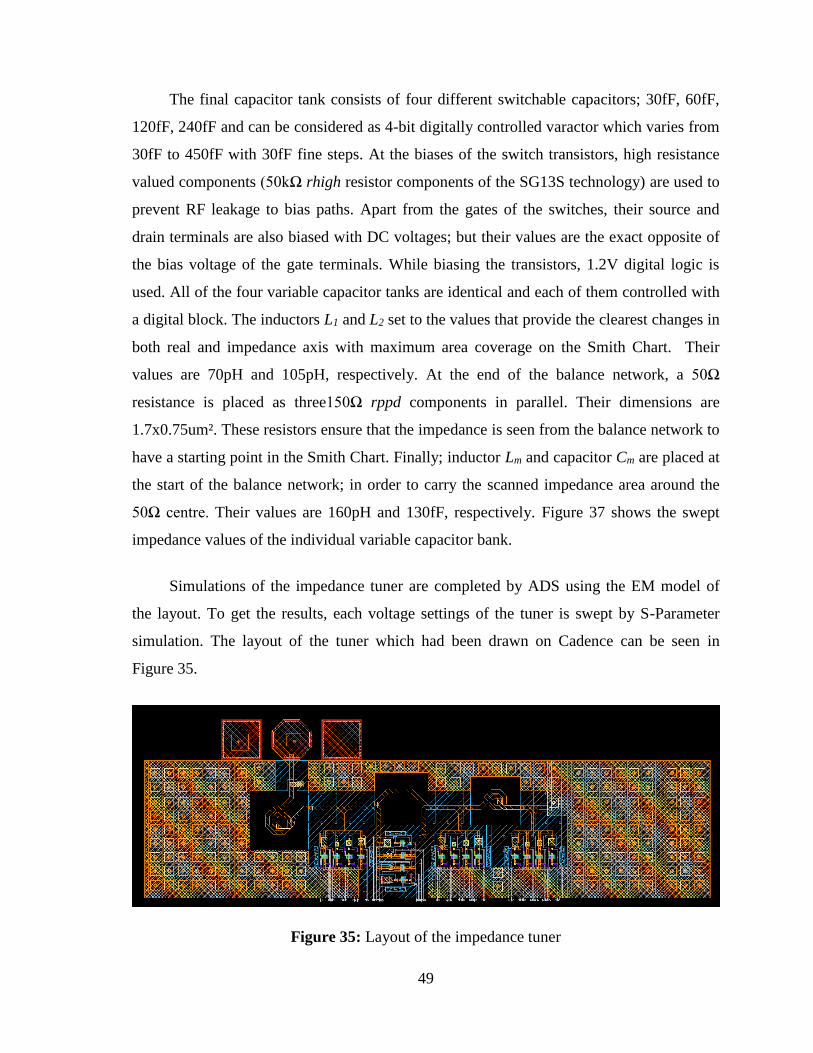
49
The final capacitor tank consists of four different switchable capacitors; 30fF, 60fF,
120fF, 240fF and can be considered as 4-bit digitally controlled varactor which varies from
30fF to 450fF with 30fF fine steps. At the biases of the switch transistors, high resistance
valued components (50kΩ rhigh resistor components of the SG13S technology) are used to
prevent RF leakage to bias paths. Apart from the gates of the switches, their source and
drain terminals are also biased with DC voltages; but their values are the exact opposite of
the bias voltage of the gate terminals. While biasing the transistors, 1.2V digital logic is
used. All of the four variable capacitor tanks are identical and each of them controlled with
a digital block. The inductors L1 and L2 set to the values that provide the clearest changes in
both real and impedance axis with maximum area coverage on the Smith Chart. Their
values are 70pH and 105pH, respectively. At the end of the balance network, a 50Ω
resistance is placed as three150Ω rppd components in parallel. Their dimensions are
1.7x0.75um². These resistors ensure that the impedance is seen from the balance network to
have a starting point in the Smith Chart. Finally; inductor Lm and capacitor Cm are placed at
the start of the balance network; in order to carry the scanned impedance area around the
50Ω centre. Their values are 160pH and 130fF, respectively. Figure 37 shows the swept
impedance values of the individual variable capacitor bank.
Simulations of the impedance tuner are completed by ADS using the EM model of
the layout. To get the results, each voltage settings of the tuner is swept by S-Parameter
simulation. The layout of the tuner which had been drawn on Cadence can be seen in
Figure 35.
Figure 35: Layout of the impedance tuner
50
3.2.2.2 Digital Block
When fully implemented, this impedance tuner block requires 4-bit control from four
identical capacitor banks. In order to deal with all of the switches, using sixteen different
DC bias paths is bulky and costly. That would increase the area of measurement prototype;
because it would require sixteen different pads just for these DC biases. Also, in system
integration sense; routing sixteen DC bias path will be both inefficient and area consuming.
Therefore; to able to control the impedance tuner a digital serial to parallel interface (SPI)
block had been designed. In SPI standards, generally one input is taken each clock cycle,
however; for this case, supplying 16-bit data will take sixteen clock cycles which is quite
long. The longer time required for creating an impedance setting would increase the overall
measurement time of this balance network by an ample amount when the total number of
impedance settings is considered -24 ∗ 24 ∗ 24 ∗ 24-. So that instead of taking 1-bit input
per clock cycle, the digital block is designed to work sequentially and to take 4-bit input in
each clock cycle; in other words, in four clock cycles, digital blocks pushes all the valid
data required for an impedance setting. The smaller time required for each measurement
will lead to the larger possible sample size which means more accurate results for the
balancing network.
The digital control block is firstly designed and simulated with Verilog using Xilinx
ISE Design Suite. It works sequentially and works on simple two staged state machine. The
code has four inputs namely; data_In, clk, start, lead and reset. data_In is the 4-bit input
signal which will be supplied every clock cycle, clk is the clock of the code, reset is the flag
that resets the system and finally start is the flag that is supplied by the user to imply that
code should start to work. First, the user should use reset signal to reset the control code.
Then, when the user is ready to supply 4-bit inputs, the start flag should be set to 1. In that
state, a lead flag is raised so that incoming data can be pushed to the output. In four clock
cycles, the code generates the two 16-bit outputs which are data_Out and
data_Out_inverse. The data_Out signal is supplying the gates of the switches and the
data_Out_inverse signal is supplying the voltage to the source and the drain terminals of
the switch transistors.

51
After implementing and simulating the Verilog code, the next step was generating the
netlist of the code to extract the layout. The netlist of the code generated with Synopsis.
Later on, with generated netlist file and the design files (.lef files) of the IHP
Microelectronics the layout of the digital block is generated via Cadence Encounter. Again,
for this block, the standard cells of the SG13S technology had been used. These standard
digital cells work with 1.2V digital logic. The dimensions and the pin locations of the
digital block specified in the Cadence Encounter so that it can directly fit the overall system
layout.
At the final stage of the layout; the electrostatic discharge (ESD) protection is added
to the pads that are connected to the digital block so that ESD won’t damage the already
fragile transistors in the control circuitry. In order to do so, for each of the pads, two diodes
back-to-back are placed. The chip photo of the impedance tuner can be seen in Figure 36.
Figure 36: Chip photo of the impedance tuner
Figure 38 shows the measured and simulated impedance values seen from the input of
the impedance tuner. The simulated graph shows all 216 states of the block. Light blue dots
show each impedance is seen and dark blue circle depicts the VSWR 2 circle. As can be
seen from the simulated values in the Smith Chart, the tuner can provide a large range of
impedance values while providing the high resolution. The measured results show a subset
of the all possible results due to the infeasibility of measuring all different states. Measured
results show a thousand results from the whole set. As can be seen, the measured results
follow the pattern of the simulation side and provide the desired impedances.

52
Figure 37: Simulated impedances swept by an individual variable capacitor bank
Figure 38: Comparison of a) measured and b) simulated impedance values for states of the
balance network

53
Figure 39: Chip photo of the fabricated EBD
Figure 40: Simulated values of TX- to RX-port isolation for each state of the tuner

54
Figure 39 shows the fabricated chip photo of the final duplexer. The balance network
block is integrated with BALUN transformer by connecting it to the hybrid transformer’s
BAL-port. The measured isolation values can be observed at Figure 40. The EBD can
provide higher than 35dB in the whole frequency range with at least 3GHz bandwidth.
3.3 LNA Design
For this thesis, an LNA which will be used at the RX-port of the EBD is designed and
implemented. The expected results for the LNA were while achieving high output power
with low noise figure value and low power dissipation while maintaining the reasonable
gain level. Due to its location on the EBD system (RX-port), the LNA designed as pseudo-
differential configuration. In order to reach the design goals, two-stage common emitter
topology selected and later on two of the same LNA design connected to differential RX-
port reversed by the x-axis. In the design of this LNA, high performance npn13p BJT
transistors of the SG13S technology has been used. Even though common emitter amplifier
topology causes lower gain and lower reverse isolation when compared to its cascode
counterpart, it provides less noise figure and creates the opportunity of reaching high power
levels without dissipating large DC power thanks to its lower collector voltage than cascode
topology necessity due to the transistor breakdown voltages. The schematic of the LNA is
depicted in Figure 41. In this figure, B.C. is the acronym for bias circuit.
The first stage of the LNA was designed to achieve low noise figure while achieving
a certain saturation power value. Because the common emitter topology with 0.13µm SiGe
BiCMOS technology and at the 28GHz frequency can provide 7 – 9dB gain per stage. To
be able to reach 15dBm output power at the end of the second stage, the first stage of the
LNA must achieve around 9 – 10dBm signal power at its collector node. For this operation
20x transistors with 910mV as their base bias voltage is found to be optimum and as
collector voltage, 1.6V is supplied because it is the given breakdown voltage of npn13p
transistor by technology. As the input signal power increases the collector current (IC) will
increase, therefore there will be more current supplied from the base bias (IB). If a resistor
is used as RF open, the increased IB will cause a voltage drop across the base resistor and

55
will decrease the voltage at the base terminal of the transistors. Therefore, the linearity
performance of the circuitry will degrade. Because of this reason, an inductor has been used
to create RF open for the base bias. However, in this case the base node of transistors
become unprotected, due to the almost zero resistance from bias voltage.
To fix this problem, the bias is supplied via a bias network. Also, between the inductor and
the bias network, a 1pF shunt capacitor is used to short any low-frequency leakage to the
ground. With these bias settings, there was 18mA of IC was flowing through the transistors.
Simultaneous power and noise matching had been done at the input of the first stage. At the
start of the first stage, a 2pF capacitance is used as a DC block. The shunt inductor that
goes to the bias circuit also helps to match the imaginary impedance that is seen through
the base. A degenerate inductor had been used at the emitter node so that the real part is
moved to a close position to 50Ω. While doing the matching an inductor series to the base
terminal is avoided to not to increase the noise figure with the help of transistor numbers.
The output of the first stage matched to a different value of 50Ω which relaxes the burden
on the output matching for the ability to provide enough power to the second stage.
The second stage design is aimed to reach as high 1dB output compression point
(OP1dB) as possible while providing reasonable gain. For this stage, 32x transistor is used
with 852mV as their base voltage. 1.6V collector voltage is supplied to the second stage. At
these bias points, 8mA current flows through the collector. The input of the second stage
was matched to the complex conjugate value of the impedance at the second stage’s output
node. The other concerns in the second stage about base bias are also valid for the second
stage. The output of the second stage was matched to 25Ω, to relax the matching condition
at the output. Also, before the bias pads of both first and the second stage multiple
capacitors with different sizes and values are placed as shunt to the ground in order to
create an RF short. These are shorting low-frequency oscillations to the ground and making
the circuitry invulnerable to any outside effects such as bonds, DC probes that come into
contact with the bias pads.

56
Figure 41: Schematic of the LNA design
After the design of two-stage common emitter LNA, to create the differential status
two of the same design placed on top of each other with one of them reversed. However, in
this case, the same problem with the hybrid transformer measurement occurs which is not
being able to measure differential terminals without GSGSG probes. Again, to overcome
this issue, two different BALUN transformers had been placed at the input and the output.
The input BALUN is the same as the one used for the hybrid transformer which transforms
100Ω differential terminal to singular 50Ω. At the output, due to the matched to the 25Ω
impedance state of the circuit, the located transformer designed to transform differential
50Ω to singular 50Ω. This transformer was also previously designed by İlker Kalyoncu.
All of the inductors are designed custom via Sonnet with using the same layer map of
SG13S IC technology. The EM simulations of other lines and the integration of different
57
parts of the circuit are done via ADS Momentum. The important portions of the ground
layers such as the portion that emitter inductors are connected are simulated carefully;
because even though the ground layer contains all of the metal layers and wide, it still
introduces parasitic inductance to the system and this can change the circuit behaviour
drastically. For instance, it could increase the emitter degenerate inductor unintentionally so
that the matching, gain, linearity behaviours can shift. Finally, the layout of the LNA
completed with using Cadence Virtuoso. The chip photograph of the LNA can be seen in
Figure 42.
Apart from the two-port S-parameter measurements that have done to the fabricated
LNA; noise figure (NF) and 1dB compression point (OP1dB) measurements are also
completed Figure 43 and Figure 44 depicts the measurement setups for these
measurements, respectively. For the NF measurement; first, the noise source is calibrated
with the spectrum analyser. Excess Noise Ratio (ENR) of the noise source and cable losses
are introduced to the spectrum analyser. In order to do so the loss of the two cables together
is measured with probes by contacting a through in a calibration kit. Then, that value
divided into two and these values are determined as input and output cable losses.
For OP1dB, a signal is supplied to the circuits at 28GHz via the signal generator and
from the spectrum analyser the output power values are observed. After the measurement,
the input and output cable losses are considered while evaluating the results.

58
Figure 42: Chip photo of fabricated LNA
Figure 43: NF measurement setup for LNA

59
Figure 44: OP1dB measurement setup for LNA and PA
Figure 45: Measured S11 and S22 behavior of the designed LNA
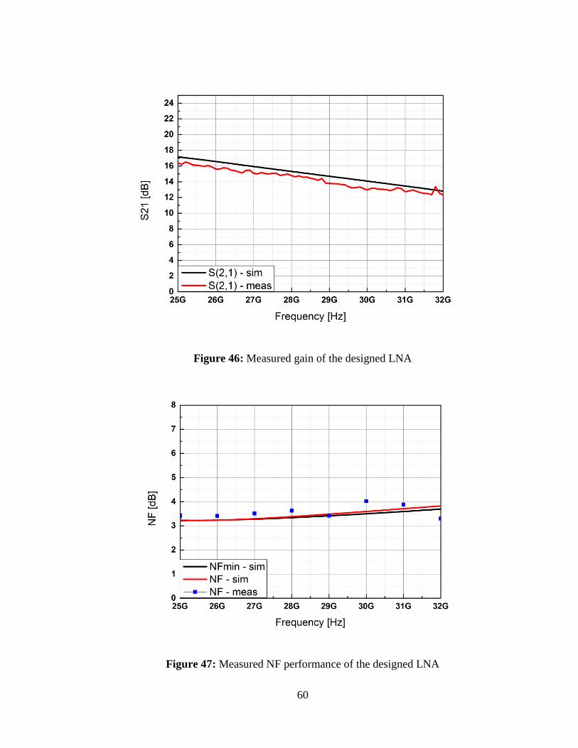
60
Figure 46: Measured gain of the designed LNA
Figure 47: Measured NF performance of the designed LNA

61
Figure 48: Measured 1dB compression point of the designed LNA
Figure 49: Simulated IIP3 value of the LNA w/o input BALUN
62
The measured values for the LNA can be seen in Figure 45-48. Input and output
reflection coefficients are better than -10dB from 25GHz to 32GHz. LNA has 15dB gain at
the center frequency of the 28GHz. While the peak gain is 17dB, lowest gain point in the
frequency band is 13dB. The measured NF value at 28GHz is 3.5dB. Finally, the LNA
compresses at around -2dBm input power while supplying 13.5dBm output power.
Measurement results are following the behavior of the simulations with small errors. It
should be noted that all of these results are including the input and output BALUN
transformer losses. Figure 49 shows the IIP3 performance of the LNA.
3.4 PA Design
For this thesis, a PA that will be connected to TX-port of the EBD had been designed
and implemented. The only design considerations for the PA was high output power with
reasonable gain value. The high performance npn13p BJT transistors are also used for this
design. The PA is also designed as 2 stages; however as different from the LNA, in this
case, the first stage is implemented with the common emitter and the second stage is
implemented with the cascode topologies. The second stage is cascode. Due to the nature of
the EBD, an incoming signal to the antenna splits into RX- and TX-ports. In order to
prevent the signal leakage to the interstage of the PA, the cascode topology becomes
favourable due to its high reverse isolation property even though it increases the overall
power consumption. Furthermore, the DC power dissipation was not a concern of this
design.
The first stage of the design act as a driver amplifier for the second stage. The input,
output matching and biasing concerns are same with the LNA for both first and the second
stage. At the first stage, 24x transistor used with their base bias’s at 900mV and the
collector voltage for this part set to 1.6V. With these bias points the IC of this stage is
18mA. The schematic of the PA can be seen at Figure 50.

63
Figure 50: Schematic of the PA design
The second stage is where the circuits reach to its desired high power. For the second
stage two 48x transistors connected as cascode. For the 48x transistor below; the base point
selected as 920mV. The base biases of the common base transistors are supplied with 2.2V
and finally the collector node is given 3.2V as bias points. With these conditions, IC of this
stage is 59mA. The base of the common base part of the cascode topology comprises an
important point in itself. At that terminal before the base entrance of the transistor, there
must be shunt capacitor that can create an RF short state -especially in high power
operations- so that the possible leaked signal from the collector node to the base can be
shorted. Otherwise, it will create a strong oscillation in the circuit. When the parasitic
inductance seen from the ground layers meets with this capacitor, the self-resonance
frequency of the capacitor can be greatly decreased or even the capacitor can enter in a
series resonance state with this parasitic effect in the desired frequency range and create an
RF open so that, the value of this shunt capacitor can’t be picked as an arbitrary large
capacitance value and must be carefully dealt with. In order to overcome this problem,
whole ground layer that will be seen by this capacitance simulated and the capacitor
selected with an optimal value that can create the RF short. For this case a 350fF shunt
capacitor had been used.
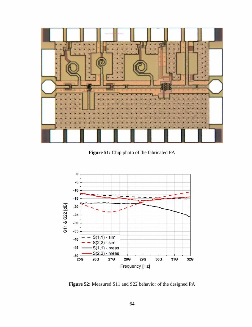
64
Figure 51: Chip photo of the fabricated PA
Figure 52: Measured S11 and S22 behavior of the designed PA
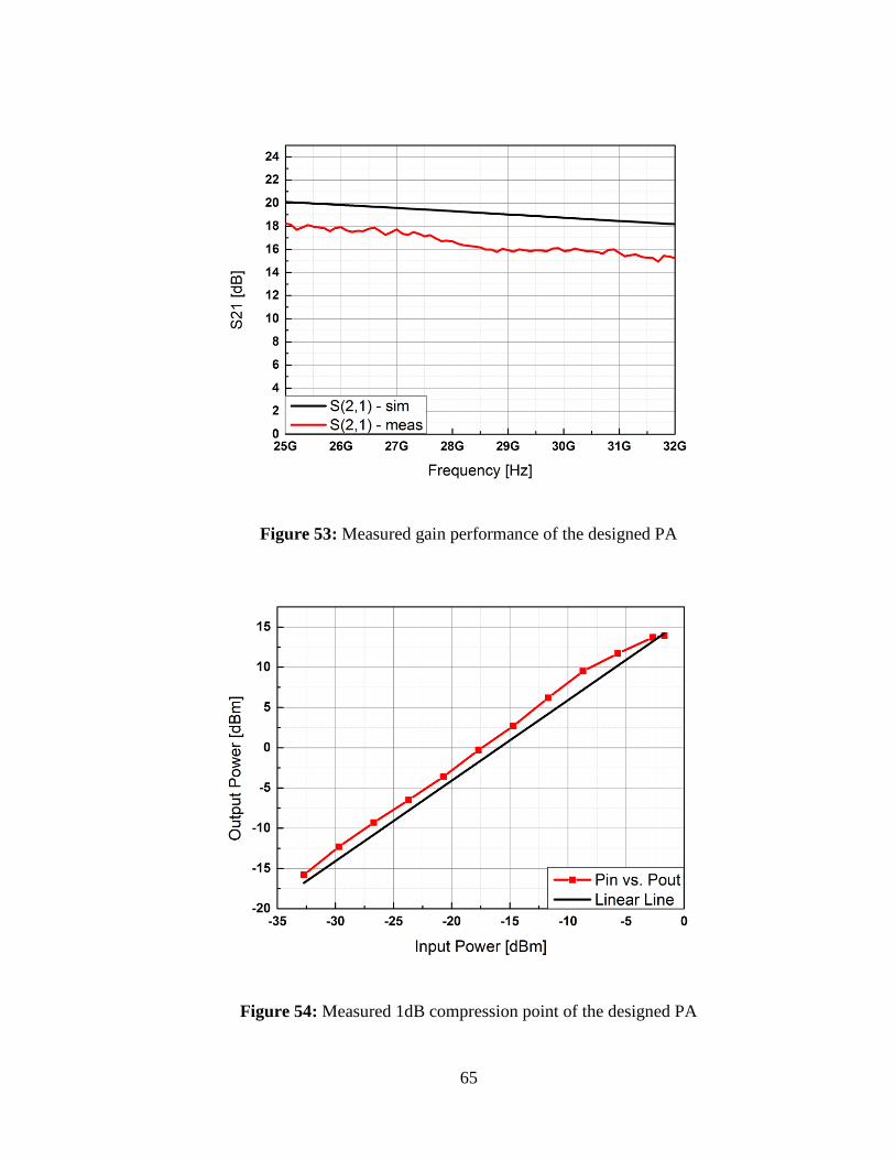
65
Figure 53: Measured gain performance of the designed PA
Figure 54: Measured 1dB compression point of the designed PA
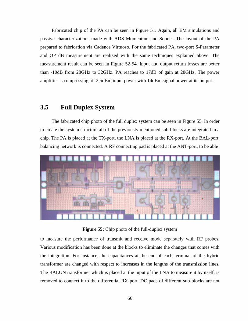
66
Fabricated chip of the PA can be seen in Figure 51. Again, all EM simulations and
passive characterizations made with ADS Momentum and Sonnet. The layout of the PA
prepared to fabrication via Cadence Virtuoso. For the fabricated PA, two-port S-Parameter
and OP1dB measurement are realized with the same techniques explained above. The
measurement result can be seen in Figure 52-54. Input and output return losses are better
than -10dB from 28GHz to 32GHz. PA reaches to 17dB of gain at 28GHz. The power
amplifier is compressing at -2.5dBm input power with 14dBm signal power at its output.
3.5 Full Duplex System
The fabricated chip photo of the full duplex system can be seen in Figure 55. In order
to create the system structure all of the previously mentioned sub-blocks are integrated in a
chip. The PA is placed at the TX-port, the LNA is placed at the RX-port. At the BAL-port,
balancing network is connected. A RF connecting pad is placed at the ANT-port, to be able
Figure 55: Chip photo of the full-duplex system
to measure the performance of transmit and receive mode separately with RF probes.
Various modification has been done at the blocks to eliminate the changes that comes with
the integration. For instance, the capacitances at the end of each terminal of the hybrid
transformer are changed with respect to increases in the lengths of the transmission lines.
The BALUN transformer which is placed at the input of the LNA to measure it by itself, is
removed to connect it to the differential RX-port. DC pads of different sub-blocks are not

67
merged to follow the DC current values of each block separately and clearly and see if they
are matching to their simulation values.
In order to measure the system, the chip was sent to a professional bonding company.
From there, the chip is received as bonded to a QFP208 package. Later, that package was
soldered to PCB board which is designed to supply DC voltages properly. With setup, S-
parameter, OP1dB point and noise figure measurements were conducted for TX- to ANT
path and ANT- to RX path, separately. For each measurement, previously mentioned
techniques have been used.
The measurement results for the PA that is placed at the TX-ANT path can be seen at
Figure 56-58. Both input and output return losses of this path is better than -10dB in the
whole frequency band. A small oscillation behaviour can be observed around 29GHz, due
to the RF cables and probes that had been used during the measurement. Figure 55 shows
the gain of the amplifier is 14.7dB at 28GHz. Even though expected gain drop from the
individual measurement (Figure 51) is 3.8dB (Figure 27), there is only 2dB loss that was
caused by the hybrid transformer.
Figure 56: Measured input and output reflection coefficients of TX-ANT path

68
Figure 57: Measured gain of TX-ANT path
Figure 58: Output power graph of TX-ANT path with respect to input power

69
Reasoning for this behaviour is the badly matched balance network. During
measurements, the impedance of the balance network couldn’t be matched to the perfect
value so that there is an impedance difference between ANT- and BAL-port. This will
cause the output signal of the PA to not to divide equally. In this case, higher portion of the
signal is flowing to the ANT-port. Figure 58 shows the OP1dB of TX-ANT path. The
output compression point dropped by 3dB when compared to PA’s individual measurement
(Figure 54). It is 1dB higher than the gain loss.
The rest part of the circuit meant to be measured however due to bonding of the chip
part of the transistors in the circuit is broken. Simulated performance of the ANT-RX path
can be seen from Figure 59-62. For these results, post-layout simulation results of the
hybrid transformer at its highest isolation setting and post-layout simulation results of the
LNA without its input BALUN transformer. Even though, these graphs don’t represent real
measurements, they can give hints about the performance. The calculated results that have
been gathered in the light of measured results can be seen at Table 2.
Figure 59: Simulated input and output return losses of the ANT-RX path

70
Figure 60: Simulated gain performance of the ANT-RX path
Figure 61: Simulated NF behavior of the ANT-RX path

71
Figure 62: Simulated 1dB compression point performance of the ANT-RX path
In the simulations both the ANT-port and the output of the LNA have return losses
better than 10dB in whole frequency range. The gain has been dropped by around 4.8dB
which is in line with the RX insertion loss of hybrid transformer (Figure 27). The NF of the
system is first decreased with absence of the input BALUN transformer but increased with
the loss from the hybrid transformer and reached to 6.8dB at 28GHz. Also, in the
simulations, LNA reaches to 12dBm OP1dB.
3.6 Comparison
Table 2 shows the comparison of this thesis work with other reported designed. This
study is one of the few works on EBD concept which operates higher than 2.5GHz. The
frequency spec is creating the biggest challenge on hybrid transformer and balance network
design. Also, this work is representing the results of a system which includes not only
hybrid transformer and balance network, but LNA and PA as well. When compared to
other works, the EBD occupies much less area with frequency component is considered.
Even though isolation from TX- to RX-port is relatively small, it has the highest isolation
bandwidth of all.

72
Tab
le 2
: C
om
par
ison 5
G f
ull
-duple
x s
yst
em w
ith o
ther
rep
ort
ed w
ork
s
Tec
hn
olo
gy
0.1
8 µ
m
SO
I
CM
OS
0.1
8µ
m
CM
OS
0.1
8µ
m
SO
I
CM
OS
0.1
8µ
m
CM
OS
40
nm
CM
OS
0.2
5µ
m
SiG
e
BiC
MO
S
0.1
3µ
m
SiG
e
BiC
MO
S
* A
ssu
med
fro
m t
he
chip
ph
oto
⸆ P
ost
-lay
ou
t E
M s
imu
lati
on
res
ult
⸆⸆ C
alc
ula
ted
wit
h k
no
wn
res
ult
s
Co
ver
ag
e
ZA
NT
[VS
WR
]
< 2
.3:1
<1
.3:1
<1
.5:1
X
X
X
<1
.5:1
Du
ple
xer
Are
a
[mm
²]
0.7
92*
0.3
45*
0.2
75*
0.6
7
0.0
15*
0.0
62*
0.0
3
RX
Po
wer
[dB
m]
X
X
X
X
X
X
9⸆⸆
RX
NF
[dB
]
9
6.5
X
X
X
4
6.7⸆⸆
RX
Ga
in-
Lo
ss
[dB
]
5
X
X –
3.9
X -
11
X -
12
18
- X
10
.8⸆⸆
– 4
.8⸆
TX
Po
wer
[dB
m]
29
.2
22
27
x
X
X
11
TX
Ga
in-
Lo
ss
[dB
]
X –
3.8
X -
3.2
X –
3.7
X –
3
X -
11
X -
3.1
14
.7–
3.8⸆
Iso
lati
on
Ba
nd
wid
th
[MH
z]
3.2
40
0
30
0
20
14
00
0
20
00
30
00
Iso
lati
on
[dB
]
40
40
50
50
30
40
35
Iso
lati
on
Tec
hn
iqu
e
EB
D
EB
D
EB
D
EB
D
EB
D
EB
D
EB
D
Fre
qu
ency
[GH
z]
0.7
- 1
.0
1.6
- 2
.2
1.9
– 2
.2
1.7
5 –
2
12
0
27
- 3
2
25
- 3
2
Wo
rk
[12
]
[19
]
[20
]
[14
]
[21
]
[22
]
Th
is
Wo
rk

73
4 Conclusion & Future Work
4.1 Summary of the Work
The next generation communication systems require high data rate, wider bandwidth,
high spectral efficiency, and lower latency to meet the demands of users as number of
devices/users and data requirement increase. Therefore, technology is moving forward to
systems that operates at higher frequencies to increase the bandwidth so that newly
designed transceiver circuits have been started to design with such centre frequencies. The
other requirements such as spectral efficiency and latency, full-duplex structures can offer a
solution; because, these types of systems allow transceiver blocks to operate at transmit and
receive modes concurrently while using same frequencies in their designs. The recent
progresses in the SiGe BiCMOS technology makes this process suitable for this type of
applications not just with their high fT and fmax and cheaper fabrication cost with respect to
other common processes as well.
In this thesis, a Ka-band (25GHz – 32GHz) full-duplex system for 5G applications is
presented. Each block of this system is fabricated, analysed and measured separately.
These blocks are a hybrid transformer, a balancing network, an LNA and a PA. In order to
provide full-duplex operation, a four ports hybrid transformer with balancing network is
used as duplexer between transmitter, receiver, and antenna ports. The hybrid transformer
has 1:2 turn ratio, to create desired impedances at each of its terminals and to acquire less
area. The balancing network is designed to provide high impedance range without large
gaps between each impedance value. It is designed with switched capacitor technique and
for switches isolated NMOS transistors have been used. To efficiently sweep the states of
this tuner with lesser DC pads, a digital block is designed and synthesized. For LNA, two
common emitter amplifiers are cascaded and later connected to the differential ports of
receiver port of the hybrid transformer. Common emitter topology has been selected to
decrease the power consumption even though it would lead to less gain. First stage is
designed to get lower noise figure while second stage was aimed to reach high output
compression point. For PA a common emitter topology is selected for the first stage and
cascode topology for the second. Cascode topology is used to because of its high reverse

74
isolation property that can prevent the signal coming from the antenna to leak to the
entrance of the PA. In chapter 3, the design steps and measurement results are explained
and discussed. Finally, the full-duplex system which includes the hybrid transformer, the
balancing network, the PA and the LNA; is integrated and the measurement results are
represented.
4.2 Future Work
The first short-term future work for this study is more detailed measurements of the
system to fully understand the positive and negative sides of the design clearly to
compensate these flaws or boost the plusses in later batches. The second short-term future
work for this study is further optimization of the EBD through more detailed
characterization with other simulation tools. Isolation walls between the blocks of the
system can be placed in order to block the signal that leaks to the substrate. These isolation
walls can be created by via stacks from the highest metal of the technology to the substrate.
Apart from the characterization, the placement of the blocks can be altered to acquire less
area than before.
As a long-term future work, this system can be modified to be suitable for flip-chip
bonding. With such a high frequency like 28GHz it is hard to propagate the input or output
RF signals to a board. Flip-chip bonding is one of the most popular bonding methods for
circuits that operate at high frequencies. So that the integration capability of the circuitry to
a larger scale system can be furtherly increased.

75
5 References
[1] P. Rost, V. Jungnicke, and 5G PPP Architecture Working Group, “View on 5G
Architecture,” 5G PPP White Pap., no. July, p. 61, 2016.
[2] Cisco, “Cisco Visual Networking Index: Global Mobile Data Traffic Forecast
Update, 2011–2016 [Visual Networking Index (VNI)],” Cisco, pp. 2016–
2021, 2012.
[3] A. M. Niknejad, S. Thyagarajan, E. Alon, Y. Wang, and C. Hull, “A Circuit
Designer ’ s Guide to 5G mm-Wave,” 2015.
[4] J. G. Andrews, S. Buzzi, W. Choi, S. V Hanly, A. Lozano, A. C. K. Soong, and J. C.
Zhang, “What will 5G be?,” arXiv Prepr. arXiv1405.2957, vol. 32, no. 6, pp.
1065–1082, 2014.
[5] F. Boccardi, R. Heath, A. Lozano, T. L. Marzetta, and P. Popovski, “Five disruptive
technology directions for 5G,” IEEE Commun. Mag., vol. 52, no. 2, pp. 74–80, 2014.
[6] Z. Zhang, X. Chai, K. Long, A. V Vasilakos, and L. Hanzo, “Full Duplex
Techniques for 5G Networks : Protocol Design , and Relay Selection,” IEEE
Commun. Mag., no. May, pp. 2–10, 2015.
[7] A. Tessmann, S. Kudszus, T. Feltgen, M. Riessle, C. Sklarczyk, and W. H. Haydl,
“Compact single-chip W-band FMCW radar modules for commercial high-
resolution sensor applications,” IEEE Trans. Microw. Theory Tech., vol. 50, no. 12,
pp. 2995–3001, 2002.
[8] D. J. Huang, J. L. Kuo, and H. Wang, “A 24-GHz low power and high isolation
active quasi-circulator,” IEEE MTT-S Int. Microw. Symp. Dig., no. Path 3, pp. 31–
33, 2012.
[9] “Series OMT | Orthomode Transducers.” [Online]. Available:
http://www.millitech.com/MMW-Antenna-OrthomodeTransducer.htm. [Accessed:
17-Jul-2018].
[10] H. Dong, T. X. Wu, K. S. Cheema, B. P. Abbott, C. A. Finch, and H. Foo, “Design

76
of miniaturized RF SAW duplexer package,” IEEE Trans. Ultrason. Ferroelectr.
Freq. Control, vol. 51, no. 7, pp. 849–858, 2004.
[11] B. Van Liempd, B. Hershberg, K. Raczkowski, S. Ariumi, U. Karthaus, K. F. Bink,
and J. Craninckx, “A +70dBm IIP3 single-ended electrical-balance duplexer in
0.18um SOI CMOS,” Dig. Tech. Pap. - IEEE Int. Solid-State Circuits Conf., vol. 58,
pp. 32–33, 2015.
[12] G. Qi, B. Van Liempd, P. I. Mak, R. P. Martins, and J. Craninckx, “A SAW-Less
Tunable RF Front End for FDD and IBFD Combining an Electrical-Balance
Duplexer and a Switched-LC N-Path LNA,” IEEE J. Solid-State Circuits, vol. 53,
no. 5, pp. 1431–1442, 2018.
[13] S. H. Abdelhalem, P. S. Gudem, and L. E. Larson, “Tunable CMOS integrated
duplexer with antenna impedance tracking and high isolation in the transmit and
receive bands,” IEEE Trans. Microw. Theory Tech., vol. 62, no. 9, pp. 2092–2104,
2014.
[14] B. Van Liempd, “A Dual-Notch + 27dBm Tx-Power Electrical-Balance Duplexer,”
pp. 463–466.
[15] K. R. Boyle, Y. Yuan, and L. P. Ligthart, “Analysis of mobile phone antenna
impedance variations with user proximity,” IEEE Trans. Antennas Propag., vol. 55,
no. 2, pp. 364–372, 2007.
[16] J. R. Long, “Monolithic transformers for silicon RF IC design,” IEEE J. Solid-State
Circuits, vol. 35, no. 9, pp. 1368–1382, 2000.
[17] E. F. Sartori, “Hybrid Transformers,” IEEE Trans. Parts, Mater. Packag., vol. 4, no.
3, pp. 59–66, 1968.
[18] M. Mikhemar, H. Darabi, and A. A. Abidi, “A multiband RF antenna duplexer on
CMOS: Design and performance,” IEEE J. Solid-State Circuits, vol. 48, no. 9, pp.
2067–2077, 2013.
[19] M. Elkholy, M. Mikhemar, H. Darabi, and K. Entesari, “Low-Loss Integrated
Passive CMOS Electrical Balance Duplexers With Single-Ended LNA,” IEEE

77
Trans. Microw. Theory Tech., vol. 64, no. 5, pp. 1544–1559, 2016.
[20] B. Van Liempd, B. Hershberg, S. Ariumi, K. Raczkowski, K. F. Bink, U. Karthaus,
E. Martens, P. Wambacq, and J. Craninckx, “A +70-dBm IIP3 Electrical-Balance
Duplexer for Highly Integrated Tunable Front-Ends,” IEEE Trans. Microw. Theory
Tech., vol. 64, no. 12, pp. 4274–4286, 2016.
[21] N. Van Thienen and P. Reynaert, “A 120GHz in-band full-duplex PMF transceiver
with tunable electrical-balance duplexer in 40nm CMOS,” ESSCIRC 2017 - 43rd
IEEE Eur. Solid State Circuits Conf., no. 1, pp. 103–106, 2017.
[22] C. Lu, M. K. Matters-Kammerer, A. Zamanifekri, A. B. Smolders, and P. G. M.
Baltus, “A Millimeter-Wave Tunable Hybrid-Transformer-Based Circular
Polarization Duplexer with Sequentially-Rotated Antennas,” IEEE Trans. Microw.
Theory Tech., vol. 64, no. 1, pp. 166–177, 2016.
[23] J.D. Cressler, Fabrication of SiGe HBT BiCMOS Technology. Florida: CRC Pres,
aaaaaaıTaylor & Francis Group, 2005
[24] B. Ustundag, “0.13 µm SiGe BiCMOS W&D-BAND Receivers for Passive
aaaaaaiMillimeter-Wave Imaging Applications”, (Master Dissertation), Sabanci
aaaaaaUniversity, i2016


![Duplex and Super Duplex [Fittings and Flanges] final](https://img.pdfslide.us/doc/110x75/61a6ddf752ba2a16af77519c/duplex-and-super-duplex-fittings-and-flanges-final.jpg)