Embed Size (px)
Citation preview

MAINTENANCE MANUAL
KA 57AUTOPILOT ADAPTER
MANUAL NUMBER 006-15629-0007REVISION 7 DECEMBER, 2001

WARNINGPrior to the export of this document, review for export license requirement is needed.
COPYRIGHT NOTICE
©1975-2001 Honeywell International Inc.
Reproduction of this publication or any portion thereof by any means without the express written permission of Honeywell is prohibited. For further information contact the manager, Technical Publications, Honeywell, One Technology Center, 23500 West 105th Street Olathe KS 66061 telephone: (913) 712-0400.

BENDIX/KING KA 57
Rev 7, Dec/2001 15629M07.JA Page RH-1
REVISION HISTORY
KA 57 Maintenance Manual
Part Number: 006-15629-XXXX
For each revision, add, delete, or replace pages as indicated.
REVISION No. 7, December 2001
Revision 7 creates a new stand-alone manual for the KA 57 which was extracted from revision 6 of the KCS 55/55A maintenance manual, (P/N 006-05111-0006). Any revisions to the KA 57, be-ginning with revision 7, will not be a part of the KCS 55/55A manual.
ITEM ACTION
All pages Full Reprint, new manual

BENDIX/KING KA 57
Page RH-2 15629M07.JA Rev 7, Dec/2001
THIS PAGE IS RESERVED

BENDIX/KING KA 57
Rev 7, Dec/2001 15629M07.JA Page i
TABLE OF CONTENTS
SECTION IVTHEORY OF OPERATION
PARAGRAPH PAGE
4.1 General 4-1
4.2 Input Buffer 4-1
4.3 Modulator 4-1
4.4 Logic Section 4-1
4.5 Output Stage 4-2
4.6 Nav-O-Matic Operation 4-2
SECTION VMAINTENANCE
PARAGRAPH PAGE
5.1 General Information 5-1
5.2 Purpose 5-1
5.2.1 General Requirements 5-1
5.2.2 Test Requirements 5-2
5.3 Overhaul 5-5
5.3.1 Visual Inspection 5-5
5.3.2 Cleaning 5-6
5.3.3 Repair 5-11
5.3.4 Disassembly/Assembly Procedures 5-15
5.4 Troubleshooting 5-15
SECTION VIILLUSTRATED PARTS LIST
PARAGRAPH PAGE
6.1 General 6-1
6.2 Revision Service 6-1
6.3 List of Abbreviations 6-1
6.4 Sample Parts List 6-3
6.5 KA 57 Final Assembly 6-5
6.6 KA 57 Autopilot Adapter Board 6-11

BENDIX/KING KA 57
Page ii 15629M07.JA Rev 7, Dec/2001
LIST OF ILLUSTRATIONS
FIGURE PAGE
5-1 KA 57 Test Set Schematic 5-4
5-2 KA 52 Troubleshooting Flow Chart 5-16
6-1 Sample Parts List 6-3
6-2 KA 57 Final Assembly 6-7
6-3 KA 57 P.C. Board Assembly 6-13
6-4 KA 57 P.C. Board Schematic 6-17

BENDIX/KING KA 57
Rev 7, Dec/2001 15629M07.JA Page 4-1
SECTION IVTHEORY OF OPERATION
4.1 GENERALThe KA 57 Autopilot Adapter interfaces the DC course and heading output signals of the KI 525 PNI to autopilots that require AC course and heading inputs. The KA 57 has four basic sections: an input buffer for a high impedance input; a modulator which converts the DC input signal into an AC signal; a logic section which selects the proper input signal and output phase; and an output stage which fixes the output amplitude and also provides a tracer signal for logic switching. Each of these sections is described below. Refer to KA 57 schematic, Figure 6-4.
4.2 INPUT BUFFERThe input to the KA 57 is through a parallel combination of two FET analog switches I106A and B) connected to the inverting input of a differential amplifier (I101A pin 2). The differential amplifier provides a high impedance isolating input while the logic circuitry selects either the course or heading signal for the amplifier input by placing a ground potential on the gate of the appropriate FET switch.
4.3 MODULATORThe modulator converts the DC output of the input buffer into an AC signal to drive the output stage. The active components of the modulator are Q107 which is driven by a 5KHz square wave from the logic section, and FET Q101 which is switched between full on and pinch off by the signal from the collector of Q107. As Q101 switches from full off to full on it alternately presents a high impedance and then ground to the junction of R105 and C106. This produces a square wave at this junction alternating at a 5KHz rate between ground and the buffer output voltage level. The two capacitors C106 and C107 remove the DC component of the square wave so the input to the output stage is a square wave centered around zero volts whose peak-to-peak amplitude is equal to the DC voltage of the buffer output.
4.4 LOGIC SECTIONThe logic section selects the proper buffer input signal and output loop gain by monitoring the Ra-dio Coupler output for the presence of the tracer signal. Similarly from the high (open) or low (ground) state of the LOCALIZER ENERGIZED and LOCALIZER. NORMAL lines the logic section determines the proper phase for the output signal.The presence of the tracer signal on the radio coupler output is detected by the high pass active filter and envelope detector formed by I104 and its associated parts and the diode and resistor-capacitor combination of CR101, R116 and C105. When the tracer signal is present in sufficient amplitude, it passes through the filter and the detector converts it into a DC signal keeping Q106 in the ON state. The resulting low state at the collector of Q106 is passed through I103 and is seen as a low at the gates of I106A and I107A. A low signal at these gates connects the heading signal into the buffer amplifier (I101A) and closes the loop around the output stage amplifier (I101B) with R108 setting the loop gain.The logic section determines the KA 57 output phase by using the 5KHz reference signal and the high or low state of the LOCALIZER ENERGIZED and LOCALIZER NORMAL lines. The output signal phase is referenced to the REF AC MODULATOR DRIVE which is coupled into the logic circuit by transformer T101.

BENDIX/KING KA 57
Page 4-2 15629M07.JA Rev 7, Dec/2001
This signal is reduced in amplitude by the voltage divider R122 and R123, clipped by CR102, and applied to one side of a two input "exclusive or" logic circuit (pins 5 and 8 of I102).It is the characteristic of an "exclusive or" circuit that the output is high only when just one of the inputs is high. For any other condition, two low inputs, two high inputs, the "exclusive or" output is low. In the logic section by controlling the second input to the "exclusive or", the output can be made to switch in phase with the applied reference signal or 180 deg. out of phase with the refer-ence signal.For example, when the second input to the "exclusive or’ circuit is low the output will be high when the reference square wave is high, and low when the reference signal is low. However, when the second input to the circuit is high and the reference input is high the output is low and when the reference input is low the output is high. In this way, the "exclusive or" output is in or out of phase with the reference input according to the state of the second "exclusive or" input.The second input to the "exclusive or" circuit is the logical AND of the LOC ENG, LOC NORMAL, and course position of the Radio Coupler selector switch. When the LOC ENG line is low (ground) and the LOC NORMAL line is high (open) and the coupler selector switch is in the LOC REV po-sition the second input to the "exclusive or" circuit (I102 pins 1 and 2) will be high and the "exclu-sive or" circuit output (I102 pin 11) will be the reverse of the reference signal input.The output of the "exclusive or" circuit is applied to the base of Q107 which in turn drives the FET modulator Q101 which produces the square wave drive for the output stage.
4.5 OUTPUT STAGEThe output stage consists of a variable gain amplifier connected to a complementary emitter fol-lower pair which drives the output transformer, and an oscillator coupled to the secondary of the output transformer which produces the tracer signal for the heading logic.The input to the variable gain amplifier (I101B) is the 5KHz square wave from the modulator sec-tion. This signal is amplified by a factor determined by the setting of one of the two variable resis-tors in the feedback loop (R108 or R109). Which of the two variable resistors will be connected in the feedback loop is determined by the logic circuitry which places a ground on the gate of the appropriate FET switch (I107A for Heading, I107B for Course). The emitter follower complimenta-ry pair Q102, Q103 drives the output transformer.Amplifier 1105 forms the tracer oscillator and is coupled to the output circuit through C110. The oscillator frequency is determined by RC components R112 and C108. Hysteresis adjustment is performed with R132 which is used to adjust the oscillator output amplitude during system calibra-tion.
4.6 NAV-0-MATIC OPERATIONThe following is a brief description of the operation of the KA 57 when it is the interface between the KCS 55 and the NAV-0-MATIC 400.The KA 57 wired for operation with the Nav-0-Matic 400 Autopilot has a jumper wire connecting J101 pin 1 to pin D of the KA 57. The jumper connects the base of Q106 to +5VDC through R131 and causes Q106 to conduct. The resulting low state of the collector of Q106 reflected through the logic of 1103 places a ground at the gates of the FET analog switched I106A and I107A closing the switches. This connects the Heading input into the Buffer amplifier I101A and sets the gain of the Output stage by closing the loop around I101B and R108. The Course input switches into the KA 57 when J101 pin C is switched to ground through the INTERCEPT -TRK-HDG switch of the Nav-O-Matic 400 Controller box. A ground on pin C reduces the base voltage of Q106 below the turn on level and Q106 stops conduction.

BENDIX/KING KA 57
Rev 7, Dec/2001 15629M07.JA Page 4-3
The collector potential of Q106 rises to +10VDC which when reflected through the logic of I103 places a ground at the gates of the FET analog switches I106B and I107B. This closes the switch and connects the Course input into the buffer amplifier and sets the gain of the output stage by closing the loop around I101B with R109.The Tracer-Oscillator (I105) and the logic switching section Q105, Q104) of the KA 57 are not used with the Nav-O-Matic 400 Autopilot system and may be disabled by removing CJ101.A similar interface situation occurs with the Mitchell Century IC388 Radio Couplers above serial number 6000. In this system, the tracer oscillator and the sense amplifier I104 are deactivated. Pin A of J101 is grounded and a jumper is connected between J101 pins D and 1. Oscillator I105 is deactivated by adjusting the wiper of R132 at the ground side of the potentiometer. A control switch is connected to pin J101-C such that an OPEN appears at pin C during Heading Operation and a GROUND appears during NAV operation. On Mitchell Century systems with radio couplers IC388, IC388M and IC388P, an additional circuit consisting of C116, L101, and R133 is provided to supply the proper DG excitation load to the system.

BENDIX/KING KA 57
Page 4-4 15629M07.JA Rev 7, Dec/2001
THIS PAGE IS RESERVED

BENDIX/KING KA 57
Rev 7, Dec/2001 15629M07.JA Page 5-1
SECTION VMAINTENANCE
5.1 GENERAL INFORMATIONThis section covers the testing, overhaul, and troubleshooting procedures for the KA 57 Autopilot adapter.
5.2 PURPOSEThe following establishes the performance requirements that this unit must meet before it can be used as part of an operational system.
5.2.1 General Requirements
Unless otherwise specified, all test shall be conducted with the unit in its normal position, at normal room temperature (25 deg. ±5 deg. C), and at a relative humidity less than 80%.
Electrical Output Signalsa. HDG/CRS SIG: either the Heading or Course Datum signal as determined by the
radio coupler selector switch.Electrical Input Signalsa. HEADING ERROR: a dc input from the KI 525 scaled at 0.6v/deg with positive volt-
ages representing increasing heading commands.b. COURSE DATUM ERROR: a dc input from the KI 525 scaled at 0.3v/deg with pos-
itive voltages representing increasing course commands.c. REF AC MODULATOR DRIVE: a 5KHz square wave from the aircraft autopilot
system.d. LOC NORMAL: a ground at this input indicates that the radio coupler is in the LOC
normal mode.e. LOC ENERGIZE: a ground at this point indicates that the radio is turned to a local-
izer frequency.Power Inputa. +15v at 30mAb. -15v at 10mASignal Test Sources and Test Equipmenta. Electronic test circuitry as shown in Figure 5-1b. Test Equipment
DC Voltmeter: Hewlett Packard model 412A or equivalent.AC Voltmeter: Ballantine Lab, Inc. model 300G or equivalent.Oscilloscope: Tektronix model 516 or equivalent.

BENDIX/KING KA 57
Page 5-2 15629M07.JA Rev 7, Dec/2001
5.2.2 Test Requirements
Remove the cover from the KA 57 and connect the unit to the Test Set as shown in Figure 5-1.Set the following switches and potentiometers as noted:
KA 57 CRS pot Midway between end stops.HDG pot. Midway between end stops.TEST SET LOC NOR OPEN
LOC ENG OPENINPUT FULL CCWHDG/CRS HDG
Turn on the power to the test set and measure the following voltages:+15v ±0.4v at pin 5 referred to pin F-15v ±0.4v at pin K referred to pin F10v ±2vpp at 5KHz ±500Hz between pins 4 and E
Function CheckSet the following switches as indicated:
LOC NOR OPENLOC ENG OPENHDG/CRS HDGNAV JUMPER OPENNAV SIG OPENa) With the oscilloscope vertical calibration set at 5v/cm observe the waveform at pin
2. Slowly vary the INPUT potentiometer from full CCW to full CW. The voltage at pin 2 should remain at +0.7v ±0.3v through the full range of the potentiometer.
b) Using the INPUT potentiometer set the voltage at pin 10 to 0.0v ±0.20vdc. The volt-age at pin 2 should be 0.7v ±0.3v.
c) With the voltage at pin 10 set as in step b above, observe the voltage at pin 2. Change the HDG /CRS switch to CRS. The voltage at pin 2 should go from 0.7v to 5.0v ±0.25v.
d) Observe the voltage at pin 2 with the oscilloscope and vary the input potentiometer from full CCW to full CW. The voltage at pin 2 should remain at 5.0v ±0.25v.
e) Switch the NAV JUMPER switch closed. The voltage at pin 2 should be 0.7v ±0.3v.f) Switch the NAV SIG switch closed. The voltage at pin 2 should be 5.0 ±0.25v. Re-
turn NAV JUMPER and NAV SIG to OPEN.Phase Check
a) Set the following switches as indicated.LOC ENG CLOSEDLOC REV CLOSEDHDG/CRS CRSNAV JUMPER OPENNAV SIG OPEN
b) Using the External Sync of the oscilloscope trigger the oscilloscope sweep with the positive going edge of the 5KHz Ref Drive available at test point 1 of the test set. With the oscilloscope observe the waveform at pin C. The leading edge of the ob-served signal should be positive going.
BENDIX/KING KA 57
Rev 7, Dec/2001 15629M07.JA Page 5-3
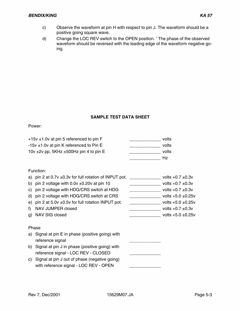
c) Observe the waveform at pin H with respect to pin J. The waveform should be a positive going square wave.
d) Change the LOC REV switch to the OPEN position. ’ The phase of the observed waveform should be reversed with the leading edge of the waveform negative go-ing.
SAMPLE TEST DATA SHEET
Power:
+15v ±1.0v at pin 5 referenced to pin F _____________ volts
-15v ±1.0v at pin K referenced to Pin E _____________ volts
10v ±2v pp, 5KHz ±500Hz pin 4 to pin E _____________ volts
_____________ Hz
Function:
a) pin 2 at 0.7v ±0.3v for full rotation of INPUT pot. _____________ volts +0.7 ±0.3v
b) pin 2 voltage with 0.0v ±0.20v at pin 10 _____________ volts +0.7 ±0.3v
c) pin 2 voltage with HDG/CRS switch at HDG _____________ volts +0.7 ±0.3v
d) pin 2 voltage with HDG/CRS switch at CRS _____________ volts +5.0 ±0.25v
e) pin 2 at 5.0v ±0.5v for full rotation INPUT pot. _____________ volts +5.0 ±0.25v
f) NAV JUMPER closed _____________ volts +0.7 ±0.3v
g) NAV SIG closed _____________ volts +5.0 ±0.25v
Phase
a) Signal at pin E in phase (positive going) with
reference signal _____________
b) Signal at pin J in phase (positive going) with
reference signal - LOC REV - CLOSED _____________
c) Signal at pin J out of phase (negative going)
with reference signal - LOC REV - OPEN _____________

BENDIX/KING KA 57
Page 5-4 15629M07.JA Rev 7, Dec/2001
FIGURE 5-1 KA 57 TEST SET SCHEMATIC
BENDIX/KING KA 57
Rev 7, Dec/2001 15629M07.JA Page 5-5
5.3 OVERHAUL
5.3.1 VISUAL INSPECTION
This section contains instructions and information to assist in determining, by visual inspection, the condition of the units major assemblies and subassemblies. These inspection procedures will assist in finding defects resulting from wear, physical damage, deterioration, or other causes. To aid inspection, detailed procedures are arranged in alphabetical order.
A. Capacitors, FixedInspect capacitors for case damage, body damage, and cracked, broken, or charred insulation. Check for loose, broken, or corroded terminal studs, lugs, or leads. Inspect for loose, broken, or improperly soldered connections. On chip caps, be especially alert for hairline cracks in the body and broken terminations.
B. Capacitors, VariableInspect trimmers for chipped and cracked bodies, damaged dielectrics, and dam-aged contacts.
C. ChassisInspect the chassis for loose or missing mounting hardware, deformation, dents, damaged fasteners, or damaged connectors. In addition, check for corrosion or damage to the finish that should be repaired.
D. Circuit BoardsInspect for loose, broken, or corroded terminal connections; insufficient solder or improper bonding; fungus, mold, or other deposits; and damage such as cracks, burns, or charred traces.
E. ConnectorsInspect the connector bodies for broken parts; check the insulation for cracks, and check the contacts for damage, misalignment, corrosion, or bad plating. Check for broken, loose, or poorly soldered connections to terminals of the connectors. In-spect connector hoods and cable clamps for crimped wires.
F. Covers and ShieldsInspect covers and shields for punctures, deep dents, and badly worn surfaces. Al-so, check for damaged fastener devices, corrosion and damage to finish.
G. Flex CircuitsInspect flex circuits for punctures, and badly worn surfaces. Check for broken trac-es, especially near the solder contact points.
H. Front PanelCheck that name, serial, and any plates or stickers are secure and hardware is tight. Check that the handle is functional, securely fastened, and handle casting is not damaged or bent.
I. FuseInspect for blown fuse and check for loose solder joints.
J. InsulatorsInspect insulators for evidence of damage, such as broken or chipped edges, burned areas, and presence of foreign matter.
K. JacksInspect all jacks for corrosion, rust, deformations, loose or broken parts, cracked insulation, bad contacts, or other irregularities.

BENDIX/KING KA 57
Page 5-6 15629M07.JA Rev 7, Dec/2001
L. PotentiometersInspect all potentiometers for evidence of damage or loose terminals, cracked in-sulation or other irregularities.
M. Resistors, FixedInspect the fixed resistors for cracked, broken, blistered, or charred bodies and loose, broken, or improperly soldered connections. On chip resistors, be especially alert for hairline cracks in the body and broken terminations.
N. RF CoilsInspect all RF coils for broken leads, loose mountings, and loose, improperly sol-dered, or broken terminal connections. Check for crushed, scratched, cut or charred windings. Inspect the windings, leads, terminals and connections for cor-rosion or physical damage. Check for physical damage to forms and tuning slug adjustment screws.
O. Terminal Connections Soldered(1) Inspect for cold-soldered or resin joints. These joints present a po-
rous or dull, rough appearance. Check for strength of bond using the points of a tool.
(2) Examine the terminals for excess solder, protrusions from the joint, pieces adhering to adjacent insulation, and particles lodged be-tween joints, conductors, or other components.
(3) Inspect for insufficient solder and unsoldered strands of wire pro-truding from the conductor at the terminal. Check for insulation that is stripped back too far from the terminal.
(4) Inspect for corrosion at the terminal.P. Transformers
(1) Inspect for signs of excessive heating, physical damage to the case, cracked or broken insulation, and other abnormal conditions.
(2) Inspect for corroded, poorly soldered, or loose connecting leads or terminals.
Q. Wiring/Coaxial CableInspect wiring in chassis for breaks in insulation, conductor breaks, cut or broken lacing and improper dress in relation to adjacent wiring or chassis.
5.3.2 CLEANING
A. GeneralThis section contains information to aid in the cleaning of the component parts and subassemblies of the unit.
WARNING:GOGGLES ARE TO BE WORN WHEN USINGPRESSURIZED AIR TO BLOW DUST ANDDIRT FROM EQUIPMENT. ALL PERSONNELSHOULD BE WARNED AWAY FROM THE IM-MEDIATE AREA.

BENDIX/KING KA 57
Rev 7, Dec/2001 15629M07.JA Page 5-7
WARNING:OPERATIONS INVOLVING THE USE OF ACLEANING SOLVENT SHOULD BE PER-FORMED UNDER A VENTILATED HOOD.AVOID BREATHING SOLVENT VAPOR ANDFUMES; AVOID CONTINUOUS CONTACTWITH THE SOLVENT. WEAR A SUITABLEMASK, GOGGLES, GLOVES, AND AN APRONWHEN NECESSARY. CHANGE CLOTHINGUPON WHICH SOLVENTS HAVE BEENSPILLED.
WARNING:OBSERVE ALL FIRE PRECAUTIONS FORFLAMMABLE MATERIALS. USE FLAMMABLEMATERIALS IN A HOOD PROVIDED WITHSPARK-PROOF ELECTRICAL EQUIPMENTAND AN EXHAUST FAN WITH SPARKPROOFBLADES.
B. Recommended Cleaning AgentsTable 5-1 lists the recommended cleaning agents to be used during overhaul of the unit.
NOTE:EQUIVALENT SUBSTITUTES MAY BE USED FORLISTED CLEANING AGENTS.
TABLE 5-1 RECOMMENDED CLEANING AGENTS
TYPE USED TO CLEAN
Denatured Alcohol Various, exterior and interior
DuPont Vertrel SMT Various, interior
PolaClear Cleaner (Polaroid Corp.) or Texwipe TX129 (Texwipe Co.)
CRT display filter, LCD displays, and general purpose lens/glass cleaner.
KimWipes lint-free tissue(Kimberly Clark Corp.)
Various
Cloth, lint-free cotton Various
Brush, flat with fiber bristles Various
Brush, round with fiber bristles Various
Dishwashing liquid (mild) Nylon, Rubber Grommets

BENDIX/KING KA 57
Page 5-8 15629M07.JA Rev 7, Dec/2001
C. Recommended Cleaning Procedures
CAUTION:DO NOT ALLOW SOLVENT TO RUN INTOSLEEVES OR CONDUIT THAT COVERSWIRES CONNECTED TO INSERT TERMI-NALS.
1. Exterior(a) Wipe dust cover and front panel with a lint-free cloth dampened with
denatured alcohol.(b) For cleaning connectors, use the following procedure.
(1) Wipe dust and dirt from bodies, shells, and cable clamps using a lint-free cloth moistened with dena-tured alcohol.
(2) Wipe parts dry with a clean, dry lint-free cloth.(3) Remove dirt and lubricant from connector inserts, in-
sulation, and terminals using a small soft bristled brush moistened with denatured alcohol.
(4) Dry the inserts with an air jet.(c) Remove cover(s).(d) If necessary, open any blocked ventilation holes by first saturating
the debris clogging the apertures with denatured alcohol and then blowing the loosened material out with an air stream.
2. InteriorThe following solvents are no longer recommended for benchtop or rework cleaning of printed circuit boards, modules, or sub-assem-blies.
TABLE 5-2 UNSAFE CLEANING AGENTS
FREON TF, IMC TRICHLOROETHANE
CARBON TETRACHLORIDE DETERGENT (ALL AND EQUIVALENTS)
CHLOROFORM METHYLENE CHLORIDE
TRICHLOROETHYLENE GENESOLV 2004/2010
PROPYL ALCOHOL METHYL ALCOHOL
ETHYL ALCOHOL BUTYL ALCOHOL
XYLENE PRELETE (CFC-113)

BENDIX/KING KA 57
Rev 7, Dec/2001 15629M07.JA Page 5-9
CAUTION:DO NOT USE SOLVENT TO CLEAN PARTSCOMPOSED OF OR CONTAINING NYLON ORRUBBER GROMMETS. CLEAN THESEITEMS WITH MILD LIQUID DISHWASHINGDETERGENT AND WATER. USE DETER-GENT FOR THIS PURPOSE ONLY.
CAUTION:DUPONT VERTREL SMT DOES HAVE GEN-ERAL MATERIAL COMPATIBILITY PROB-LEMS WITH POLYCARBONATE, POLYSTY-RENE, AND RUBBER. IT IS RECOMMENDEDTHAT THESE MATERIALS BE CLEANEDWITH DENATURED ALCOHOL.
CAUTION:DO NOT ALLOW EXCESS CLEANING SOL-VENT TO ACCUMULATE IN ANY OF THE AD-JUSTMENT SCREW CREVICES AND THERE-BY SOFTEN OR DISSOLVE THE ADJUST-MENT SCREW EPOXY SEALANT.
CAUTION:AVOID AIR-BLASTING SMALL TUNING COILSAND OTHER DELICATE PARTS BY HOLDINGTHE AIR NOZZLE TOO CLOSE. USE BRUSH-ES CAREFULLY ON DELICATE PARTS.
CAUTION:IMPROPER CLEANING CAN RESULT IN SUR-FACE LEAKAGE AND CONDUCTIVE PARTIC-ULATES, SUCH AS SOLDER BALLS OR ME-TALLIC CHIPS, WHICH CAN CAUSE ELEC-TRICAL SHORTS. SEVERE IONIC CONTAM-INATION FROM HANDLING AND FROMENVIRONMENTAL CONDITIONS CAN RE-SULT IN HIGH RESISTANCE OR OPEN CIR-CUITS.
CAUTION:ULTRASONIC CLEANING CAN DAMAGECERTAIN PARTS AND SHOULD GENERALLYBE AVOIDED.

BENDIX/KING KA 57
Page 5-10 15629M07.JA Rev 7, Dec/2001
NOTE:Solvents may be physically applied in several waysincluding agitation, spraying, brushing, and vapordegreasing. The cleaning solvents and methodsused shall have no deleterious effect on the parts,connections, and materials being used. If sensitivecomponents are being used, spray is recommended.Uniformity of solvent spray flow should be maxi-mized and wait-time between soldering and cleaningshould be minimized.
NOTE:Clean each module subassembly. Then remove anyforeign matter from the casting.
Remove each module subassembly. Then remove any foreign mat-ter from the casting.(a) Casting covers and shields should be cleaned as follows:
(1) Remove surface grease with a lint-free cloth.(2) Blow dust from surfaces, holes, and recesses using
an air stream.(3) If necessary, use a solvent, and scrub until clean,
working over all surfaces and into all holes and re-cesses with a suitable non-metallic brush.
(4) Position the part to dry so the solvent is not trapped in holes or recesses. Use an air stream to blow out any trapped solvent.
(5) When thoroughly clean, touch up any minor damage to the finish.
(b) Assemblies containing resistors, capacitors, rf coils, inductors, transformers, and other wired parts should be cleaned as follows:
(1) Remove dust and dirt from all surfaces, including all parts and wiring, using soft-bristled brushes in con-junction with air stream.
(2) Any dirt that cannot be removed in this way should be removed with a brush (not synthetic) saturated with an approved solvent, such as mentioned above. Use of a clean, dry air stream (25 to 28 psi) is recom-mended to remove any excess solvent.
(3) Remove flux residue, metallic chips, and/or solder balls with an approved solvent.
(c) Wired chassic devices containing terminal boards, resistor and ca-pacitor assemblies, rf coils, switches, sockets, inductors, transform-ers, and other wired parts should be cleaned as follows:

BENDIX/KING KA 57
Rev 7, Dec/2001 15629M07.JA Page 5-11
NOTE:When necessary to disturb the dress of wires andcables, note the positions before disturbing and re-store them to proper dress after cleaning.
(1) Blow dust from surfaces, holes, and recesses using an air jet.
(2) Finish cleaning chassis by wiping finished surfaces with a lint-free cloth moistened with solvent.
(3) Dry with a clean, dry, lint-free cloth.(4) When thoroughly clean, touch-up any minor damage
to the finish.(5) Protect the chassis from dust, moisture, and damage
pending inspection.(d) Ceramic and plastic parts should be cleaned as follows:
(1) Blow dust from surfaces, holes, and recesses using an air jet.
(2) Finish cleaning chassis by wiping finished surfaces with a lint-free cloth moistened with solvents.
(3) Dry with a clean, dry, lint-free cloth.
5.3.3 REPAIR
A. GeneralThis section contains information required to perform limited repairs on the unit. The repair or replacement of damaged parts in airborne electronic equipment usu-ally involves standard service techniques. In most cases, examination of drawings and equipment reveals several approaches to perform a repair. However, certain repairs demand following an exact repair sequence to ensure proper operation of the equipment. After correcting a malfunction in any section of the unit, it is recom-mended that a repetition of the functional test of the unit be performed.
B. Repair Precautions1. Ensure that all ESDS and MOS handling precautions are followed.2. Perform repairs and replace components with power disconnected
from equipment.3. Use a conductive table top for repairs and connect table to ground
conductors of 60Hz and 400Hz power lines.4. Replace connectors, coaxial cables, shield conductors, and twisted
pairs only with identical items.5. Reference “component side” of a printed circuit board in this manual
means the side on which components are located; “solder side” re-fers to the other side. The standard references are as follows: near-side is the component side; farside is the solder side; on surface mount boards with components on both sides, the nearside is the side that has the J#### and P#### connector numbers.
6. When repairing circuits, carefully observe lead dress and compo-nent orientation. Keep leads as short as possible and observe cor-rect repair techniques.

BENDIX/KING KA 57
Page 5-12 15629M07.JA Rev 7, Dec/2001
7. There are certain soldering considerations with surface mount com-ponents. The soldering iron tip should not touch the ceramic com-ponent body. The iron should be applied only to the termination-sol-der filet.
8. Observe cable routing throughout instrument assembly, prior to dis-assembly, to enable a proper reinstallation of cabling during reas-sembly procedures.
CAUTIONTHIS EQUIPMENT CONTAINS ELECTRO-STATIC DISCHARGE SENSITIVE (ESDS) DE-VICES. EQUIPMENT MODULES AND ESDSDEVICES MUST BE HANDLED IN ACCOR-DANCE WITH SPECIAL ESDS HANDLINGPROCEDURES.
C. Electrostatic Sensitive Devices (ESDS) Protection1. Always discharge static before handling devices by touching some-
thing that is grounded.2. Use a wrist strap grounded through a 1MΩ resistor.3. Do not slide anything on the bench. Pick it up and set it down in-
stead.4. Keep all parts in protective cartons until ready to insert into the
board.5. Never touch the device leads or the circuit paths during assembly.6. Use a grounded tip, low wattage soldering station.7. Keep the humidity in the work environment as high as feasibly pos-
sible.8. Use grounded mats on the work station unless table tops are made
of approved antistatic material.9. Do not use synthetic carpet on the floor of the shop. If a shop is car-
peted, ensure that a grounded mat is placed at each workstation.10. Keep common plastics out of the work area.
D. MOS Device ProtectionMOS (Metal Oxide Semiconductor) devices are used in this equipment. While the attributes of MOS type devices are many, characteristics make them susceptible to damage by electrostatic or high voltage charges. Therefore, special precautions must be taken during repair procedures to prevent damaging the device. The fol-lowing precautions are recommended for MOS circuits, and are especially impor-tant in low humidity or dry conditions.1. Store and transport all MOS devices in conductive material so that
all exposed leads are shorted together. Do not insert MOS devices into conventional plastic “snow” or plastic trays used for storing and transporting standard semiconductor devices.

BENDIX/KING KA 57
Rev 7, Dec/2001 15629M07.JA Page 5-13
2. Ground working surfaces on workbench to protect the MOS devic-es.
3. Wear cotton gloves or a conductive wrist strap in series with a 200KΩ resistor connected to ground.
4. Do not wear nylon clothing while handling MOS devices.5. Do not insert or remove MOS devices with power applied. Check all
power supplies to be used for testing MOS devices. and be sure that there are no voltage transients present.
6. When straightening MOS leads, provide ground straps for the appa-ratus for the device.
7. Ground the soldering iron when soldering a device.8. When possible, handle all MOS devices by package or case, and
not by leads. Prior to touching the device, touch an electrical ground to displace any accumulated static charge. The package and substrate may be electrically common. If so, an electrical dis-charge to the case would cause the same damage as touching the leads.
9. Clamping or holding fixtures used during repair should be ground-ed, as should the circuit board, during repair.
10. Devices should be inserted into the printed circuit boards such that leads on the back side do not contact any material other than the printed circuit board (in particular, do not use any plastic foam as a backing).
11. Devices should be soldered as soon as possible after assembly. All soldering irons must be grounded.
12. Boards should not be handled in the area around devices, but rather by board edges.
13. Assembled boards must not be placed in conventional, home-type, plastic bags. Paper bags or antistatic bags should be used.
14. Before removing devices from conductive portion of the device car-rier, make certain conductive portion of carrier is brought in contact with well grounded table top.
E. PC Board, Two-Lead Component Removal (Resistors, Capacitors, Diodes, etc.)1. Heat one lead from component side of board until solder flows, and
lift one lead from board; repeat for other lead and remove compo-nent (note orientation).
2. Melt solder in each hole, and using a desoldering tool, remove sol-der from each hole.
3. Dress and form leads of replacement component; insert leads into correct holes.
4. Insert replacement component observing correct orientation.
F. PC Board, Multi-Lead Component Removal (IC’s, etc.)1. Remove component by clipping each lead along both sides. Clip off
leads as close to component as possible. Discard component.2. Heat hole from solder side and remove clipped lead from each hole.

BENDIX/KING KA 57
Page 5-14 15629M07.JA Rev 7, Dec/2001
3. Melt solder in each hole, and using a desoldering tool, remove sol-der from each hole.
4. Insert replacement component observing correct orientation.5. Solder component in place from farside of board. Avoid solder runs.
No solder is required on contacts where no traces exist.
G. Replacement of Power Transistors1. Unsolder leads and remove attaching hardware. Remove transistor
and hard-coat insulator.2. Apply Thermal Joint Compound Type 120 (Wakefield Engineering,
Inc.) to the mounting surface of the replacement transistor.3. Reinstall the transistor insulator and the power transistor using
hardware removed in step (1).4. After installing the replacement transistor, but before making any
electrical connections, measure the resistance between the case of the transistor and the chassis, to ensure that the insulation is effec-tive. The resistance measured should be greater than 10MΩ.
5. Reconnect leads to transistor and solder in place.
H. Replacement of Printed Circuit Board Protective Coating
WARNINGCONFORMAL COATING CONTAINS TOXICVAPORS! USE ONLY WITH ADEQUATE VEN-TILATION.
1. Clean repaired area of printed circuit board per instructions in the Cleaning section of this manual.
2. Apply Conformal Coating, Humiseal #1B-31 HYSOL PC20-35M-01 (Humiseal Division, Columbia Chase Corp., 24-60 Brooklyn Queens Expressway West, Woodside, N.Y., 11377) P/N 016-01040-0000.
3. Shake container well before using.4. Spray or brush surfaces with smooth, even strikes. If spraying, hold
nozzle 10-15 inches from work surface.5. Cure time is ten minutes at room temperature.
I. Programmable Read Only Memory (PROM) ReplacementThe read only memory packages are specially programmed devices to provide specific logic outputs required for operation in the unit. The manufacturer’s part (type) number is for the un-programmed device, and cannot be used. The Honey-well part number must be used to obtain the correctly programmed device. Refer to the “Illustrated Parts List” (IPL).

BENDIX/KING KA 57
Rev 7, Dec/2001 15629M07.JA Page 5-15
5.3.3.1 REPLACEMENT OF COMPONENTS
This section describes the procedure, along with any special techniques, for replacing damaged or defective components.
A. ConnectorsWhen replacing a connector, refer to the appropriate PC board assembly drawing, and follow the notes, to ensure correct mounting and mating of each connector.
B. CrystalThe use of any crystal, other than a Honeywell crystal, is considered an unautho-rized modification.
C. DiodesDiodes used are silicon and germanium. Use long-nose pliers as a heat sink, under normal soldering conditions. Note the diode polarity before removal.
D. Integrated CircuitsRefer to the applicable reference for removal and replacement instructions.
E. Wiring/Coaxial CableWhen repairing a wire that has broken from its terminal, remove all old solder, and pieces of wire from the terminal, re-strip the wire to the necessary length, and resol-der the wire to the terminal. Replace a damaged wire or coaxial cable with one of the same type, size and length.
5.3.4 DISASSEMBLY/ASSEMBLY PROCEDURES
The following instructions included the procedures that are necessary to remove and disassemble the subassemblies of the KA 57.It is assumed that the unit has been tested in accordance with Section 5.2 to locate the source of the malfunction. The unit should be disassembled only to the point where the malfunction can be corrected by repair, cleaning, or adjustment. Do not disassemble any parts or wiring unnecessarily as repeated tear downs can be detrimental to the life of the unit.The KA 57 is comprised of a final assembly and one major subassembly. Disassembly instructions are provided to separate the subassembly from the basic unit. Reassembly can be accomplished by reversing the disassembly procedures. Refer to the subassembly drawings in Section VI during disassembly or assembly.
5.3.4.1 P.C. BOARD REMOVAL
A. Remove the two screws on the sides of the dust cover and remove the dust cover.B. The printed circuit board and its components are accessible in this state of disas-
sembly.C. To remove the printed circuit board from the chassis, remove the four corner screws
and separate the board from the chassis.
5.4 TROUBLESHOOTINGRefer to the troubleshooting flow chart, figure 5-2.

BENDIX/KING KA 57
Page 5-16 15629M07.JA Rev 7, Dec/2001
FIGURE 5-2 KA 57 TROUBLESHOOTING FLOW CHART

BENDIX/KING KA 57
Rev 7, Dec/2001 15629M07.JA Page 6-1
ILLUSTRATED PARTS LIST
6.1 General
The Illustrated Parts List (IPL) is a complete list of assemblies and parts required for the unit. The IPL also provides for the proper identification of replacement parts. Individual parts lists within this IPL are arranged in numerical sequence starting with the top assembly and continuing with the sub-assemblies. All me-chanical parts will be separated from the electrical parts used on the sub-assembly. Each parts list is followed by a component location drawing.
Parts identified in this IPL by Honeywell part number meet design specifications for this equipment and are the recommended replacement parts. Warranty informa-tion concerning Honeywell replacement parts is contained in Service Memo #1, P/N 600-08001-00XX.
Some part numbers may not be currently available. Consult the current Honeywell catalog or contact a Honeywell representative for equipment availability.
6.2 Revision Service
The manual will be revised as necessary to reflect current information.
6.3 List of Abbreviations
Abbreviation Name
B Motor or Synchro
C Capacitor
CJ Circuit Jumper
CR Diode
DS Lamp
E Voltage or Signal Connect Point
F Fuse
FL Filter
FT Feedthru
I Integrated Circuit
J Jack or Fixed Connector
L Inductor
M Meter
P Plug
Table 1 Abbreviations

BENDIX/KING KA 57
Page 6-2 15629M07.JA Rev 7, Dec/2001
Q Transistor
R Resistor
RT Thermistor
S Switch
T Transformer
TP Test Point
U Component Network, Integrated Circuit,Circuit Assembly
V Photocell/Vacuum Tube
W Waveguide
Y Crystal
Abbreviation Name
Table 1 (Continued) Abbreviations

BENDIX/KING KA 57
Rev 7, Dec/2001 15629M07.JA Page 6-3
6.4 Sample Parts List
The above is only a sample. The actual format and style may vary slightly. A ‘Find Number’ column, when shown, references selected items on the BOM’s accompa-nying Assembly Drawing. This information does not apply to every BOM. There-fore, a lack of information in this column, or a lack of this column, should not be interpreted as an omission.
Figure 6-1 Sample Parts List

BENDIX/KING KA 57
Page 6-4 15629M07.JA Rev 7, Dec/2001
THIS PAGE IS RESERVED

BENDIX/KING KA 57
Rev 7, Dec/2001 15629M07.JA Page 6-5
6.5 KA 57 FINAL ASSEMBLY
071-00017-0000 Rev. 8
---------------------------------------------------------------SYMBOL PART NUMBER FIND NO DESCRIPTION UM 0000---------------------------------------------------------------REF1 300-01517-0000 FINAL ASSY RF .00REF2 002-00357-0000 SCH KA57 RF .00REF3 000-00123-0000 FLOW CHT KA 0057 RF .00REF4 004-00164-0000 MPS KA 57 RF .00 016-01008-0004 GLYPTAL 7526 BL AR .00 047-02936-0002 PLATE MTG W/HDW EA 1.00 047-03164-0002 COVER DUST EA 1.00 057-01585-0001 S/N TAG, KA 57 EA 1.00 057-02076-0000 ID TAG EA 1.00 057-02203-0000 FLAVOR STCKR EA 1.00 057-03511-0001 DECAL, CAUTION EA 1.00 089-02154-0055 NUT LOCK 4-40 EA 2.00 089-05903-0003 SCR PHP 4-40X3/16 EA 4.00 089-05903-0007 SCR PHP 4-40X7/16 EA 2.00 090-00991-0000 PROTECTIVE CLOSURE EA 1.00 091-00286-0000 INSUL XSTR .437 EA 2.00 091-00307-0000 SPACER INSUL .050 EA 2.00 200-01518-0010 AUTOPILOT ADPT BD EA 1.00

BENDIX/KING KA 57
Page 6-6 15629M07.JA Rev 7, Dec/2001
THIS PAGE IS RESERVED

BENDIX/KING KA 57
Rev 7, Dec/2001 15629M07.JA Page 6-7
FIGURE 6-2 KA 57 FINAL ASSEMBLY DRAWING(Dwg. 300-01517-0000 Rev. 8)

BENDIX/KING KA 57
Rev 7, Dec/2001 15629M07.JA Page 6-9
FIGURE 6-2A KA 57 FINAL ASSEMBLY DRAWING(Dwg. 300-01517-0000 Rev. 2)

BENDIX/KING KA 57
Rev 7, Dec/2001 15629M07.JA Page 6-11
6.6 KA 57 AUTOPILOT ADAPTER BOARD
200-01518-0010 Rev. BA
---------------------------------------------------------------SYMBOL PART NUMBER FIND NO DESCRIPTION UM 0010---------------------------------------------------------------C101 104-00001-0010 CAP SM 750PF 100V EA 1.00C102 104-00001-0041 CAP SM 22PF 500V EA 1.00C103 104-00001-0010 CAP SM 750PF 100V EA 1.00C104 104-00001-0004 CAP SM 470PF 100V EA 1.00C105 096-01030-0018 CAP TN 27UF 20%15V EA 1.00C106 096-01030-0011 CAP TN 4.7UF20%20V EA 1.00C107 096-01030-0011 CAP TN 4.7UF20%20V EA 1.00C108 104-00001-0009 CAP SM 47PF 100V EA 1.00C109 104-00001-0030 CAP SM 18PF 500V EA 1.00C110 114-05222-0000 CAP DC 2200PF 500V EA 1.00C111 096-01008-0000 CAP TN 0.1UF 35V EA 1.00C112 096-01008-0000 CAP TN 0.1UF 35V EA 1.00C113 114-07203-0000 CAP DC .02UF 200V EA 1.00C114 104-00001-0014 CAP SM 33PF 100V EA 1.00C115 104-00001-0040 CAP SM 2PF 100V EA 1.00C116 105-00031-0074 CAP MY .15UF 80V EA 1.00CJ101 026-00018-0000 WIRE CKTJMPR 22AWG EA 1.00CR101 007-06045-0000 DIO HC FH1100 EA 1.00CR102 007-06029-0000 DIO S 1N457A EA 1.00CR103 007-05011-0001 DIO Z 10V 1W 5% EA 1.00CR104 007-06029-0000 DIO S 1N457A EA 1.00CR105 007-06029-0000 DIO S 1N457A EA 1.00CR106 007-06029-0000 DIO S 1N457A EA 1.00CR107 007-06029-0000 DIO S 1N457A EA 1.00CR108 007-06029-0000 DIO S 1N457A EA 1.00I101 120-03022-0001 DUAL OP AMP, CAN, EA 1.00I102 120-06007-0000 IC CD4011AF EA 1.00I103 120-06007-0000 IC CD4011AF EA 1.00I104 120-03024-0000 IC LM301AN EA 1.00I105 120-03024-0000 IC LM301AN EA 1.00I106 120-03031-0000 IC IH5020 EA 1.00I107 120-03031-0000 IC IH5020 EA 1.00I108 120-03022-0001 DUAL OP AMP, CAN, EA 1.00L101 019-02083-0022 CH 2200UH 5% EA 1.00Q101 007-00143-0002 XSTR FET 2N5462 EA 1.00Q102 007-00276-0000 XSTR MJE180 EA 1.00Q103 007-00276-0001 XSTR MJE170 EA 1.00Q104 007-00026-0003 XSTR S NPN 2N3416 EA 1.00Q105 007-00246-0001 XSTR S NPN MPS5308 EA 1.00Q106 007-00246-0001 XSTR S NPN MPS5308 EA 1.00Q107 007-00026-0003 XSTR S NPN 2N3416 EA 1.00Q108 007-00026-0003 XSTR S NPN 2N3416 EA 1.00R101 131-00104-0023 RES CF 100K QW 5% EA 1.00R102 131-00104-0023 RES CF 100K QW 5% EA 1.00R103 131-00104-0023 RES CF 100K QW 5% EA 1.00R104 131-00104-0023 RES CF 100K QW 5% EA 1.00

BENDIX/KING KA 57
Page 6-12 15629M07.JA Rev 7, Dec/2001
---------------------------------------------------------------SYMBOL PART NUMBER FIND NO DESCRIPTION UM 0010---------------------------------------------------------------R105 131-00103-0023 RES CF 10K QW 5% EA 1.00R106 131-00303-0023 RES CF 30K QW 5% EA 1.00R107 131-00203-0023 RES CF 20K QW 5% EA 1.00R108 133-00096-0035 RES VA 50K HW 10% EA 1.00R109 133-00096-0036 RES VA 100K HW 10% EA 1.00R110 131-00101-0033 RES CF 100 HW 5% EA 1.00R111 131-00101-0033 RES CF 100 HW 5% EA 1.00R112 131-00273-0023 RES CF 27K QW 5% EA 1.00R115 131-00203-0023 RES CF 20K QW 5% EA 1.00R116 131-00474-0023 RES CF 470K QW 5% EA 1.00R117 131-00472-0023 RES CF 4.7K QW 5% EA 1.00R118 131-00472-0023 RES CF 4.7K QW 5% EA 1.00R119 131-00204-0023 RES CF 200K QW 5% EA 1.00R120 131-00472-0023 RES CF 4.7K QW 5% EA 1.00R121 131-00104-0023 RES CF 100K QW 5% EA 1.00R122 131-00104-0023 RES CF 100K QW 5% EA 1.00R123 131-00203-0023 RES CF 20K QW 5% EA 1.00R124 131-00203-0023 RES CF 20K QW 5% EA 1.00R125 131-00203-0023 RES CF 20K QW 5% EA 1.00R126 131-00203-0023 RES CF 20K QW 5% EA 1.00R127 131-00203-0023 RES CF 20K QW 5% EA 1.00R128 131-00101-0033 RES CF 100 HW 5% EA 1.00R129 131-00103-0023 RES CF 10K QW 5% EA 1.00R130 131-00682-0023 RES CF 6.8K QW 5% EA 1.00R131 131-00203-0023 RES CF 20K QW 5% EA 1.00R132 133-00113-0027 RES VA 200K 20% B EA 1.00R133 131-00151-0023 RES CF 150 QW 5% EA 1.00R135 136-01003-0072 RES PF 100K QW 1% EA 1.00R136 136-02553-0072 RES PF 255K QW 1% EA 1.00R137 136-01433-0072 RES PF 143K QW 1% EA 1.00R138 136-01003-0072 RES PF 100K QW 1% EA 1.00R139 136-02553-0072 RES PF 255K QW 1% EA 1.00R140 136-01003-0072 RES PF 100K QW 1% EA 1.00R141 136-06042-0072 RES PF 60.4K QW 1% EA 1.00R142 136-01003-0072 RES PF 100K QW 1% EA 1.00R143 136-01003-0072 RES PF 100K QW 1% EA 1.00R144 136-01003-0072 RES PF 100K QW 1% EA 1.00R145 136-01003-0072 RES PF 100K QW 1% EA 1.00R146 131-00513-0023 RES CF 51K QW 5% EA 1.00R147 131-00102-0023 RES CF 1K QW 5% EA 1.00REF1 002-00357-0000 SCH KA57 RF .00REF2 300-01518-0010 AUTOPILOT ADAPTER RF .00REF3 192-01518-0010 KA 57 AUTOPILOT AD RF .00T101 019-05060-0000 XFMR 400HZ EA 1.00T102 019-05060-0000 XFMR 400HZ EA 1.00 009-05544-0012 PC BOARD EA 1.00 012-01213-0000 XFMR INSULATOR EA 2.00 016-01040-0000 COATING TYPE AR AR .00 076-00787-0000 SPACER EA 2.00

BENDIX/KING KA 57
Rev 7, Dec/2001 15629M07.JA Page 6-13
FIGURE 6-3 KA 57 PC BOARD ASSEMBLY DRAWING(Dwg. 300-01518-0010 Rev. AA)

BENDIX/KING KA 57
Rev 7, Dec/2001 15629M07.JA Page 6-15
FIGURE 6-3A KA 57 PC BOARD ASSEMBLY DRAWING(Dwg. 300-01518-0000 Rev. 8)

BENDIX/KING KA 57
Rev 7, Dec/2001 15629M07.JA Page 6-17
FIGURE 6-4 KA 57 PC BOARD SCHEMATIC(Dwg. 002-00357-0000 Rev. 18)

BENDIX/KING KA 57
Rev 7, Dec/2001 15629M07.JA Page 6-19
FIGURE 6-4A KA 57 PC BOARD SCHEMATIC(Dwg. 002-00357-0000 Rev. 11)