Embed Size (px)
Citation preview
June 23, 2006June 23, 2006
Patrick ChiangEmail: [email protected]: eecs.oregonstate.edu/~pchiang
Research Summary of Oregon State University
Patrick ChiangEmail: [email protected]: http://eecs.oregonstate.edu
www.ece.oregonstate.edu
June 23, 2006June 23, 2006
Patrick ChiangEmail: [email protected]: eecs.oregonstate.edu/~pchiang
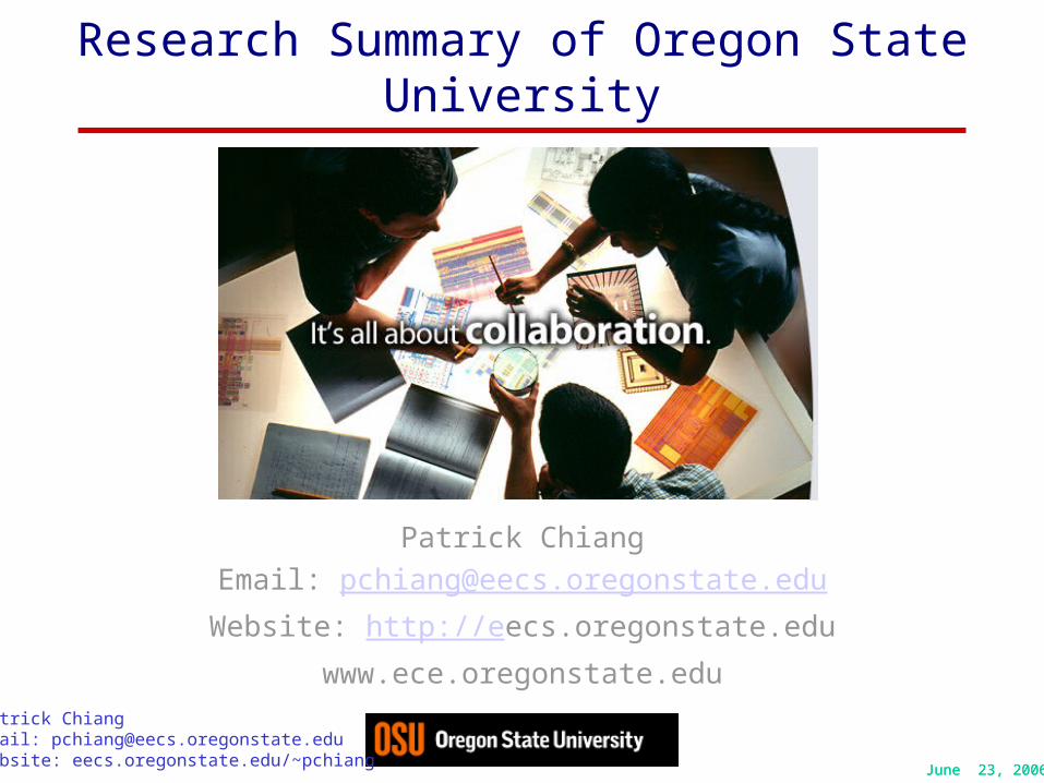
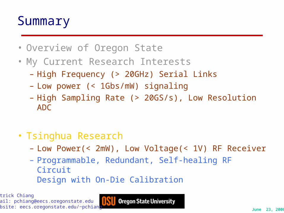
Summary
• Overview of Oregon State • My Current Research Interests
– High Frequency (> 20GHz) Serial Links– Low power (< 1Gbs/mW) signaling– High Sampling Rate (> 20GS/s), Low Resolution
ADC
• Tsinghua Research– Low Power(< 2mW), Low Voltage(< 1V) RF
Receiver– Programmable, Redundant, Self-healing RF Circuit
Design with On-Die Calibration
June 23, 2006June 23, 2006
Patrick ChiangEmail: [email protected]: eecs.oregonstate.edu/~pchiang
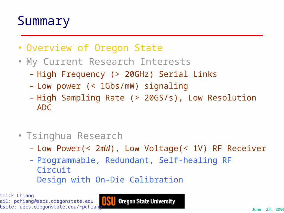
Life at Oregon State University
• Location
• Beautiful surroundings
• Oregon is high tech center– Intel – Mentor Graphics– Synopsys
Main Hall, OSU Mt. Hood, Oregon
Oregon State Stanford, Berkeley
UCLA, Caltech
IntelHillsboro, Oregon
June 23, 2006June 23, 2006
Patrick ChiangEmail: [email protected]: eecs.oregonstate.edu/~pchiang
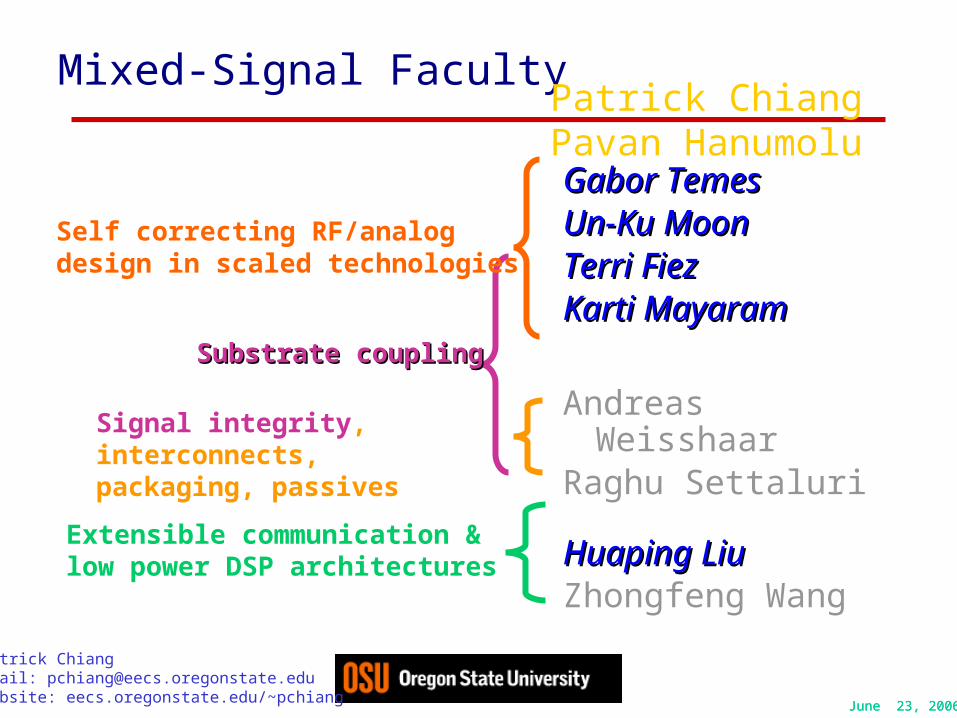
Mixed-Signal Faculty
Gabor TemesGabor TemesUn-Ku MoonUn-Ku MoonTerri FiezTerri FiezKarti MayaramKarti Mayaram
Andreas Weisshaar
Raghu Settaluri
Huaping LiuHuaping LiuZhongfeng Wang
Extensible communication & low power DSP architectures
Signal integrity, interconnects, packaging, passives
Substrate couplingSubstrate coupling
Self correcting RF/analogdesign in scaled technologies
Patrick ChiangPavan Hanumolu
June 23, 2006June 23, 2006
Patrick ChiangEmail: [email protected]: eecs.oregonstate.edu/~pchiang
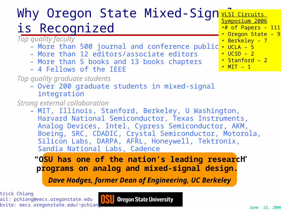
Why Oregon State Mixed-Signalis RecognizedTop quality faculty
– More than 500 journal and conference publications– More than 12 editors/associate editors – More than 5 books and 13 books chapters– 4 Fellows of the IEEE
Top quality graduate students– Over 200 graduate students in mixed-signal integration
Strong external collaboration – MIT, Illinois, Stanford, Berkeley, U Washington, Harvard
National Semiconductor, Texas Instruments, Analog Devices, Intel, Cypress Semiconductor, AKM, Boeing, SRC, CDADIC, Crystal Semiconductor, Motorola, Silicon Labs, DARPA, AFRL, Honeywell, Tektronix, Sandia National Labs, Cadence
“OSU has one of the nation’s leading researchprograms on analog and mixed-signal design.”
Dave Hodges, former Dean of Engineering, UC Berkeley
VLSI Circuits Symposium 2006•# of Papers – 111• Oregon State – 9• Berkeley – 7• UCLA – 5• UCSD – 2• Stanford – 2• MIT – 1
June 23, 2006June 23, 2006
Patrick ChiangEmail: [email protected]: eecs.oregonstate.edu/~pchiang
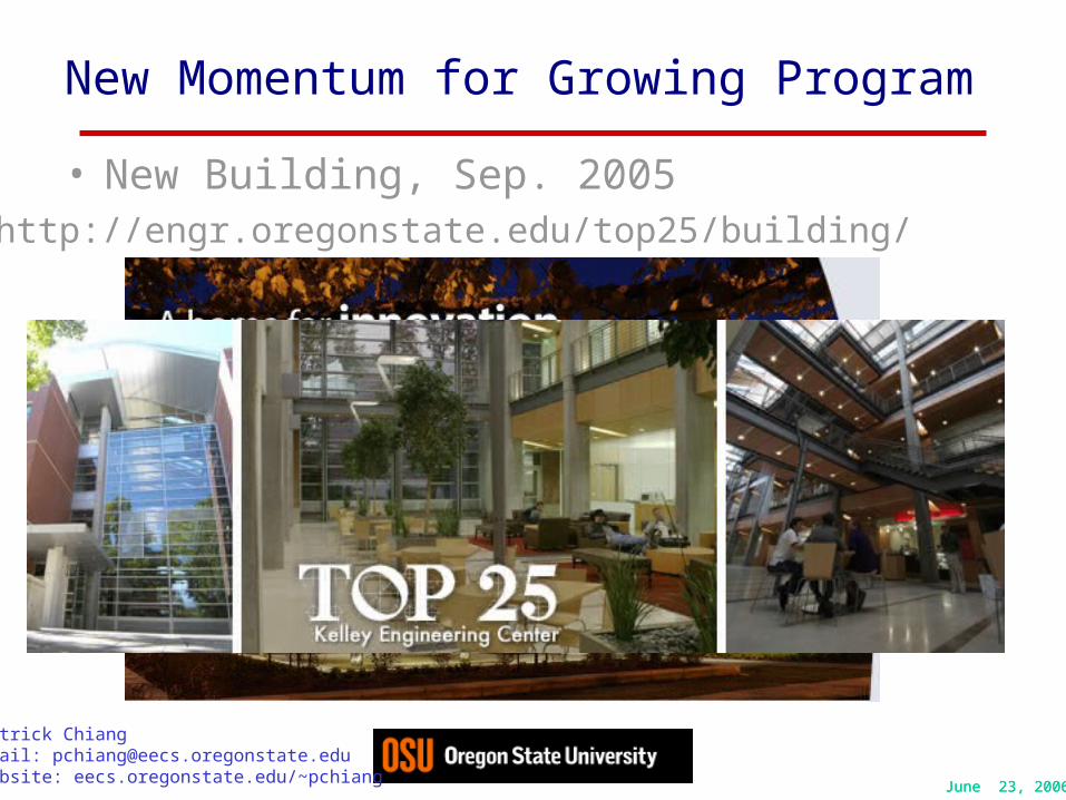
New Momentum for Growing Program
• New Building, Sep. 2005 http://engr.oregonstate.edu/top25/building/
June 23, 2006June 23, 2006
Patrick ChiangEmail: [email protected]: eecs.oregonstate.edu/~pchiang
Summary
• Overview of Oregon State • My Current Research Interests
– High Frequency (> 20GHz) Serial Links– Low power (< 1Gbs/mW) signaling– High Sampling Rate (> 20GS/s), Low Resolution
ADC
• Tsinghua Research– Low Power(< 2mW), Low Voltage(< 1V) RF
Receiver– Programmable, Redundant, Self-healing RF Circuit
Design with On-Die Calibration
June 23, 2006June 23, 2006
Patrick ChiangEmail: [email protected]: eecs.oregonstate.edu/~pchiang
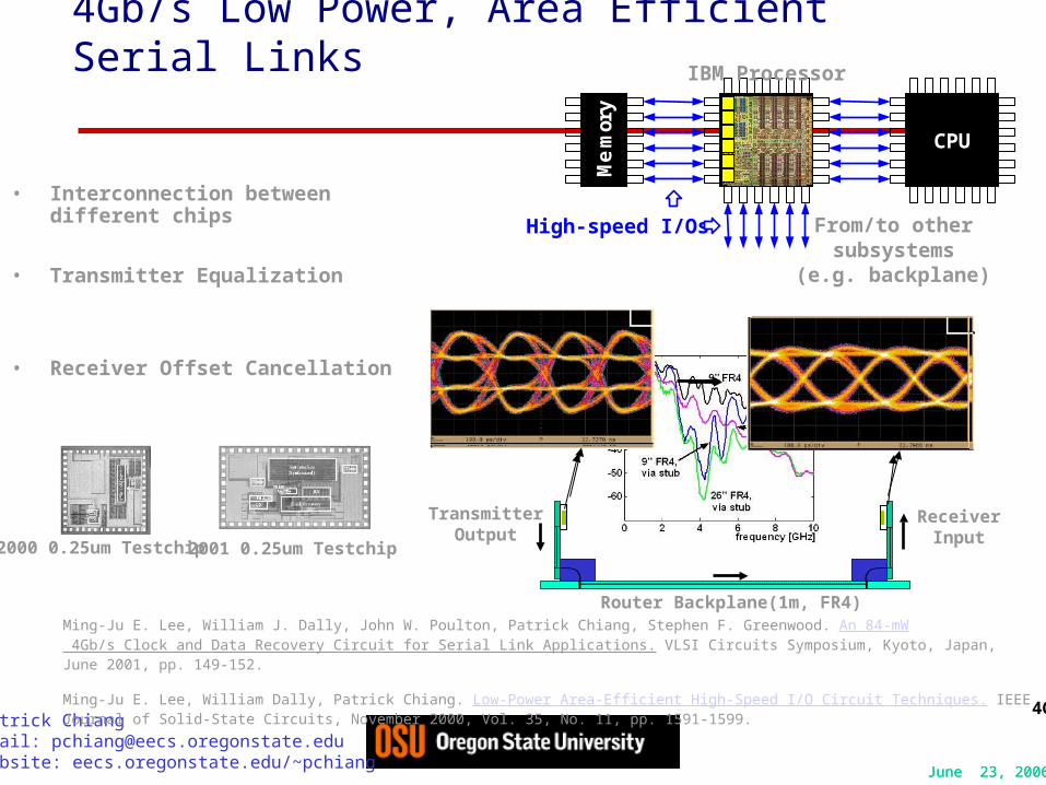
4Gb/s Low Power, Area Efficient Serial Links
• Interconnection betweendifferent chips
• Transmitter Equalization
• Receiver Offset Cancellation
2000 0.25um Testchip 2001 0.25um Testchip
Ming-Ju E. Lee, William J. Dally, John W. Poulton, Patrick Chiang, Stephen F. Greenwood. An 84-mW 4Gb/s Clock and Data Recovery Circuit for Serial Link Applications. VLSI Circuits Symposium, Kyoto, Japan, June 2001, pp. 149-152.
Ming-Ju E. Lee, William Dally, Patrick Chiang. Low-Power Area-Efficient High-Speed I/O Circuit Techniques. IEEE Journal of Solid-State Circuits, November 2000, Vol. 35, No. 11, pp. 1591-1599.
TransmitterOutput
Router Backplane(1m, FR4)
ReceiverInput
CPU CPU
Me
mo
ry
From/to othersubsystems
(e.g. backplane)
High-speed I/Os
IBM Processor
June 23, 2006June 23, 2006
Patrick ChiangEmail: [email protected]: eecs.oregonstate.edu/~pchiang
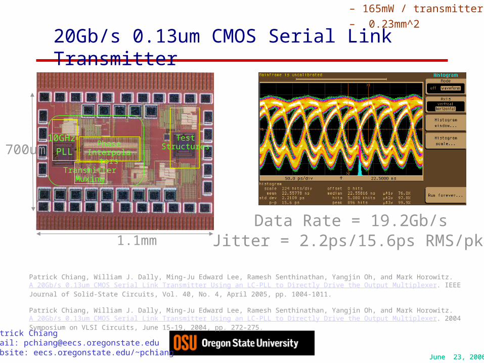
20Gb/s 0.13um CMOS Serial Link Transmitter
Jitter = 2.2ps/15.6ps RMS/pk-pkData Rate = 19.2Gb/s
Clock Recovery
RXPRBS Check
PRBS GenTXDLL
Test Interface
700um
1.1mm
10GHz
PLL
TransmitterMuxing
PhaseInterpolators
TestStructures
– 165mW / transmitter– 0.23mm^2
Patrick Chiang, William J. Dally, Ming-Ju Edward Lee, Ramesh Senthinathan, Yangjin Oh, and Mark Horowitz. A 20Gb/s 0.13um CMOS Serial Link Transmitter Using an LC-PLL to Directly Drive the Output Multiplexer. IEEE Journal of Solid-State Circuits, Vol. 40, No. 4, April 2005, pp. 1004-1011.
Patrick Chiang, William J. Dally, Ming-Ju Edward Lee, Ramesh Senthinathan, Yangjin Oh, and Mark Horowitz. A 20Gb/s 0.13um CMOS Serial Link Transmitter Using an LC-PLL to Directly Drive the Output Multiplexer. 2004 Symposium on VLSI Circuits, June 15-19, 2004, pp. 272-275.
June 23, 2006June 23, 2006
Patrick ChiangEmail: [email protected]: eecs.oregonstate.edu/~pchiang
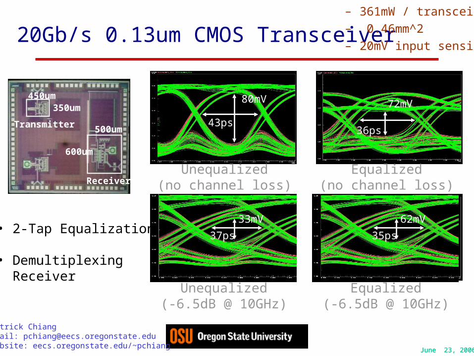
20Gb/s 0.13um CMOS Transceiver– 361mW / transceiver– 0.46mm^2– 20mV input sensitivity
500um
600um
350um450um
Transmitter
Receiver
33mV
37ps
43ps
80mV
62mV
35ps
36ps
72mV
Unequalized(no channel loss)
Unequalized(-6.5dB @ 10GHz)
62mV
35ps
Equalized(no channel loss)
Equalized(-6.5dB @ 10GHz)
• 2-Tap Equalization
• Demultiplexing Receiver
June 23, 2006June 23, 2006
Patrick ChiangEmail: [email protected]: eecs.oregonstate.edu/~pchiang
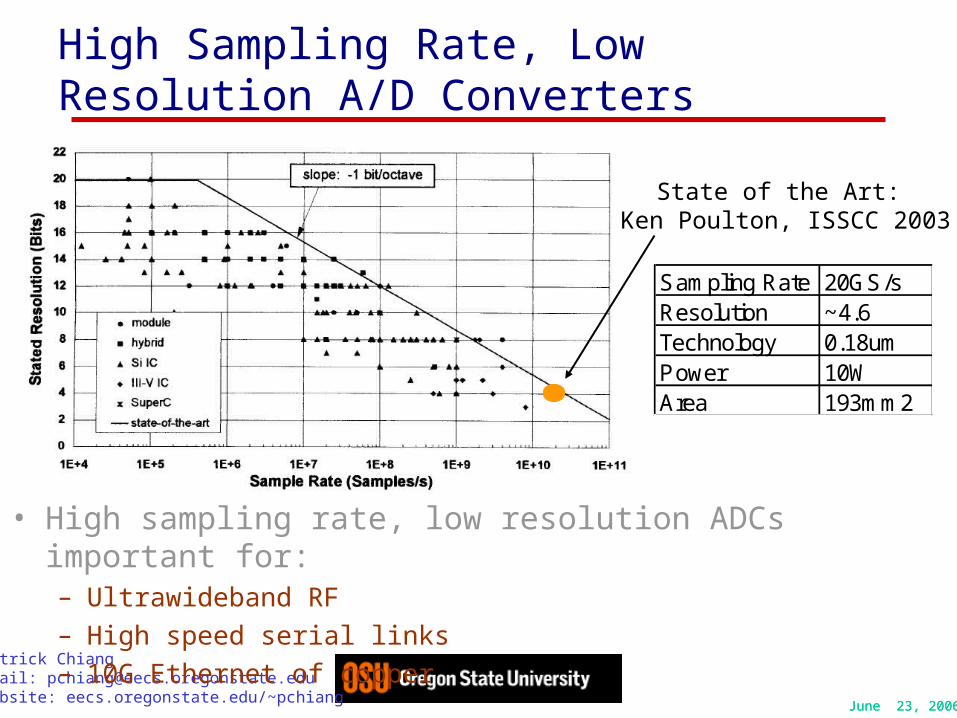
High Sampling Rate, Low Resolution A/D Converters
• High sampling rate, low resolution ADCs important for:– Ultrawideband RF– High speed serial links– 10G Ethernet of copper
State of the Art: Ken Poulton, ISSCC 2003
Sampling Rate 20GS/sResolution ~4.6Technology 0.18umPower 10WArea 193mm2
June 23, 2006June 23, 2006
Patrick ChiangEmail: [email protected]: eecs.oregonstate.edu/~pchiang
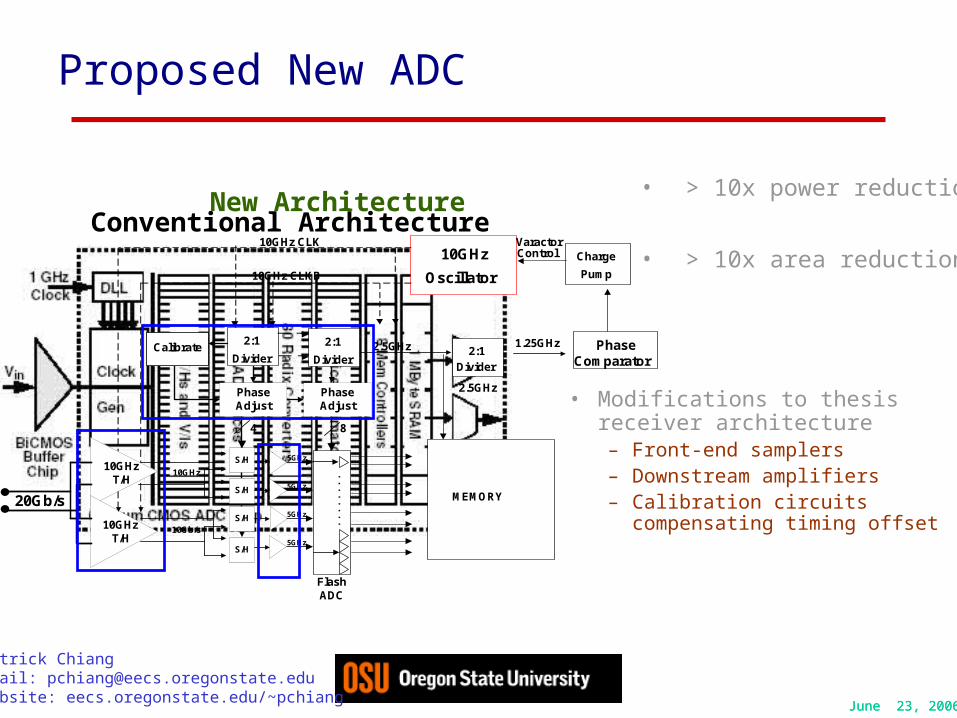
Proposed New ADC
• Modifications to thesis receiver architecture– Front-end samplers– Downstream amplifiers– Calibration circuits
compensating timing offset
• > 10x power reduction
• > 10x area reduction
Conventional Architecture10GHz
Oscillator
20Gb/s
10GHz CLK
10GHz CLKB
PhaseComparator
Charge
Pump
VaractorControl
Divider
2:11.25GHz
2.5GHz
2.5GHz2:1
Divider
10GHz1:25GHz
5GHz
5GHz
2:1
Divider
10GHzT/H
10GHzT/H
10Gb/s
5GHz
8
S/H
S/H
S/H
S/H
FlashADC
MEMORY
PhaseAdjust
PhaseAdjust
4
Calibrate
New Architecture
June 23, 2006June 23, 2006
Patrick ChiangEmail: [email protected]: eecs.oregonstate.edu/~pchiang
Summary
• Overview of Oregon State • My Current Research Interests
– High Frequency (> 20GHz) Serial Links– Low power (< 1Gbs/mW) signaling– High Sampling Rate (> 20GS/s), Low Resolution
ADC
• Tsinghua Research– Low Power(< 2mW), Low Voltage(< 1V) RF
Receiver– Programmable, Redundant, Self-healing RF Circuit
Design with On-Die Calibration
June 23, 2006June 23, 2006
Patrick ChiangEmail: [email protected]: eecs.oregonstate.edu/~pchiang
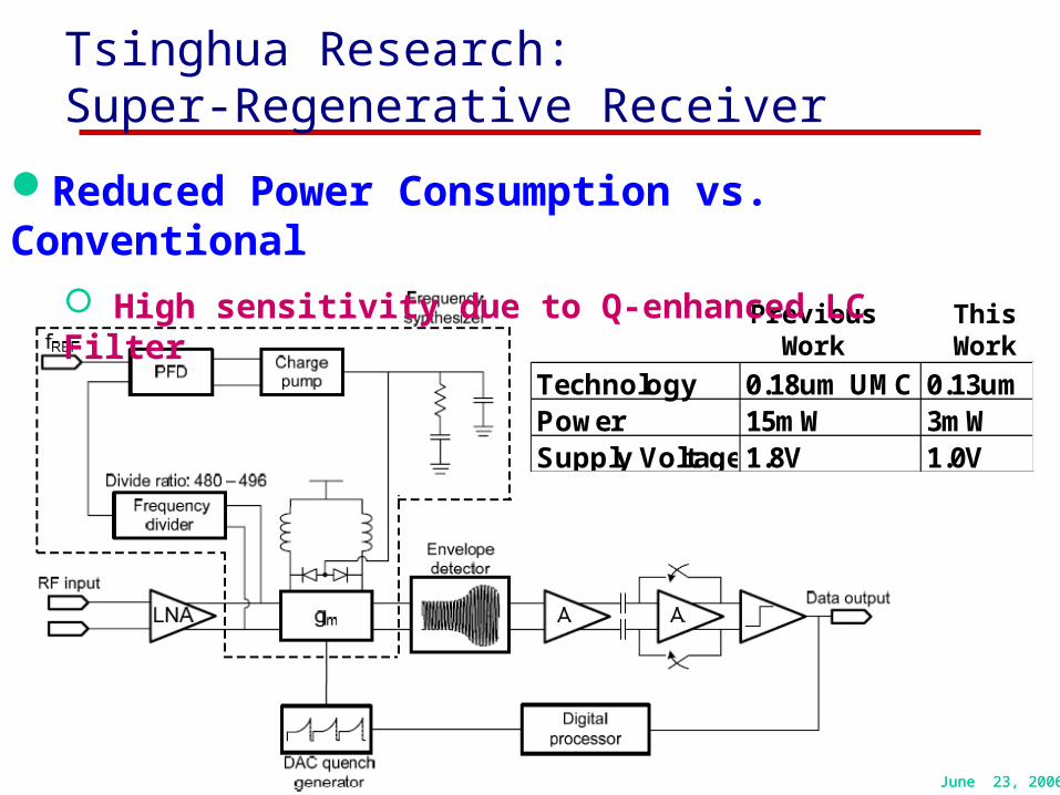
Tsinghua Research: Super-Regenerative Receiver
Technology 0.18um UMC 0.13umPower 15mW 3mWSupply Voltage1.8V 1.0V
PreviousWork
ThisWork
Reduced Power Consumption vs. Conventional
High sensitivity due to Q-enhanced LC Filter
June 23, 2006June 23, 2006
Patrick ChiangEmail: [email protected]: eecs.oregonstate.edu/~pchiang
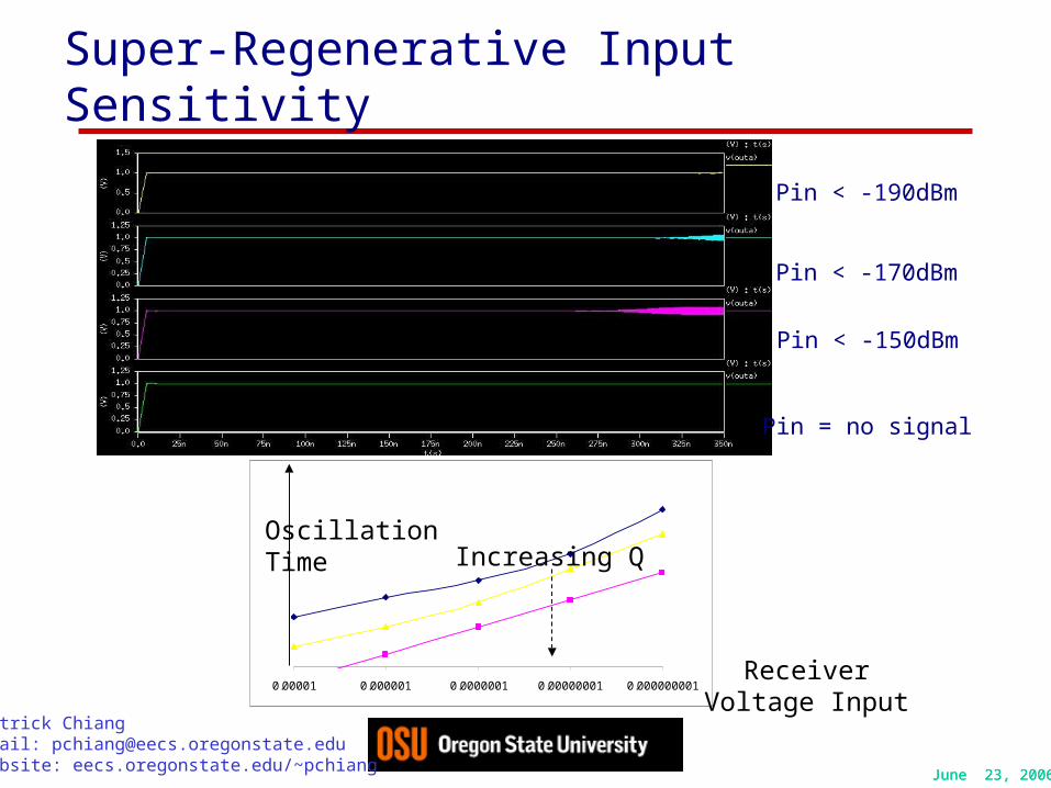
Super-Regenerative Input Sensitivity
Pin = no signal
Pin < -150dBm
Pin < -170dBm
Pin < -190dBm
0.0000000010.000000010.00000010.0000010.00001
OscillationTime Increasing Q
ReceiverVoltage Input
June 23, 2006June 23, 2006
Patrick ChiangEmail: [email protected]: eecs.oregonstate.edu/~pchiang
Summary
• Overview of Oregon State • My Current Research Interests
– High Frequency (> 20GHz) Serial Links– Low power (< 1Gbs/mW) signaling– High Sampling Rate (> 20GS/s), Low Resolution
ADC
• Tsinghua Research(with Dr. Baoyong Chi)– Low Power(< 2mW), Low Voltage(< 1V) RF
Receiver– Programmable, Redundant, Self-healing RF Circuit
Design with On-Die Calibration
June 23, 2006June 23, 2006
Patrick ChiangEmail: [email protected]: eecs.oregonstate.edu/~pchiang
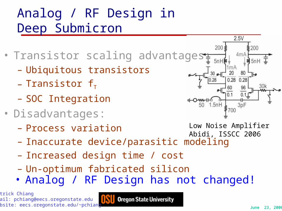
Low Noise AmplifierAbidi, ISSCC 2006
Analog / RF Design in Deep Submicron
• Transistor scaling advantages:– Ubiquitous transistors
– Transistor fT
– SOC Integration
• Disadvantages:– Process variation– Inaccurate device/parasitic modeling– Increased design time / cost– Un-optimum fabricated silicon• Analog / RF Design has not changed!
June 23, 2006June 23, 2006
Patrick ChiangEmail: [email protected]: eecs.oregonstate.edu/~pchiang
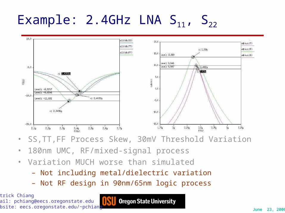
Example: 2.4GHz LNA S11, S22
• SS,TT,FF Process Skew, 30mV Threshold Variation• 180nm UMC, RF/mixed-signal process• Variation MUCH worse than simulated
– Not including metal/dielectric variation– Not RF design in 90nm/65nm logic process
June 23, 2006June 23, 2006
Patrick ChiangEmail: [email protected]: eecs.oregonstate.edu/~pchiang
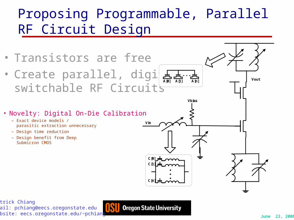
Proposing Programmable, ParallelRF Circuit Design
• Transistors are free• Create parallel, digitally
switchable RF Circuits
• Novelty: Digital On-Die Calibration– Exact device models /
parasitic extraction unnecessary– Design time reduction– Design benefit from Deep
Submicron CMOS
A[0] A[1] A[n]
. . .
. . .
C[0]
C[1]
C[n]
Vin
Vout
Vbias
June 23, 2006June 23, 2006
Patrick ChiangEmail: [email protected]: eecs.oregonstate.edu/~pchiang
Conclusion
• Oregon State is a great place to pursue a
graduate degree
• I am looking for intense, bright students to start
my research group
• Questions?
– Email: [email protected]
– Email: [email protected]