Embed Size (px)
Citation preview
k
Featuresbull Optimized for high-performance 33V systems
- 5 ns pin-to-pin logic delays with internal system frequency up to 208 MHz
- Small footprint packages including VQFPs TQFPs and CSPs (Chip Scale Package)
- Pb-free available for all packages- Lower power operation- 5V tolerant IO pins accept 5V 33V and 25V
signals- 33V or 25V output capability- Advanced 035 micron feature size CMOS
FastFLASH technologybull Advanced system features
- In-system programmable- Superior pin-locking and routability with
FastCONNECT IItrade switch matrix- Extra wide 54-input Function Blocks- Up to 90 product-terms per macrocell with
individual product-term allocation
- Local clock inversion with three global and one product-term clocks
- Individual output enable per output pin with local inversion
- Input hysteresis on all user and boundary-scan pin inputs
- Bus-hold circuitry on all user pin inputs- Supports hot-plugging capability- Full IEEE Standard 11491 boundary-scan (JTAG)
support on all devicesbull Four pin-compatible device densities
- 36 to 288 macrocells with 800 to 6400 usable gates
bull Fast concurrent programming bull Slew rate control on individual outputsbull Enhanced data security featuresbull Excellent quality and reliability
- 10000 programerase cycles endurance rating- 20 year data retention
bull Pin-compatible with 5V core XC9500 family in common package footprints
0
XC9500XL High-Performance CPLD Family Data Sheet
DS054 (v19) November 11 2004 0 0 Preliminary Product Specification
R
Table 1 XC9500XL Device FamilyXC9536XL XC9572XL XC95144XL XC95288XL
Macrocells 36 72 144 288
Usable Gates 800 1600 3200 6400
Registers 36 72 144 288
TPD (ns) 5 5 5 6
TSU (ns) 37 37 37 40
TCO (ns) 35 35 35 38
fSYSTEM (MHz) 178 178 178 208
DS054 (v19) November 11 2004 wwwxilinxcom 1Preliminary Product Specification 1-800-255-7778
copy 2004 Xilinx Inc All rights reserved All Xilinx trademarks registered trademarks patents and disclaimers are as listed at httpwwwxilinxcomlegalhtm All other trademarks and registered trademarks are the property of their respective owners All specifications are subject to change without notice
XC9500XL High-Performance CPLD Family Data Sheet R
Table 2 XC9500XL Packages and User IO Pins (not including 4 dedicated JTAG pins)Package(1) XC9536XL XC9572XL XC95144XL XC95288XL
PC44 34 34 - -
PCG44 34 34
VQ44 34 34 - -
VQG44 34 34
CS48 36 38 - -
CSG48 36 38
VQ64 36 52 - -
VQG64 36 52
TQ100 - 72 81 -
TQG100 72 81
CS144 - - 117 -
CSG144 117
TQ144 - - 117 117
TQG144 117 117
PQ208 - - - 168
PQG208 168
BG256 - - - 192
BGG256 192
FG256 - - - 192
FGG256 192
CS280 - - - 192
CSG280 192
Notes (1) The letter G as the third character indicates a Pb-free package
2 wwwxilinxcom DS054 (v19) November 11 20041-800-255-7778 Preliminary Product Specification
XC9500XL High-Performance CPLD Family Data SheetR
Family OverviewThe FastFLASH XC9500XL family is a 33V CPLD familytargeted for high-performance low-voltage applications inleading-edge communications and computing systemswhere high device reliability and low power dissipation isimportant Each XC9500XL device supports in-system pro-gramming (ISP) and the full IEEE 11491 (JTAG) bound-ary-scan allowing superior debug and design iterationcapability for small form-factor packages The XC9500XLfamily is designed to work closely with the Xilinx VirtexSpartan-XL and XC4000XL FPGA families allowing systemdesigners to partition logic optimally between fast interfacecircuitry and high-density general purpose logic As shownin Table 1 logic density of the XC9500XL devices rangesfrom 800 to 6400 usable gates with 36 to 288 registersrespectively Multiple package options and associated IO
capacity are shown in Table 2 The XC9500XL family mem-bers are fully pin-compatible allowing easy design migra-tion across multiple density options in a given packagefootprint
The XC9500XL architectural features address the require-ments of in-system programmability Enhanced pin-lockingcapability avoids costly board rework In-system program-ming throughout the full commercial operating range and ahigh programming endurance rating provide worry-freereconfigurations of system field upgrades Extended dataretention supports longer and more reliable system operat-ing life
Advanced system features include output slew rate controland user-programmable ground pins to help reduce systemnoise Each user pin is compatible with 5V 33V and 25Vinputs and the outputs may be configured for 33V or 25V
Figure 1 XC9500XL ArchitectureNote Function block outputs (indicated by the bold lines) drive the IO blocks directly
In-System Programming ControllerJTAGController
IOBlocks
FunctionBlock 1
Macrocells1 to 18
Macrocells1 to 18
Macrocells1 to 18
Macrocells1 to 18
JTAG Port
3
54
IOGTS
IOGSR
IOGCK
IO
IO
IO
IO
2 or 4
1
IO
IO
IO
IO
3
DS054_01_042001
FunctionBlock 2
54
FunctionBlock 3
54
18
18
18
18FunctionBlock N
54F
astC
ON
NE
CT
II S
witc
h M
atrix
DS054 (v19) November 11 2004 wwwxilinxcom 3Preliminary Product Specification 1-800-255-7778
XC9500XL High-Performance CPLD Family Data Sheet R
operation The XC9500XL device exhibits symmetric full33V output voltage swing to allow balanced rise and falltimes Additional details can be found in the applicationnotes listed in Further Reading on page 17
Architecture DescriptionEach XC9500XL device is a subsystem consisting of multi-ple Function Blocks (FBs) and IO Blocks (IOBs) fully inter-connected by the FastCONNECT II switch matrix The IOBprovides buffering for device inputs and outputs Each FBprovides programmable logic capability with extra wide54inputs and 18 outputs The FastCONNECT II switchmatrix connects all FB outputs and input signals to the FBinputs For each FB up to 18 outputs (depending on pack-age pin-count) and associated output enable signals drivedirectly to the IOBs See Figure 1
Function BlockEach Function Block as shown in Figure 2 is comprised of18 independent macrocells each capable of implementinga combinatorial or registered function The FB also receivesglobal clock output enable and setreset signals The FBgenerates 18 outputs that drive the FastCONNECT switchmatrix These 18 outputs and their corresponding outputenable signals also drive the IOB
Logic within the FB is implemented using a sum-of-productsrepresentation Fifty-four inputs provide 108 true and com-plement signals into the programmable AND-array to form90 product terms Any number of these product terms up tothe 90 available can be allocated to each macrocell by theproduct term allocator
MacrocellEach XC9500XL macrocell may be individually configuredfor a combinatorial or registered function The macrocelland associated FB logic is shown in Figure 3
Five direct product terms from the AND-array are availablefor use as primary data inputs (to the OR and XOR gates) toimplement combinatorial functions or as control inputs
including clock clock enable setreset and output enableThe product term allocator associated with each macrocellselects how the five direct terms are used
The macrocell register can be configured as a D-type orT-type flip-flop or it may be bypassed for combinatorialoperation Each register supports both asynchronous setand reset operations During power-up all user registers
Figure 2 XC9500XL Function Block
Macrocell 18
Macrocell 1
ProgrammableAND-Array
ProductTerm
AllocatorsFrom
FastCONNECT IISwitch Matrix
DS054_02_042101
54
1
To FastCONNECT IISwitch Matrix
To IO BlocksOUT
GlobalSetReset
3
18
PTOE18
18
GlobalClocks
4 wwwxilinxcom DS054 (v19) November 11 20041-800-255-7778 Preliminary Product Specification
XC9500XL High-Performance CPLD Family Data SheetR
are initialized to the user-defined preload state (default to 0if unspecified)
All global control signals are available to each individualmacrocell including clock setreset and output enable sig-nals As shown in Figure 4 the macrocell register clockoriginates from either of three global clocks or a product
term clock Both true and complement polarities of theselected clock source can be used within each macrocell AGSR input is also provided to allow user registers to be setto a user-defined state
Figure 3 XC9500XL Macrocell Within Function Block
DS054_03_042101
ToFastCONNECTIISwitch Matrix
AdditionalProductTerms(from othermacrocells)
GlobalSetReset
GlobalClocks
AdditionalProductTerms(from othermacrocells)
To IO Blocks
OUT
1
0
54
3
PTOE
DT QS
R
ProductTerm
Allocator
Product Term Set
Product Term Clock
Product Term Reset
Product Term OE
Product Term Clock Enable
CE
DS054 (v19) November 11 2004 wwwxilinxcom 5Preliminary Product Specification 1-800-255-7778
XC9500XL High-Performance CPLD Family Data Sheet R
Figure 4 Macrocell Clock and SetReset Capability
DTCE
S
R
Macrocell
DS05404_042101
IOGSR
Product Term Set
Product Term Clock
Product Term Reset
Global SetReset
Global Clock 1
Global Clock 2
Global Clock 3IOGCK3
IOGCK2
IOGCK1
6 wwwxilinxcom DS054 (v19) November 11 20041-800-255-7778 Preliminary Product Specification
XC9500XL High-Performance CPLD Family Data SheetR
Product Term AllocatorThe product term allocator controls how the five direct prod-uct terms are assigned to each macrocell For example allfive direct terms can drive the OR function as shown inFigure 5
The product term allocator can re-assign other productterms within the FB to increase the logic capacity of a mac-rocell beyond five direct terms Any macrocell requiringadditional product terms can access uncommitted productterms in other macrocells within the FB Up to 15 productterms can be available to a single macrocell with only asmall incremental delay of tPTA as shown in Figure 6
Note that the incremental delay affects only the productterms in other macrocells The timing of the direct productterms is not changed
Figure 5 Macrocell Logic Using Direct Product Term
Product TermAllocator
MacrocellProduct TermLogic
DS054_05_042101
Figure 6 Product Term Allocation With 15 Product Terms
Macrocell LogicWith 15 Product Terms
Product TermAllocator
Product TermAllocator
DS054_06_042101
Product TermAllocator
DS054 (v19) November 11 2004 wwwxilinxcom 7Preliminary Product Specification 1-800-255-7778
XC9500XL High-Performance CPLD Family Data Sheet R
The product term allocator can re-assign product termsfrom any macrocell within the FB by combining partial sumsof products over several macrocells as shown in Figure 7In this example the incremental delay is only 2TPTA All 90product terms are available to any macrocell with a maxi-mum incremental delay of 8TPTA
Figure 7 Product Term Allocation Over Several Macrocells
Macrocell LogicWith 18Product Terms
Macrocell LogicWith 2Product Terms
Product TermAllocator
Product TermAllocator
DS054_07 _042101
Product TermAllocator
Product TermAllocator
8 wwwxilinxcom DS054 (v19) November 11 20041-800-255-7778 Preliminary Product Specification
XC9500XL High-Performance CPLD Family Data SheetR
The internal logic of the product term allocator is shown inFigure 8
Figure 8 Product Term Allocator Logic
DT QS
R
From UpperMacrocell
To UpperMacrocell
Product Term Set
Product Term Clock
Product Term Reset
Global SetReset
Global SetReset
Global Clocks
Product Term OE
Product TermAllocator
To LowerMacrocell
From LowerMacrocell
DS054_08_042101
1
0
CE
DS054 (v19) November 11 2004 wwwxilinxcom 9Preliminary Product Specification 1-800-255-7778
XC9500XL High-Performance CPLD Family Data Sheet R
FastCONNECT II Switch MatrixThe FastCONNECT II Switch Matrix connects signals to theFB inputs as shown in Figure 9 All IOB outputs (corre-
sponding to user pin inputs) and all FB outputs drive theFastCONNECT II matrix Any of these (up to a fan-in limit of54) may be selected to drive each FB with a uniform delay
Figure 9 FastCONNECT II Switch Matrix
DS054_09_042101
Function Block
FastCONNECT IISwitch Matrix
(54)
IO
Function Block
IO Block
18
18
IO Block
(54)
IO
DT Q
DT Q
10 wwwxilinxcom DS054 (v19) November 11 20041-800-255-7778 Preliminary Product Specification
XC9500XL High-Performance CPLD Family Data SheetR
IO BlockThe IO Block (IOB) interfaces between the internal logicand the device user IO pins Each IOB includes an input
buffer output driver output enable selection multiplexerand user programmable ground control See Figure 10 fordetails
The input buffer is compatible with 5V CMOS 5V TTL 33VCMOS and 25V CMOS signals The input buffer uses theinternal 33V voltage supply (VCCINT) to ensure that theinput thresholds are constant and do not vary with the VCCIOvoltage Each input buffer provides input hysteresis (50 mV
typical) to help reduce system noise for input signals withslow rise or fall edges
Each output driver is designed to provide fast switching withminimal power noise All output drivers in the device may be
Figure 10 IO Block and Output Enable Capability
IO Block
Macrocell
DS054_10_042101
Product Term OE PTOE
Switch Matrix
OUT
(Inversion inAND-array)
Global OE 1
1
To otherMacrocells
Slew RateControl
0
Global OE 2
Available in XC95144XLand XC95288XLGlobal OE 3
Global OE 4
IOGTS1
IO
IOGTS2
IOGTS3
IOGTS4
To FastCONNECT
User-Programmable
Ground
Bus-Hold
DS054 (v19) November 11 2004 wwwxilinxcom 11Preliminary Product Specification 1-800-255-7778
XC9500XL High-Performance CPLD Family Data Sheet R
configured for driving either 33V CMOS levels (which arecompatible with 5V TTL levels as well) or 25V CMOS levelsby connecting the device output voltage supply (VCCIO) to a33V or 25V voltage supply Figure 11 shows how theXC9500XL device can be used in 33V only systems andmixed voltage systems with any combination of 5V 33Vand 25V power supplies
Each output driver can also be configured for slew-rate lim-ited operation Output edge rates may be slowed down toreduce system noise (with an additional time delay of tSLEW)under user control See Figure 12
The output enable may be generated from one of fouroptions a product term signal from the macrocell any of theglobal output enable signals (GTS) always ldquo1rdquo or alwaysldquo0rdquo There are two global output enables for devices with 72or fewer macrocells and four global output enables fordevices with 144 or more macrocells Any selected outputenable signal may be inverted locally at each pin output toprovide maximal design flexibility
Each IOB provides user programmable ground pin capabil-ity This allows device IO pins to be configured as additionalground pins in order to force otherwise unused pins to a lowvoltage state as well as provide for additional device
grounding capability This grounding of the pin is achievedby internal logic that forces a logic low output regardless ofthe internal macrocell signal so the internal macrocell logicis unaffected by the programmable ground pin capability
Each IOB also provides for bus-hold circuitry (also called aldquokeeperrdquo)that is active during valid user operation Thebus-hold feature eliminates the need to tie unused pinseither high or low by holding the last known state of the inputuntil the next input signal is present The bus-hold circuitdrives back the same state via a nominal resistance (RBH)of 50k ohms See Figure 13 Note the bus-hold output willdrive no higher than VCCIO to prevent overdriving signalswhen interfacing to 25V components
When the device is not in valid user operation the bus-holdcircuit defaults to an equivalent 50k ohm pull-up resistor inorder to provide a known repeatable device state Thisoccurs when the device is in the erased state in program-ming mode in JTAG INTEST mode or during initialpower-up A pull-down resistor (1k ohm) may be externallyadded to any pin to override the default RBH resistance toforce a low state during power-up or any of these othermodes
5V Tolerant IOsThe IOs on each XC9500XL device are fully 5V toleranteven though the core power supply is 33 volts This allows5V CMOS signals to connect directly to the XC9500XLinputs without damage In addition the 33V VCCINT powersupply can be applied before or after 5V signals are appliedto the IOs In mixed 5V33V25V systems the user pinsthe core power supply (VCCINT) and the output power sup-ply (VCCIO) may have power applied in any order Thismakes the XC9500XL devices immune to power supplysequencing problems
Xilinx proprietary ESD circuitry and high impedance initialstate permit hot plugging cards using these devices
Pin-Locking CapabilityThe capability to lock the user defined pin assignments dur-ing design iteration depends on the ability of the architec-ture to adapt to unexpected changes The XC9500XLdevices incorporate architectural features that enhance theability to accept design changes while maintaining the samepinout
Figure 11 XC9500XL Devices in (a) 33V only and (b) Mixed 5V33V25V Systems
IN OUT
25V33V
GND
(b)
25V CMOS
IN OUT
XC9500XLCPLD
XC9500XLCPLD
VCCINT VCCIO VCCINT VCCIO
33V
GND
(a)
33V
0V
5V
0V
33V
0V
25V
0V
25V
0V
33V CMOS 5V TTL
DS054_11_042101
25V CMOS
33V CMOS or
5V TTL or
5V
0V
5V CMOS
5V
0V
33V
0V
25V
0V
25V CMOS
33V CMOS or
5V TTL or
5V
0V
5V CMOS
12 wwwxilinxcom DS054 (v19) November 11 20041-800-255-7778 Preliminary Product Specification
XC9500XL High-Performance CPLD Family Data SheetR
The XC9500XL architecture provides for superior pin-lock-ing characteristics with a combination of large number ofrouting switches in the FastCONNECT II switch matrix a54-wide input Function Block and flexible bi-directionalproduct term allocation within each macrocell These fea-tures address design changes that require adding or chang-ing internal routing including additional signals into existingequations or increasing equation complexity respectively
For extensive design changes requiring higher logic capac-ity than is available in the initially chosen device the newdesign may be able to fit into a larger pin-compatible deviceusing the same pin assignments The same board may beused with a higher density device without the expense ofboard rework
In-System ProgrammingOne or more XC9500XL devices can be daisy chainedtogether and programmed in-system via a standard 4-pinJTAG protocol as shown in Figure 14 In-system program-ming offers quick and efficient design iterations and elimi-nates package handling The Xilinx development systemprovides the programming data sequence using a Xilinxdownload cable a third-party JTAG development systemJTAG-compatible board tester or a simple microprocessorinterface that emulates the JTAG instruction sequence
All IOs are 3-stated and pulled high by the bus-hold cir-cuitry during in-system programming If a particular signalmust remain low during this time then a pulldown resistormay be added to the pin
External ProgrammingXC9500XL devices can also be programmed by the XilinxHW-130 device programmer as well as third-party program-mers This provides the added flexibility of using pre-pro-grammed devices during manufacturing with an in-systemprogrammable option for future enhancements and designchanges
Reliability and EnduranceAll XC9500XL CPLDs provide a minimum endurance levelof 10000 in-system programerase cycles and a minimumdata retention of 20 years Each device meets all functionalperformance and data retention specifications within thisendurance limit
IEEE 11491 Boundary-Scan (JTAG)XC9500XL devices fully support IEEE 11491 bound-ary-scan (JTAG) EXTEST SAMPLEPRELOAD BYPASSUSERCODE INTEST IDCODE HIGHZ and CLAMPinstructions are supported in each device Additionalinstructions are included for in-system programming opera-tions
Figure 12 Output Slew-Rate Control For (a) Rising and (b) Falling Outputs
Time0 0
15V
Standard
OutputVoltage
(a)
Slew-Rate Limited
Time
OutputVoltage
(b)
Standard
Slew-Rate Limited
VCCIO
TSLEW TSLEW
15V
DS054_12_042101
Figure 13 Bus-Hold Logic
RBH
IO
Set to PINduring valid useroperation Drive to
VCCIO Level
PIN
0
DS054_13_042101
DS054 (v19) November 11 2004 wwwxilinxcom 13Preliminary Product Specification 1-800-255-7778
XC9500XL High-Performance CPLD Family Data Sheet R
Design SecurityXC9500XL devices incorporate advanced data security fea-tures which fully protect the programming data againstunauthorized reading or inadvertent device erasurerepro-gramming Table 3 shows the four different security settingsavailable
The read security bits can be set by the user to prevent theinternal programming pattern from being read or copiedWhen set they also inhibit further program operations butallow device erase Erasing the entire device is the only wayto reset the read security bit
The write security bits provide added protection againstaccidental device erasure or reprogramming when theJTAG pins are subject to noise such as during systempower-up Once set the write-protection may be deacti-
vated when the device needs to be reprogrammed with avalid pattern with a specific sequence of JTAG instructions
Low Power Mode All XC9500XL devices offer a low-power mode for individualmacrocells or across all macrocells This feature allows thedevice power to be significantly reduced
Each individual macrocell may be programmed inlow-power mode by the user Performance-critical parts ofthe application can remain in standard power mode whileother parts of the application may be programmed forlow-power operation to reduce the overall power dissipa-tion Macrocells programmed for low-power mode incuradditional delay (tLP) in pin-to-pin combinatorial delay aswell as register setup time Product term clock to output andproduct term output enable delays are unaffected by themacrocell power-setting Signals switching at rates lessthan 50 ns risefall time should be assigned to the macro-cells configured in low power mode
Timing ModelThe uniformity of the XC9500XL architecture allows a sim-plified timing model for the entire device The basic timingmodel shown in Figure 15 is valid for macrocell functionsthat use the direct product terms only with standard powersetting and standard slew rate setting Table 4 shows howeach of the key timing parameters is affected by the productterm allocator (if needed) low-power setting and slew-lim-ited setting
The product term allocation time depends on the logic spanof the macrocell function which is defined as one less thanthe maximum number of allocators in the product term pathIf only direct product terms are used then the logic span is0 The example in Figure 6 shows that up to 15 productterms are available with a span of 1 In the case of Figure 7the 18 product term function has a span of 2
Table 3 Data Security Options
Read Security
Default Set
Writ
e Se
curit
y DefaultRead AllowedProgramErase
Allowed
Read InhibitedProgram Inhibited
Erase Allowed
SetRead AllowedProgramErase
Allowed
Read InhibitedProgramErase
Inhibited
Figure 14 System Programming Operation (a) Solder Device to PCB and (b) Program Using Download Cable
X5902
GND
V CC
(a) (b)
14 wwwxilinxcom DS054 (v19) November 11 20041-800-255-7778 Preliminary Product Specification
XC9500XL High-Performance CPLD Family Data SheetR
Detailed timing information may be derived from the full tim-ing model shown in Figure 16 The values and explanations
for each parameter are given in the individual device datasheets
Figure 15 Basic Timing Model
Figure 16 Detailed Timing Model
CombinatorialLogic
Propagation Delay = TPD(a)
CombinatorialLogic
Setup Time = TSU
TCO
TPSU
TPCO
Clock to Out Time = TCO(b)
DT Q
CombinatorialLogic
Internal System Cycle Time = TSYSTEM
DS054_15_042101
(d)
DT Q
CombinatorialLogic
Setup Time = TPSU Clock to Out Time = TPCO(c)
P-Term ClockPath
DT Q
DT Q
SR
TIN
TLOGILP STPTA
TF
TPDI
TSUI TCOITHI
TAOITRAI
TOUT
TSLEW
TEN
DS054_16_042101
TLOGI
TPTCK
TPTSR
TPTTS
TGCK
TGSR
TGTS
Macrocell
CE
DS054 (v19) November 11 2004 wwwxilinxcom 15Preliminary Product Specification 1-800-255-7778
XC9500XL High-Performance CPLD Family Data Sheet R
Power-Up CharacteristicsThe XC9500XL devices are well behaved under all operat-ing conditions During power-up each XC9500XL deviceemploys internal circuitry which keeps the device in the qui-escent state until the VCCINT supply voltage is at a safe level(approximately 25V) During this time all device pins andJTAG pins are disabled and all device outputs are disabledwith the pins weakly pulled high as shown in Table 5 Whenthe supply voltage reaches a safe level all user registersbecome initialized (typically within 200 micros) and the deviceis immediately available for operation as shown inFigure 17
If the device is in the erased state (before any user patternis programmed) the device outputs remain disabled withweak pull-up The JTAG pins are enabled to allow thedevice to be programmed at any time All devices areshipped in the erased state from the factory
If the device is programmed the device inputs and outputstake on their configured states for normal operation TheJTAG pins are enabled to allow device erasure or bound-ary-scan tests at any time
Development System SupportThe XC9500XL family and associated in-system program-ming capabilities are fully supported in either software solu-tions available from Xilinx
The Foundation Series is an all-in-one development systemcontaining schematic entry HDL (VHDL Verilog and
ABEL) and simulation capabilities It supports theXC9500XL family as well as other CPLD and FPGA fami-lies
The Alliance Series includes CPLD and FPGA implementa-tion technology as well as all necessary libraries and inter-faces for Alliance partner EDA solutions
FastFLASH TechnologyAn advanced 035 micron feature size CMOS Flash process isused to fabricate all XC9500XL devices The FastFLASH pro-cess provides high performance logic capability fast pro-gramming times and superior reliability and enduranceratings
Figure 17 Device Behavior During Power-up
VCCINT
NoPower
38 V(Typ)
0VNo
PowerQuiescent
StateQuiescent
StateUser Operation
Initialization of User Registers
DS054_17_042101
25V(Typ)
Table 4 Timing Model Parameters
Parameter DescriptionProduct TermAllocator(1)
MacrocellLow-Power Setting
Output Slew-Limited
SettingTPD Propagation Delay + TPTA S + TLP + TSLEWTSU Global Clock Setup Time + TPTA S + TLP ndashTCO Global Clock-to-output - - + TSLEWTPSU Product Term Clock Setup Time + TPTA S + TLP -TPCO Product Term Clock-to-output - - + TSLEW
TSYSTEM Internal System Cycle Period + TPTA S + TLP -Notes 1 S = the logic span of the function as defined in the text
Table 5 XC9500XL Device CharacteristicsDevice Circuitry Quiescent State Erased Device Operation Valid User Operation
IOB Bus-Hold Pull-up Pull-up Bus-HoldDevice Outputs Disabled Disabled As ConfiguredDevice Inputs and Clocks Disabled Disabled As ConfiguredFunction Block Disabled Disabled As ConfiguredJTAG Controller Disabled Enabled Enabled
16 wwwxilinxcom DS054 (v19) November 11 20041-800-255-7778 Preliminary Product Specification
XC9500XL High-Performance CPLD Family Data SheetR
Further ReadingThe following Xilinx links go to relevant XC9500XL CPLDdocumentation
Data Sheets Application Notes and White PapersPackagingOnline Store
Revision HistoryThe following table shows the revision history for this document
Date Version Revision
092898 10 Initial Xilinx release
100298 11 Figure 1 correction
020399 12 Included hot socket reference revised layout BGA package change for XC95288XL
040299 13 Minor typesetting corrections
060799 14 Minor typesetting corrections
060799 15 Added CS280 package
012502 16 Added DS054 data sheet number Added 44-pin VQFP package Updated Device Family table
020703 17 Added Further Reading section
080204 18 Added Pb-free documentation
111104 19 Changes to package designations in Table 2 on page 2
DS054 (v19) November 11 2004 wwwxilinxcom 17Preliminary Product Specification 1-800-255-7778
XC9500XL High-Performance CPLD Family Data Sheet R
Table 2 XC9500XL Packages and User IO Pins (not including 4 dedicated JTAG pins)Package(1) XC9536XL XC9572XL XC95144XL XC95288XL
PC44 34 34 - -
PCG44 34 34
VQ44 34 34 - -
VQG44 34 34
CS48 36 38 - -
CSG48 36 38
VQ64 36 52 - -
VQG64 36 52
TQ100 - 72 81 -
TQG100 72 81
CS144 - - 117 -
CSG144 117
TQ144 - - 117 117
TQG144 117 117
PQ208 - - - 168
PQG208 168
BG256 - - - 192
BGG256 192
FG256 - - - 192
FGG256 192
CS280 - - - 192
CSG280 192
Notes (1) The letter G as the third character indicates a Pb-free package
2 wwwxilinxcom DS054 (v19) November 11 20041-800-255-7778 Preliminary Product Specification
XC9500XL High-Performance CPLD Family Data SheetR
Family OverviewThe FastFLASH XC9500XL family is a 33V CPLD familytargeted for high-performance low-voltage applications inleading-edge communications and computing systemswhere high device reliability and low power dissipation isimportant Each XC9500XL device supports in-system pro-gramming (ISP) and the full IEEE 11491 (JTAG) bound-ary-scan allowing superior debug and design iterationcapability for small form-factor packages The XC9500XLfamily is designed to work closely with the Xilinx VirtexSpartan-XL and XC4000XL FPGA families allowing systemdesigners to partition logic optimally between fast interfacecircuitry and high-density general purpose logic As shownin Table 1 logic density of the XC9500XL devices rangesfrom 800 to 6400 usable gates with 36 to 288 registersrespectively Multiple package options and associated IO
capacity are shown in Table 2 The XC9500XL family mem-bers are fully pin-compatible allowing easy design migra-tion across multiple density options in a given packagefootprint
The XC9500XL architectural features address the require-ments of in-system programmability Enhanced pin-lockingcapability avoids costly board rework In-system program-ming throughout the full commercial operating range and ahigh programming endurance rating provide worry-freereconfigurations of system field upgrades Extended dataretention supports longer and more reliable system operat-ing life
Advanced system features include output slew rate controland user-programmable ground pins to help reduce systemnoise Each user pin is compatible with 5V 33V and 25Vinputs and the outputs may be configured for 33V or 25V
Figure 1 XC9500XL ArchitectureNote Function block outputs (indicated by the bold lines) drive the IO blocks directly
In-System Programming ControllerJTAGController
IOBlocks
FunctionBlock 1
Macrocells1 to 18
Macrocells1 to 18
Macrocells1 to 18
Macrocells1 to 18
JTAG Port
3
54
IOGTS
IOGSR
IOGCK
IO
IO
IO
IO
2 or 4
1
IO
IO
IO
IO
3
DS054_01_042001
FunctionBlock 2
54
FunctionBlock 3
54
18
18
18
18FunctionBlock N
54F
astC
ON
NE
CT
II S
witc
h M
atrix
DS054 (v19) November 11 2004 wwwxilinxcom 3Preliminary Product Specification 1-800-255-7778
XC9500XL High-Performance CPLD Family Data Sheet R
operation The XC9500XL device exhibits symmetric full33V output voltage swing to allow balanced rise and falltimes Additional details can be found in the applicationnotes listed in Further Reading on page 17
Architecture DescriptionEach XC9500XL device is a subsystem consisting of multi-ple Function Blocks (FBs) and IO Blocks (IOBs) fully inter-connected by the FastCONNECT II switch matrix The IOBprovides buffering for device inputs and outputs Each FBprovides programmable logic capability with extra wide54inputs and 18 outputs The FastCONNECT II switchmatrix connects all FB outputs and input signals to the FBinputs For each FB up to 18 outputs (depending on pack-age pin-count) and associated output enable signals drivedirectly to the IOBs See Figure 1
Function BlockEach Function Block as shown in Figure 2 is comprised of18 independent macrocells each capable of implementinga combinatorial or registered function The FB also receivesglobal clock output enable and setreset signals The FBgenerates 18 outputs that drive the FastCONNECT switchmatrix These 18 outputs and their corresponding outputenable signals also drive the IOB
Logic within the FB is implemented using a sum-of-productsrepresentation Fifty-four inputs provide 108 true and com-plement signals into the programmable AND-array to form90 product terms Any number of these product terms up tothe 90 available can be allocated to each macrocell by theproduct term allocator
MacrocellEach XC9500XL macrocell may be individually configuredfor a combinatorial or registered function The macrocelland associated FB logic is shown in Figure 3
Five direct product terms from the AND-array are availablefor use as primary data inputs (to the OR and XOR gates) toimplement combinatorial functions or as control inputs
including clock clock enable setreset and output enableThe product term allocator associated with each macrocellselects how the five direct terms are used
The macrocell register can be configured as a D-type orT-type flip-flop or it may be bypassed for combinatorialoperation Each register supports both asynchronous setand reset operations During power-up all user registers
Figure 2 XC9500XL Function Block
Macrocell 18
Macrocell 1
ProgrammableAND-Array
ProductTerm
AllocatorsFrom
FastCONNECT IISwitch Matrix
DS054_02_042101
54
1
To FastCONNECT IISwitch Matrix
To IO BlocksOUT
GlobalSetReset
3
18
PTOE18
18
GlobalClocks
4 wwwxilinxcom DS054 (v19) November 11 20041-800-255-7778 Preliminary Product Specification
XC9500XL High-Performance CPLD Family Data SheetR
are initialized to the user-defined preload state (default to 0if unspecified)
All global control signals are available to each individualmacrocell including clock setreset and output enable sig-nals As shown in Figure 4 the macrocell register clockoriginates from either of three global clocks or a product
term clock Both true and complement polarities of theselected clock source can be used within each macrocell AGSR input is also provided to allow user registers to be setto a user-defined state
Figure 3 XC9500XL Macrocell Within Function Block
DS054_03_042101
ToFastCONNECTIISwitch Matrix
AdditionalProductTerms(from othermacrocells)
GlobalSetReset
GlobalClocks
AdditionalProductTerms(from othermacrocells)
To IO Blocks
OUT
1
0
54
3
PTOE
DT QS
R
ProductTerm
Allocator
Product Term Set
Product Term Clock
Product Term Reset
Product Term OE
Product Term Clock Enable
CE
DS054 (v19) November 11 2004 wwwxilinxcom 5Preliminary Product Specification 1-800-255-7778
XC9500XL High-Performance CPLD Family Data Sheet R
Figure 4 Macrocell Clock and SetReset Capability
DTCE
S
R
Macrocell
DS05404_042101
IOGSR
Product Term Set
Product Term Clock
Product Term Reset
Global SetReset
Global Clock 1
Global Clock 2
Global Clock 3IOGCK3
IOGCK2
IOGCK1
6 wwwxilinxcom DS054 (v19) November 11 20041-800-255-7778 Preliminary Product Specification
XC9500XL High-Performance CPLD Family Data SheetR
Product Term AllocatorThe product term allocator controls how the five direct prod-uct terms are assigned to each macrocell For example allfive direct terms can drive the OR function as shown inFigure 5
The product term allocator can re-assign other productterms within the FB to increase the logic capacity of a mac-rocell beyond five direct terms Any macrocell requiringadditional product terms can access uncommitted productterms in other macrocells within the FB Up to 15 productterms can be available to a single macrocell with only asmall incremental delay of tPTA as shown in Figure 6
Note that the incremental delay affects only the productterms in other macrocells The timing of the direct productterms is not changed
Figure 5 Macrocell Logic Using Direct Product Term
Product TermAllocator
MacrocellProduct TermLogic
DS054_05_042101
Figure 6 Product Term Allocation With 15 Product Terms
Macrocell LogicWith 15 Product Terms
Product TermAllocator
Product TermAllocator
DS054_06_042101
Product TermAllocator
DS054 (v19) November 11 2004 wwwxilinxcom 7Preliminary Product Specification 1-800-255-7778
XC9500XL High-Performance CPLD Family Data Sheet R
The product term allocator can re-assign product termsfrom any macrocell within the FB by combining partial sumsof products over several macrocells as shown in Figure 7In this example the incremental delay is only 2TPTA All 90product terms are available to any macrocell with a maxi-mum incremental delay of 8TPTA
Figure 7 Product Term Allocation Over Several Macrocells
Macrocell LogicWith 18Product Terms
Macrocell LogicWith 2Product Terms
Product TermAllocator
Product TermAllocator
DS054_07 _042101
Product TermAllocator
Product TermAllocator
8 wwwxilinxcom DS054 (v19) November 11 20041-800-255-7778 Preliminary Product Specification
XC9500XL High-Performance CPLD Family Data SheetR
The internal logic of the product term allocator is shown inFigure 8
Figure 8 Product Term Allocator Logic
DT QS
R
From UpperMacrocell
To UpperMacrocell
Product Term Set
Product Term Clock
Product Term Reset
Global SetReset
Global SetReset
Global Clocks
Product Term OE
Product TermAllocator
To LowerMacrocell
From LowerMacrocell
DS054_08_042101
1
0
CE
DS054 (v19) November 11 2004 wwwxilinxcom 9Preliminary Product Specification 1-800-255-7778
XC9500XL High-Performance CPLD Family Data Sheet R
FastCONNECT II Switch MatrixThe FastCONNECT II Switch Matrix connects signals to theFB inputs as shown in Figure 9 All IOB outputs (corre-
sponding to user pin inputs) and all FB outputs drive theFastCONNECT II matrix Any of these (up to a fan-in limit of54) may be selected to drive each FB with a uniform delay
Figure 9 FastCONNECT II Switch Matrix
DS054_09_042101
Function Block
FastCONNECT IISwitch Matrix
(54)
IO
Function Block
IO Block
18
18
IO Block
(54)
IO
DT Q
DT Q
10 wwwxilinxcom DS054 (v19) November 11 20041-800-255-7778 Preliminary Product Specification
XC9500XL High-Performance CPLD Family Data SheetR
IO BlockThe IO Block (IOB) interfaces between the internal logicand the device user IO pins Each IOB includes an input
buffer output driver output enable selection multiplexerand user programmable ground control See Figure 10 fordetails
The input buffer is compatible with 5V CMOS 5V TTL 33VCMOS and 25V CMOS signals The input buffer uses theinternal 33V voltage supply (VCCINT) to ensure that theinput thresholds are constant and do not vary with the VCCIOvoltage Each input buffer provides input hysteresis (50 mV
typical) to help reduce system noise for input signals withslow rise or fall edges
Each output driver is designed to provide fast switching withminimal power noise All output drivers in the device may be
Figure 10 IO Block and Output Enable Capability
IO Block
Macrocell
DS054_10_042101
Product Term OE PTOE
Switch Matrix
OUT
(Inversion inAND-array)
Global OE 1
1
To otherMacrocells
Slew RateControl
0
Global OE 2
Available in XC95144XLand XC95288XLGlobal OE 3
Global OE 4
IOGTS1
IO
IOGTS2
IOGTS3
IOGTS4
To FastCONNECT
User-Programmable
Ground
Bus-Hold
DS054 (v19) November 11 2004 wwwxilinxcom 11Preliminary Product Specification 1-800-255-7778
XC9500XL High-Performance CPLD Family Data Sheet R
configured for driving either 33V CMOS levels (which arecompatible with 5V TTL levels as well) or 25V CMOS levelsby connecting the device output voltage supply (VCCIO) to a33V or 25V voltage supply Figure 11 shows how theXC9500XL device can be used in 33V only systems andmixed voltage systems with any combination of 5V 33Vand 25V power supplies
Each output driver can also be configured for slew-rate lim-ited operation Output edge rates may be slowed down toreduce system noise (with an additional time delay of tSLEW)under user control See Figure 12
The output enable may be generated from one of fouroptions a product term signal from the macrocell any of theglobal output enable signals (GTS) always ldquo1rdquo or alwaysldquo0rdquo There are two global output enables for devices with 72or fewer macrocells and four global output enables fordevices with 144 or more macrocells Any selected outputenable signal may be inverted locally at each pin output toprovide maximal design flexibility
Each IOB provides user programmable ground pin capabil-ity This allows device IO pins to be configured as additionalground pins in order to force otherwise unused pins to a lowvoltage state as well as provide for additional device
grounding capability This grounding of the pin is achievedby internal logic that forces a logic low output regardless ofthe internal macrocell signal so the internal macrocell logicis unaffected by the programmable ground pin capability
Each IOB also provides for bus-hold circuitry (also called aldquokeeperrdquo)that is active during valid user operation Thebus-hold feature eliminates the need to tie unused pinseither high or low by holding the last known state of the inputuntil the next input signal is present The bus-hold circuitdrives back the same state via a nominal resistance (RBH)of 50k ohms See Figure 13 Note the bus-hold output willdrive no higher than VCCIO to prevent overdriving signalswhen interfacing to 25V components
When the device is not in valid user operation the bus-holdcircuit defaults to an equivalent 50k ohm pull-up resistor inorder to provide a known repeatable device state Thisoccurs when the device is in the erased state in program-ming mode in JTAG INTEST mode or during initialpower-up A pull-down resistor (1k ohm) may be externallyadded to any pin to override the default RBH resistance toforce a low state during power-up or any of these othermodes
5V Tolerant IOsThe IOs on each XC9500XL device are fully 5V toleranteven though the core power supply is 33 volts This allows5V CMOS signals to connect directly to the XC9500XLinputs without damage In addition the 33V VCCINT powersupply can be applied before or after 5V signals are appliedto the IOs In mixed 5V33V25V systems the user pinsthe core power supply (VCCINT) and the output power sup-ply (VCCIO) may have power applied in any order Thismakes the XC9500XL devices immune to power supplysequencing problems
Xilinx proprietary ESD circuitry and high impedance initialstate permit hot plugging cards using these devices
Pin-Locking CapabilityThe capability to lock the user defined pin assignments dur-ing design iteration depends on the ability of the architec-ture to adapt to unexpected changes The XC9500XLdevices incorporate architectural features that enhance theability to accept design changes while maintaining the samepinout
Figure 11 XC9500XL Devices in (a) 33V only and (b) Mixed 5V33V25V Systems
IN OUT
25V33V
GND
(b)
25V CMOS
IN OUT
XC9500XLCPLD
XC9500XLCPLD
VCCINT VCCIO VCCINT VCCIO
33V
GND
(a)
33V
0V
5V
0V
33V
0V
25V
0V
25V
0V
33V CMOS 5V TTL
DS054_11_042101
25V CMOS
33V CMOS or
5V TTL or
5V
0V
5V CMOS
5V
0V
33V
0V
25V
0V
25V CMOS
33V CMOS or
5V TTL or
5V
0V
5V CMOS
12 wwwxilinxcom DS054 (v19) November 11 20041-800-255-7778 Preliminary Product Specification
XC9500XL High-Performance CPLD Family Data SheetR
The XC9500XL architecture provides for superior pin-lock-ing characteristics with a combination of large number ofrouting switches in the FastCONNECT II switch matrix a54-wide input Function Block and flexible bi-directionalproduct term allocation within each macrocell These fea-tures address design changes that require adding or chang-ing internal routing including additional signals into existingequations or increasing equation complexity respectively
For extensive design changes requiring higher logic capac-ity than is available in the initially chosen device the newdesign may be able to fit into a larger pin-compatible deviceusing the same pin assignments The same board may beused with a higher density device without the expense ofboard rework
In-System ProgrammingOne or more XC9500XL devices can be daisy chainedtogether and programmed in-system via a standard 4-pinJTAG protocol as shown in Figure 14 In-system program-ming offers quick and efficient design iterations and elimi-nates package handling The Xilinx development systemprovides the programming data sequence using a Xilinxdownload cable a third-party JTAG development systemJTAG-compatible board tester or a simple microprocessorinterface that emulates the JTAG instruction sequence
All IOs are 3-stated and pulled high by the bus-hold cir-cuitry during in-system programming If a particular signalmust remain low during this time then a pulldown resistormay be added to the pin
External ProgrammingXC9500XL devices can also be programmed by the XilinxHW-130 device programmer as well as third-party program-mers This provides the added flexibility of using pre-pro-grammed devices during manufacturing with an in-systemprogrammable option for future enhancements and designchanges
Reliability and EnduranceAll XC9500XL CPLDs provide a minimum endurance levelof 10000 in-system programerase cycles and a minimumdata retention of 20 years Each device meets all functionalperformance and data retention specifications within thisendurance limit
IEEE 11491 Boundary-Scan (JTAG)XC9500XL devices fully support IEEE 11491 bound-ary-scan (JTAG) EXTEST SAMPLEPRELOAD BYPASSUSERCODE INTEST IDCODE HIGHZ and CLAMPinstructions are supported in each device Additionalinstructions are included for in-system programming opera-tions
Figure 12 Output Slew-Rate Control For (a) Rising and (b) Falling Outputs
Time0 0
15V
Standard
OutputVoltage
(a)
Slew-Rate Limited
Time
OutputVoltage
(b)
Standard
Slew-Rate Limited
VCCIO
TSLEW TSLEW
15V
DS054_12_042101
Figure 13 Bus-Hold Logic
RBH
IO
Set to PINduring valid useroperation Drive to
VCCIO Level
PIN
0
DS054_13_042101
DS054 (v19) November 11 2004 wwwxilinxcom 13Preliminary Product Specification 1-800-255-7778
XC9500XL High-Performance CPLD Family Data Sheet R
Design SecurityXC9500XL devices incorporate advanced data security fea-tures which fully protect the programming data againstunauthorized reading or inadvertent device erasurerepro-gramming Table 3 shows the four different security settingsavailable
The read security bits can be set by the user to prevent theinternal programming pattern from being read or copiedWhen set they also inhibit further program operations butallow device erase Erasing the entire device is the only wayto reset the read security bit
The write security bits provide added protection againstaccidental device erasure or reprogramming when theJTAG pins are subject to noise such as during systempower-up Once set the write-protection may be deacti-
vated when the device needs to be reprogrammed with avalid pattern with a specific sequence of JTAG instructions
Low Power Mode All XC9500XL devices offer a low-power mode for individualmacrocells or across all macrocells This feature allows thedevice power to be significantly reduced
Each individual macrocell may be programmed inlow-power mode by the user Performance-critical parts ofthe application can remain in standard power mode whileother parts of the application may be programmed forlow-power operation to reduce the overall power dissipa-tion Macrocells programmed for low-power mode incuradditional delay (tLP) in pin-to-pin combinatorial delay aswell as register setup time Product term clock to output andproduct term output enable delays are unaffected by themacrocell power-setting Signals switching at rates lessthan 50 ns risefall time should be assigned to the macro-cells configured in low power mode
Timing ModelThe uniformity of the XC9500XL architecture allows a sim-plified timing model for the entire device The basic timingmodel shown in Figure 15 is valid for macrocell functionsthat use the direct product terms only with standard powersetting and standard slew rate setting Table 4 shows howeach of the key timing parameters is affected by the productterm allocator (if needed) low-power setting and slew-lim-ited setting
The product term allocation time depends on the logic spanof the macrocell function which is defined as one less thanthe maximum number of allocators in the product term pathIf only direct product terms are used then the logic span is0 The example in Figure 6 shows that up to 15 productterms are available with a span of 1 In the case of Figure 7the 18 product term function has a span of 2
Table 3 Data Security Options
Read Security
Default Set
Writ
e Se
curit
y DefaultRead AllowedProgramErase
Allowed
Read InhibitedProgram Inhibited
Erase Allowed
SetRead AllowedProgramErase
Allowed
Read InhibitedProgramErase
Inhibited
Figure 14 System Programming Operation (a) Solder Device to PCB and (b) Program Using Download Cable
X5902
GND
V CC
(a) (b)
14 wwwxilinxcom DS054 (v19) November 11 20041-800-255-7778 Preliminary Product Specification
XC9500XL High-Performance CPLD Family Data SheetR
Detailed timing information may be derived from the full tim-ing model shown in Figure 16 The values and explanations
for each parameter are given in the individual device datasheets
Figure 15 Basic Timing Model
Figure 16 Detailed Timing Model
CombinatorialLogic
Propagation Delay = TPD(a)
CombinatorialLogic
Setup Time = TSU
TCO
TPSU
TPCO
Clock to Out Time = TCO(b)
DT Q
CombinatorialLogic
Internal System Cycle Time = TSYSTEM
DS054_15_042101
(d)
DT Q
CombinatorialLogic
Setup Time = TPSU Clock to Out Time = TPCO(c)
P-Term ClockPath
DT Q
DT Q
SR
TIN
TLOGILP STPTA
TF
TPDI
TSUI TCOITHI
TAOITRAI
TOUT
TSLEW
TEN
DS054_16_042101
TLOGI
TPTCK
TPTSR
TPTTS
TGCK
TGSR
TGTS
Macrocell
CE
DS054 (v19) November 11 2004 wwwxilinxcom 15Preliminary Product Specification 1-800-255-7778
XC9500XL High-Performance CPLD Family Data Sheet R
Power-Up CharacteristicsThe XC9500XL devices are well behaved under all operat-ing conditions During power-up each XC9500XL deviceemploys internal circuitry which keeps the device in the qui-escent state until the VCCINT supply voltage is at a safe level(approximately 25V) During this time all device pins andJTAG pins are disabled and all device outputs are disabledwith the pins weakly pulled high as shown in Table 5 Whenthe supply voltage reaches a safe level all user registersbecome initialized (typically within 200 micros) and the deviceis immediately available for operation as shown inFigure 17
If the device is in the erased state (before any user patternis programmed) the device outputs remain disabled withweak pull-up The JTAG pins are enabled to allow thedevice to be programmed at any time All devices areshipped in the erased state from the factory
If the device is programmed the device inputs and outputstake on their configured states for normal operation TheJTAG pins are enabled to allow device erasure or bound-ary-scan tests at any time
Development System SupportThe XC9500XL family and associated in-system program-ming capabilities are fully supported in either software solu-tions available from Xilinx
The Foundation Series is an all-in-one development systemcontaining schematic entry HDL (VHDL Verilog and
ABEL) and simulation capabilities It supports theXC9500XL family as well as other CPLD and FPGA fami-lies
The Alliance Series includes CPLD and FPGA implementa-tion technology as well as all necessary libraries and inter-faces for Alliance partner EDA solutions
FastFLASH TechnologyAn advanced 035 micron feature size CMOS Flash process isused to fabricate all XC9500XL devices The FastFLASH pro-cess provides high performance logic capability fast pro-gramming times and superior reliability and enduranceratings
Figure 17 Device Behavior During Power-up
VCCINT
NoPower
38 V(Typ)
0VNo
PowerQuiescent
StateQuiescent
StateUser Operation
Initialization of User Registers
DS054_17_042101
25V(Typ)
Table 4 Timing Model Parameters
Parameter DescriptionProduct TermAllocator(1)
MacrocellLow-Power Setting
Output Slew-Limited
SettingTPD Propagation Delay + TPTA S + TLP + TSLEWTSU Global Clock Setup Time + TPTA S + TLP ndashTCO Global Clock-to-output - - + TSLEWTPSU Product Term Clock Setup Time + TPTA S + TLP -TPCO Product Term Clock-to-output - - + TSLEW
TSYSTEM Internal System Cycle Period + TPTA S + TLP -Notes 1 S = the logic span of the function as defined in the text
Table 5 XC9500XL Device CharacteristicsDevice Circuitry Quiescent State Erased Device Operation Valid User Operation
IOB Bus-Hold Pull-up Pull-up Bus-HoldDevice Outputs Disabled Disabled As ConfiguredDevice Inputs and Clocks Disabled Disabled As ConfiguredFunction Block Disabled Disabled As ConfiguredJTAG Controller Disabled Enabled Enabled
16 wwwxilinxcom DS054 (v19) November 11 20041-800-255-7778 Preliminary Product Specification
XC9500XL High-Performance CPLD Family Data SheetR
Further ReadingThe following Xilinx links go to relevant XC9500XL CPLDdocumentation
Data Sheets Application Notes and White PapersPackagingOnline Store
Revision HistoryThe following table shows the revision history for this document
Date Version Revision
092898 10 Initial Xilinx release
100298 11 Figure 1 correction
020399 12 Included hot socket reference revised layout BGA package change for XC95288XL
040299 13 Minor typesetting corrections
060799 14 Minor typesetting corrections
060799 15 Added CS280 package
012502 16 Added DS054 data sheet number Added 44-pin VQFP package Updated Device Family table
020703 17 Added Further Reading section
080204 18 Added Pb-free documentation
111104 19 Changes to package designations in Table 2 on page 2
DS054 (v19) November 11 2004 wwwxilinxcom 17Preliminary Product Specification 1-800-255-7778
XC9500XL High-Performance CPLD Family Data SheetR
Family OverviewThe FastFLASH XC9500XL family is a 33V CPLD familytargeted for high-performance low-voltage applications inleading-edge communications and computing systemswhere high device reliability and low power dissipation isimportant Each XC9500XL device supports in-system pro-gramming (ISP) and the full IEEE 11491 (JTAG) bound-ary-scan allowing superior debug and design iterationcapability for small form-factor packages The XC9500XLfamily is designed to work closely with the Xilinx VirtexSpartan-XL and XC4000XL FPGA families allowing systemdesigners to partition logic optimally between fast interfacecircuitry and high-density general purpose logic As shownin Table 1 logic density of the XC9500XL devices rangesfrom 800 to 6400 usable gates with 36 to 288 registersrespectively Multiple package options and associated IO
capacity are shown in Table 2 The XC9500XL family mem-bers are fully pin-compatible allowing easy design migra-tion across multiple density options in a given packagefootprint
The XC9500XL architectural features address the require-ments of in-system programmability Enhanced pin-lockingcapability avoids costly board rework In-system program-ming throughout the full commercial operating range and ahigh programming endurance rating provide worry-freereconfigurations of system field upgrades Extended dataretention supports longer and more reliable system operat-ing life
Advanced system features include output slew rate controland user-programmable ground pins to help reduce systemnoise Each user pin is compatible with 5V 33V and 25Vinputs and the outputs may be configured for 33V or 25V
Figure 1 XC9500XL ArchitectureNote Function block outputs (indicated by the bold lines) drive the IO blocks directly
In-System Programming ControllerJTAGController
IOBlocks
FunctionBlock 1
Macrocells1 to 18
Macrocells1 to 18
Macrocells1 to 18
Macrocells1 to 18
JTAG Port
3
54
IOGTS
IOGSR
IOGCK
IO
IO
IO
IO
2 or 4
1
IO
IO
IO
IO
3
DS054_01_042001
FunctionBlock 2
54
FunctionBlock 3
54
18
18
18
18FunctionBlock N
54F
astC
ON
NE
CT
II S
witc
h M
atrix
DS054 (v19) November 11 2004 wwwxilinxcom 3Preliminary Product Specification 1-800-255-7778
XC9500XL High-Performance CPLD Family Data Sheet R
operation The XC9500XL device exhibits symmetric full33V output voltage swing to allow balanced rise and falltimes Additional details can be found in the applicationnotes listed in Further Reading on page 17
Architecture DescriptionEach XC9500XL device is a subsystem consisting of multi-ple Function Blocks (FBs) and IO Blocks (IOBs) fully inter-connected by the FastCONNECT II switch matrix The IOBprovides buffering for device inputs and outputs Each FBprovides programmable logic capability with extra wide54inputs and 18 outputs The FastCONNECT II switchmatrix connects all FB outputs and input signals to the FBinputs For each FB up to 18 outputs (depending on pack-age pin-count) and associated output enable signals drivedirectly to the IOBs See Figure 1
Function BlockEach Function Block as shown in Figure 2 is comprised of18 independent macrocells each capable of implementinga combinatorial or registered function The FB also receivesglobal clock output enable and setreset signals The FBgenerates 18 outputs that drive the FastCONNECT switchmatrix These 18 outputs and their corresponding outputenable signals also drive the IOB
Logic within the FB is implemented using a sum-of-productsrepresentation Fifty-four inputs provide 108 true and com-plement signals into the programmable AND-array to form90 product terms Any number of these product terms up tothe 90 available can be allocated to each macrocell by theproduct term allocator
MacrocellEach XC9500XL macrocell may be individually configuredfor a combinatorial or registered function The macrocelland associated FB logic is shown in Figure 3
Five direct product terms from the AND-array are availablefor use as primary data inputs (to the OR and XOR gates) toimplement combinatorial functions or as control inputs
including clock clock enable setreset and output enableThe product term allocator associated with each macrocellselects how the five direct terms are used
The macrocell register can be configured as a D-type orT-type flip-flop or it may be bypassed for combinatorialoperation Each register supports both asynchronous setand reset operations During power-up all user registers
Figure 2 XC9500XL Function Block
Macrocell 18
Macrocell 1
ProgrammableAND-Array
ProductTerm
AllocatorsFrom
FastCONNECT IISwitch Matrix
DS054_02_042101
54
1
To FastCONNECT IISwitch Matrix
To IO BlocksOUT
GlobalSetReset
3
18
PTOE18
18
GlobalClocks
4 wwwxilinxcom DS054 (v19) November 11 20041-800-255-7778 Preliminary Product Specification
XC9500XL High-Performance CPLD Family Data SheetR
are initialized to the user-defined preload state (default to 0if unspecified)
All global control signals are available to each individualmacrocell including clock setreset and output enable sig-nals As shown in Figure 4 the macrocell register clockoriginates from either of three global clocks or a product
term clock Both true and complement polarities of theselected clock source can be used within each macrocell AGSR input is also provided to allow user registers to be setto a user-defined state
Figure 3 XC9500XL Macrocell Within Function Block
DS054_03_042101
ToFastCONNECTIISwitch Matrix
AdditionalProductTerms(from othermacrocells)
GlobalSetReset
GlobalClocks
AdditionalProductTerms(from othermacrocells)
To IO Blocks
OUT
1
0
54
3
PTOE
DT QS
R
ProductTerm
Allocator
Product Term Set
Product Term Clock
Product Term Reset
Product Term OE
Product Term Clock Enable
CE
DS054 (v19) November 11 2004 wwwxilinxcom 5Preliminary Product Specification 1-800-255-7778
XC9500XL High-Performance CPLD Family Data Sheet R
Figure 4 Macrocell Clock and SetReset Capability
DTCE
S
R
Macrocell
DS05404_042101
IOGSR
Product Term Set
Product Term Clock
Product Term Reset
Global SetReset
Global Clock 1
Global Clock 2
Global Clock 3IOGCK3
IOGCK2
IOGCK1
6 wwwxilinxcom DS054 (v19) November 11 20041-800-255-7778 Preliminary Product Specification
XC9500XL High-Performance CPLD Family Data SheetR
Product Term AllocatorThe product term allocator controls how the five direct prod-uct terms are assigned to each macrocell For example allfive direct terms can drive the OR function as shown inFigure 5
The product term allocator can re-assign other productterms within the FB to increase the logic capacity of a mac-rocell beyond five direct terms Any macrocell requiringadditional product terms can access uncommitted productterms in other macrocells within the FB Up to 15 productterms can be available to a single macrocell with only asmall incremental delay of tPTA as shown in Figure 6
Note that the incremental delay affects only the productterms in other macrocells The timing of the direct productterms is not changed
Figure 5 Macrocell Logic Using Direct Product Term
Product TermAllocator
MacrocellProduct TermLogic
DS054_05_042101
Figure 6 Product Term Allocation With 15 Product Terms
Macrocell LogicWith 15 Product Terms
Product TermAllocator
Product TermAllocator
DS054_06_042101
Product TermAllocator
DS054 (v19) November 11 2004 wwwxilinxcom 7Preliminary Product Specification 1-800-255-7778
XC9500XL High-Performance CPLD Family Data Sheet R
The product term allocator can re-assign product termsfrom any macrocell within the FB by combining partial sumsof products over several macrocells as shown in Figure 7In this example the incremental delay is only 2TPTA All 90product terms are available to any macrocell with a maxi-mum incremental delay of 8TPTA
Figure 7 Product Term Allocation Over Several Macrocells
Macrocell LogicWith 18Product Terms
Macrocell LogicWith 2Product Terms
Product TermAllocator
Product TermAllocator
DS054_07 _042101
Product TermAllocator
Product TermAllocator
8 wwwxilinxcom DS054 (v19) November 11 20041-800-255-7778 Preliminary Product Specification
XC9500XL High-Performance CPLD Family Data SheetR
The internal logic of the product term allocator is shown inFigure 8
Figure 8 Product Term Allocator Logic
DT QS
R
From UpperMacrocell
To UpperMacrocell
Product Term Set
Product Term Clock
Product Term Reset
Global SetReset
Global SetReset
Global Clocks
Product Term OE
Product TermAllocator
To LowerMacrocell
From LowerMacrocell
DS054_08_042101
1
0
CE
DS054 (v19) November 11 2004 wwwxilinxcom 9Preliminary Product Specification 1-800-255-7778
XC9500XL High-Performance CPLD Family Data Sheet R
FastCONNECT II Switch MatrixThe FastCONNECT II Switch Matrix connects signals to theFB inputs as shown in Figure 9 All IOB outputs (corre-
sponding to user pin inputs) and all FB outputs drive theFastCONNECT II matrix Any of these (up to a fan-in limit of54) may be selected to drive each FB with a uniform delay
Figure 9 FastCONNECT II Switch Matrix
DS054_09_042101
Function Block
FastCONNECT IISwitch Matrix
(54)
IO
Function Block
IO Block
18
18
IO Block
(54)
IO
DT Q
DT Q
10 wwwxilinxcom DS054 (v19) November 11 20041-800-255-7778 Preliminary Product Specification
XC9500XL High-Performance CPLD Family Data SheetR
IO BlockThe IO Block (IOB) interfaces between the internal logicand the device user IO pins Each IOB includes an input
buffer output driver output enable selection multiplexerand user programmable ground control See Figure 10 fordetails
The input buffer is compatible with 5V CMOS 5V TTL 33VCMOS and 25V CMOS signals The input buffer uses theinternal 33V voltage supply (VCCINT) to ensure that theinput thresholds are constant and do not vary with the VCCIOvoltage Each input buffer provides input hysteresis (50 mV
typical) to help reduce system noise for input signals withslow rise or fall edges
Each output driver is designed to provide fast switching withminimal power noise All output drivers in the device may be
Figure 10 IO Block and Output Enable Capability
IO Block
Macrocell
DS054_10_042101
Product Term OE PTOE
Switch Matrix
OUT
(Inversion inAND-array)
Global OE 1
1
To otherMacrocells
Slew RateControl
0
Global OE 2
Available in XC95144XLand XC95288XLGlobal OE 3
Global OE 4
IOGTS1
IO
IOGTS2
IOGTS3
IOGTS4
To FastCONNECT
User-Programmable
Ground
Bus-Hold
DS054 (v19) November 11 2004 wwwxilinxcom 11Preliminary Product Specification 1-800-255-7778
XC9500XL High-Performance CPLD Family Data Sheet R
configured for driving either 33V CMOS levels (which arecompatible with 5V TTL levels as well) or 25V CMOS levelsby connecting the device output voltage supply (VCCIO) to a33V or 25V voltage supply Figure 11 shows how theXC9500XL device can be used in 33V only systems andmixed voltage systems with any combination of 5V 33Vand 25V power supplies
Each output driver can also be configured for slew-rate lim-ited operation Output edge rates may be slowed down toreduce system noise (with an additional time delay of tSLEW)under user control See Figure 12
The output enable may be generated from one of fouroptions a product term signal from the macrocell any of theglobal output enable signals (GTS) always ldquo1rdquo or alwaysldquo0rdquo There are two global output enables for devices with 72or fewer macrocells and four global output enables fordevices with 144 or more macrocells Any selected outputenable signal may be inverted locally at each pin output toprovide maximal design flexibility
Each IOB provides user programmable ground pin capabil-ity This allows device IO pins to be configured as additionalground pins in order to force otherwise unused pins to a lowvoltage state as well as provide for additional device
grounding capability This grounding of the pin is achievedby internal logic that forces a logic low output regardless ofthe internal macrocell signal so the internal macrocell logicis unaffected by the programmable ground pin capability
Each IOB also provides for bus-hold circuitry (also called aldquokeeperrdquo)that is active during valid user operation Thebus-hold feature eliminates the need to tie unused pinseither high or low by holding the last known state of the inputuntil the next input signal is present The bus-hold circuitdrives back the same state via a nominal resistance (RBH)of 50k ohms See Figure 13 Note the bus-hold output willdrive no higher than VCCIO to prevent overdriving signalswhen interfacing to 25V components
When the device is not in valid user operation the bus-holdcircuit defaults to an equivalent 50k ohm pull-up resistor inorder to provide a known repeatable device state Thisoccurs when the device is in the erased state in program-ming mode in JTAG INTEST mode or during initialpower-up A pull-down resistor (1k ohm) may be externallyadded to any pin to override the default RBH resistance toforce a low state during power-up or any of these othermodes
5V Tolerant IOsThe IOs on each XC9500XL device are fully 5V toleranteven though the core power supply is 33 volts This allows5V CMOS signals to connect directly to the XC9500XLinputs without damage In addition the 33V VCCINT powersupply can be applied before or after 5V signals are appliedto the IOs In mixed 5V33V25V systems the user pinsthe core power supply (VCCINT) and the output power sup-ply (VCCIO) may have power applied in any order Thismakes the XC9500XL devices immune to power supplysequencing problems
Xilinx proprietary ESD circuitry and high impedance initialstate permit hot plugging cards using these devices
Pin-Locking CapabilityThe capability to lock the user defined pin assignments dur-ing design iteration depends on the ability of the architec-ture to adapt to unexpected changes The XC9500XLdevices incorporate architectural features that enhance theability to accept design changes while maintaining the samepinout
Figure 11 XC9500XL Devices in (a) 33V only and (b) Mixed 5V33V25V Systems
IN OUT
25V33V
GND
(b)
25V CMOS
IN OUT
XC9500XLCPLD
XC9500XLCPLD
VCCINT VCCIO VCCINT VCCIO
33V
GND
(a)
33V
0V
5V
0V
33V
0V
25V
0V
25V
0V
33V CMOS 5V TTL
DS054_11_042101
25V CMOS
33V CMOS or
5V TTL or
5V
0V
5V CMOS
5V
0V
33V
0V
25V
0V
25V CMOS
33V CMOS or
5V TTL or
5V
0V
5V CMOS
12 wwwxilinxcom DS054 (v19) November 11 20041-800-255-7778 Preliminary Product Specification
XC9500XL High-Performance CPLD Family Data SheetR
The XC9500XL architecture provides for superior pin-lock-ing characteristics with a combination of large number ofrouting switches in the FastCONNECT II switch matrix a54-wide input Function Block and flexible bi-directionalproduct term allocation within each macrocell These fea-tures address design changes that require adding or chang-ing internal routing including additional signals into existingequations or increasing equation complexity respectively
For extensive design changes requiring higher logic capac-ity than is available in the initially chosen device the newdesign may be able to fit into a larger pin-compatible deviceusing the same pin assignments The same board may beused with a higher density device without the expense ofboard rework
In-System ProgrammingOne or more XC9500XL devices can be daisy chainedtogether and programmed in-system via a standard 4-pinJTAG protocol as shown in Figure 14 In-system program-ming offers quick and efficient design iterations and elimi-nates package handling The Xilinx development systemprovides the programming data sequence using a Xilinxdownload cable a third-party JTAG development systemJTAG-compatible board tester or a simple microprocessorinterface that emulates the JTAG instruction sequence
All IOs are 3-stated and pulled high by the bus-hold cir-cuitry during in-system programming If a particular signalmust remain low during this time then a pulldown resistormay be added to the pin
External ProgrammingXC9500XL devices can also be programmed by the XilinxHW-130 device programmer as well as third-party program-mers This provides the added flexibility of using pre-pro-grammed devices during manufacturing with an in-systemprogrammable option for future enhancements and designchanges
Reliability and EnduranceAll XC9500XL CPLDs provide a minimum endurance levelof 10000 in-system programerase cycles and a minimumdata retention of 20 years Each device meets all functionalperformance and data retention specifications within thisendurance limit
IEEE 11491 Boundary-Scan (JTAG)XC9500XL devices fully support IEEE 11491 bound-ary-scan (JTAG) EXTEST SAMPLEPRELOAD BYPASSUSERCODE INTEST IDCODE HIGHZ and CLAMPinstructions are supported in each device Additionalinstructions are included for in-system programming opera-tions
Figure 12 Output Slew-Rate Control For (a) Rising and (b) Falling Outputs
Time0 0
15V
Standard
OutputVoltage
(a)
Slew-Rate Limited
Time
OutputVoltage
(b)
Standard
Slew-Rate Limited
VCCIO
TSLEW TSLEW
15V
DS054_12_042101
Figure 13 Bus-Hold Logic
RBH
IO
Set to PINduring valid useroperation Drive to
VCCIO Level
PIN
0
DS054_13_042101
DS054 (v19) November 11 2004 wwwxilinxcom 13Preliminary Product Specification 1-800-255-7778
XC9500XL High-Performance CPLD Family Data Sheet R
Design SecurityXC9500XL devices incorporate advanced data security fea-tures which fully protect the programming data againstunauthorized reading or inadvertent device erasurerepro-gramming Table 3 shows the four different security settingsavailable
The read security bits can be set by the user to prevent theinternal programming pattern from being read or copiedWhen set they also inhibit further program operations butallow device erase Erasing the entire device is the only wayto reset the read security bit
The write security bits provide added protection againstaccidental device erasure or reprogramming when theJTAG pins are subject to noise such as during systempower-up Once set the write-protection may be deacti-
vated when the device needs to be reprogrammed with avalid pattern with a specific sequence of JTAG instructions
Low Power Mode All XC9500XL devices offer a low-power mode for individualmacrocells or across all macrocells This feature allows thedevice power to be significantly reduced
Each individual macrocell may be programmed inlow-power mode by the user Performance-critical parts ofthe application can remain in standard power mode whileother parts of the application may be programmed forlow-power operation to reduce the overall power dissipa-tion Macrocells programmed for low-power mode incuradditional delay (tLP) in pin-to-pin combinatorial delay aswell as register setup time Product term clock to output andproduct term output enable delays are unaffected by themacrocell power-setting Signals switching at rates lessthan 50 ns risefall time should be assigned to the macro-cells configured in low power mode
Timing ModelThe uniformity of the XC9500XL architecture allows a sim-plified timing model for the entire device The basic timingmodel shown in Figure 15 is valid for macrocell functionsthat use the direct product terms only with standard powersetting and standard slew rate setting Table 4 shows howeach of the key timing parameters is affected by the productterm allocator (if needed) low-power setting and slew-lim-ited setting
The product term allocation time depends on the logic spanof the macrocell function which is defined as one less thanthe maximum number of allocators in the product term pathIf only direct product terms are used then the logic span is0 The example in Figure 6 shows that up to 15 productterms are available with a span of 1 In the case of Figure 7the 18 product term function has a span of 2
Table 3 Data Security Options
Read Security
Default Set
Writ
e Se
curit
y DefaultRead AllowedProgramErase
Allowed
Read InhibitedProgram Inhibited
Erase Allowed
SetRead AllowedProgramErase
Allowed
Read InhibitedProgramErase
Inhibited
Figure 14 System Programming Operation (a) Solder Device to PCB and (b) Program Using Download Cable
X5902
GND
V CC
(a) (b)
14 wwwxilinxcom DS054 (v19) November 11 20041-800-255-7778 Preliminary Product Specification
XC9500XL High-Performance CPLD Family Data SheetR
Detailed timing information may be derived from the full tim-ing model shown in Figure 16 The values and explanations
for each parameter are given in the individual device datasheets
Figure 15 Basic Timing Model
Figure 16 Detailed Timing Model
CombinatorialLogic
Propagation Delay = TPD(a)
CombinatorialLogic
Setup Time = TSU
TCO
TPSU
TPCO
Clock to Out Time = TCO(b)
DT Q
CombinatorialLogic
Internal System Cycle Time = TSYSTEM
DS054_15_042101
(d)
DT Q
CombinatorialLogic
Setup Time = TPSU Clock to Out Time = TPCO(c)
P-Term ClockPath
DT Q
DT Q
SR
TIN
TLOGILP STPTA
TF
TPDI
TSUI TCOITHI
TAOITRAI
TOUT
TSLEW
TEN
DS054_16_042101
TLOGI
TPTCK
TPTSR
TPTTS
TGCK
TGSR
TGTS
Macrocell
CE
DS054 (v19) November 11 2004 wwwxilinxcom 15Preliminary Product Specification 1-800-255-7778
XC9500XL High-Performance CPLD Family Data Sheet R
Power-Up CharacteristicsThe XC9500XL devices are well behaved under all operat-ing conditions During power-up each XC9500XL deviceemploys internal circuitry which keeps the device in the qui-escent state until the VCCINT supply voltage is at a safe level(approximately 25V) During this time all device pins andJTAG pins are disabled and all device outputs are disabledwith the pins weakly pulled high as shown in Table 5 Whenthe supply voltage reaches a safe level all user registersbecome initialized (typically within 200 micros) and the deviceis immediately available for operation as shown inFigure 17
If the device is in the erased state (before any user patternis programmed) the device outputs remain disabled withweak pull-up The JTAG pins are enabled to allow thedevice to be programmed at any time All devices areshipped in the erased state from the factory
If the device is programmed the device inputs and outputstake on their configured states for normal operation TheJTAG pins are enabled to allow device erasure or bound-ary-scan tests at any time
Development System SupportThe XC9500XL family and associated in-system program-ming capabilities are fully supported in either software solu-tions available from Xilinx
The Foundation Series is an all-in-one development systemcontaining schematic entry HDL (VHDL Verilog and
ABEL) and simulation capabilities It supports theXC9500XL family as well as other CPLD and FPGA fami-lies
The Alliance Series includes CPLD and FPGA implementa-tion technology as well as all necessary libraries and inter-faces for Alliance partner EDA solutions
FastFLASH TechnologyAn advanced 035 micron feature size CMOS Flash process isused to fabricate all XC9500XL devices The FastFLASH pro-cess provides high performance logic capability fast pro-gramming times and superior reliability and enduranceratings
Figure 17 Device Behavior During Power-up
VCCINT
NoPower
38 V(Typ)
0VNo
PowerQuiescent
StateQuiescent
StateUser Operation
Initialization of User Registers
DS054_17_042101
25V(Typ)
Table 4 Timing Model Parameters
Parameter DescriptionProduct TermAllocator(1)
MacrocellLow-Power Setting
Output Slew-Limited
SettingTPD Propagation Delay + TPTA S + TLP + TSLEWTSU Global Clock Setup Time + TPTA S + TLP ndashTCO Global Clock-to-output - - + TSLEWTPSU Product Term Clock Setup Time + TPTA S + TLP -TPCO Product Term Clock-to-output - - + TSLEW
TSYSTEM Internal System Cycle Period + TPTA S + TLP -Notes 1 S = the logic span of the function as defined in the text
Table 5 XC9500XL Device CharacteristicsDevice Circuitry Quiescent State Erased Device Operation Valid User Operation
IOB Bus-Hold Pull-up Pull-up Bus-HoldDevice Outputs Disabled Disabled As ConfiguredDevice Inputs and Clocks Disabled Disabled As ConfiguredFunction Block Disabled Disabled As ConfiguredJTAG Controller Disabled Enabled Enabled
16 wwwxilinxcom DS054 (v19) November 11 20041-800-255-7778 Preliminary Product Specification
XC9500XL High-Performance CPLD Family Data SheetR
Further ReadingThe following Xilinx links go to relevant XC9500XL CPLDdocumentation
Data Sheets Application Notes and White PapersPackagingOnline Store
Revision HistoryThe following table shows the revision history for this document
Date Version Revision
092898 10 Initial Xilinx release
100298 11 Figure 1 correction
020399 12 Included hot socket reference revised layout BGA package change for XC95288XL
040299 13 Minor typesetting corrections
060799 14 Minor typesetting corrections
060799 15 Added CS280 package
012502 16 Added DS054 data sheet number Added 44-pin VQFP package Updated Device Family table
020703 17 Added Further Reading section
080204 18 Added Pb-free documentation
111104 19 Changes to package designations in Table 2 on page 2
DS054 (v19) November 11 2004 wwwxilinxcom 17Preliminary Product Specification 1-800-255-7778
XC9500XL High-Performance CPLD Family Data Sheet R
operation The XC9500XL device exhibits symmetric full33V output voltage swing to allow balanced rise and falltimes Additional details can be found in the applicationnotes listed in Further Reading on page 17
Architecture DescriptionEach XC9500XL device is a subsystem consisting of multi-ple Function Blocks (FBs) and IO Blocks (IOBs) fully inter-connected by the FastCONNECT II switch matrix The IOBprovides buffering for device inputs and outputs Each FBprovides programmable logic capability with extra wide54inputs and 18 outputs The FastCONNECT II switchmatrix connects all FB outputs and input signals to the FBinputs For each FB up to 18 outputs (depending on pack-age pin-count) and associated output enable signals drivedirectly to the IOBs See Figure 1
Function BlockEach Function Block as shown in Figure 2 is comprised of18 independent macrocells each capable of implementinga combinatorial or registered function The FB also receivesglobal clock output enable and setreset signals The FBgenerates 18 outputs that drive the FastCONNECT switchmatrix These 18 outputs and their corresponding outputenable signals also drive the IOB
Logic within the FB is implemented using a sum-of-productsrepresentation Fifty-four inputs provide 108 true and com-plement signals into the programmable AND-array to form90 product terms Any number of these product terms up tothe 90 available can be allocated to each macrocell by theproduct term allocator
MacrocellEach XC9500XL macrocell may be individually configuredfor a combinatorial or registered function The macrocelland associated FB logic is shown in Figure 3
Five direct product terms from the AND-array are availablefor use as primary data inputs (to the OR and XOR gates) toimplement combinatorial functions or as control inputs
including clock clock enable setreset and output enableThe product term allocator associated with each macrocellselects how the five direct terms are used
The macrocell register can be configured as a D-type orT-type flip-flop or it may be bypassed for combinatorialoperation Each register supports both asynchronous setand reset operations During power-up all user registers
Figure 2 XC9500XL Function Block
Macrocell 18
Macrocell 1
ProgrammableAND-Array
ProductTerm
AllocatorsFrom
FastCONNECT IISwitch Matrix
DS054_02_042101
54
1
To FastCONNECT IISwitch Matrix
To IO BlocksOUT
GlobalSetReset
3
18
PTOE18
18
GlobalClocks
4 wwwxilinxcom DS054 (v19) November 11 20041-800-255-7778 Preliminary Product Specification
XC9500XL High-Performance CPLD Family Data SheetR
are initialized to the user-defined preload state (default to 0if unspecified)
All global control signals are available to each individualmacrocell including clock setreset and output enable sig-nals As shown in Figure 4 the macrocell register clockoriginates from either of three global clocks or a product
term clock Both true and complement polarities of theselected clock source can be used within each macrocell AGSR input is also provided to allow user registers to be setto a user-defined state
Figure 3 XC9500XL Macrocell Within Function Block
DS054_03_042101
ToFastCONNECTIISwitch Matrix
AdditionalProductTerms(from othermacrocells)
GlobalSetReset
GlobalClocks
AdditionalProductTerms(from othermacrocells)
To IO Blocks
OUT
1
0
54
3
PTOE
DT QS
R
ProductTerm
Allocator
Product Term Set
Product Term Clock
Product Term Reset
Product Term OE
Product Term Clock Enable
CE
DS054 (v19) November 11 2004 wwwxilinxcom 5Preliminary Product Specification 1-800-255-7778
XC9500XL High-Performance CPLD Family Data Sheet R
Figure 4 Macrocell Clock and SetReset Capability
DTCE
S
R
Macrocell
DS05404_042101
IOGSR
Product Term Set
Product Term Clock
Product Term Reset
Global SetReset
Global Clock 1
Global Clock 2
Global Clock 3IOGCK3
IOGCK2
IOGCK1
6 wwwxilinxcom DS054 (v19) November 11 20041-800-255-7778 Preliminary Product Specification
XC9500XL High-Performance CPLD Family Data SheetR
Product Term AllocatorThe product term allocator controls how the five direct prod-uct terms are assigned to each macrocell For example allfive direct terms can drive the OR function as shown inFigure 5
The product term allocator can re-assign other productterms within the FB to increase the logic capacity of a mac-rocell beyond five direct terms Any macrocell requiringadditional product terms can access uncommitted productterms in other macrocells within the FB Up to 15 productterms can be available to a single macrocell with only asmall incremental delay of tPTA as shown in Figure 6
Note that the incremental delay affects only the productterms in other macrocells The timing of the direct productterms is not changed
Figure 5 Macrocell Logic Using Direct Product Term
Product TermAllocator
MacrocellProduct TermLogic
DS054_05_042101
Figure 6 Product Term Allocation With 15 Product Terms
Macrocell LogicWith 15 Product Terms
Product TermAllocator
Product TermAllocator
DS054_06_042101
Product TermAllocator
DS054 (v19) November 11 2004 wwwxilinxcom 7Preliminary Product Specification 1-800-255-7778
XC9500XL High-Performance CPLD Family Data Sheet R
The product term allocator can re-assign product termsfrom any macrocell within the FB by combining partial sumsof products over several macrocells as shown in Figure 7In this example the incremental delay is only 2TPTA All 90product terms are available to any macrocell with a maxi-mum incremental delay of 8TPTA
Figure 7 Product Term Allocation Over Several Macrocells
Macrocell LogicWith 18Product Terms
Macrocell LogicWith 2Product Terms
Product TermAllocator
Product TermAllocator
DS054_07 _042101
Product TermAllocator
Product TermAllocator
8 wwwxilinxcom DS054 (v19) November 11 20041-800-255-7778 Preliminary Product Specification
XC9500XL High-Performance CPLD Family Data SheetR
The internal logic of the product term allocator is shown inFigure 8
Figure 8 Product Term Allocator Logic
DT QS
R
From UpperMacrocell
To UpperMacrocell
Product Term Set
Product Term Clock
Product Term Reset
Global SetReset
Global SetReset
Global Clocks
Product Term OE
Product TermAllocator
To LowerMacrocell
From LowerMacrocell
DS054_08_042101
1
0
CE
DS054 (v19) November 11 2004 wwwxilinxcom 9Preliminary Product Specification 1-800-255-7778
XC9500XL High-Performance CPLD Family Data Sheet R
FastCONNECT II Switch MatrixThe FastCONNECT II Switch Matrix connects signals to theFB inputs as shown in Figure 9 All IOB outputs (corre-
sponding to user pin inputs) and all FB outputs drive theFastCONNECT II matrix Any of these (up to a fan-in limit of54) may be selected to drive each FB with a uniform delay
Figure 9 FastCONNECT II Switch Matrix
DS054_09_042101
Function Block
FastCONNECT IISwitch Matrix
(54)
IO
Function Block
IO Block
18
18
IO Block
(54)
IO
DT Q
DT Q
10 wwwxilinxcom DS054 (v19) November 11 20041-800-255-7778 Preliminary Product Specification
XC9500XL High-Performance CPLD Family Data SheetR
IO BlockThe IO Block (IOB) interfaces between the internal logicand the device user IO pins Each IOB includes an input
buffer output driver output enable selection multiplexerand user programmable ground control See Figure 10 fordetails
The input buffer is compatible with 5V CMOS 5V TTL 33VCMOS and 25V CMOS signals The input buffer uses theinternal 33V voltage supply (VCCINT) to ensure that theinput thresholds are constant and do not vary with the VCCIOvoltage Each input buffer provides input hysteresis (50 mV
typical) to help reduce system noise for input signals withslow rise or fall edges
Each output driver is designed to provide fast switching withminimal power noise All output drivers in the device may be
Figure 10 IO Block and Output Enable Capability
IO Block
Macrocell
DS054_10_042101
Product Term OE PTOE
Switch Matrix
OUT
(Inversion inAND-array)
Global OE 1
1
To otherMacrocells
Slew RateControl
0
Global OE 2
Available in XC95144XLand XC95288XLGlobal OE 3
Global OE 4
IOGTS1
IO
IOGTS2
IOGTS3
IOGTS4
To FastCONNECT
User-Programmable
Ground
Bus-Hold
DS054 (v19) November 11 2004 wwwxilinxcom 11Preliminary Product Specification 1-800-255-7778
XC9500XL High-Performance CPLD Family Data Sheet R
configured for driving either 33V CMOS levels (which arecompatible with 5V TTL levels as well) or 25V CMOS levelsby connecting the device output voltage supply (VCCIO) to a33V or 25V voltage supply Figure 11 shows how theXC9500XL device can be used in 33V only systems andmixed voltage systems with any combination of 5V 33Vand 25V power supplies
Each output driver can also be configured for slew-rate lim-ited operation Output edge rates may be slowed down toreduce system noise (with an additional time delay of tSLEW)under user control See Figure 12
The output enable may be generated from one of fouroptions a product term signal from the macrocell any of theglobal output enable signals (GTS) always ldquo1rdquo or alwaysldquo0rdquo There are two global output enables for devices with 72or fewer macrocells and four global output enables fordevices with 144 or more macrocells Any selected outputenable signal may be inverted locally at each pin output toprovide maximal design flexibility
Each IOB provides user programmable ground pin capabil-ity This allows device IO pins to be configured as additionalground pins in order to force otherwise unused pins to a lowvoltage state as well as provide for additional device
grounding capability This grounding of the pin is achievedby internal logic that forces a logic low output regardless ofthe internal macrocell signal so the internal macrocell logicis unaffected by the programmable ground pin capability
Each IOB also provides for bus-hold circuitry (also called aldquokeeperrdquo)that is active during valid user operation Thebus-hold feature eliminates the need to tie unused pinseither high or low by holding the last known state of the inputuntil the next input signal is present The bus-hold circuitdrives back the same state via a nominal resistance (RBH)of 50k ohms See Figure 13 Note the bus-hold output willdrive no higher than VCCIO to prevent overdriving signalswhen interfacing to 25V components
When the device is not in valid user operation the bus-holdcircuit defaults to an equivalent 50k ohm pull-up resistor inorder to provide a known repeatable device state Thisoccurs when the device is in the erased state in program-ming mode in JTAG INTEST mode or during initialpower-up A pull-down resistor (1k ohm) may be externallyadded to any pin to override the default RBH resistance toforce a low state during power-up or any of these othermodes
5V Tolerant IOsThe IOs on each XC9500XL device are fully 5V toleranteven though the core power supply is 33 volts This allows5V CMOS signals to connect directly to the XC9500XLinputs without damage In addition the 33V VCCINT powersupply can be applied before or after 5V signals are appliedto the IOs In mixed 5V33V25V systems the user pinsthe core power supply (VCCINT) and the output power sup-ply (VCCIO) may have power applied in any order Thismakes the XC9500XL devices immune to power supplysequencing problems
Xilinx proprietary ESD circuitry and high impedance initialstate permit hot plugging cards using these devices
Pin-Locking CapabilityThe capability to lock the user defined pin assignments dur-ing design iteration depends on the ability of the architec-ture to adapt to unexpected changes The XC9500XLdevices incorporate architectural features that enhance theability to accept design changes while maintaining the samepinout
Figure 11 XC9500XL Devices in (a) 33V only and (b) Mixed 5V33V25V Systems
IN OUT
25V33V
GND
(b)
25V CMOS
IN OUT
XC9500XLCPLD
XC9500XLCPLD
VCCINT VCCIO VCCINT VCCIO
33V
GND
(a)
33V
0V
5V
0V
33V
0V
25V
0V
25V
0V
33V CMOS 5V TTL
DS054_11_042101
25V CMOS
33V CMOS or
5V TTL or
5V
0V
5V CMOS
5V
0V
33V
0V
25V
0V
25V CMOS
33V CMOS or
5V TTL or
5V
0V
5V CMOS
12 wwwxilinxcom DS054 (v19) November 11 20041-800-255-7778 Preliminary Product Specification
XC9500XL High-Performance CPLD Family Data SheetR
The XC9500XL architecture provides for superior pin-lock-ing characteristics with a combination of large number ofrouting switches in the FastCONNECT II switch matrix a54-wide input Function Block and flexible bi-directionalproduct term allocation within each macrocell These fea-tures address design changes that require adding or chang-ing internal routing including additional signals into existingequations or increasing equation complexity respectively
For extensive design changes requiring higher logic capac-ity than is available in the initially chosen device the newdesign may be able to fit into a larger pin-compatible deviceusing the same pin assignments The same board may beused with a higher density device without the expense ofboard rework
In-System ProgrammingOne or more XC9500XL devices can be daisy chainedtogether and programmed in-system via a standard 4-pinJTAG protocol as shown in Figure 14 In-system program-ming offers quick and efficient design iterations and elimi-nates package handling The Xilinx development systemprovides the programming data sequence using a Xilinxdownload cable a third-party JTAG development systemJTAG-compatible board tester or a simple microprocessorinterface that emulates the JTAG instruction sequence
All IOs are 3-stated and pulled high by the bus-hold cir-cuitry during in-system programming If a particular signalmust remain low during this time then a pulldown resistormay be added to the pin
External ProgrammingXC9500XL devices can also be programmed by the XilinxHW-130 device programmer as well as third-party program-mers This provides the added flexibility of using pre-pro-grammed devices during manufacturing with an in-systemprogrammable option for future enhancements and designchanges
Reliability and EnduranceAll XC9500XL CPLDs provide a minimum endurance levelof 10000 in-system programerase cycles and a minimumdata retention of 20 years Each device meets all functionalperformance and data retention specifications within thisendurance limit
IEEE 11491 Boundary-Scan (JTAG)XC9500XL devices fully support IEEE 11491 bound-ary-scan (JTAG) EXTEST SAMPLEPRELOAD BYPASSUSERCODE INTEST IDCODE HIGHZ and CLAMPinstructions are supported in each device Additionalinstructions are included for in-system programming opera-tions
Figure 12 Output Slew-Rate Control For (a) Rising and (b) Falling Outputs
Time0 0
15V
Standard
OutputVoltage
(a)
Slew-Rate Limited
Time
OutputVoltage
(b)
Standard
Slew-Rate Limited
VCCIO
TSLEW TSLEW
15V
DS054_12_042101
Figure 13 Bus-Hold Logic
RBH
IO
Set to PINduring valid useroperation Drive to
VCCIO Level
PIN
0
DS054_13_042101
DS054 (v19) November 11 2004 wwwxilinxcom 13Preliminary Product Specification 1-800-255-7778
XC9500XL High-Performance CPLD Family Data Sheet R
Design SecurityXC9500XL devices incorporate advanced data security fea-tures which fully protect the programming data againstunauthorized reading or inadvertent device erasurerepro-gramming Table 3 shows the four different security settingsavailable
The read security bits can be set by the user to prevent theinternal programming pattern from being read or copiedWhen set they also inhibit further program operations butallow device erase Erasing the entire device is the only wayto reset the read security bit
The write security bits provide added protection againstaccidental device erasure or reprogramming when theJTAG pins are subject to noise such as during systempower-up Once set the write-protection may be deacti-
vated when the device needs to be reprogrammed with avalid pattern with a specific sequence of JTAG instructions
Low Power Mode All XC9500XL devices offer a low-power mode for individualmacrocells or across all macrocells This feature allows thedevice power to be significantly reduced
Each individual macrocell may be programmed inlow-power mode by the user Performance-critical parts ofthe application can remain in standard power mode whileother parts of the application may be programmed forlow-power operation to reduce the overall power dissipa-tion Macrocells programmed for low-power mode incuradditional delay (tLP) in pin-to-pin combinatorial delay aswell as register setup time Product term clock to output andproduct term output enable delays are unaffected by themacrocell power-setting Signals switching at rates lessthan 50 ns risefall time should be assigned to the macro-cells configured in low power mode
Timing ModelThe uniformity of the XC9500XL architecture allows a sim-plified timing model for the entire device The basic timingmodel shown in Figure 15 is valid for macrocell functionsthat use the direct product terms only with standard powersetting and standard slew rate setting Table 4 shows howeach of the key timing parameters is affected by the productterm allocator (if needed) low-power setting and slew-lim-ited setting
The product term allocation time depends on the logic spanof the macrocell function which is defined as one less thanthe maximum number of allocators in the product term pathIf only direct product terms are used then the logic span is0 The example in Figure 6 shows that up to 15 productterms are available with a span of 1 In the case of Figure 7the 18 product term function has a span of 2
Table 3 Data Security Options
Read Security
Default Set
Writ
e Se
curit
y DefaultRead AllowedProgramErase
Allowed
Read InhibitedProgram Inhibited
Erase Allowed
SetRead AllowedProgramErase
Allowed
Read InhibitedProgramErase
Inhibited
Figure 14 System Programming Operation (a) Solder Device to PCB and (b) Program Using Download Cable
X5902
GND
V CC
(a) (b)
14 wwwxilinxcom DS054 (v19) November 11 20041-800-255-7778 Preliminary Product Specification
XC9500XL High-Performance CPLD Family Data SheetR
Detailed timing information may be derived from the full tim-ing model shown in Figure 16 The values and explanations
for each parameter are given in the individual device datasheets
Figure 15 Basic Timing Model
Figure 16 Detailed Timing Model
CombinatorialLogic
Propagation Delay = TPD(a)
CombinatorialLogic
Setup Time = TSU
TCO
TPSU
TPCO
Clock to Out Time = TCO(b)
DT Q
CombinatorialLogic
Internal System Cycle Time = TSYSTEM
DS054_15_042101
(d)
DT Q
CombinatorialLogic
Setup Time = TPSU Clock to Out Time = TPCO(c)
P-Term ClockPath
DT Q
DT Q
SR
TIN
TLOGILP STPTA
TF
TPDI
TSUI TCOITHI
TAOITRAI
TOUT
TSLEW
TEN
DS054_16_042101
TLOGI
TPTCK
TPTSR
TPTTS
TGCK
TGSR
TGTS
Macrocell
CE
DS054 (v19) November 11 2004 wwwxilinxcom 15Preliminary Product Specification 1-800-255-7778
XC9500XL High-Performance CPLD Family Data Sheet R
Power-Up CharacteristicsThe XC9500XL devices are well behaved under all operat-ing conditions During power-up each XC9500XL deviceemploys internal circuitry which keeps the device in the qui-escent state until the VCCINT supply voltage is at a safe level(approximately 25V) During this time all device pins andJTAG pins are disabled and all device outputs are disabledwith the pins weakly pulled high as shown in Table 5 Whenthe supply voltage reaches a safe level all user registersbecome initialized (typically within 200 micros) and the deviceis immediately available for operation as shown inFigure 17
If the device is in the erased state (before any user patternis programmed) the device outputs remain disabled withweak pull-up The JTAG pins are enabled to allow thedevice to be programmed at any time All devices areshipped in the erased state from the factory
If the device is programmed the device inputs and outputstake on their configured states for normal operation TheJTAG pins are enabled to allow device erasure or bound-ary-scan tests at any time
Development System SupportThe XC9500XL family and associated in-system program-ming capabilities are fully supported in either software solu-tions available from Xilinx
The Foundation Series is an all-in-one development systemcontaining schematic entry HDL (VHDL Verilog and
ABEL) and simulation capabilities It supports theXC9500XL family as well as other CPLD and FPGA fami-lies
The Alliance Series includes CPLD and FPGA implementa-tion technology as well as all necessary libraries and inter-faces for Alliance partner EDA solutions
FastFLASH TechnologyAn advanced 035 micron feature size CMOS Flash process isused to fabricate all XC9500XL devices The FastFLASH pro-cess provides high performance logic capability fast pro-gramming times and superior reliability and enduranceratings
Figure 17 Device Behavior During Power-up
VCCINT
NoPower
38 V(Typ)
0VNo
PowerQuiescent
StateQuiescent
StateUser Operation
Initialization of User Registers
DS054_17_042101
25V(Typ)
Table 4 Timing Model Parameters
Parameter DescriptionProduct TermAllocator(1)
MacrocellLow-Power Setting
Output Slew-Limited
SettingTPD Propagation Delay + TPTA S + TLP + TSLEWTSU Global Clock Setup Time + TPTA S + TLP ndashTCO Global Clock-to-output - - + TSLEWTPSU Product Term Clock Setup Time + TPTA S + TLP -TPCO Product Term Clock-to-output - - + TSLEW
TSYSTEM Internal System Cycle Period + TPTA S + TLP -Notes 1 S = the logic span of the function as defined in the text
Table 5 XC9500XL Device CharacteristicsDevice Circuitry Quiescent State Erased Device Operation Valid User Operation
IOB Bus-Hold Pull-up Pull-up Bus-HoldDevice Outputs Disabled Disabled As ConfiguredDevice Inputs and Clocks Disabled Disabled As ConfiguredFunction Block Disabled Disabled As ConfiguredJTAG Controller Disabled Enabled Enabled
16 wwwxilinxcom DS054 (v19) November 11 20041-800-255-7778 Preliminary Product Specification
XC9500XL High-Performance CPLD Family Data SheetR
Further ReadingThe following Xilinx links go to relevant XC9500XL CPLDdocumentation
Data Sheets Application Notes and White PapersPackagingOnline Store
Revision HistoryThe following table shows the revision history for this document
Date Version Revision
092898 10 Initial Xilinx release
100298 11 Figure 1 correction
020399 12 Included hot socket reference revised layout BGA package change for XC95288XL
040299 13 Minor typesetting corrections
060799 14 Minor typesetting corrections
060799 15 Added CS280 package
012502 16 Added DS054 data sheet number Added 44-pin VQFP package Updated Device Family table
020703 17 Added Further Reading section
080204 18 Added Pb-free documentation
111104 19 Changes to package designations in Table 2 on page 2
DS054 (v19) November 11 2004 wwwxilinxcom 17Preliminary Product Specification 1-800-255-7778
XC9500XL High-Performance CPLD Family Data SheetR
are initialized to the user-defined preload state (default to 0if unspecified)
All global control signals are available to each individualmacrocell including clock setreset and output enable sig-nals As shown in Figure 4 the macrocell register clockoriginates from either of three global clocks or a product
term clock Both true and complement polarities of theselected clock source can be used within each macrocell AGSR input is also provided to allow user registers to be setto a user-defined state
Figure 3 XC9500XL Macrocell Within Function Block
DS054_03_042101
ToFastCONNECTIISwitch Matrix
AdditionalProductTerms(from othermacrocells)
GlobalSetReset
GlobalClocks
AdditionalProductTerms(from othermacrocells)
To IO Blocks
OUT
1
0
54
3
PTOE
DT QS
R
ProductTerm
Allocator
Product Term Set
Product Term Clock
Product Term Reset
Product Term OE
Product Term Clock Enable
CE
DS054 (v19) November 11 2004 wwwxilinxcom 5Preliminary Product Specification 1-800-255-7778
XC9500XL High-Performance CPLD Family Data Sheet R
Figure 4 Macrocell Clock and SetReset Capability
DTCE
S
R
Macrocell
DS05404_042101
IOGSR
Product Term Set
Product Term Clock
Product Term Reset
Global SetReset
Global Clock 1
Global Clock 2
Global Clock 3IOGCK3
IOGCK2
IOGCK1
6 wwwxilinxcom DS054 (v19) November 11 20041-800-255-7778 Preliminary Product Specification
XC9500XL High-Performance CPLD Family Data SheetR
Product Term AllocatorThe product term allocator controls how the five direct prod-uct terms are assigned to each macrocell For example allfive direct terms can drive the OR function as shown inFigure 5
The product term allocator can re-assign other productterms within the FB to increase the logic capacity of a mac-rocell beyond five direct terms Any macrocell requiringadditional product terms can access uncommitted productterms in other macrocells within the FB Up to 15 productterms can be available to a single macrocell with only asmall incremental delay of tPTA as shown in Figure 6
Note that the incremental delay affects only the productterms in other macrocells The timing of the direct productterms is not changed
Figure 5 Macrocell Logic Using Direct Product Term
Product TermAllocator
MacrocellProduct TermLogic
DS054_05_042101
Figure 6 Product Term Allocation With 15 Product Terms
Macrocell LogicWith 15 Product Terms
Product TermAllocator
Product TermAllocator
DS054_06_042101
Product TermAllocator
DS054 (v19) November 11 2004 wwwxilinxcom 7Preliminary Product Specification 1-800-255-7778
XC9500XL High-Performance CPLD Family Data Sheet R
The product term allocator can re-assign product termsfrom any macrocell within the FB by combining partial sumsof products over several macrocells as shown in Figure 7In this example the incremental delay is only 2TPTA All 90product terms are available to any macrocell with a maxi-mum incremental delay of 8TPTA
Figure 7 Product Term Allocation Over Several Macrocells
Macrocell LogicWith 18Product Terms
Macrocell LogicWith 2Product Terms
Product TermAllocator
Product TermAllocator
DS054_07 _042101
Product TermAllocator
Product TermAllocator
8 wwwxilinxcom DS054 (v19) November 11 20041-800-255-7778 Preliminary Product Specification
XC9500XL High-Performance CPLD Family Data SheetR
The internal logic of the product term allocator is shown inFigure 8
Figure 8 Product Term Allocator Logic
DT QS
R
From UpperMacrocell
To UpperMacrocell
Product Term Set
Product Term Clock
Product Term Reset
Global SetReset
Global SetReset
Global Clocks
Product Term OE
Product TermAllocator
To LowerMacrocell
From LowerMacrocell
DS054_08_042101
1
0
CE
DS054 (v19) November 11 2004 wwwxilinxcom 9Preliminary Product Specification 1-800-255-7778
XC9500XL High-Performance CPLD Family Data Sheet R
FastCONNECT II Switch MatrixThe FastCONNECT II Switch Matrix connects signals to theFB inputs as shown in Figure 9 All IOB outputs (corre-
sponding to user pin inputs) and all FB outputs drive theFastCONNECT II matrix Any of these (up to a fan-in limit of54) may be selected to drive each FB with a uniform delay
Figure 9 FastCONNECT II Switch Matrix
DS054_09_042101
Function Block
FastCONNECT IISwitch Matrix
(54)
IO
Function Block
IO Block
18
18
IO Block
(54)
IO
DT Q
DT Q
10 wwwxilinxcom DS054 (v19) November 11 20041-800-255-7778 Preliminary Product Specification
XC9500XL High-Performance CPLD Family Data SheetR
IO BlockThe IO Block (IOB) interfaces between the internal logicand the device user IO pins Each IOB includes an input
buffer output driver output enable selection multiplexerand user programmable ground control See Figure 10 fordetails
The input buffer is compatible with 5V CMOS 5V TTL 33VCMOS and 25V CMOS signals The input buffer uses theinternal 33V voltage supply (VCCINT) to ensure that theinput thresholds are constant and do not vary with the VCCIOvoltage Each input buffer provides input hysteresis (50 mV
typical) to help reduce system noise for input signals withslow rise or fall edges
Each output driver is designed to provide fast switching withminimal power noise All output drivers in the device may be
Figure 10 IO Block and Output Enable Capability
IO Block
Macrocell
DS054_10_042101
Product Term OE PTOE
Switch Matrix
OUT
(Inversion inAND-array)
Global OE 1
1
To otherMacrocells
Slew RateControl
0
Global OE 2
Available in XC95144XLand XC95288XLGlobal OE 3
Global OE 4
IOGTS1
IO
IOGTS2
IOGTS3
IOGTS4
To FastCONNECT
User-Programmable
Ground
Bus-Hold
DS054 (v19) November 11 2004 wwwxilinxcom 11Preliminary Product Specification 1-800-255-7778
XC9500XL High-Performance CPLD Family Data Sheet R
configured for driving either 33V CMOS levels (which arecompatible with 5V TTL levels as well) or 25V CMOS levelsby connecting the device output voltage supply (VCCIO) to a33V or 25V voltage supply Figure 11 shows how theXC9500XL device can be used in 33V only systems andmixed voltage systems with any combination of 5V 33Vand 25V power supplies
Each output driver can also be configured for slew-rate lim-ited operation Output edge rates may be slowed down toreduce system noise (with an additional time delay of tSLEW)under user control See Figure 12
The output enable may be generated from one of fouroptions a product term signal from the macrocell any of theglobal output enable signals (GTS) always ldquo1rdquo or alwaysldquo0rdquo There are two global output enables for devices with 72or fewer macrocells and four global output enables fordevices with 144 or more macrocells Any selected outputenable signal may be inverted locally at each pin output toprovide maximal design flexibility
Each IOB provides user programmable ground pin capabil-ity This allows device IO pins to be configured as additionalground pins in order to force otherwise unused pins to a lowvoltage state as well as provide for additional device
grounding capability This grounding of the pin is achievedby internal logic that forces a logic low output regardless ofthe internal macrocell signal so the internal macrocell logicis unaffected by the programmable ground pin capability
Each IOB also provides for bus-hold circuitry (also called aldquokeeperrdquo)that is active during valid user operation Thebus-hold feature eliminates the need to tie unused pinseither high or low by holding the last known state of the inputuntil the next input signal is present The bus-hold circuitdrives back the same state via a nominal resistance (RBH)of 50k ohms See Figure 13 Note the bus-hold output willdrive no higher than VCCIO to prevent overdriving signalswhen interfacing to 25V components
When the device is not in valid user operation the bus-holdcircuit defaults to an equivalent 50k ohm pull-up resistor inorder to provide a known repeatable device state Thisoccurs when the device is in the erased state in program-ming mode in JTAG INTEST mode or during initialpower-up A pull-down resistor (1k ohm) may be externallyadded to any pin to override the default RBH resistance toforce a low state during power-up or any of these othermodes
5V Tolerant IOsThe IOs on each XC9500XL device are fully 5V toleranteven though the core power supply is 33 volts This allows5V CMOS signals to connect directly to the XC9500XLinputs without damage In addition the 33V VCCINT powersupply can be applied before or after 5V signals are appliedto the IOs In mixed 5V33V25V systems the user pinsthe core power supply (VCCINT) and the output power sup-ply (VCCIO) may have power applied in any order Thismakes the XC9500XL devices immune to power supplysequencing problems
Xilinx proprietary ESD circuitry and high impedance initialstate permit hot plugging cards using these devices
Pin-Locking CapabilityThe capability to lock the user defined pin assignments dur-ing design iteration depends on the ability of the architec-ture to adapt to unexpected changes The XC9500XLdevices incorporate architectural features that enhance theability to accept design changes while maintaining the samepinout
Figure 11 XC9500XL Devices in (a) 33V only and (b) Mixed 5V33V25V Systems
IN OUT
25V33V
GND
(b)
25V CMOS
IN OUT
XC9500XLCPLD
XC9500XLCPLD
VCCINT VCCIO VCCINT VCCIO
33V
GND
(a)
33V
0V
5V
0V
33V
0V
25V
0V
25V
0V
33V CMOS 5V TTL
DS054_11_042101
25V CMOS
33V CMOS or
5V TTL or
5V
0V
5V CMOS
5V
0V
33V
0V
25V
0V
25V CMOS
33V CMOS or
5V TTL or
5V
0V
5V CMOS
12 wwwxilinxcom DS054 (v19) November 11 20041-800-255-7778 Preliminary Product Specification
XC9500XL High-Performance CPLD Family Data SheetR
The XC9500XL architecture provides for superior pin-lock-ing characteristics with a combination of large number ofrouting switches in the FastCONNECT II switch matrix a54-wide input Function Block and flexible bi-directionalproduct term allocation within each macrocell These fea-tures address design changes that require adding or chang-ing internal routing including additional signals into existingequations or increasing equation complexity respectively
For extensive design changes requiring higher logic capac-ity than is available in the initially chosen device the newdesign may be able to fit into a larger pin-compatible deviceusing the same pin assignments The same board may beused with a higher density device without the expense ofboard rework
In-System ProgrammingOne or more XC9500XL devices can be daisy chainedtogether and programmed in-system via a standard 4-pinJTAG protocol as shown in Figure 14 In-system program-ming offers quick and efficient design iterations and elimi-nates package handling The Xilinx development systemprovides the programming data sequence using a Xilinxdownload cable a third-party JTAG development systemJTAG-compatible board tester or a simple microprocessorinterface that emulates the JTAG instruction sequence
All IOs are 3-stated and pulled high by the bus-hold cir-cuitry during in-system programming If a particular signalmust remain low during this time then a pulldown resistormay be added to the pin
External ProgrammingXC9500XL devices can also be programmed by the XilinxHW-130 device programmer as well as third-party program-mers This provides the added flexibility of using pre-pro-grammed devices during manufacturing with an in-systemprogrammable option for future enhancements and designchanges
Reliability and EnduranceAll XC9500XL CPLDs provide a minimum endurance levelof 10000 in-system programerase cycles and a minimumdata retention of 20 years Each device meets all functionalperformance and data retention specifications within thisendurance limit
IEEE 11491 Boundary-Scan (JTAG)XC9500XL devices fully support IEEE 11491 bound-ary-scan (JTAG) EXTEST SAMPLEPRELOAD BYPASSUSERCODE INTEST IDCODE HIGHZ and CLAMPinstructions are supported in each device Additionalinstructions are included for in-system programming opera-tions
Figure 12 Output Slew-Rate Control For (a) Rising and (b) Falling Outputs
Time0 0
15V
Standard
OutputVoltage
(a)
Slew-Rate Limited
Time
OutputVoltage
(b)
Standard
Slew-Rate Limited
VCCIO
TSLEW TSLEW
15V
DS054_12_042101
Figure 13 Bus-Hold Logic
RBH
IO
Set to PINduring valid useroperation Drive to
VCCIO Level
PIN
0
DS054_13_042101
DS054 (v19) November 11 2004 wwwxilinxcom 13Preliminary Product Specification 1-800-255-7778
XC9500XL High-Performance CPLD Family Data Sheet R
Design SecurityXC9500XL devices incorporate advanced data security fea-tures which fully protect the programming data againstunauthorized reading or inadvertent device erasurerepro-gramming Table 3 shows the four different security settingsavailable
The read security bits can be set by the user to prevent theinternal programming pattern from being read or copiedWhen set they also inhibit further program operations butallow device erase Erasing the entire device is the only wayto reset the read security bit
The write security bits provide added protection againstaccidental device erasure or reprogramming when theJTAG pins are subject to noise such as during systempower-up Once set the write-protection may be deacti-
vated when the device needs to be reprogrammed with avalid pattern with a specific sequence of JTAG instructions
Low Power Mode All XC9500XL devices offer a low-power mode for individualmacrocells or across all macrocells This feature allows thedevice power to be significantly reduced
Each individual macrocell may be programmed inlow-power mode by the user Performance-critical parts ofthe application can remain in standard power mode whileother parts of the application may be programmed forlow-power operation to reduce the overall power dissipa-tion Macrocells programmed for low-power mode incuradditional delay (tLP) in pin-to-pin combinatorial delay aswell as register setup time Product term clock to output andproduct term output enable delays are unaffected by themacrocell power-setting Signals switching at rates lessthan 50 ns risefall time should be assigned to the macro-cells configured in low power mode
Timing ModelThe uniformity of the XC9500XL architecture allows a sim-plified timing model for the entire device The basic timingmodel shown in Figure 15 is valid for macrocell functionsthat use the direct product terms only with standard powersetting and standard slew rate setting Table 4 shows howeach of the key timing parameters is affected by the productterm allocator (if needed) low-power setting and slew-lim-ited setting
The product term allocation time depends on the logic spanof the macrocell function which is defined as one less thanthe maximum number of allocators in the product term pathIf only direct product terms are used then the logic span is0 The example in Figure 6 shows that up to 15 productterms are available with a span of 1 In the case of Figure 7the 18 product term function has a span of 2
Table 3 Data Security Options
Read Security
Default Set
Writ
e Se
curit
y DefaultRead AllowedProgramErase
Allowed
Read InhibitedProgram Inhibited
Erase Allowed
SetRead AllowedProgramErase
Allowed
Read InhibitedProgramErase
Inhibited
Figure 14 System Programming Operation (a) Solder Device to PCB and (b) Program Using Download Cable
X5902
GND
V CC
(a) (b)
14 wwwxilinxcom DS054 (v19) November 11 20041-800-255-7778 Preliminary Product Specification
XC9500XL High-Performance CPLD Family Data SheetR
Detailed timing information may be derived from the full tim-ing model shown in Figure 16 The values and explanations
for each parameter are given in the individual device datasheets
Figure 15 Basic Timing Model
Figure 16 Detailed Timing Model
CombinatorialLogic
Propagation Delay = TPD(a)
CombinatorialLogic
Setup Time = TSU
TCO
TPSU
TPCO
Clock to Out Time = TCO(b)
DT Q
CombinatorialLogic
Internal System Cycle Time = TSYSTEM
DS054_15_042101
(d)
DT Q
CombinatorialLogic
Setup Time = TPSU Clock to Out Time = TPCO(c)
P-Term ClockPath
DT Q
DT Q
SR
TIN
TLOGILP STPTA
TF
TPDI
TSUI TCOITHI
TAOITRAI
TOUT
TSLEW
TEN
DS054_16_042101
TLOGI
TPTCK
TPTSR
TPTTS
TGCK
TGSR
TGTS
Macrocell
CE
DS054 (v19) November 11 2004 wwwxilinxcom 15Preliminary Product Specification 1-800-255-7778
XC9500XL High-Performance CPLD Family Data Sheet R
Power-Up CharacteristicsThe XC9500XL devices are well behaved under all operat-ing conditions During power-up each XC9500XL deviceemploys internal circuitry which keeps the device in the qui-escent state until the VCCINT supply voltage is at a safe level(approximately 25V) During this time all device pins andJTAG pins are disabled and all device outputs are disabledwith the pins weakly pulled high as shown in Table 5 Whenthe supply voltage reaches a safe level all user registersbecome initialized (typically within 200 micros) and the deviceis immediately available for operation as shown inFigure 17
If the device is in the erased state (before any user patternis programmed) the device outputs remain disabled withweak pull-up The JTAG pins are enabled to allow thedevice to be programmed at any time All devices areshipped in the erased state from the factory
If the device is programmed the device inputs and outputstake on their configured states for normal operation TheJTAG pins are enabled to allow device erasure or bound-ary-scan tests at any time
Development System SupportThe XC9500XL family and associated in-system program-ming capabilities are fully supported in either software solu-tions available from Xilinx
The Foundation Series is an all-in-one development systemcontaining schematic entry HDL (VHDL Verilog and
ABEL) and simulation capabilities It supports theXC9500XL family as well as other CPLD and FPGA fami-lies
The Alliance Series includes CPLD and FPGA implementa-tion technology as well as all necessary libraries and inter-faces for Alliance partner EDA solutions
FastFLASH TechnologyAn advanced 035 micron feature size CMOS Flash process isused to fabricate all XC9500XL devices The FastFLASH pro-cess provides high performance logic capability fast pro-gramming times and superior reliability and enduranceratings
Figure 17 Device Behavior During Power-up
VCCINT
NoPower
38 V(Typ)
0VNo
PowerQuiescent
StateQuiescent
StateUser Operation
Initialization of User Registers
DS054_17_042101
25V(Typ)
Table 4 Timing Model Parameters
Parameter DescriptionProduct TermAllocator(1)
MacrocellLow-Power Setting
Output Slew-Limited
SettingTPD Propagation Delay + TPTA S + TLP + TSLEWTSU Global Clock Setup Time + TPTA S + TLP ndashTCO Global Clock-to-output - - + TSLEWTPSU Product Term Clock Setup Time + TPTA S + TLP -TPCO Product Term Clock-to-output - - + TSLEW
TSYSTEM Internal System Cycle Period + TPTA S + TLP -Notes 1 S = the logic span of the function as defined in the text
Table 5 XC9500XL Device CharacteristicsDevice Circuitry Quiescent State Erased Device Operation Valid User Operation
IOB Bus-Hold Pull-up Pull-up Bus-HoldDevice Outputs Disabled Disabled As ConfiguredDevice Inputs and Clocks Disabled Disabled As ConfiguredFunction Block Disabled Disabled As ConfiguredJTAG Controller Disabled Enabled Enabled
16 wwwxilinxcom DS054 (v19) November 11 20041-800-255-7778 Preliminary Product Specification
XC9500XL High-Performance CPLD Family Data SheetR
Further ReadingThe following Xilinx links go to relevant XC9500XL CPLDdocumentation
Data Sheets Application Notes and White PapersPackagingOnline Store
Revision HistoryThe following table shows the revision history for this document
Date Version Revision
092898 10 Initial Xilinx release
100298 11 Figure 1 correction
020399 12 Included hot socket reference revised layout BGA package change for XC95288XL
040299 13 Minor typesetting corrections
060799 14 Minor typesetting corrections
060799 15 Added CS280 package
012502 16 Added DS054 data sheet number Added 44-pin VQFP package Updated Device Family table
020703 17 Added Further Reading section
080204 18 Added Pb-free documentation
111104 19 Changes to package designations in Table 2 on page 2
DS054 (v19) November 11 2004 wwwxilinxcom 17Preliminary Product Specification 1-800-255-7778
XC9500XL High-Performance CPLD Family Data Sheet R
Figure 4 Macrocell Clock and SetReset Capability
DTCE
S
R
Macrocell
DS05404_042101
IOGSR
Product Term Set
Product Term Clock
Product Term Reset
Global SetReset
Global Clock 1
Global Clock 2
Global Clock 3IOGCK3
IOGCK2
IOGCK1
6 wwwxilinxcom DS054 (v19) November 11 20041-800-255-7778 Preliminary Product Specification
XC9500XL High-Performance CPLD Family Data SheetR
Product Term AllocatorThe product term allocator controls how the five direct prod-uct terms are assigned to each macrocell For example allfive direct terms can drive the OR function as shown inFigure 5
The product term allocator can re-assign other productterms within the FB to increase the logic capacity of a mac-rocell beyond five direct terms Any macrocell requiringadditional product terms can access uncommitted productterms in other macrocells within the FB Up to 15 productterms can be available to a single macrocell with only asmall incremental delay of tPTA as shown in Figure 6
Note that the incremental delay affects only the productterms in other macrocells The timing of the direct productterms is not changed
Figure 5 Macrocell Logic Using Direct Product Term
Product TermAllocator
MacrocellProduct TermLogic
DS054_05_042101
Figure 6 Product Term Allocation With 15 Product Terms
Macrocell LogicWith 15 Product Terms
Product TermAllocator
Product TermAllocator
DS054_06_042101
Product TermAllocator
DS054 (v19) November 11 2004 wwwxilinxcom 7Preliminary Product Specification 1-800-255-7778
XC9500XL High-Performance CPLD Family Data Sheet R
The product term allocator can re-assign product termsfrom any macrocell within the FB by combining partial sumsof products over several macrocells as shown in Figure 7In this example the incremental delay is only 2TPTA All 90product terms are available to any macrocell with a maxi-mum incremental delay of 8TPTA
Figure 7 Product Term Allocation Over Several Macrocells
Macrocell LogicWith 18Product Terms
Macrocell LogicWith 2Product Terms
Product TermAllocator
Product TermAllocator
DS054_07 _042101
Product TermAllocator
Product TermAllocator
8 wwwxilinxcom DS054 (v19) November 11 20041-800-255-7778 Preliminary Product Specification
XC9500XL High-Performance CPLD Family Data SheetR
The internal logic of the product term allocator is shown inFigure 8
Figure 8 Product Term Allocator Logic
DT QS
R
From UpperMacrocell
To UpperMacrocell
Product Term Set
Product Term Clock
Product Term Reset
Global SetReset
Global SetReset
Global Clocks
Product Term OE
Product TermAllocator
To LowerMacrocell
From LowerMacrocell
DS054_08_042101
1
0
CE
DS054 (v19) November 11 2004 wwwxilinxcom 9Preliminary Product Specification 1-800-255-7778
XC9500XL High-Performance CPLD Family Data Sheet R
FastCONNECT II Switch MatrixThe FastCONNECT II Switch Matrix connects signals to theFB inputs as shown in Figure 9 All IOB outputs (corre-
sponding to user pin inputs) and all FB outputs drive theFastCONNECT II matrix Any of these (up to a fan-in limit of54) may be selected to drive each FB with a uniform delay
Figure 9 FastCONNECT II Switch Matrix
DS054_09_042101
Function Block
FastCONNECT IISwitch Matrix
(54)
IO
Function Block
IO Block
18
18
IO Block
(54)
IO
DT Q
DT Q
10 wwwxilinxcom DS054 (v19) November 11 20041-800-255-7778 Preliminary Product Specification
XC9500XL High-Performance CPLD Family Data SheetR
IO BlockThe IO Block (IOB) interfaces between the internal logicand the device user IO pins Each IOB includes an input
buffer output driver output enable selection multiplexerand user programmable ground control See Figure 10 fordetails
The input buffer is compatible with 5V CMOS 5V TTL 33VCMOS and 25V CMOS signals The input buffer uses theinternal 33V voltage supply (VCCINT) to ensure that theinput thresholds are constant and do not vary with the VCCIOvoltage Each input buffer provides input hysteresis (50 mV
typical) to help reduce system noise for input signals withslow rise or fall edges
Each output driver is designed to provide fast switching withminimal power noise All output drivers in the device may be
Figure 10 IO Block and Output Enable Capability
IO Block
Macrocell
DS054_10_042101
Product Term OE PTOE
Switch Matrix
OUT
(Inversion inAND-array)
Global OE 1
1
To otherMacrocells
Slew RateControl
0
Global OE 2
Available in XC95144XLand XC95288XLGlobal OE 3
Global OE 4
IOGTS1
IO
IOGTS2
IOGTS3
IOGTS4
To FastCONNECT
User-Programmable
Ground
Bus-Hold
DS054 (v19) November 11 2004 wwwxilinxcom 11Preliminary Product Specification 1-800-255-7778
XC9500XL High-Performance CPLD Family Data Sheet R
configured for driving either 33V CMOS levels (which arecompatible with 5V TTL levels as well) or 25V CMOS levelsby connecting the device output voltage supply (VCCIO) to a33V or 25V voltage supply Figure 11 shows how theXC9500XL device can be used in 33V only systems andmixed voltage systems with any combination of 5V 33Vand 25V power supplies
Each output driver can also be configured for slew-rate lim-ited operation Output edge rates may be slowed down toreduce system noise (with an additional time delay of tSLEW)under user control See Figure 12
The output enable may be generated from one of fouroptions a product term signal from the macrocell any of theglobal output enable signals (GTS) always ldquo1rdquo or alwaysldquo0rdquo There are two global output enables for devices with 72or fewer macrocells and four global output enables fordevices with 144 or more macrocells Any selected outputenable signal may be inverted locally at each pin output toprovide maximal design flexibility
Each IOB provides user programmable ground pin capabil-ity This allows device IO pins to be configured as additionalground pins in order to force otherwise unused pins to a lowvoltage state as well as provide for additional device
grounding capability This grounding of the pin is achievedby internal logic that forces a logic low output regardless ofthe internal macrocell signal so the internal macrocell logicis unaffected by the programmable ground pin capability
Each IOB also provides for bus-hold circuitry (also called aldquokeeperrdquo)that is active during valid user operation Thebus-hold feature eliminates the need to tie unused pinseither high or low by holding the last known state of the inputuntil the next input signal is present The bus-hold circuitdrives back the same state via a nominal resistance (RBH)of 50k ohms See Figure 13 Note the bus-hold output willdrive no higher than VCCIO to prevent overdriving signalswhen interfacing to 25V components
When the device is not in valid user operation the bus-holdcircuit defaults to an equivalent 50k ohm pull-up resistor inorder to provide a known repeatable device state Thisoccurs when the device is in the erased state in program-ming mode in JTAG INTEST mode or during initialpower-up A pull-down resistor (1k ohm) may be externallyadded to any pin to override the default RBH resistance toforce a low state during power-up or any of these othermodes
5V Tolerant IOsThe IOs on each XC9500XL device are fully 5V toleranteven though the core power supply is 33 volts This allows5V CMOS signals to connect directly to the XC9500XLinputs without damage In addition the 33V VCCINT powersupply can be applied before or after 5V signals are appliedto the IOs In mixed 5V33V25V systems the user pinsthe core power supply (VCCINT) and the output power sup-ply (VCCIO) may have power applied in any order Thismakes the XC9500XL devices immune to power supplysequencing problems
Xilinx proprietary ESD circuitry and high impedance initialstate permit hot plugging cards using these devices
Pin-Locking CapabilityThe capability to lock the user defined pin assignments dur-ing design iteration depends on the ability of the architec-ture to adapt to unexpected changes The XC9500XLdevices incorporate architectural features that enhance theability to accept design changes while maintaining the samepinout
Figure 11 XC9500XL Devices in (a) 33V only and (b) Mixed 5V33V25V Systems
IN OUT
25V33V
GND
(b)
25V CMOS
IN OUT
XC9500XLCPLD
XC9500XLCPLD
VCCINT VCCIO VCCINT VCCIO
33V
GND
(a)
33V
0V
5V
0V
33V
0V
25V
0V
25V
0V
33V CMOS 5V TTL
DS054_11_042101
25V CMOS
33V CMOS or
5V TTL or
5V
0V
5V CMOS
5V
0V
33V
0V
25V
0V
25V CMOS
33V CMOS or
5V TTL or
5V
0V
5V CMOS
12 wwwxilinxcom DS054 (v19) November 11 20041-800-255-7778 Preliminary Product Specification
XC9500XL High-Performance CPLD Family Data SheetR
The XC9500XL architecture provides for superior pin-lock-ing characteristics with a combination of large number ofrouting switches in the FastCONNECT II switch matrix a54-wide input Function Block and flexible bi-directionalproduct term allocation within each macrocell These fea-tures address design changes that require adding or chang-ing internal routing including additional signals into existingequations or increasing equation complexity respectively
For extensive design changes requiring higher logic capac-ity than is available in the initially chosen device the newdesign may be able to fit into a larger pin-compatible deviceusing the same pin assignments The same board may beused with a higher density device without the expense ofboard rework
In-System ProgrammingOne or more XC9500XL devices can be daisy chainedtogether and programmed in-system via a standard 4-pinJTAG protocol as shown in Figure 14 In-system program-ming offers quick and efficient design iterations and elimi-nates package handling The Xilinx development systemprovides the programming data sequence using a Xilinxdownload cable a third-party JTAG development systemJTAG-compatible board tester or a simple microprocessorinterface that emulates the JTAG instruction sequence
All IOs are 3-stated and pulled high by the bus-hold cir-cuitry during in-system programming If a particular signalmust remain low during this time then a pulldown resistormay be added to the pin
External ProgrammingXC9500XL devices can also be programmed by the XilinxHW-130 device programmer as well as third-party program-mers This provides the added flexibility of using pre-pro-grammed devices during manufacturing with an in-systemprogrammable option for future enhancements and designchanges
Reliability and EnduranceAll XC9500XL CPLDs provide a minimum endurance levelof 10000 in-system programerase cycles and a minimumdata retention of 20 years Each device meets all functionalperformance and data retention specifications within thisendurance limit
IEEE 11491 Boundary-Scan (JTAG)XC9500XL devices fully support IEEE 11491 bound-ary-scan (JTAG) EXTEST SAMPLEPRELOAD BYPASSUSERCODE INTEST IDCODE HIGHZ and CLAMPinstructions are supported in each device Additionalinstructions are included for in-system programming opera-tions
Figure 12 Output Slew-Rate Control For (a) Rising and (b) Falling Outputs
Time0 0
15V
Standard
OutputVoltage
(a)
Slew-Rate Limited
Time
OutputVoltage
(b)
Standard
Slew-Rate Limited
VCCIO
TSLEW TSLEW
15V
DS054_12_042101
Figure 13 Bus-Hold Logic
RBH
IO
Set to PINduring valid useroperation Drive to
VCCIO Level
PIN
0
DS054_13_042101
DS054 (v19) November 11 2004 wwwxilinxcom 13Preliminary Product Specification 1-800-255-7778
XC9500XL High-Performance CPLD Family Data Sheet R
Design SecurityXC9500XL devices incorporate advanced data security fea-tures which fully protect the programming data againstunauthorized reading or inadvertent device erasurerepro-gramming Table 3 shows the four different security settingsavailable
The read security bits can be set by the user to prevent theinternal programming pattern from being read or copiedWhen set they also inhibit further program operations butallow device erase Erasing the entire device is the only wayto reset the read security bit
The write security bits provide added protection againstaccidental device erasure or reprogramming when theJTAG pins are subject to noise such as during systempower-up Once set the write-protection may be deacti-
vated when the device needs to be reprogrammed with avalid pattern with a specific sequence of JTAG instructions
Low Power Mode All XC9500XL devices offer a low-power mode for individualmacrocells or across all macrocells This feature allows thedevice power to be significantly reduced
Each individual macrocell may be programmed inlow-power mode by the user Performance-critical parts ofthe application can remain in standard power mode whileother parts of the application may be programmed forlow-power operation to reduce the overall power dissipa-tion Macrocells programmed for low-power mode incuradditional delay (tLP) in pin-to-pin combinatorial delay aswell as register setup time Product term clock to output andproduct term output enable delays are unaffected by themacrocell power-setting Signals switching at rates lessthan 50 ns risefall time should be assigned to the macro-cells configured in low power mode
Timing ModelThe uniformity of the XC9500XL architecture allows a sim-plified timing model for the entire device The basic timingmodel shown in Figure 15 is valid for macrocell functionsthat use the direct product terms only with standard powersetting and standard slew rate setting Table 4 shows howeach of the key timing parameters is affected by the productterm allocator (if needed) low-power setting and slew-lim-ited setting
The product term allocation time depends on the logic spanof the macrocell function which is defined as one less thanthe maximum number of allocators in the product term pathIf only direct product terms are used then the logic span is0 The example in Figure 6 shows that up to 15 productterms are available with a span of 1 In the case of Figure 7the 18 product term function has a span of 2
Table 3 Data Security Options
Read Security
Default Set
Writ
e Se
curit
y DefaultRead AllowedProgramErase
Allowed
Read InhibitedProgram Inhibited
Erase Allowed
SetRead AllowedProgramErase
Allowed
Read InhibitedProgramErase
Inhibited
Figure 14 System Programming Operation (a) Solder Device to PCB and (b) Program Using Download Cable
X5902
GND
V CC
(a) (b)
14 wwwxilinxcom DS054 (v19) November 11 20041-800-255-7778 Preliminary Product Specification
XC9500XL High-Performance CPLD Family Data SheetR
Detailed timing information may be derived from the full tim-ing model shown in Figure 16 The values and explanations
for each parameter are given in the individual device datasheets
Figure 15 Basic Timing Model
Figure 16 Detailed Timing Model
CombinatorialLogic
Propagation Delay = TPD(a)
CombinatorialLogic
Setup Time = TSU
TCO
TPSU
TPCO
Clock to Out Time = TCO(b)
DT Q
CombinatorialLogic
Internal System Cycle Time = TSYSTEM
DS054_15_042101
(d)
DT Q
CombinatorialLogic
Setup Time = TPSU Clock to Out Time = TPCO(c)
P-Term ClockPath
DT Q
DT Q
SR
TIN
TLOGILP STPTA
TF
TPDI
TSUI TCOITHI
TAOITRAI
TOUT
TSLEW
TEN
DS054_16_042101
TLOGI
TPTCK
TPTSR
TPTTS
TGCK
TGSR
TGTS
Macrocell
CE
DS054 (v19) November 11 2004 wwwxilinxcom 15Preliminary Product Specification 1-800-255-7778
XC9500XL High-Performance CPLD Family Data Sheet R
Power-Up CharacteristicsThe XC9500XL devices are well behaved under all operat-ing conditions During power-up each XC9500XL deviceemploys internal circuitry which keeps the device in the qui-escent state until the VCCINT supply voltage is at a safe level(approximately 25V) During this time all device pins andJTAG pins are disabled and all device outputs are disabledwith the pins weakly pulled high as shown in Table 5 Whenthe supply voltage reaches a safe level all user registersbecome initialized (typically within 200 micros) and the deviceis immediately available for operation as shown inFigure 17
If the device is in the erased state (before any user patternis programmed) the device outputs remain disabled withweak pull-up The JTAG pins are enabled to allow thedevice to be programmed at any time All devices areshipped in the erased state from the factory
If the device is programmed the device inputs and outputstake on their configured states for normal operation TheJTAG pins are enabled to allow device erasure or bound-ary-scan tests at any time
Development System SupportThe XC9500XL family and associated in-system program-ming capabilities are fully supported in either software solu-tions available from Xilinx
The Foundation Series is an all-in-one development systemcontaining schematic entry HDL (VHDL Verilog and
ABEL) and simulation capabilities It supports theXC9500XL family as well as other CPLD and FPGA fami-lies
The Alliance Series includes CPLD and FPGA implementa-tion technology as well as all necessary libraries and inter-faces for Alliance partner EDA solutions
FastFLASH TechnologyAn advanced 035 micron feature size CMOS Flash process isused to fabricate all XC9500XL devices The FastFLASH pro-cess provides high performance logic capability fast pro-gramming times and superior reliability and enduranceratings
Figure 17 Device Behavior During Power-up
VCCINT
NoPower
38 V(Typ)
0VNo
PowerQuiescent
StateQuiescent
StateUser Operation
Initialization of User Registers
DS054_17_042101
25V(Typ)
Table 4 Timing Model Parameters
Parameter DescriptionProduct TermAllocator(1)
MacrocellLow-Power Setting
Output Slew-Limited
SettingTPD Propagation Delay + TPTA S + TLP + TSLEWTSU Global Clock Setup Time + TPTA S + TLP ndashTCO Global Clock-to-output - - + TSLEWTPSU Product Term Clock Setup Time + TPTA S + TLP -TPCO Product Term Clock-to-output - - + TSLEW
TSYSTEM Internal System Cycle Period + TPTA S + TLP -Notes 1 S = the logic span of the function as defined in the text
Table 5 XC9500XL Device CharacteristicsDevice Circuitry Quiescent State Erased Device Operation Valid User Operation
IOB Bus-Hold Pull-up Pull-up Bus-HoldDevice Outputs Disabled Disabled As ConfiguredDevice Inputs and Clocks Disabled Disabled As ConfiguredFunction Block Disabled Disabled As ConfiguredJTAG Controller Disabled Enabled Enabled
16 wwwxilinxcom DS054 (v19) November 11 20041-800-255-7778 Preliminary Product Specification
XC9500XL High-Performance CPLD Family Data SheetR
Further ReadingThe following Xilinx links go to relevant XC9500XL CPLDdocumentation
Data Sheets Application Notes and White PapersPackagingOnline Store
Revision HistoryThe following table shows the revision history for this document
Date Version Revision
092898 10 Initial Xilinx release
100298 11 Figure 1 correction
020399 12 Included hot socket reference revised layout BGA package change for XC95288XL
040299 13 Minor typesetting corrections
060799 14 Minor typesetting corrections
060799 15 Added CS280 package
012502 16 Added DS054 data sheet number Added 44-pin VQFP package Updated Device Family table
020703 17 Added Further Reading section
080204 18 Added Pb-free documentation
111104 19 Changes to package designations in Table 2 on page 2
DS054 (v19) November 11 2004 wwwxilinxcom 17Preliminary Product Specification 1-800-255-7778
XC9500XL High-Performance CPLD Family Data SheetR
Product Term AllocatorThe product term allocator controls how the five direct prod-uct terms are assigned to each macrocell For example allfive direct terms can drive the OR function as shown inFigure 5
The product term allocator can re-assign other productterms within the FB to increase the logic capacity of a mac-rocell beyond five direct terms Any macrocell requiringadditional product terms can access uncommitted productterms in other macrocells within the FB Up to 15 productterms can be available to a single macrocell with only asmall incremental delay of tPTA as shown in Figure 6
Note that the incremental delay affects only the productterms in other macrocells The timing of the direct productterms is not changed
Figure 5 Macrocell Logic Using Direct Product Term
Product TermAllocator
MacrocellProduct TermLogic
DS054_05_042101
Figure 6 Product Term Allocation With 15 Product Terms
Macrocell LogicWith 15 Product Terms
Product TermAllocator
Product TermAllocator
DS054_06_042101
Product TermAllocator
DS054 (v19) November 11 2004 wwwxilinxcom 7Preliminary Product Specification 1-800-255-7778
XC9500XL High-Performance CPLD Family Data Sheet R
The product term allocator can re-assign product termsfrom any macrocell within the FB by combining partial sumsof products over several macrocells as shown in Figure 7In this example the incremental delay is only 2TPTA All 90product terms are available to any macrocell with a maxi-mum incremental delay of 8TPTA
Figure 7 Product Term Allocation Over Several Macrocells
Macrocell LogicWith 18Product Terms
Macrocell LogicWith 2Product Terms
Product TermAllocator
Product TermAllocator
DS054_07 _042101
Product TermAllocator
Product TermAllocator
8 wwwxilinxcom DS054 (v19) November 11 20041-800-255-7778 Preliminary Product Specification
XC9500XL High-Performance CPLD Family Data SheetR
The internal logic of the product term allocator is shown inFigure 8
Figure 8 Product Term Allocator Logic
DT QS
R
From UpperMacrocell
To UpperMacrocell
Product Term Set
Product Term Clock
Product Term Reset
Global SetReset
Global SetReset
Global Clocks
Product Term OE
Product TermAllocator
To LowerMacrocell
From LowerMacrocell
DS054_08_042101
1
0
CE
DS054 (v19) November 11 2004 wwwxilinxcom 9Preliminary Product Specification 1-800-255-7778
XC9500XL High-Performance CPLD Family Data Sheet R
FastCONNECT II Switch MatrixThe FastCONNECT II Switch Matrix connects signals to theFB inputs as shown in Figure 9 All IOB outputs (corre-
sponding to user pin inputs) and all FB outputs drive theFastCONNECT II matrix Any of these (up to a fan-in limit of54) may be selected to drive each FB with a uniform delay
Figure 9 FastCONNECT II Switch Matrix
DS054_09_042101
Function Block
FastCONNECT IISwitch Matrix
(54)
IO
Function Block
IO Block
18
18
IO Block
(54)
IO
DT Q
DT Q
10 wwwxilinxcom DS054 (v19) November 11 20041-800-255-7778 Preliminary Product Specification
XC9500XL High-Performance CPLD Family Data SheetR
IO BlockThe IO Block (IOB) interfaces between the internal logicand the device user IO pins Each IOB includes an input
buffer output driver output enable selection multiplexerand user programmable ground control See Figure 10 fordetails
The input buffer is compatible with 5V CMOS 5V TTL 33VCMOS and 25V CMOS signals The input buffer uses theinternal 33V voltage supply (VCCINT) to ensure that theinput thresholds are constant and do not vary with the VCCIOvoltage Each input buffer provides input hysteresis (50 mV
typical) to help reduce system noise for input signals withslow rise or fall edges
Each output driver is designed to provide fast switching withminimal power noise All output drivers in the device may be
Figure 10 IO Block and Output Enable Capability
IO Block
Macrocell
DS054_10_042101
Product Term OE PTOE
Switch Matrix
OUT
(Inversion inAND-array)
Global OE 1
1
To otherMacrocells
Slew RateControl
0
Global OE 2
Available in XC95144XLand XC95288XLGlobal OE 3
Global OE 4
IOGTS1
IO
IOGTS2
IOGTS3
IOGTS4
To FastCONNECT
User-Programmable
Ground
Bus-Hold
DS054 (v19) November 11 2004 wwwxilinxcom 11Preliminary Product Specification 1-800-255-7778
XC9500XL High-Performance CPLD Family Data Sheet R
configured for driving either 33V CMOS levels (which arecompatible with 5V TTL levels as well) or 25V CMOS levelsby connecting the device output voltage supply (VCCIO) to a33V or 25V voltage supply Figure 11 shows how theXC9500XL device can be used in 33V only systems andmixed voltage systems with any combination of 5V 33Vand 25V power supplies
Each output driver can also be configured for slew-rate lim-ited operation Output edge rates may be slowed down toreduce system noise (with an additional time delay of tSLEW)under user control See Figure 12
The output enable may be generated from one of fouroptions a product term signal from the macrocell any of theglobal output enable signals (GTS) always ldquo1rdquo or alwaysldquo0rdquo There are two global output enables for devices with 72or fewer macrocells and four global output enables fordevices with 144 or more macrocells Any selected outputenable signal may be inverted locally at each pin output toprovide maximal design flexibility
Each IOB provides user programmable ground pin capabil-ity This allows device IO pins to be configured as additionalground pins in order to force otherwise unused pins to a lowvoltage state as well as provide for additional device
grounding capability This grounding of the pin is achievedby internal logic that forces a logic low output regardless ofthe internal macrocell signal so the internal macrocell logicis unaffected by the programmable ground pin capability
Each IOB also provides for bus-hold circuitry (also called aldquokeeperrdquo)that is active during valid user operation Thebus-hold feature eliminates the need to tie unused pinseither high or low by holding the last known state of the inputuntil the next input signal is present The bus-hold circuitdrives back the same state via a nominal resistance (RBH)of 50k ohms See Figure 13 Note the bus-hold output willdrive no higher than VCCIO to prevent overdriving signalswhen interfacing to 25V components
When the device is not in valid user operation the bus-holdcircuit defaults to an equivalent 50k ohm pull-up resistor inorder to provide a known repeatable device state Thisoccurs when the device is in the erased state in program-ming mode in JTAG INTEST mode or during initialpower-up A pull-down resistor (1k ohm) may be externallyadded to any pin to override the default RBH resistance toforce a low state during power-up or any of these othermodes
5V Tolerant IOsThe IOs on each XC9500XL device are fully 5V toleranteven though the core power supply is 33 volts This allows5V CMOS signals to connect directly to the XC9500XLinputs without damage In addition the 33V VCCINT powersupply can be applied before or after 5V signals are appliedto the IOs In mixed 5V33V25V systems the user pinsthe core power supply (VCCINT) and the output power sup-ply (VCCIO) may have power applied in any order Thismakes the XC9500XL devices immune to power supplysequencing problems
Xilinx proprietary ESD circuitry and high impedance initialstate permit hot plugging cards using these devices
Pin-Locking CapabilityThe capability to lock the user defined pin assignments dur-ing design iteration depends on the ability of the architec-ture to adapt to unexpected changes The XC9500XLdevices incorporate architectural features that enhance theability to accept design changes while maintaining the samepinout
Figure 11 XC9500XL Devices in (a) 33V only and (b) Mixed 5V33V25V Systems
IN OUT
25V33V
GND
(b)
25V CMOS
IN OUT
XC9500XLCPLD
XC9500XLCPLD
VCCINT VCCIO VCCINT VCCIO
33V
GND
(a)
33V
0V
5V
0V
33V
0V
25V
0V
25V
0V
33V CMOS 5V TTL
DS054_11_042101
25V CMOS
33V CMOS or
5V TTL or
5V
0V
5V CMOS
5V
0V
33V
0V
25V
0V
25V CMOS
33V CMOS or
5V TTL or
5V
0V
5V CMOS
12 wwwxilinxcom DS054 (v19) November 11 20041-800-255-7778 Preliminary Product Specification
XC9500XL High-Performance CPLD Family Data SheetR
The XC9500XL architecture provides for superior pin-lock-ing characteristics with a combination of large number ofrouting switches in the FastCONNECT II switch matrix a54-wide input Function Block and flexible bi-directionalproduct term allocation within each macrocell These fea-tures address design changes that require adding or chang-ing internal routing including additional signals into existingequations or increasing equation complexity respectively
For extensive design changes requiring higher logic capac-ity than is available in the initially chosen device the newdesign may be able to fit into a larger pin-compatible deviceusing the same pin assignments The same board may beused with a higher density device without the expense ofboard rework
In-System ProgrammingOne or more XC9500XL devices can be daisy chainedtogether and programmed in-system via a standard 4-pinJTAG protocol as shown in Figure 14 In-system program-ming offers quick and efficient design iterations and elimi-nates package handling The Xilinx development systemprovides the programming data sequence using a Xilinxdownload cable a third-party JTAG development systemJTAG-compatible board tester or a simple microprocessorinterface that emulates the JTAG instruction sequence
All IOs are 3-stated and pulled high by the bus-hold cir-cuitry during in-system programming If a particular signalmust remain low during this time then a pulldown resistormay be added to the pin
External ProgrammingXC9500XL devices can also be programmed by the XilinxHW-130 device programmer as well as third-party program-mers This provides the added flexibility of using pre-pro-grammed devices during manufacturing with an in-systemprogrammable option for future enhancements and designchanges
Reliability and EnduranceAll XC9500XL CPLDs provide a minimum endurance levelof 10000 in-system programerase cycles and a minimumdata retention of 20 years Each device meets all functionalperformance and data retention specifications within thisendurance limit
IEEE 11491 Boundary-Scan (JTAG)XC9500XL devices fully support IEEE 11491 bound-ary-scan (JTAG) EXTEST SAMPLEPRELOAD BYPASSUSERCODE INTEST IDCODE HIGHZ and CLAMPinstructions are supported in each device Additionalinstructions are included for in-system programming opera-tions
Figure 12 Output Slew-Rate Control For (a) Rising and (b) Falling Outputs
Time0 0
15V
Standard
OutputVoltage
(a)
Slew-Rate Limited
Time
OutputVoltage
(b)
Standard
Slew-Rate Limited
VCCIO
TSLEW TSLEW
15V
DS054_12_042101
Figure 13 Bus-Hold Logic
RBH
IO
Set to PINduring valid useroperation Drive to
VCCIO Level
PIN
0
DS054_13_042101
DS054 (v19) November 11 2004 wwwxilinxcom 13Preliminary Product Specification 1-800-255-7778
XC9500XL High-Performance CPLD Family Data Sheet R
Design SecurityXC9500XL devices incorporate advanced data security fea-tures which fully protect the programming data againstunauthorized reading or inadvertent device erasurerepro-gramming Table 3 shows the four different security settingsavailable
The read security bits can be set by the user to prevent theinternal programming pattern from being read or copiedWhen set they also inhibit further program operations butallow device erase Erasing the entire device is the only wayto reset the read security bit
The write security bits provide added protection againstaccidental device erasure or reprogramming when theJTAG pins are subject to noise such as during systempower-up Once set the write-protection may be deacti-
vated when the device needs to be reprogrammed with avalid pattern with a specific sequence of JTAG instructions
Low Power Mode All XC9500XL devices offer a low-power mode for individualmacrocells or across all macrocells This feature allows thedevice power to be significantly reduced
Each individual macrocell may be programmed inlow-power mode by the user Performance-critical parts ofthe application can remain in standard power mode whileother parts of the application may be programmed forlow-power operation to reduce the overall power dissipa-tion Macrocells programmed for low-power mode incuradditional delay (tLP) in pin-to-pin combinatorial delay aswell as register setup time Product term clock to output andproduct term output enable delays are unaffected by themacrocell power-setting Signals switching at rates lessthan 50 ns risefall time should be assigned to the macro-cells configured in low power mode
Timing ModelThe uniformity of the XC9500XL architecture allows a sim-plified timing model for the entire device The basic timingmodel shown in Figure 15 is valid for macrocell functionsthat use the direct product terms only with standard powersetting and standard slew rate setting Table 4 shows howeach of the key timing parameters is affected by the productterm allocator (if needed) low-power setting and slew-lim-ited setting
The product term allocation time depends on the logic spanof the macrocell function which is defined as one less thanthe maximum number of allocators in the product term pathIf only direct product terms are used then the logic span is0 The example in Figure 6 shows that up to 15 productterms are available with a span of 1 In the case of Figure 7the 18 product term function has a span of 2
Table 3 Data Security Options
Read Security
Default Set
Writ
e Se
curit
y DefaultRead AllowedProgramErase
Allowed
Read InhibitedProgram Inhibited
Erase Allowed
SetRead AllowedProgramErase
Allowed
Read InhibitedProgramErase
Inhibited
Figure 14 System Programming Operation (a) Solder Device to PCB and (b) Program Using Download Cable
X5902
GND
V CC
(a) (b)
14 wwwxilinxcom DS054 (v19) November 11 20041-800-255-7778 Preliminary Product Specification
XC9500XL High-Performance CPLD Family Data SheetR
Detailed timing information may be derived from the full tim-ing model shown in Figure 16 The values and explanations
for each parameter are given in the individual device datasheets
Figure 15 Basic Timing Model
Figure 16 Detailed Timing Model
CombinatorialLogic
Propagation Delay = TPD(a)
CombinatorialLogic
Setup Time = TSU
TCO
TPSU
TPCO
Clock to Out Time = TCO(b)
DT Q
CombinatorialLogic
Internal System Cycle Time = TSYSTEM
DS054_15_042101
(d)
DT Q
CombinatorialLogic
Setup Time = TPSU Clock to Out Time = TPCO(c)
P-Term ClockPath
DT Q
DT Q
SR
TIN
TLOGILP STPTA
TF
TPDI
TSUI TCOITHI
TAOITRAI
TOUT
TSLEW
TEN
DS054_16_042101
TLOGI
TPTCK
TPTSR
TPTTS
TGCK
TGSR
TGTS
Macrocell
CE
DS054 (v19) November 11 2004 wwwxilinxcom 15Preliminary Product Specification 1-800-255-7778
XC9500XL High-Performance CPLD Family Data Sheet R
Power-Up CharacteristicsThe XC9500XL devices are well behaved under all operat-ing conditions During power-up each XC9500XL deviceemploys internal circuitry which keeps the device in the qui-escent state until the VCCINT supply voltage is at a safe level(approximately 25V) During this time all device pins andJTAG pins are disabled and all device outputs are disabledwith the pins weakly pulled high as shown in Table 5 Whenthe supply voltage reaches a safe level all user registersbecome initialized (typically within 200 micros) and the deviceis immediately available for operation as shown inFigure 17
If the device is in the erased state (before any user patternis programmed) the device outputs remain disabled withweak pull-up The JTAG pins are enabled to allow thedevice to be programmed at any time All devices areshipped in the erased state from the factory
If the device is programmed the device inputs and outputstake on their configured states for normal operation TheJTAG pins are enabled to allow device erasure or bound-ary-scan tests at any time
Development System SupportThe XC9500XL family and associated in-system program-ming capabilities are fully supported in either software solu-tions available from Xilinx
The Foundation Series is an all-in-one development systemcontaining schematic entry HDL (VHDL Verilog and
ABEL) and simulation capabilities It supports theXC9500XL family as well as other CPLD and FPGA fami-lies
The Alliance Series includes CPLD and FPGA implementa-tion technology as well as all necessary libraries and inter-faces for Alliance partner EDA solutions
FastFLASH TechnologyAn advanced 035 micron feature size CMOS Flash process isused to fabricate all XC9500XL devices The FastFLASH pro-cess provides high performance logic capability fast pro-gramming times and superior reliability and enduranceratings
Figure 17 Device Behavior During Power-up
VCCINT
NoPower
38 V(Typ)
0VNo
PowerQuiescent
StateQuiescent
StateUser Operation
Initialization of User Registers
DS054_17_042101
25V(Typ)
Table 4 Timing Model Parameters
Parameter DescriptionProduct TermAllocator(1)
MacrocellLow-Power Setting
Output Slew-Limited
SettingTPD Propagation Delay + TPTA S + TLP + TSLEWTSU Global Clock Setup Time + TPTA S + TLP ndashTCO Global Clock-to-output - - + TSLEWTPSU Product Term Clock Setup Time + TPTA S + TLP -TPCO Product Term Clock-to-output - - + TSLEW
TSYSTEM Internal System Cycle Period + TPTA S + TLP -Notes 1 S = the logic span of the function as defined in the text
Table 5 XC9500XL Device CharacteristicsDevice Circuitry Quiescent State Erased Device Operation Valid User Operation
IOB Bus-Hold Pull-up Pull-up Bus-HoldDevice Outputs Disabled Disabled As ConfiguredDevice Inputs and Clocks Disabled Disabled As ConfiguredFunction Block Disabled Disabled As ConfiguredJTAG Controller Disabled Enabled Enabled
16 wwwxilinxcom DS054 (v19) November 11 20041-800-255-7778 Preliminary Product Specification
XC9500XL High-Performance CPLD Family Data SheetR
Further ReadingThe following Xilinx links go to relevant XC9500XL CPLDdocumentation
Data Sheets Application Notes and White PapersPackagingOnline Store
Revision HistoryThe following table shows the revision history for this document
Date Version Revision
092898 10 Initial Xilinx release
100298 11 Figure 1 correction
020399 12 Included hot socket reference revised layout BGA package change for XC95288XL
040299 13 Minor typesetting corrections
060799 14 Minor typesetting corrections
060799 15 Added CS280 package
012502 16 Added DS054 data sheet number Added 44-pin VQFP package Updated Device Family table
020703 17 Added Further Reading section
080204 18 Added Pb-free documentation
111104 19 Changes to package designations in Table 2 on page 2
DS054 (v19) November 11 2004 wwwxilinxcom 17Preliminary Product Specification 1-800-255-7778
XC9500XL High-Performance CPLD Family Data Sheet R
The product term allocator can re-assign product termsfrom any macrocell within the FB by combining partial sumsof products over several macrocells as shown in Figure 7In this example the incremental delay is only 2TPTA All 90product terms are available to any macrocell with a maxi-mum incremental delay of 8TPTA
Figure 7 Product Term Allocation Over Several Macrocells
Macrocell LogicWith 18Product Terms
Macrocell LogicWith 2Product Terms
Product TermAllocator
Product TermAllocator
DS054_07 _042101
Product TermAllocator
Product TermAllocator
8 wwwxilinxcom DS054 (v19) November 11 20041-800-255-7778 Preliminary Product Specification
XC9500XL High-Performance CPLD Family Data SheetR
The internal logic of the product term allocator is shown inFigure 8
Figure 8 Product Term Allocator Logic
DT QS
R
From UpperMacrocell
To UpperMacrocell
Product Term Set
Product Term Clock
Product Term Reset
Global SetReset
Global SetReset
Global Clocks
Product Term OE
Product TermAllocator
To LowerMacrocell
From LowerMacrocell
DS054_08_042101
1
0
CE
DS054 (v19) November 11 2004 wwwxilinxcom 9Preliminary Product Specification 1-800-255-7778
XC9500XL High-Performance CPLD Family Data Sheet R
FastCONNECT II Switch MatrixThe FastCONNECT II Switch Matrix connects signals to theFB inputs as shown in Figure 9 All IOB outputs (corre-
sponding to user pin inputs) and all FB outputs drive theFastCONNECT II matrix Any of these (up to a fan-in limit of54) may be selected to drive each FB with a uniform delay
Figure 9 FastCONNECT II Switch Matrix
DS054_09_042101
Function Block
FastCONNECT IISwitch Matrix
(54)
IO
Function Block
IO Block
18
18
IO Block
(54)
IO
DT Q
DT Q
10 wwwxilinxcom DS054 (v19) November 11 20041-800-255-7778 Preliminary Product Specification
XC9500XL High-Performance CPLD Family Data SheetR
IO BlockThe IO Block (IOB) interfaces between the internal logicand the device user IO pins Each IOB includes an input
buffer output driver output enable selection multiplexerand user programmable ground control See Figure 10 fordetails
The input buffer is compatible with 5V CMOS 5V TTL 33VCMOS and 25V CMOS signals The input buffer uses theinternal 33V voltage supply (VCCINT) to ensure that theinput thresholds are constant and do not vary with the VCCIOvoltage Each input buffer provides input hysteresis (50 mV
typical) to help reduce system noise for input signals withslow rise or fall edges
Each output driver is designed to provide fast switching withminimal power noise All output drivers in the device may be
Figure 10 IO Block and Output Enable Capability
IO Block
Macrocell
DS054_10_042101
Product Term OE PTOE
Switch Matrix
OUT
(Inversion inAND-array)
Global OE 1
1
To otherMacrocells
Slew RateControl
0
Global OE 2
Available in XC95144XLand XC95288XLGlobal OE 3
Global OE 4
IOGTS1
IO
IOGTS2
IOGTS3
IOGTS4
To FastCONNECT
User-Programmable
Ground
Bus-Hold
DS054 (v19) November 11 2004 wwwxilinxcom 11Preliminary Product Specification 1-800-255-7778
XC9500XL High-Performance CPLD Family Data Sheet R
configured for driving either 33V CMOS levels (which arecompatible with 5V TTL levels as well) or 25V CMOS levelsby connecting the device output voltage supply (VCCIO) to a33V or 25V voltage supply Figure 11 shows how theXC9500XL device can be used in 33V only systems andmixed voltage systems with any combination of 5V 33Vand 25V power supplies
Each output driver can also be configured for slew-rate lim-ited operation Output edge rates may be slowed down toreduce system noise (with an additional time delay of tSLEW)under user control See Figure 12
The output enable may be generated from one of fouroptions a product term signal from the macrocell any of theglobal output enable signals (GTS) always ldquo1rdquo or alwaysldquo0rdquo There are two global output enables for devices with 72or fewer macrocells and four global output enables fordevices with 144 or more macrocells Any selected outputenable signal may be inverted locally at each pin output toprovide maximal design flexibility
Each IOB provides user programmable ground pin capabil-ity This allows device IO pins to be configured as additionalground pins in order to force otherwise unused pins to a lowvoltage state as well as provide for additional device
grounding capability This grounding of the pin is achievedby internal logic that forces a logic low output regardless ofthe internal macrocell signal so the internal macrocell logicis unaffected by the programmable ground pin capability
Each IOB also provides for bus-hold circuitry (also called aldquokeeperrdquo)that is active during valid user operation Thebus-hold feature eliminates the need to tie unused pinseither high or low by holding the last known state of the inputuntil the next input signal is present The bus-hold circuitdrives back the same state via a nominal resistance (RBH)of 50k ohms See Figure 13 Note the bus-hold output willdrive no higher than VCCIO to prevent overdriving signalswhen interfacing to 25V components
When the device is not in valid user operation the bus-holdcircuit defaults to an equivalent 50k ohm pull-up resistor inorder to provide a known repeatable device state Thisoccurs when the device is in the erased state in program-ming mode in JTAG INTEST mode or during initialpower-up A pull-down resistor (1k ohm) may be externallyadded to any pin to override the default RBH resistance toforce a low state during power-up or any of these othermodes
5V Tolerant IOsThe IOs on each XC9500XL device are fully 5V toleranteven though the core power supply is 33 volts This allows5V CMOS signals to connect directly to the XC9500XLinputs without damage In addition the 33V VCCINT powersupply can be applied before or after 5V signals are appliedto the IOs In mixed 5V33V25V systems the user pinsthe core power supply (VCCINT) and the output power sup-ply (VCCIO) may have power applied in any order Thismakes the XC9500XL devices immune to power supplysequencing problems
Xilinx proprietary ESD circuitry and high impedance initialstate permit hot plugging cards using these devices
Pin-Locking CapabilityThe capability to lock the user defined pin assignments dur-ing design iteration depends on the ability of the architec-ture to adapt to unexpected changes The XC9500XLdevices incorporate architectural features that enhance theability to accept design changes while maintaining the samepinout
Figure 11 XC9500XL Devices in (a) 33V only and (b) Mixed 5V33V25V Systems
IN OUT
25V33V
GND
(b)
25V CMOS
IN OUT
XC9500XLCPLD
XC9500XLCPLD
VCCINT VCCIO VCCINT VCCIO
33V
GND
(a)
33V
0V
5V
0V
33V
0V
25V
0V
25V
0V
33V CMOS 5V TTL
DS054_11_042101
25V CMOS
33V CMOS or
5V TTL or
5V
0V
5V CMOS
5V
0V
33V
0V
25V
0V
25V CMOS
33V CMOS or
5V TTL or
5V
0V
5V CMOS
12 wwwxilinxcom DS054 (v19) November 11 20041-800-255-7778 Preliminary Product Specification
XC9500XL High-Performance CPLD Family Data SheetR
The XC9500XL architecture provides for superior pin-lock-ing characteristics with a combination of large number ofrouting switches in the FastCONNECT II switch matrix a54-wide input Function Block and flexible bi-directionalproduct term allocation within each macrocell These fea-tures address design changes that require adding or chang-ing internal routing including additional signals into existingequations or increasing equation complexity respectively
For extensive design changes requiring higher logic capac-ity than is available in the initially chosen device the newdesign may be able to fit into a larger pin-compatible deviceusing the same pin assignments The same board may beused with a higher density device without the expense ofboard rework
In-System ProgrammingOne or more XC9500XL devices can be daisy chainedtogether and programmed in-system via a standard 4-pinJTAG protocol as shown in Figure 14 In-system program-ming offers quick and efficient design iterations and elimi-nates package handling The Xilinx development systemprovides the programming data sequence using a Xilinxdownload cable a third-party JTAG development systemJTAG-compatible board tester or a simple microprocessorinterface that emulates the JTAG instruction sequence
All IOs are 3-stated and pulled high by the bus-hold cir-cuitry during in-system programming If a particular signalmust remain low during this time then a pulldown resistormay be added to the pin
External ProgrammingXC9500XL devices can also be programmed by the XilinxHW-130 device programmer as well as third-party program-mers This provides the added flexibility of using pre-pro-grammed devices during manufacturing with an in-systemprogrammable option for future enhancements and designchanges
Reliability and EnduranceAll XC9500XL CPLDs provide a minimum endurance levelof 10000 in-system programerase cycles and a minimumdata retention of 20 years Each device meets all functionalperformance and data retention specifications within thisendurance limit
IEEE 11491 Boundary-Scan (JTAG)XC9500XL devices fully support IEEE 11491 bound-ary-scan (JTAG) EXTEST SAMPLEPRELOAD BYPASSUSERCODE INTEST IDCODE HIGHZ and CLAMPinstructions are supported in each device Additionalinstructions are included for in-system programming opera-tions
Figure 12 Output Slew-Rate Control For (a) Rising and (b) Falling Outputs
Time0 0
15V
Standard
OutputVoltage
(a)
Slew-Rate Limited
Time
OutputVoltage
(b)
Standard
Slew-Rate Limited
VCCIO
TSLEW TSLEW
15V
DS054_12_042101
Figure 13 Bus-Hold Logic
RBH
IO
Set to PINduring valid useroperation Drive to
VCCIO Level
PIN
0
DS054_13_042101
DS054 (v19) November 11 2004 wwwxilinxcom 13Preliminary Product Specification 1-800-255-7778
XC9500XL High-Performance CPLD Family Data Sheet R
Design SecurityXC9500XL devices incorporate advanced data security fea-tures which fully protect the programming data againstunauthorized reading or inadvertent device erasurerepro-gramming Table 3 shows the four different security settingsavailable
The read security bits can be set by the user to prevent theinternal programming pattern from being read or copiedWhen set they also inhibit further program operations butallow device erase Erasing the entire device is the only wayto reset the read security bit
The write security bits provide added protection againstaccidental device erasure or reprogramming when theJTAG pins are subject to noise such as during systempower-up Once set the write-protection may be deacti-
vated when the device needs to be reprogrammed with avalid pattern with a specific sequence of JTAG instructions
Low Power Mode All XC9500XL devices offer a low-power mode for individualmacrocells or across all macrocells This feature allows thedevice power to be significantly reduced
Each individual macrocell may be programmed inlow-power mode by the user Performance-critical parts ofthe application can remain in standard power mode whileother parts of the application may be programmed forlow-power operation to reduce the overall power dissipa-tion Macrocells programmed for low-power mode incuradditional delay (tLP) in pin-to-pin combinatorial delay aswell as register setup time Product term clock to output andproduct term output enable delays are unaffected by themacrocell power-setting Signals switching at rates lessthan 50 ns risefall time should be assigned to the macro-cells configured in low power mode
Timing ModelThe uniformity of the XC9500XL architecture allows a sim-plified timing model for the entire device The basic timingmodel shown in Figure 15 is valid for macrocell functionsthat use the direct product terms only with standard powersetting and standard slew rate setting Table 4 shows howeach of the key timing parameters is affected by the productterm allocator (if needed) low-power setting and slew-lim-ited setting
The product term allocation time depends on the logic spanof the macrocell function which is defined as one less thanthe maximum number of allocators in the product term pathIf only direct product terms are used then the logic span is0 The example in Figure 6 shows that up to 15 productterms are available with a span of 1 In the case of Figure 7the 18 product term function has a span of 2
Table 3 Data Security Options
Read Security
Default Set
Writ
e Se
curit
y DefaultRead AllowedProgramErase
Allowed
Read InhibitedProgram Inhibited
Erase Allowed
SetRead AllowedProgramErase
Allowed
Read InhibitedProgramErase
Inhibited
Figure 14 System Programming Operation (a) Solder Device to PCB and (b) Program Using Download Cable
X5902
GND
V CC
(a) (b)
14 wwwxilinxcom DS054 (v19) November 11 20041-800-255-7778 Preliminary Product Specification
XC9500XL High-Performance CPLD Family Data SheetR
Detailed timing information may be derived from the full tim-ing model shown in Figure 16 The values and explanations
for each parameter are given in the individual device datasheets
Figure 15 Basic Timing Model
Figure 16 Detailed Timing Model
CombinatorialLogic
Propagation Delay = TPD(a)
CombinatorialLogic
Setup Time = TSU
TCO
TPSU
TPCO
Clock to Out Time = TCO(b)
DT Q
CombinatorialLogic
Internal System Cycle Time = TSYSTEM
DS054_15_042101
(d)
DT Q
CombinatorialLogic
Setup Time = TPSU Clock to Out Time = TPCO(c)
P-Term ClockPath
DT Q
DT Q
SR
TIN
TLOGILP STPTA
TF
TPDI
TSUI TCOITHI
TAOITRAI
TOUT
TSLEW
TEN
DS054_16_042101
TLOGI
TPTCK
TPTSR
TPTTS
TGCK
TGSR
TGTS
Macrocell
CE
DS054 (v19) November 11 2004 wwwxilinxcom 15Preliminary Product Specification 1-800-255-7778
XC9500XL High-Performance CPLD Family Data Sheet R
Power-Up CharacteristicsThe XC9500XL devices are well behaved under all operat-ing conditions During power-up each XC9500XL deviceemploys internal circuitry which keeps the device in the qui-escent state until the VCCINT supply voltage is at a safe level(approximately 25V) During this time all device pins andJTAG pins are disabled and all device outputs are disabledwith the pins weakly pulled high as shown in Table 5 Whenthe supply voltage reaches a safe level all user registersbecome initialized (typically within 200 micros) and the deviceis immediately available for operation as shown inFigure 17
If the device is in the erased state (before any user patternis programmed) the device outputs remain disabled withweak pull-up The JTAG pins are enabled to allow thedevice to be programmed at any time All devices areshipped in the erased state from the factory
If the device is programmed the device inputs and outputstake on their configured states for normal operation TheJTAG pins are enabled to allow device erasure or bound-ary-scan tests at any time
Development System SupportThe XC9500XL family and associated in-system program-ming capabilities are fully supported in either software solu-tions available from Xilinx
The Foundation Series is an all-in-one development systemcontaining schematic entry HDL (VHDL Verilog and
ABEL) and simulation capabilities It supports theXC9500XL family as well as other CPLD and FPGA fami-lies
The Alliance Series includes CPLD and FPGA implementa-tion technology as well as all necessary libraries and inter-faces for Alliance partner EDA solutions
FastFLASH TechnologyAn advanced 035 micron feature size CMOS Flash process isused to fabricate all XC9500XL devices The FastFLASH pro-cess provides high performance logic capability fast pro-gramming times and superior reliability and enduranceratings
Figure 17 Device Behavior During Power-up
VCCINT
NoPower
38 V(Typ)
0VNo
PowerQuiescent
StateQuiescent
StateUser Operation
Initialization of User Registers
DS054_17_042101
25V(Typ)
Table 4 Timing Model Parameters
Parameter DescriptionProduct TermAllocator(1)
MacrocellLow-Power Setting
Output Slew-Limited
SettingTPD Propagation Delay + TPTA S + TLP + TSLEWTSU Global Clock Setup Time + TPTA S + TLP ndashTCO Global Clock-to-output - - + TSLEWTPSU Product Term Clock Setup Time + TPTA S + TLP -TPCO Product Term Clock-to-output - - + TSLEW
TSYSTEM Internal System Cycle Period + TPTA S + TLP -Notes 1 S = the logic span of the function as defined in the text
Table 5 XC9500XL Device CharacteristicsDevice Circuitry Quiescent State Erased Device Operation Valid User Operation
IOB Bus-Hold Pull-up Pull-up Bus-HoldDevice Outputs Disabled Disabled As ConfiguredDevice Inputs and Clocks Disabled Disabled As ConfiguredFunction Block Disabled Disabled As ConfiguredJTAG Controller Disabled Enabled Enabled
16 wwwxilinxcom DS054 (v19) November 11 20041-800-255-7778 Preliminary Product Specification
XC9500XL High-Performance CPLD Family Data SheetR
Further ReadingThe following Xilinx links go to relevant XC9500XL CPLDdocumentation
Data Sheets Application Notes and White PapersPackagingOnline Store
Revision HistoryThe following table shows the revision history for this document
Date Version Revision
092898 10 Initial Xilinx release
100298 11 Figure 1 correction
020399 12 Included hot socket reference revised layout BGA package change for XC95288XL
040299 13 Minor typesetting corrections
060799 14 Minor typesetting corrections
060799 15 Added CS280 package
012502 16 Added DS054 data sheet number Added 44-pin VQFP package Updated Device Family table
020703 17 Added Further Reading section
080204 18 Added Pb-free documentation
111104 19 Changes to package designations in Table 2 on page 2
DS054 (v19) November 11 2004 wwwxilinxcom 17Preliminary Product Specification 1-800-255-7778
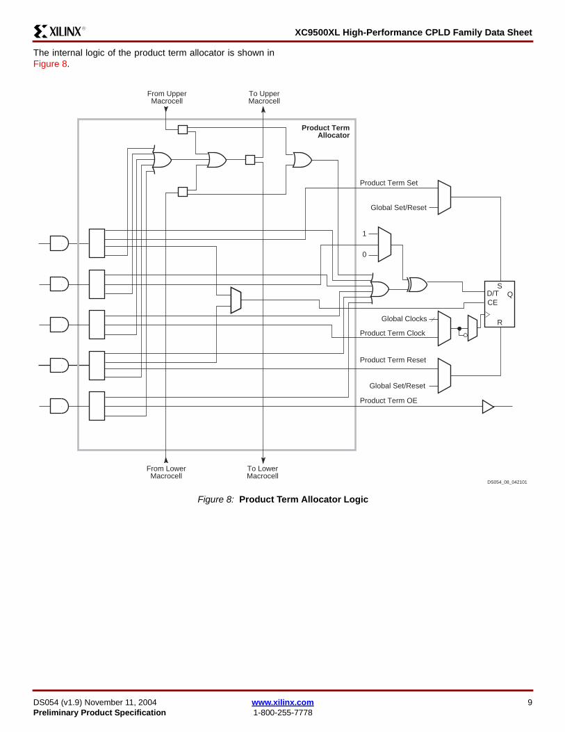
XC9500XL High-Performance CPLD Family Data SheetR
The internal logic of the product term allocator is shown inFigure 8
Figure 8 Product Term Allocator Logic
DT QS
R
From UpperMacrocell
To UpperMacrocell
Product Term Set
Product Term Clock
Product Term Reset
Global SetReset
Global SetReset
Global Clocks
Product Term OE
Product TermAllocator
To LowerMacrocell
From LowerMacrocell
DS054_08_042101
1
0
CE
DS054 (v19) November 11 2004 wwwxilinxcom 9Preliminary Product Specification 1-800-255-7778
XC9500XL High-Performance CPLD Family Data Sheet R
FastCONNECT II Switch MatrixThe FastCONNECT II Switch Matrix connects signals to theFB inputs as shown in Figure 9 All IOB outputs (corre-
sponding to user pin inputs) and all FB outputs drive theFastCONNECT II matrix Any of these (up to a fan-in limit of54) may be selected to drive each FB with a uniform delay
Figure 9 FastCONNECT II Switch Matrix
DS054_09_042101
Function Block
FastCONNECT IISwitch Matrix
(54)
IO
Function Block
IO Block
18
18
IO Block
(54)
IO
DT Q
DT Q
10 wwwxilinxcom DS054 (v19) November 11 20041-800-255-7778 Preliminary Product Specification
XC9500XL High-Performance CPLD Family Data SheetR
IO BlockThe IO Block (IOB) interfaces between the internal logicand the device user IO pins Each IOB includes an input
buffer output driver output enable selection multiplexerand user programmable ground control See Figure 10 fordetails
The input buffer is compatible with 5V CMOS 5V TTL 33VCMOS and 25V CMOS signals The input buffer uses theinternal 33V voltage supply (VCCINT) to ensure that theinput thresholds are constant and do not vary with the VCCIOvoltage Each input buffer provides input hysteresis (50 mV
typical) to help reduce system noise for input signals withslow rise or fall edges
Each output driver is designed to provide fast switching withminimal power noise All output drivers in the device may be
Figure 10 IO Block and Output Enable Capability
IO Block
Macrocell
DS054_10_042101
Product Term OE PTOE
Switch Matrix
OUT
(Inversion inAND-array)
Global OE 1
1
To otherMacrocells
Slew RateControl
0
Global OE 2
Available in XC95144XLand XC95288XLGlobal OE 3
Global OE 4
IOGTS1
IO
IOGTS2
IOGTS3
IOGTS4
To FastCONNECT
User-Programmable
Ground
Bus-Hold
DS054 (v19) November 11 2004 wwwxilinxcom 11Preliminary Product Specification 1-800-255-7778
XC9500XL High-Performance CPLD Family Data Sheet R
configured for driving either 33V CMOS levels (which arecompatible with 5V TTL levels as well) or 25V CMOS levelsby connecting the device output voltage supply (VCCIO) to a33V or 25V voltage supply Figure 11 shows how theXC9500XL device can be used in 33V only systems andmixed voltage systems with any combination of 5V 33Vand 25V power supplies
Each output driver can also be configured for slew-rate lim-ited operation Output edge rates may be slowed down toreduce system noise (with an additional time delay of tSLEW)under user control See Figure 12
The output enable may be generated from one of fouroptions a product term signal from the macrocell any of theglobal output enable signals (GTS) always ldquo1rdquo or alwaysldquo0rdquo There are two global output enables for devices with 72or fewer macrocells and four global output enables fordevices with 144 or more macrocells Any selected outputenable signal may be inverted locally at each pin output toprovide maximal design flexibility
Each IOB provides user programmable ground pin capabil-ity This allows device IO pins to be configured as additionalground pins in order to force otherwise unused pins to a lowvoltage state as well as provide for additional device
grounding capability This grounding of the pin is achievedby internal logic that forces a logic low output regardless ofthe internal macrocell signal so the internal macrocell logicis unaffected by the programmable ground pin capability
Each IOB also provides for bus-hold circuitry (also called aldquokeeperrdquo)that is active during valid user operation Thebus-hold feature eliminates the need to tie unused pinseither high or low by holding the last known state of the inputuntil the next input signal is present The bus-hold circuitdrives back the same state via a nominal resistance (RBH)of 50k ohms See Figure 13 Note the bus-hold output willdrive no higher than VCCIO to prevent overdriving signalswhen interfacing to 25V components
When the device is not in valid user operation the bus-holdcircuit defaults to an equivalent 50k ohm pull-up resistor inorder to provide a known repeatable device state Thisoccurs when the device is in the erased state in program-ming mode in JTAG INTEST mode or during initialpower-up A pull-down resistor (1k ohm) may be externallyadded to any pin to override the default RBH resistance toforce a low state during power-up or any of these othermodes
5V Tolerant IOsThe IOs on each XC9500XL device are fully 5V toleranteven though the core power supply is 33 volts This allows5V CMOS signals to connect directly to the XC9500XLinputs without damage In addition the 33V VCCINT powersupply can be applied before or after 5V signals are appliedto the IOs In mixed 5V33V25V systems the user pinsthe core power supply (VCCINT) and the output power sup-ply (VCCIO) may have power applied in any order Thismakes the XC9500XL devices immune to power supplysequencing problems
Xilinx proprietary ESD circuitry and high impedance initialstate permit hot plugging cards using these devices
Pin-Locking CapabilityThe capability to lock the user defined pin assignments dur-ing design iteration depends on the ability of the architec-ture to adapt to unexpected changes The XC9500XLdevices incorporate architectural features that enhance theability to accept design changes while maintaining the samepinout
Figure 11 XC9500XL Devices in (a) 33V only and (b) Mixed 5V33V25V Systems
IN OUT
25V33V
GND
(b)
25V CMOS
IN OUT
XC9500XLCPLD
XC9500XLCPLD
VCCINT VCCIO VCCINT VCCIO
33V
GND
(a)
33V
0V
5V
0V
33V
0V
25V
0V
25V
0V
33V CMOS 5V TTL
DS054_11_042101
25V CMOS
33V CMOS or
5V TTL or
5V
0V
5V CMOS
5V
0V
33V
0V
25V
0V
25V CMOS
33V CMOS or
5V TTL or
5V
0V
5V CMOS
12 wwwxilinxcom DS054 (v19) November 11 20041-800-255-7778 Preliminary Product Specification
XC9500XL High-Performance CPLD Family Data SheetR
The XC9500XL architecture provides for superior pin-lock-ing characteristics with a combination of large number ofrouting switches in the FastCONNECT II switch matrix a54-wide input Function Block and flexible bi-directionalproduct term allocation within each macrocell These fea-tures address design changes that require adding or chang-ing internal routing including additional signals into existingequations or increasing equation complexity respectively
For extensive design changes requiring higher logic capac-ity than is available in the initially chosen device the newdesign may be able to fit into a larger pin-compatible deviceusing the same pin assignments The same board may beused with a higher density device without the expense ofboard rework
In-System ProgrammingOne or more XC9500XL devices can be daisy chainedtogether and programmed in-system via a standard 4-pinJTAG protocol as shown in Figure 14 In-system program-ming offers quick and efficient design iterations and elimi-nates package handling The Xilinx development systemprovides the programming data sequence using a Xilinxdownload cable a third-party JTAG development systemJTAG-compatible board tester or a simple microprocessorinterface that emulates the JTAG instruction sequence
All IOs are 3-stated and pulled high by the bus-hold cir-cuitry during in-system programming If a particular signalmust remain low during this time then a pulldown resistormay be added to the pin
External ProgrammingXC9500XL devices can also be programmed by the XilinxHW-130 device programmer as well as third-party program-mers This provides the added flexibility of using pre-pro-grammed devices during manufacturing with an in-systemprogrammable option for future enhancements and designchanges
Reliability and EnduranceAll XC9500XL CPLDs provide a minimum endurance levelof 10000 in-system programerase cycles and a minimumdata retention of 20 years Each device meets all functionalperformance and data retention specifications within thisendurance limit
IEEE 11491 Boundary-Scan (JTAG)XC9500XL devices fully support IEEE 11491 bound-ary-scan (JTAG) EXTEST SAMPLEPRELOAD BYPASSUSERCODE INTEST IDCODE HIGHZ and CLAMPinstructions are supported in each device Additionalinstructions are included for in-system programming opera-tions
Figure 12 Output Slew-Rate Control For (a) Rising and (b) Falling Outputs
Time0 0
15V
Standard
OutputVoltage
(a)
Slew-Rate Limited
Time
OutputVoltage
(b)
Standard
Slew-Rate Limited
VCCIO
TSLEW TSLEW
15V
DS054_12_042101
Figure 13 Bus-Hold Logic
RBH
IO
Set to PINduring valid useroperation Drive to
VCCIO Level
PIN
0
DS054_13_042101
DS054 (v19) November 11 2004 wwwxilinxcom 13Preliminary Product Specification 1-800-255-7778
XC9500XL High-Performance CPLD Family Data Sheet R
Design SecurityXC9500XL devices incorporate advanced data security fea-tures which fully protect the programming data againstunauthorized reading or inadvertent device erasurerepro-gramming Table 3 shows the four different security settingsavailable
The read security bits can be set by the user to prevent theinternal programming pattern from being read or copiedWhen set they also inhibit further program operations butallow device erase Erasing the entire device is the only wayto reset the read security bit
The write security bits provide added protection againstaccidental device erasure or reprogramming when theJTAG pins are subject to noise such as during systempower-up Once set the write-protection may be deacti-
vated when the device needs to be reprogrammed with avalid pattern with a specific sequence of JTAG instructions
Low Power Mode All XC9500XL devices offer a low-power mode for individualmacrocells or across all macrocells This feature allows thedevice power to be significantly reduced
Each individual macrocell may be programmed inlow-power mode by the user Performance-critical parts ofthe application can remain in standard power mode whileother parts of the application may be programmed forlow-power operation to reduce the overall power dissipa-tion Macrocells programmed for low-power mode incuradditional delay (tLP) in pin-to-pin combinatorial delay aswell as register setup time Product term clock to output andproduct term output enable delays are unaffected by themacrocell power-setting Signals switching at rates lessthan 50 ns risefall time should be assigned to the macro-cells configured in low power mode
Timing ModelThe uniformity of the XC9500XL architecture allows a sim-plified timing model for the entire device The basic timingmodel shown in Figure 15 is valid for macrocell functionsthat use the direct product terms only with standard powersetting and standard slew rate setting Table 4 shows howeach of the key timing parameters is affected by the productterm allocator (if needed) low-power setting and slew-lim-ited setting
The product term allocation time depends on the logic spanof the macrocell function which is defined as one less thanthe maximum number of allocators in the product term pathIf only direct product terms are used then the logic span is0 The example in Figure 6 shows that up to 15 productterms are available with a span of 1 In the case of Figure 7the 18 product term function has a span of 2
Table 3 Data Security Options
Read Security
Default Set
Writ
e Se
curit
y DefaultRead AllowedProgramErase
Allowed
Read InhibitedProgram Inhibited
Erase Allowed
SetRead AllowedProgramErase
Allowed
Read InhibitedProgramErase
Inhibited
Figure 14 System Programming Operation (a) Solder Device to PCB and (b) Program Using Download Cable
X5902
GND
V CC
(a) (b)
14 wwwxilinxcom DS054 (v19) November 11 20041-800-255-7778 Preliminary Product Specification
XC9500XL High-Performance CPLD Family Data SheetR
Detailed timing information may be derived from the full tim-ing model shown in Figure 16 The values and explanations
for each parameter are given in the individual device datasheets
Figure 15 Basic Timing Model
Figure 16 Detailed Timing Model
CombinatorialLogic
Propagation Delay = TPD(a)
CombinatorialLogic
Setup Time = TSU
TCO
TPSU
TPCO
Clock to Out Time = TCO(b)
DT Q
CombinatorialLogic
Internal System Cycle Time = TSYSTEM
DS054_15_042101
(d)
DT Q
CombinatorialLogic
Setup Time = TPSU Clock to Out Time = TPCO(c)
P-Term ClockPath
DT Q
DT Q
SR
TIN
TLOGILP STPTA
TF
TPDI
TSUI TCOITHI
TAOITRAI
TOUT
TSLEW
TEN
DS054_16_042101
TLOGI
TPTCK
TPTSR
TPTTS
TGCK
TGSR
TGTS
Macrocell
CE
DS054 (v19) November 11 2004 wwwxilinxcom 15Preliminary Product Specification 1-800-255-7778
XC9500XL High-Performance CPLD Family Data Sheet R
Power-Up CharacteristicsThe XC9500XL devices are well behaved under all operat-ing conditions During power-up each XC9500XL deviceemploys internal circuitry which keeps the device in the qui-escent state until the VCCINT supply voltage is at a safe level(approximately 25V) During this time all device pins andJTAG pins are disabled and all device outputs are disabledwith the pins weakly pulled high as shown in Table 5 Whenthe supply voltage reaches a safe level all user registersbecome initialized (typically within 200 micros) and the deviceis immediately available for operation as shown inFigure 17
If the device is in the erased state (before any user patternis programmed) the device outputs remain disabled withweak pull-up The JTAG pins are enabled to allow thedevice to be programmed at any time All devices areshipped in the erased state from the factory
If the device is programmed the device inputs and outputstake on their configured states for normal operation TheJTAG pins are enabled to allow device erasure or bound-ary-scan tests at any time
Development System SupportThe XC9500XL family and associated in-system program-ming capabilities are fully supported in either software solu-tions available from Xilinx
The Foundation Series is an all-in-one development systemcontaining schematic entry HDL (VHDL Verilog and
ABEL) and simulation capabilities It supports theXC9500XL family as well as other CPLD and FPGA fami-lies
The Alliance Series includes CPLD and FPGA implementa-tion technology as well as all necessary libraries and inter-faces for Alliance partner EDA solutions
FastFLASH TechnologyAn advanced 035 micron feature size CMOS Flash process isused to fabricate all XC9500XL devices The FastFLASH pro-cess provides high performance logic capability fast pro-gramming times and superior reliability and enduranceratings
Figure 17 Device Behavior During Power-up
VCCINT
NoPower
38 V(Typ)
0VNo
PowerQuiescent
StateQuiescent
StateUser Operation
Initialization of User Registers
DS054_17_042101
25V(Typ)
Table 4 Timing Model Parameters
Parameter DescriptionProduct TermAllocator(1)
MacrocellLow-Power Setting
Output Slew-Limited
SettingTPD Propagation Delay + TPTA S + TLP + TSLEWTSU Global Clock Setup Time + TPTA S + TLP ndashTCO Global Clock-to-output - - + TSLEWTPSU Product Term Clock Setup Time + TPTA S + TLP -TPCO Product Term Clock-to-output - - + TSLEW
TSYSTEM Internal System Cycle Period + TPTA S + TLP -Notes 1 S = the logic span of the function as defined in the text
Table 5 XC9500XL Device CharacteristicsDevice Circuitry Quiescent State Erased Device Operation Valid User Operation
IOB Bus-Hold Pull-up Pull-up Bus-HoldDevice Outputs Disabled Disabled As ConfiguredDevice Inputs and Clocks Disabled Disabled As ConfiguredFunction Block Disabled Disabled As ConfiguredJTAG Controller Disabled Enabled Enabled
16 wwwxilinxcom DS054 (v19) November 11 20041-800-255-7778 Preliminary Product Specification
XC9500XL High-Performance CPLD Family Data SheetR
Further ReadingThe following Xilinx links go to relevant XC9500XL CPLDdocumentation
Data Sheets Application Notes and White PapersPackagingOnline Store
Revision HistoryThe following table shows the revision history for this document
Date Version Revision
092898 10 Initial Xilinx release
100298 11 Figure 1 correction
020399 12 Included hot socket reference revised layout BGA package change for XC95288XL
040299 13 Minor typesetting corrections
060799 14 Minor typesetting corrections
060799 15 Added CS280 package
012502 16 Added DS054 data sheet number Added 44-pin VQFP package Updated Device Family table
020703 17 Added Further Reading section
080204 18 Added Pb-free documentation
111104 19 Changes to package designations in Table 2 on page 2
DS054 (v19) November 11 2004 wwwxilinxcom 17Preliminary Product Specification 1-800-255-7778
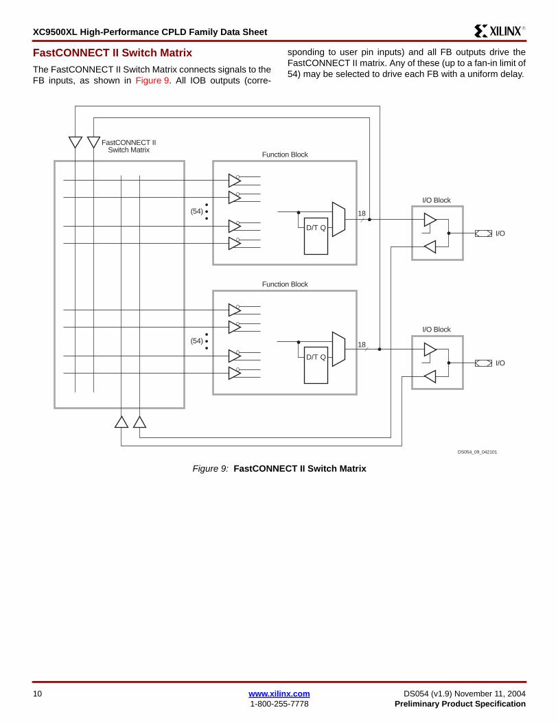
XC9500XL High-Performance CPLD Family Data Sheet R
FastCONNECT II Switch MatrixThe FastCONNECT II Switch Matrix connects signals to theFB inputs as shown in Figure 9 All IOB outputs (corre-
sponding to user pin inputs) and all FB outputs drive theFastCONNECT II matrix Any of these (up to a fan-in limit of54) may be selected to drive each FB with a uniform delay
Figure 9 FastCONNECT II Switch Matrix
DS054_09_042101
Function Block
FastCONNECT IISwitch Matrix
(54)
IO
Function Block
IO Block
18
18
IO Block
(54)
IO
DT Q
DT Q
10 wwwxilinxcom DS054 (v19) November 11 20041-800-255-7778 Preliminary Product Specification
XC9500XL High-Performance CPLD Family Data SheetR
IO BlockThe IO Block (IOB) interfaces between the internal logicand the device user IO pins Each IOB includes an input
buffer output driver output enable selection multiplexerand user programmable ground control See Figure 10 fordetails
The input buffer is compatible with 5V CMOS 5V TTL 33VCMOS and 25V CMOS signals The input buffer uses theinternal 33V voltage supply (VCCINT) to ensure that theinput thresholds are constant and do not vary with the VCCIOvoltage Each input buffer provides input hysteresis (50 mV
typical) to help reduce system noise for input signals withslow rise or fall edges
Each output driver is designed to provide fast switching withminimal power noise All output drivers in the device may be
Figure 10 IO Block and Output Enable Capability
IO Block
Macrocell
DS054_10_042101
Product Term OE PTOE
Switch Matrix
OUT
(Inversion inAND-array)
Global OE 1
1
To otherMacrocells
Slew RateControl
0
Global OE 2
Available in XC95144XLand XC95288XLGlobal OE 3
Global OE 4
IOGTS1
IO
IOGTS2
IOGTS3
IOGTS4
To FastCONNECT
User-Programmable
Ground
Bus-Hold
DS054 (v19) November 11 2004 wwwxilinxcom 11Preliminary Product Specification 1-800-255-7778
XC9500XL High-Performance CPLD Family Data Sheet R
configured for driving either 33V CMOS levels (which arecompatible with 5V TTL levels as well) or 25V CMOS levelsby connecting the device output voltage supply (VCCIO) to a33V or 25V voltage supply Figure 11 shows how theXC9500XL device can be used in 33V only systems andmixed voltage systems with any combination of 5V 33Vand 25V power supplies
Each output driver can also be configured for slew-rate lim-ited operation Output edge rates may be slowed down toreduce system noise (with an additional time delay of tSLEW)under user control See Figure 12
The output enable may be generated from one of fouroptions a product term signal from the macrocell any of theglobal output enable signals (GTS) always ldquo1rdquo or alwaysldquo0rdquo There are two global output enables for devices with 72or fewer macrocells and four global output enables fordevices with 144 or more macrocells Any selected outputenable signal may be inverted locally at each pin output toprovide maximal design flexibility
Each IOB provides user programmable ground pin capabil-ity This allows device IO pins to be configured as additionalground pins in order to force otherwise unused pins to a lowvoltage state as well as provide for additional device
grounding capability This grounding of the pin is achievedby internal logic that forces a logic low output regardless ofthe internal macrocell signal so the internal macrocell logicis unaffected by the programmable ground pin capability
Each IOB also provides for bus-hold circuitry (also called aldquokeeperrdquo)that is active during valid user operation Thebus-hold feature eliminates the need to tie unused pinseither high or low by holding the last known state of the inputuntil the next input signal is present The bus-hold circuitdrives back the same state via a nominal resistance (RBH)of 50k ohms See Figure 13 Note the bus-hold output willdrive no higher than VCCIO to prevent overdriving signalswhen interfacing to 25V components
When the device is not in valid user operation the bus-holdcircuit defaults to an equivalent 50k ohm pull-up resistor inorder to provide a known repeatable device state Thisoccurs when the device is in the erased state in program-ming mode in JTAG INTEST mode or during initialpower-up A pull-down resistor (1k ohm) may be externallyadded to any pin to override the default RBH resistance toforce a low state during power-up or any of these othermodes
5V Tolerant IOsThe IOs on each XC9500XL device are fully 5V toleranteven though the core power supply is 33 volts This allows5V CMOS signals to connect directly to the XC9500XLinputs without damage In addition the 33V VCCINT powersupply can be applied before or after 5V signals are appliedto the IOs In mixed 5V33V25V systems the user pinsthe core power supply (VCCINT) and the output power sup-ply (VCCIO) may have power applied in any order Thismakes the XC9500XL devices immune to power supplysequencing problems
Xilinx proprietary ESD circuitry and high impedance initialstate permit hot plugging cards using these devices
Pin-Locking CapabilityThe capability to lock the user defined pin assignments dur-ing design iteration depends on the ability of the architec-ture to adapt to unexpected changes The XC9500XLdevices incorporate architectural features that enhance theability to accept design changes while maintaining the samepinout
Figure 11 XC9500XL Devices in (a) 33V only and (b) Mixed 5V33V25V Systems
IN OUT
25V33V
GND
(b)
25V CMOS
IN OUT
XC9500XLCPLD
XC9500XLCPLD
VCCINT VCCIO VCCINT VCCIO
33V
GND
(a)
33V
0V
5V
0V
33V
0V
25V
0V
25V
0V
33V CMOS 5V TTL
DS054_11_042101
25V CMOS
33V CMOS or
5V TTL or
5V
0V
5V CMOS
5V
0V
33V
0V
25V
0V
25V CMOS
33V CMOS or
5V TTL or
5V
0V
5V CMOS
12 wwwxilinxcom DS054 (v19) November 11 20041-800-255-7778 Preliminary Product Specification
XC9500XL High-Performance CPLD Family Data SheetR
The XC9500XL architecture provides for superior pin-lock-ing characteristics with a combination of large number ofrouting switches in the FastCONNECT II switch matrix a54-wide input Function Block and flexible bi-directionalproduct term allocation within each macrocell These fea-tures address design changes that require adding or chang-ing internal routing including additional signals into existingequations or increasing equation complexity respectively
For extensive design changes requiring higher logic capac-ity than is available in the initially chosen device the newdesign may be able to fit into a larger pin-compatible deviceusing the same pin assignments The same board may beused with a higher density device without the expense ofboard rework
In-System ProgrammingOne or more XC9500XL devices can be daisy chainedtogether and programmed in-system via a standard 4-pinJTAG protocol as shown in Figure 14 In-system program-ming offers quick and efficient design iterations and elimi-nates package handling The Xilinx development systemprovides the programming data sequence using a Xilinxdownload cable a third-party JTAG development systemJTAG-compatible board tester or a simple microprocessorinterface that emulates the JTAG instruction sequence
All IOs are 3-stated and pulled high by the bus-hold cir-cuitry during in-system programming If a particular signalmust remain low during this time then a pulldown resistormay be added to the pin
External ProgrammingXC9500XL devices can also be programmed by the XilinxHW-130 device programmer as well as third-party program-mers This provides the added flexibility of using pre-pro-grammed devices during manufacturing with an in-systemprogrammable option for future enhancements and designchanges
Reliability and EnduranceAll XC9500XL CPLDs provide a minimum endurance levelof 10000 in-system programerase cycles and a minimumdata retention of 20 years Each device meets all functionalperformance and data retention specifications within thisendurance limit
IEEE 11491 Boundary-Scan (JTAG)XC9500XL devices fully support IEEE 11491 bound-ary-scan (JTAG) EXTEST SAMPLEPRELOAD BYPASSUSERCODE INTEST IDCODE HIGHZ and CLAMPinstructions are supported in each device Additionalinstructions are included for in-system programming opera-tions
Figure 12 Output Slew-Rate Control For (a) Rising and (b) Falling Outputs
Time0 0
15V
Standard
OutputVoltage
(a)
Slew-Rate Limited
Time
OutputVoltage
(b)
Standard
Slew-Rate Limited
VCCIO
TSLEW TSLEW
15V
DS054_12_042101
Figure 13 Bus-Hold Logic
RBH
IO
Set to PINduring valid useroperation Drive to
VCCIO Level
PIN
0
DS054_13_042101
DS054 (v19) November 11 2004 wwwxilinxcom 13Preliminary Product Specification 1-800-255-7778
XC9500XL High-Performance CPLD Family Data Sheet R
Design SecurityXC9500XL devices incorporate advanced data security fea-tures which fully protect the programming data againstunauthorized reading or inadvertent device erasurerepro-gramming Table 3 shows the four different security settingsavailable
The read security bits can be set by the user to prevent theinternal programming pattern from being read or copiedWhen set they also inhibit further program operations butallow device erase Erasing the entire device is the only wayto reset the read security bit
The write security bits provide added protection againstaccidental device erasure or reprogramming when theJTAG pins are subject to noise such as during systempower-up Once set the write-protection may be deacti-
vated when the device needs to be reprogrammed with avalid pattern with a specific sequence of JTAG instructions
Low Power Mode All XC9500XL devices offer a low-power mode for individualmacrocells or across all macrocells This feature allows thedevice power to be significantly reduced
Each individual macrocell may be programmed inlow-power mode by the user Performance-critical parts ofthe application can remain in standard power mode whileother parts of the application may be programmed forlow-power operation to reduce the overall power dissipa-tion Macrocells programmed for low-power mode incuradditional delay (tLP) in pin-to-pin combinatorial delay aswell as register setup time Product term clock to output andproduct term output enable delays are unaffected by themacrocell power-setting Signals switching at rates lessthan 50 ns risefall time should be assigned to the macro-cells configured in low power mode
Timing ModelThe uniformity of the XC9500XL architecture allows a sim-plified timing model for the entire device The basic timingmodel shown in Figure 15 is valid for macrocell functionsthat use the direct product terms only with standard powersetting and standard slew rate setting Table 4 shows howeach of the key timing parameters is affected by the productterm allocator (if needed) low-power setting and slew-lim-ited setting
The product term allocation time depends on the logic spanof the macrocell function which is defined as one less thanthe maximum number of allocators in the product term pathIf only direct product terms are used then the logic span is0 The example in Figure 6 shows that up to 15 productterms are available with a span of 1 In the case of Figure 7the 18 product term function has a span of 2
Table 3 Data Security Options
Read Security
Default Set
Writ
e Se
curit
y DefaultRead AllowedProgramErase
Allowed
Read InhibitedProgram Inhibited
Erase Allowed
SetRead AllowedProgramErase
Allowed
Read InhibitedProgramErase
Inhibited
Figure 14 System Programming Operation (a) Solder Device to PCB and (b) Program Using Download Cable
X5902
GND
V CC
(a) (b)
14 wwwxilinxcom DS054 (v19) November 11 20041-800-255-7778 Preliminary Product Specification
XC9500XL High-Performance CPLD Family Data SheetR
Detailed timing information may be derived from the full tim-ing model shown in Figure 16 The values and explanations
for each parameter are given in the individual device datasheets
Figure 15 Basic Timing Model
Figure 16 Detailed Timing Model
CombinatorialLogic
Propagation Delay = TPD(a)
CombinatorialLogic
Setup Time = TSU
TCO
TPSU
TPCO
Clock to Out Time = TCO(b)
DT Q
CombinatorialLogic
Internal System Cycle Time = TSYSTEM
DS054_15_042101
(d)
DT Q
CombinatorialLogic
Setup Time = TPSU Clock to Out Time = TPCO(c)
P-Term ClockPath
DT Q
DT Q
SR
TIN
TLOGILP STPTA
TF
TPDI
TSUI TCOITHI
TAOITRAI
TOUT
TSLEW
TEN
DS054_16_042101
TLOGI
TPTCK
TPTSR
TPTTS
TGCK
TGSR
TGTS
Macrocell
CE
DS054 (v19) November 11 2004 wwwxilinxcom 15Preliminary Product Specification 1-800-255-7778
XC9500XL High-Performance CPLD Family Data Sheet R
Power-Up CharacteristicsThe XC9500XL devices are well behaved under all operat-ing conditions During power-up each XC9500XL deviceemploys internal circuitry which keeps the device in the qui-escent state until the VCCINT supply voltage is at a safe level(approximately 25V) During this time all device pins andJTAG pins are disabled and all device outputs are disabledwith the pins weakly pulled high as shown in Table 5 Whenthe supply voltage reaches a safe level all user registersbecome initialized (typically within 200 micros) and the deviceis immediately available for operation as shown inFigure 17
If the device is in the erased state (before any user patternis programmed) the device outputs remain disabled withweak pull-up The JTAG pins are enabled to allow thedevice to be programmed at any time All devices areshipped in the erased state from the factory
If the device is programmed the device inputs and outputstake on their configured states for normal operation TheJTAG pins are enabled to allow device erasure or bound-ary-scan tests at any time
Development System SupportThe XC9500XL family and associated in-system program-ming capabilities are fully supported in either software solu-tions available from Xilinx
The Foundation Series is an all-in-one development systemcontaining schematic entry HDL (VHDL Verilog and
ABEL) and simulation capabilities It supports theXC9500XL family as well as other CPLD and FPGA fami-lies
The Alliance Series includes CPLD and FPGA implementa-tion technology as well as all necessary libraries and inter-faces for Alliance partner EDA solutions
FastFLASH TechnologyAn advanced 035 micron feature size CMOS Flash process isused to fabricate all XC9500XL devices The FastFLASH pro-cess provides high performance logic capability fast pro-gramming times and superior reliability and enduranceratings
Figure 17 Device Behavior During Power-up
VCCINT
NoPower
38 V(Typ)
0VNo
PowerQuiescent
StateQuiescent
StateUser Operation
Initialization of User Registers
DS054_17_042101
25V(Typ)
Table 4 Timing Model Parameters
Parameter DescriptionProduct TermAllocator(1)
MacrocellLow-Power Setting
Output Slew-Limited
SettingTPD Propagation Delay + TPTA S + TLP + TSLEWTSU Global Clock Setup Time + TPTA S + TLP ndashTCO Global Clock-to-output - - + TSLEWTPSU Product Term Clock Setup Time + TPTA S + TLP -TPCO Product Term Clock-to-output - - + TSLEW
TSYSTEM Internal System Cycle Period + TPTA S + TLP -Notes 1 S = the logic span of the function as defined in the text
Table 5 XC9500XL Device CharacteristicsDevice Circuitry Quiescent State Erased Device Operation Valid User Operation
IOB Bus-Hold Pull-up Pull-up Bus-HoldDevice Outputs Disabled Disabled As ConfiguredDevice Inputs and Clocks Disabled Disabled As ConfiguredFunction Block Disabled Disabled As ConfiguredJTAG Controller Disabled Enabled Enabled
16 wwwxilinxcom DS054 (v19) November 11 20041-800-255-7778 Preliminary Product Specification
XC9500XL High-Performance CPLD Family Data SheetR
Further ReadingThe following Xilinx links go to relevant XC9500XL CPLDdocumentation
Data Sheets Application Notes and White PapersPackagingOnline Store
Revision HistoryThe following table shows the revision history for this document
Date Version Revision
092898 10 Initial Xilinx release
100298 11 Figure 1 correction
020399 12 Included hot socket reference revised layout BGA package change for XC95288XL
040299 13 Minor typesetting corrections
060799 14 Minor typesetting corrections
060799 15 Added CS280 package
012502 16 Added DS054 data sheet number Added 44-pin VQFP package Updated Device Family table
020703 17 Added Further Reading section
080204 18 Added Pb-free documentation
111104 19 Changes to package designations in Table 2 on page 2
DS054 (v19) November 11 2004 wwwxilinxcom 17Preliminary Product Specification 1-800-255-7778
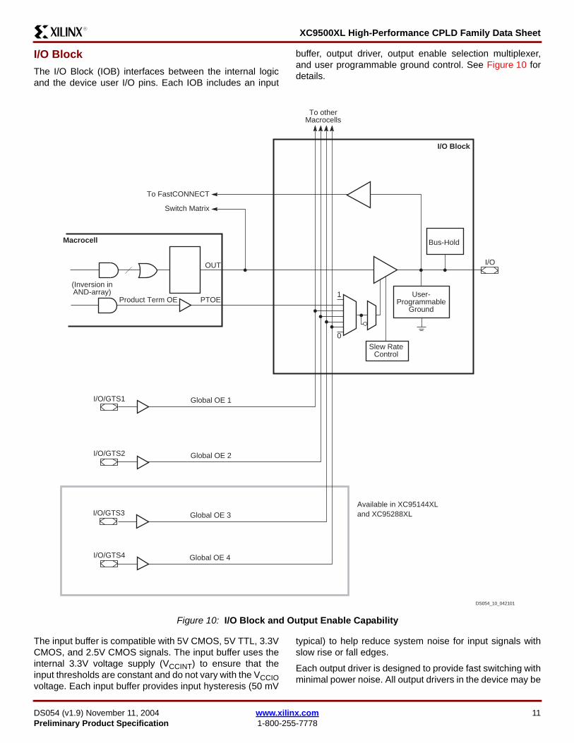
XC9500XL High-Performance CPLD Family Data SheetR
IO BlockThe IO Block (IOB) interfaces between the internal logicand the device user IO pins Each IOB includes an input
buffer output driver output enable selection multiplexerand user programmable ground control See Figure 10 fordetails
The input buffer is compatible with 5V CMOS 5V TTL 33VCMOS and 25V CMOS signals The input buffer uses theinternal 33V voltage supply (VCCINT) to ensure that theinput thresholds are constant and do not vary with the VCCIOvoltage Each input buffer provides input hysteresis (50 mV
typical) to help reduce system noise for input signals withslow rise or fall edges
Each output driver is designed to provide fast switching withminimal power noise All output drivers in the device may be
Figure 10 IO Block and Output Enable Capability
IO Block
Macrocell
DS054_10_042101
Product Term OE PTOE
Switch Matrix
OUT
(Inversion inAND-array)
Global OE 1
1
To otherMacrocells
Slew RateControl
0
Global OE 2
Available in XC95144XLand XC95288XLGlobal OE 3
Global OE 4
IOGTS1
IO
IOGTS2
IOGTS3
IOGTS4
To FastCONNECT
User-Programmable
Ground
Bus-Hold
DS054 (v19) November 11 2004 wwwxilinxcom 11Preliminary Product Specification 1-800-255-7778
XC9500XL High-Performance CPLD Family Data Sheet R
configured for driving either 33V CMOS levels (which arecompatible with 5V TTL levels as well) or 25V CMOS levelsby connecting the device output voltage supply (VCCIO) to a33V or 25V voltage supply Figure 11 shows how theXC9500XL device can be used in 33V only systems andmixed voltage systems with any combination of 5V 33Vand 25V power supplies
Each output driver can also be configured for slew-rate lim-ited operation Output edge rates may be slowed down toreduce system noise (with an additional time delay of tSLEW)under user control See Figure 12
The output enable may be generated from one of fouroptions a product term signal from the macrocell any of theglobal output enable signals (GTS) always ldquo1rdquo or alwaysldquo0rdquo There are two global output enables for devices with 72or fewer macrocells and four global output enables fordevices with 144 or more macrocells Any selected outputenable signal may be inverted locally at each pin output toprovide maximal design flexibility
Each IOB provides user programmable ground pin capabil-ity This allows device IO pins to be configured as additionalground pins in order to force otherwise unused pins to a lowvoltage state as well as provide for additional device
grounding capability This grounding of the pin is achievedby internal logic that forces a logic low output regardless ofthe internal macrocell signal so the internal macrocell logicis unaffected by the programmable ground pin capability
Each IOB also provides for bus-hold circuitry (also called aldquokeeperrdquo)that is active during valid user operation Thebus-hold feature eliminates the need to tie unused pinseither high or low by holding the last known state of the inputuntil the next input signal is present The bus-hold circuitdrives back the same state via a nominal resistance (RBH)of 50k ohms See Figure 13 Note the bus-hold output willdrive no higher than VCCIO to prevent overdriving signalswhen interfacing to 25V components
When the device is not in valid user operation the bus-holdcircuit defaults to an equivalent 50k ohm pull-up resistor inorder to provide a known repeatable device state Thisoccurs when the device is in the erased state in program-ming mode in JTAG INTEST mode or during initialpower-up A pull-down resistor (1k ohm) may be externallyadded to any pin to override the default RBH resistance toforce a low state during power-up or any of these othermodes
5V Tolerant IOsThe IOs on each XC9500XL device are fully 5V toleranteven though the core power supply is 33 volts This allows5V CMOS signals to connect directly to the XC9500XLinputs without damage In addition the 33V VCCINT powersupply can be applied before or after 5V signals are appliedto the IOs In mixed 5V33V25V systems the user pinsthe core power supply (VCCINT) and the output power sup-ply (VCCIO) may have power applied in any order Thismakes the XC9500XL devices immune to power supplysequencing problems
Xilinx proprietary ESD circuitry and high impedance initialstate permit hot plugging cards using these devices
Pin-Locking CapabilityThe capability to lock the user defined pin assignments dur-ing design iteration depends on the ability of the architec-ture to adapt to unexpected changes The XC9500XLdevices incorporate architectural features that enhance theability to accept design changes while maintaining the samepinout
Figure 11 XC9500XL Devices in (a) 33V only and (b) Mixed 5V33V25V Systems
IN OUT
25V33V
GND
(b)
25V CMOS
IN OUT
XC9500XLCPLD
XC9500XLCPLD
VCCINT VCCIO VCCINT VCCIO
33V
GND
(a)
33V
0V
5V
0V
33V
0V
25V
0V
25V
0V
33V CMOS 5V TTL
DS054_11_042101
25V CMOS
33V CMOS or
5V TTL or
5V
0V
5V CMOS
5V
0V
33V
0V
25V
0V
25V CMOS
33V CMOS or
5V TTL or
5V
0V
5V CMOS
12 wwwxilinxcom DS054 (v19) November 11 20041-800-255-7778 Preliminary Product Specification
XC9500XL High-Performance CPLD Family Data SheetR
The XC9500XL architecture provides for superior pin-lock-ing characteristics with a combination of large number ofrouting switches in the FastCONNECT II switch matrix a54-wide input Function Block and flexible bi-directionalproduct term allocation within each macrocell These fea-tures address design changes that require adding or chang-ing internal routing including additional signals into existingequations or increasing equation complexity respectively
For extensive design changes requiring higher logic capac-ity than is available in the initially chosen device the newdesign may be able to fit into a larger pin-compatible deviceusing the same pin assignments The same board may beused with a higher density device without the expense ofboard rework
In-System ProgrammingOne or more XC9500XL devices can be daisy chainedtogether and programmed in-system via a standard 4-pinJTAG protocol as shown in Figure 14 In-system program-ming offers quick and efficient design iterations and elimi-nates package handling The Xilinx development systemprovides the programming data sequence using a Xilinxdownload cable a third-party JTAG development systemJTAG-compatible board tester or a simple microprocessorinterface that emulates the JTAG instruction sequence
All IOs are 3-stated and pulled high by the bus-hold cir-cuitry during in-system programming If a particular signalmust remain low during this time then a pulldown resistormay be added to the pin
External ProgrammingXC9500XL devices can also be programmed by the XilinxHW-130 device programmer as well as third-party program-mers This provides the added flexibility of using pre-pro-grammed devices during manufacturing with an in-systemprogrammable option for future enhancements and designchanges
Reliability and EnduranceAll XC9500XL CPLDs provide a minimum endurance levelof 10000 in-system programerase cycles and a minimumdata retention of 20 years Each device meets all functionalperformance and data retention specifications within thisendurance limit
IEEE 11491 Boundary-Scan (JTAG)XC9500XL devices fully support IEEE 11491 bound-ary-scan (JTAG) EXTEST SAMPLEPRELOAD BYPASSUSERCODE INTEST IDCODE HIGHZ and CLAMPinstructions are supported in each device Additionalinstructions are included for in-system programming opera-tions
Figure 12 Output Slew-Rate Control For (a) Rising and (b) Falling Outputs
Time0 0
15V
Standard
OutputVoltage
(a)
Slew-Rate Limited
Time
OutputVoltage
(b)
Standard
Slew-Rate Limited
VCCIO
TSLEW TSLEW
15V
DS054_12_042101
Figure 13 Bus-Hold Logic
RBH
IO
Set to PINduring valid useroperation Drive to
VCCIO Level
PIN
0
DS054_13_042101
DS054 (v19) November 11 2004 wwwxilinxcom 13Preliminary Product Specification 1-800-255-7778
XC9500XL High-Performance CPLD Family Data Sheet R
Design SecurityXC9500XL devices incorporate advanced data security fea-tures which fully protect the programming data againstunauthorized reading or inadvertent device erasurerepro-gramming Table 3 shows the four different security settingsavailable
The read security bits can be set by the user to prevent theinternal programming pattern from being read or copiedWhen set they also inhibit further program operations butallow device erase Erasing the entire device is the only wayto reset the read security bit
The write security bits provide added protection againstaccidental device erasure or reprogramming when theJTAG pins are subject to noise such as during systempower-up Once set the write-protection may be deacti-
vated when the device needs to be reprogrammed with avalid pattern with a specific sequence of JTAG instructions
Low Power Mode All XC9500XL devices offer a low-power mode for individualmacrocells or across all macrocells This feature allows thedevice power to be significantly reduced
Each individual macrocell may be programmed inlow-power mode by the user Performance-critical parts ofthe application can remain in standard power mode whileother parts of the application may be programmed forlow-power operation to reduce the overall power dissipa-tion Macrocells programmed for low-power mode incuradditional delay (tLP) in pin-to-pin combinatorial delay aswell as register setup time Product term clock to output andproduct term output enable delays are unaffected by themacrocell power-setting Signals switching at rates lessthan 50 ns risefall time should be assigned to the macro-cells configured in low power mode
Timing ModelThe uniformity of the XC9500XL architecture allows a sim-plified timing model for the entire device The basic timingmodel shown in Figure 15 is valid for macrocell functionsthat use the direct product terms only with standard powersetting and standard slew rate setting Table 4 shows howeach of the key timing parameters is affected by the productterm allocator (if needed) low-power setting and slew-lim-ited setting
The product term allocation time depends on the logic spanof the macrocell function which is defined as one less thanthe maximum number of allocators in the product term pathIf only direct product terms are used then the logic span is0 The example in Figure 6 shows that up to 15 productterms are available with a span of 1 In the case of Figure 7the 18 product term function has a span of 2
Table 3 Data Security Options
Read Security
Default Set
Writ
e Se
curit
y DefaultRead AllowedProgramErase
Allowed
Read InhibitedProgram Inhibited
Erase Allowed
SetRead AllowedProgramErase
Allowed
Read InhibitedProgramErase
Inhibited
Figure 14 System Programming Operation (a) Solder Device to PCB and (b) Program Using Download Cable
X5902
GND
V CC
(a) (b)
14 wwwxilinxcom DS054 (v19) November 11 20041-800-255-7778 Preliminary Product Specification
XC9500XL High-Performance CPLD Family Data SheetR
Detailed timing information may be derived from the full tim-ing model shown in Figure 16 The values and explanations
for each parameter are given in the individual device datasheets
Figure 15 Basic Timing Model
Figure 16 Detailed Timing Model
CombinatorialLogic
Propagation Delay = TPD(a)
CombinatorialLogic
Setup Time = TSU
TCO
TPSU
TPCO
Clock to Out Time = TCO(b)
DT Q
CombinatorialLogic
Internal System Cycle Time = TSYSTEM
DS054_15_042101
(d)
DT Q
CombinatorialLogic
Setup Time = TPSU Clock to Out Time = TPCO(c)
P-Term ClockPath
DT Q
DT Q
SR
TIN
TLOGILP STPTA
TF
TPDI
TSUI TCOITHI
TAOITRAI
TOUT
TSLEW
TEN
DS054_16_042101
TLOGI
TPTCK
TPTSR
TPTTS
TGCK
TGSR
TGTS
Macrocell
CE
DS054 (v19) November 11 2004 wwwxilinxcom 15Preliminary Product Specification 1-800-255-7778
XC9500XL High-Performance CPLD Family Data Sheet R
Power-Up CharacteristicsThe XC9500XL devices are well behaved under all operat-ing conditions During power-up each XC9500XL deviceemploys internal circuitry which keeps the device in the qui-escent state until the VCCINT supply voltage is at a safe level(approximately 25V) During this time all device pins andJTAG pins are disabled and all device outputs are disabledwith the pins weakly pulled high as shown in Table 5 Whenthe supply voltage reaches a safe level all user registersbecome initialized (typically within 200 micros) and the deviceis immediately available for operation as shown inFigure 17
If the device is in the erased state (before any user patternis programmed) the device outputs remain disabled withweak pull-up The JTAG pins are enabled to allow thedevice to be programmed at any time All devices areshipped in the erased state from the factory
If the device is programmed the device inputs and outputstake on their configured states for normal operation TheJTAG pins are enabled to allow device erasure or bound-ary-scan tests at any time
Development System SupportThe XC9500XL family and associated in-system program-ming capabilities are fully supported in either software solu-tions available from Xilinx
The Foundation Series is an all-in-one development systemcontaining schematic entry HDL (VHDL Verilog and
ABEL) and simulation capabilities It supports theXC9500XL family as well as other CPLD and FPGA fami-lies
The Alliance Series includes CPLD and FPGA implementa-tion technology as well as all necessary libraries and inter-faces for Alliance partner EDA solutions
FastFLASH TechnologyAn advanced 035 micron feature size CMOS Flash process isused to fabricate all XC9500XL devices The FastFLASH pro-cess provides high performance logic capability fast pro-gramming times and superior reliability and enduranceratings
Figure 17 Device Behavior During Power-up
VCCINT
NoPower
38 V(Typ)
0VNo
PowerQuiescent
StateQuiescent
StateUser Operation
Initialization of User Registers
DS054_17_042101
25V(Typ)
Table 4 Timing Model Parameters
Parameter DescriptionProduct TermAllocator(1)
MacrocellLow-Power Setting
Output Slew-Limited
SettingTPD Propagation Delay + TPTA S + TLP + TSLEWTSU Global Clock Setup Time + TPTA S + TLP ndashTCO Global Clock-to-output - - + TSLEWTPSU Product Term Clock Setup Time + TPTA S + TLP -TPCO Product Term Clock-to-output - - + TSLEW
TSYSTEM Internal System Cycle Period + TPTA S + TLP -Notes 1 S = the logic span of the function as defined in the text
Table 5 XC9500XL Device CharacteristicsDevice Circuitry Quiescent State Erased Device Operation Valid User Operation
IOB Bus-Hold Pull-up Pull-up Bus-HoldDevice Outputs Disabled Disabled As ConfiguredDevice Inputs and Clocks Disabled Disabled As ConfiguredFunction Block Disabled Disabled As ConfiguredJTAG Controller Disabled Enabled Enabled
16 wwwxilinxcom DS054 (v19) November 11 20041-800-255-7778 Preliminary Product Specification
XC9500XL High-Performance CPLD Family Data SheetR
Further ReadingThe following Xilinx links go to relevant XC9500XL CPLDdocumentation
Data Sheets Application Notes and White PapersPackagingOnline Store
Revision HistoryThe following table shows the revision history for this document
Date Version Revision
092898 10 Initial Xilinx release
100298 11 Figure 1 correction
020399 12 Included hot socket reference revised layout BGA package change for XC95288XL
040299 13 Minor typesetting corrections
060799 14 Minor typesetting corrections
060799 15 Added CS280 package
012502 16 Added DS054 data sheet number Added 44-pin VQFP package Updated Device Family table
020703 17 Added Further Reading section
080204 18 Added Pb-free documentation
111104 19 Changes to package designations in Table 2 on page 2
DS054 (v19) November 11 2004 wwwxilinxcom 17Preliminary Product Specification 1-800-255-7778
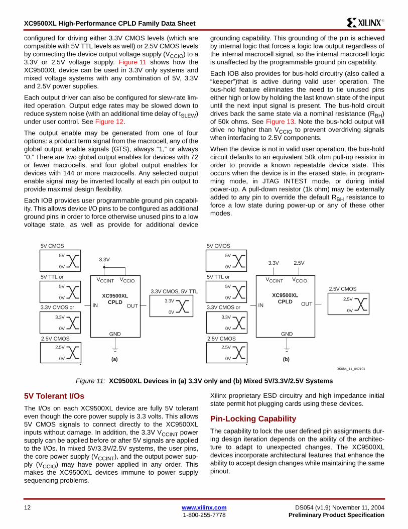
XC9500XL High-Performance CPLD Family Data Sheet R
configured for driving either 33V CMOS levels (which arecompatible with 5V TTL levels as well) or 25V CMOS levelsby connecting the device output voltage supply (VCCIO) to a33V or 25V voltage supply Figure 11 shows how theXC9500XL device can be used in 33V only systems andmixed voltage systems with any combination of 5V 33Vand 25V power supplies
Each output driver can also be configured for slew-rate lim-ited operation Output edge rates may be slowed down toreduce system noise (with an additional time delay of tSLEW)under user control See Figure 12
The output enable may be generated from one of fouroptions a product term signal from the macrocell any of theglobal output enable signals (GTS) always ldquo1rdquo or alwaysldquo0rdquo There are two global output enables for devices with 72or fewer macrocells and four global output enables fordevices with 144 or more macrocells Any selected outputenable signal may be inverted locally at each pin output toprovide maximal design flexibility
Each IOB provides user programmable ground pin capabil-ity This allows device IO pins to be configured as additionalground pins in order to force otherwise unused pins to a lowvoltage state as well as provide for additional device
grounding capability This grounding of the pin is achievedby internal logic that forces a logic low output regardless ofthe internal macrocell signal so the internal macrocell logicis unaffected by the programmable ground pin capability
Each IOB also provides for bus-hold circuitry (also called aldquokeeperrdquo)that is active during valid user operation Thebus-hold feature eliminates the need to tie unused pinseither high or low by holding the last known state of the inputuntil the next input signal is present The bus-hold circuitdrives back the same state via a nominal resistance (RBH)of 50k ohms See Figure 13 Note the bus-hold output willdrive no higher than VCCIO to prevent overdriving signalswhen interfacing to 25V components
When the device is not in valid user operation the bus-holdcircuit defaults to an equivalent 50k ohm pull-up resistor inorder to provide a known repeatable device state Thisoccurs when the device is in the erased state in program-ming mode in JTAG INTEST mode or during initialpower-up A pull-down resistor (1k ohm) may be externallyadded to any pin to override the default RBH resistance toforce a low state during power-up or any of these othermodes
5V Tolerant IOsThe IOs on each XC9500XL device are fully 5V toleranteven though the core power supply is 33 volts This allows5V CMOS signals to connect directly to the XC9500XLinputs without damage In addition the 33V VCCINT powersupply can be applied before or after 5V signals are appliedto the IOs In mixed 5V33V25V systems the user pinsthe core power supply (VCCINT) and the output power sup-ply (VCCIO) may have power applied in any order Thismakes the XC9500XL devices immune to power supplysequencing problems
Xilinx proprietary ESD circuitry and high impedance initialstate permit hot plugging cards using these devices
Pin-Locking CapabilityThe capability to lock the user defined pin assignments dur-ing design iteration depends on the ability of the architec-ture to adapt to unexpected changes The XC9500XLdevices incorporate architectural features that enhance theability to accept design changes while maintaining the samepinout
Figure 11 XC9500XL Devices in (a) 33V only and (b) Mixed 5V33V25V Systems
IN OUT
25V33V
GND
(b)
25V CMOS
IN OUT
XC9500XLCPLD
XC9500XLCPLD
VCCINT VCCIO VCCINT VCCIO
33V
GND
(a)
33V
0V
5V
0V
33V
0V
25V
0V
25V
0V
33V CMOS 5V TTL
DS054_11_042101
25V CMOS
33V CMOS or
5V TTL or
5V
0V
5V CMOS
5V
0V
33V
0V
25V
0V
25V CMOS
33V CMOS or
5V TTL or
5V
0V
5V CMOS
12 wwwxilinxcom DS054 (v19) November 11 20041-800-255-7778 Preliminary Product Specification
XC9500XL High-Performance CPLD Family Data SheetR
The XC9500XL architecture provides for superior pin-lock-ing characteristics with a combination of large number ofrouting switches in the FastCONNECT II switch matrix a54-wide input Function Block and flexible bi-directionalproduct term allocation within each macrocell These fea-tures address design changes that require adding or chang-ing internal routing including additional signals into existingequations or increasing equation complexity respectively
For extensive design changes requiring higher logic capac-ity than is available in the initially chosen device the newdesign may be able to fit into a larger pin-compatible deviceusing the same pin assignments The same board may beused with a higher density device without the expense ofboard rework
In-System ProgrammingOne or more XC9500XL devices can be daisy chainedtogether and programmed in-system via a standard 4-pinJTAG protocol as shown in Figure 14 In-system program-ming offers quick and efficient design iterations and elimi-nates package handling The Xilinx development systemprovides the programming data sequence using a Xilinxdownload cable a third-party JTAG development systemJTAG-compatible board tester or a simple microprocessorinterface that emulates the JTAG instruction sequence
All IOs are 3-stated and pulled high by the bus-hold cir-cuitry during in-system programming If a particular signalmust remain low during this time then a pulldown resistormay be added to the pin
External ProgrammingXC9500XL devices can also be programmed by the XilinxHW-130 device programmer as well as third-party program-mers This provides the added flexibility of using pre-pro-grammed devices during manufacturing with an in-systemprogrammable option for future enhancements and designchanges
Reliability and EnduranceAll XC9500XL CPLDs provide a minimum endurance levelof 10000 in-system programerase cycles and a minimumdata retention of 20 years Each device meets all functionalperformance and data retention specifications within thisendurance limit
IEEE 11491 Boundary-Scan (JTAG)XC9500XL devices fully support IEEE 11491 bound-ary-scan (JTAG) EXTEST SAMPLEPRELOAD BYPASSUSERCODE INTEST IDCODE HIGHZ and CLAMPinstructions are supported in each device Additionalinstructions are included for in-system programming opera-tions
Figure 12 Output Slew-Rate Control For (a) Rising and (b) Falling Outputs
Time0 0
15V
Standard
OutputVoltage
(a)
Slew-Rate Limited
Time
OutputVoltage
(b)
Standard
Slew-Rate Limited
VCCIO
TSLEW TSLEW
15V
DS054_12_042101
Figure 13 Bus-Hold Logic
RBH
IO
Set to PINduring valid useroperation Drive to
VCCIO Level
PIN
0
DS054_13_042101
DS054 (v19) November 11 2004 wwwxilinxcom 13Preliminary Product Specification 1-800-255-7778
XC9500XL High-Performance CPLD Family Data Sheet R
Design SecurityXC9500XL devices incorporate advanced data security fea-tures which fully protect the programming data againstunauthorized reading or inadvertent device erasurerepro-gramming Table 3 shows the four different security settingsavailable
The read security bits can be set by the user to prevent theinternal programming pattern from being read or copiedWhen set they also inhibit further program operations butallow device erase Erasing the entire device is the only wayto reset the read security bit
The write security bits provide added protection againstaccidental device erasure or reprogramming when theJTAG pins are subject to noise such as during systempower-up Once set the write-protection may be deacti-
vated when the device needs to be reprogrammed with avalid pattern with a specific sequence of JTAG instructions
Low Power Mode All XC9500XL devices offer a low-power mode for individualmacrocells or across all macrocells This feature allows thedevice power to be significantly reduced
Each individual macrocell may be programmed inlow-power mode by the user Performance-critical parts ofthe application can remain in standard power mode whileother parts of the application may be programmed forlow-power operation to reduce the overall power dissipa-tion Macrocells programmed for low-power mode incuradditional delay (tLP) in pin-to-pin combinatorial delay aswell as register setup time Product term clock to output andproduct term output enable delays are unaffected by themacrocell power-setting Signals switching at rates lessthan 50 ns risefall time should be assigned to the macro-cells configured in low power mode
Timing ModelThe uniformity of the XC9500XL architecture allows a sim-plified timing model for the entire device The basic timingmodel shown in Figure 15 is valid for macrocell functionsthat use the direct product terms only with standard powersetting and standard slew rate setting Table 4 shows howeach of the key timing parameters is affected by the productterm allocator (if needed) low-power setting and slew-lim-ited setting
The product term allocation time depends on the logic spanof the macrocell function which is defined as one less thanthe maximum number of allocators in the product term pathIf only direct product terms are used then the logic span is0 The example in Figure 6 shows that up to 15 productterms are available with a span of 1 In the case of Figure 7the 18 product term function has a span of 2
Table 3 Data Security Options
Read Security
Default Set
Writ
e Se
curit
y DefaultRead AllowedProgramErase
Allowed
Read InhibitedProgram Inhibited
Erase Allowed
SetRead AllowedProgramErase
Allowed
Read InhibitedProgramErase
Inhibited
Figure 14 System Programming Operation (a) Solder Device to PCB and (b) Program Using Download Cable
X5902
GND
V CC
(a) (b)
14 wwwxilinxcom DS054 (v19) November 11 20041-800-255-7778 Preliminary Product Specification
XC9500XL High-Performance CPLD Family Data SheetR
Detailed timing information may be derived from the full tim-ing model shown in Figure 16 The values and explanations
for each parameter are given in the individual device datasheets
Figure 15 Basic Timing Model
Figure 16 Detailed Timing Model
CombinatorialLogic
Propagation Delay = TPD(a)
CombinatorialLogic
Setup Time = TSU
TCO
TPSU
TPCO
Clock to Out Time = TCO(b)
DT Q
CombinatorialLogic
Internal System Cycle Time = TSYSTEM
DS054_15_042101
(d)
DT Q
CombinatorialLogic
Setup Time = TPSU Clock to Out Time = TPCO(c)
P-Term ClockPath
DT Q
DT Q
SR
TIN
TLOGILP STPTA
TF
TPDI
TSUI TCOITHI
TAOITRAI
TOUT
TSLEW
TEN
DS054_16_042101
TLOGI
TPTCK
TPTSR
TPTTS
TGCK
TGSR
TGTS
Macrocell
CE
DS054 (v19) November 11 2004 wwwxilinxcom 15Preliminary Product Specification 1-800-255-7778
XC9500XL High-Performance CPLD Family Data Sheet R
Power-Up CharacteristicsThe XC9500XL devices are well behaved under all operat-ing conditions During power-up each XC9500XL deviceemploys internal circuitry which keeps the device in the qui-escent state until the VCCINT supply voltage is at a safe level(approximately 25V) During this time all device pins andJTAG pins are disabled and all device outputs are disabledwith the pins weakly pulled high as shown in Table 5 Whenthe supply voltage reaches a safe level all user registersbecome initialized (typically within 200 micros) and the deviceis immediately available for operation as shown inFigure 17
If the device is in the erased state (before any user patternis programmed) the device outputs remain disabled withweak pull-up The JTAG pins are enabled to allow thedevice to be programmed at any time All devices areshipped in the erased state from the factory
If the device is programmed the device inputs and outputstake on their configured states for normal operation TheJTAG pins are enabled to allow device erasure or bound-ary-scan tests at any time
Development System SupportThe XC9500XL family and associated in-system program-ming capabilities are fully supported in either software solu-tions available from Xilinx
The Foundation Series is an all-in-one development systemcontaining schematic entry HDL (VHDL Verilog and
ABEL) and simulation capabilities It supports theXC9500XL family as well as other CPLD and FPGA fami-lies
The Alliance Series includes CPLD and FPGA implementa-tion technology as well as all necessary libraries and inter-faces for Alliance partner EDA solutions
FastFLASH TechnologyAn advanced 035 micron feature size CMOS Flash process isused to fabricate all XC9500XL devices The FastFLASH pro-cess provides high performance logic capability fast pro-gramming times and superior reliability and enduranceratings
Figure 17 Device Behavior During Power-up
VCCINT
NoPower
38 V(Typ)
0VNo
PowerQuiescent
StateQuiescent
StateUser Operation
Initialization of User Registers
DS054_17_042101
25V(Typ)
Table 4 Timing Model Parameters
Parameter DescriptionProduct TermAllocator(1)
MacrocellLow-Power Setting
Output Slew-Limited
SettingTPD Propagation Delay + TPTA S + TLP + TSLEWTSU Global Clock Setup Time + TPTA S + TLP ndashTCO Global Clock-to-output - - + TSLEWTPSU Product Term Clock Setup Time + TPTA S + TLP -TPCO Product Term Clock-to-output - - + TSLEW
TSYSTEM Internal System Cycle Period + TPTA S + TLP -Notes 1 S = the logic span of the function as defined in the text
Table 5 XC9500XL Device CharacteristicsDevice Circuitry Quiescent State Erased Device Operation Valid User Operation
IOB Bus-Hold Pull-up Pull-up Bus-HoldDevice Outputs Disabled Disabled As ConfiguredDevice Inputs and Clocks Disabled Disabled As ConfiguredFunction Block Disabled Disabled As ConfiguredJTAG Controller Disabled Enabled Enabled
16 wwwxilinxcom DS054 (v19) November 11 20041-800-255-7778 Preliminary Product Specification
XC9500XL High-Performance CPLD Family Data SheetR
Further ReadingThe following Xilinx links go to relevant XC9500XL CPLDdocumentation
Data Sheets Application Notes and White PapersPackagingOnline Store
Revision HistoryThe following table shows the revision history for this document
Date Version Revision
092898 10 Initial Xilinx release
100298 11 Figure 1 correction
020399 12 Included hot socket reference revised layout BGA package change for XC95288XL
040299 13 Minor typesetting corrections
060799 14 Minor typesetting corrections
060799 15 Added CS280 package
012502 16 Added DS054 data sheet number Added 44-pin VQFP package Updated Device Family table
020703 17 Added Further Reading section
080204 18 Added Pb-free documentation
111104 19 Changes to package designations in Table 2 on page 2
DS054 (v19) November 11 2004 wwwxilinxcom 17Preliminary Product Specification 1-800-255-7778
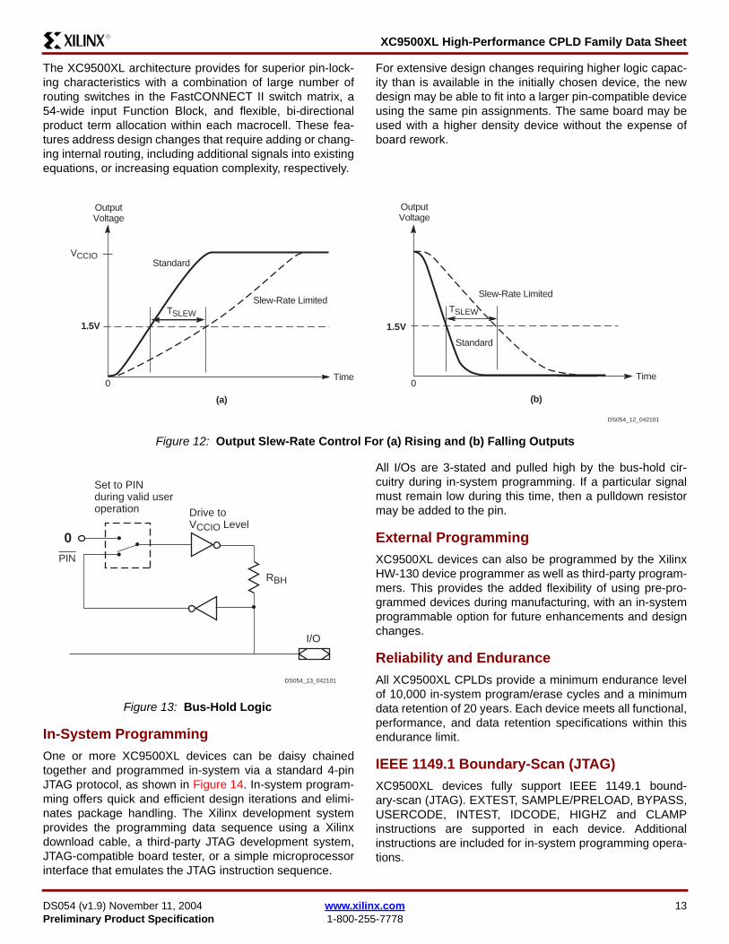
XC9500XL High-Performance CPLD Family Data SheetR
The XC9500XL architecture provides for superior pin-lock-ing characteristics with a combination of large number ofrouting switches in the FastCONNECT II switch matrix a54-wide input Function Block and flexible bi-directionalproduct term allocation within each macrocell These fea-tures address design changes that require adding or chang-ing internal routing including additional signals into existingequations or increasing equation complexity respectively
For extensive design changes requiring higher logic capac-ity than is available in the initially chosen device the newdesign may be able to fit into a larger pin-compatible deviceusing the same pin assignments The same board may beused with a higher density device without the expense ofboard rework
In-System ProgrammingOne or more XC9500XL devices can be daisy chainedtogether and programmed in-system via a standard 4-pinJTAG protocol as shown in Figure 14 In-system program-ming offers quick and efficient design iterations and elimi-nates package handling The Xilinx development systemprovides the programming data sequence using a Xilinxdownload cable a third-party JTAG development systemJTAG-compatible board tester or a simple microprocessorinterface that emulates the JTAG instruction sequence
All IOs are 3-stated and pulled high by the bus-hold cir-cuitry during in-system programming If a particular signalmust remain low during this time then a pulldown resistormay be added to the pin
External ProgrammingXC9500XL devices can also be programmed by the XilinxHW-130 device programmer as well as third-party program-mers This provides the added flexibility of using pre-pro-grammed devices during manufacturing with an in-systemprogrammable option for future enhancements and designchanges
Reliability and EnduranceAll XC9500XL CPLDs provide a minimum endurance levelof 10000 in-system programerase cycles and a minimumdata retention of 20 years Each device meets all functionalperformance and data retention specifications within thisendurance limit
IEEE 11491 Boundary-Scan (JTAG)XC9500XL devices fully support IEEE 11491 bound-ary-scan (JTAG) EXTEST SAMPLEPRELOAD BYPASSUSERCODE INTEST IDCODE HIGHZ and CLAMPinstructions are supported in each device Additionalinstructions are included for in-system programming opera-tions
Figure 12 Output Slew-Rate Control For (a) Rising and (b) Falling Outputs
Time0 0
15V
Standard
OutputVoltage
(a)
Slew-Rate Limited
Time
OutputVoltage
(b)
Standard
Slew-Rate Limited
VCCIO
TSLEW TSLEW
15V
DS054_12_042101
Figure 13 Bus-Hold Logic
RBH
IO
Set to PINduring valid useroperation Drive to
VCCIO Level
PIN
0
DS054_13_042101
DS054 (v19) November 11 2004 wwwxilinxcom 13Preliminary Product Specification 1-800-255-7778
XC9500XL High-Performance CPLD Family Data Sheet R
Design SecurityXC9500XL devices incorporate advanced data security fea-tures which fully protect the programming data againstunauthorized reading or inadvertent device erasurerepro-gramming Table 3 shows the four different security settingsavailable
The read security bits can be set by the user to prevent theinternal programming pattern from being read or copiedWhen set they also inhibit further program operations butallow device erase Erasing the entire device is the only wayto reset the read security bit
The write security bits provide added protection againstaccidental device erasure or reprogramming when theJTAG pins are subject to noise such as during systempower-up Once set the write-protection may be deacti-
vated when the device needs to be reprogrammed with avalid pattern with a specific sequence of JTAG instructions
Low Power Mode All XC9500XL devices offer a low-power mode for individualmacrocells or across all macrocells This feature allows thedevice power to be significantly reduced
Each individual macrocell may be programmed inlow-power mode by the user Performance-critical parts ofthe application can remain in standard power mode whileother parts of the application may be programmed forlow-power operation to reduce the overall power dissipa-tion Macrocells programmed for low-power mode incuradditional delay (tLP) in pin-to-pin combinatorial delay aswell as register setup time Product term clock to output andproduct term output enable delays are unaffected by themacrocell power-setting Signals switching at rates lessthan 50 ns risefall time should be assigned to the macro-cells configured in low power mode
Timing ModelThe uniformity of the XC9500XL architecture allows a sim-plified timing model for the entire device The basic timingmodel shown in Figure 15 is valid for macrocell functionsthat use the direct product terms only with standard powersetting and standard slew rate setting Table 4 shows howeach of the key timing parameters is affected by the productterm allocator (if needed) low-power setting and slew-lim-ited setting
The product term allocation time depends on the logic spanof the macrocell function which is defined as one less thanthe maximum number of allocators in the product term pathIf only direct product terms are used then the logic span is0 The example in Figure 6 shows that up to 15 productterms are available with a span of 1 In the case of Figure 7the 18 product term function has a span of 2
Table 3 Data Security Options
Read Security
Default Set
Writ
e Se
curit
y DefaultRead AllowedProgramErase
Allowed
Read InhibitedProgram Inhibited
Erase Allowed
SetRead AllowedProgramErase
Allowed
Read InhibitedProgramErase
Inhibited
Figure 14 System Programming Operation (a) Solder Device to PCB and (b) Program Using Download Cable
X5902
GND
V CC
(a) (b)
14 wwwxilinxcom DS054 (v19) November 11 20041-800-255-7778 Preliminary Product Specification
XC9500XL High-Performance CPLD Family Data SheetR
Detailed timing information may be derived from the full tim-ing model shown in Figure 16 The values and explanations
for each parameter are given in the individual device datasheets
Figure 15 Basic Timing Model
Figure 16 Detailed Timing Model
CombinatorialLogic
Propagation Delay = TPD(a)
CombinatorialLogic
Setup Time = TSU
TCO
TPSU
TPCO
Clock to Out Time = TCO(b)
DT Q
CombinatorialLogic
Internal System Cycle Time = TSYSTEM
DS054_15_042101
(d)
DT Q
CombinatorialLogic
Setup Time = TPSU Clock to Out Time = TPCO(c)
P-Term ClockPath
DT Q
DT Q
SR
TIN
TLOGILP STPTA
TF
TPDI
TSUI TCOITHI
TAOITRAI
TOUT
TSLEW
TEN
DS054_16_042101
TLOGI
TPTCK
TPTSR
TPTTS
TGCK
TGSR
TGTS
Macrocell
CE
DS054 (v19) November 11 2004 wwwxilinxcom 15Preliminary Product Specification 1-800-255-7778
XC9500XL High-Performance CPLD Family Data Sheet R
Power-Up CharacteristicsThe XC9500XL devices are well behaved under all operat-ing conditions During power-up each XC9500XL deviceemploys internal circuitry which keeps the device in the qui-escent state until the VCCINT supply voltage is at a safe level(approximately 25V) During this time all device pins andJTAG pins are disabled and all device outputs are disabledwith the pins weakly pulled high as shown in Table 5 Whenthe supply voltage reaches a safe level all user registersbecome initialized (typically within 200 micros) and the deviceis immediately available for operation as shown inFigure 17
If the device is in the erased state (before any user patternis programmed) the device outputs remain disabled withweak pull-up The JTAG pins are enabled to allow thedevice to be programmed at any time All devices areshipped in the erased state from the factory
If the device is programmed the device inputs and outputstake on their configured states for normal operation TheJTAG pins are enabled to allow device erasure or bound-ary-scan tests at any time
Development System SupportThe XC9500XL family and associated in-system program-ming capabilities are fully supported in either software solu-tions available from Xilinx
The Foundation Series is an all-in-one development systemcontaining schematic entry HDL (VHDL Verilog and
ABEL) and simulation capabilities It supports theXC9500XL family as well as other CPLD and FPGA fami-lies
The Alliance Series includes CPLD and FPGA implementa-tion technology as well as all necessary libraries and inter-faces for Alliance partner EDA solutions
FastFLASH TechnologyAn advanced 035 micron feature size CMOS Flash process isused to fabricate all XC9500XL devices The FastFLASH pro-cess provides high performance logic capability fast pro-gramming times and superior reliability and enduranceratings
Figure 17 Device Behavior During Power-up
VCCINT
NoPower
38 V(Typ)
0VNo
PowerQuiescent
StateQuiescent
StateUser Operation
Initialization of User Registers
DS054_17_042101
25V(Typ)
Table 4 Timing Model Parameters
Parameter DescriptionProduct TermAllocator(1)
MacrocellLow-Power Setting
Output Slew-Limited
SettingTPD Propagation Delay + TPTA S + TLP + TSLEWTSU Global Clock Setup Time + TPTA S + TLP ndashTCO Global Clock-to-output - - + TSLEWTPSU Product Term Clock Setup Time + TPTA S + TLP -TPCO Product Term Clock-to-output - - + TSLEW
TSYSTEM Internal System Cycle Period + TPTA S + TLP -Notes 1 S = the logic span of the function as defined in the text
Table 5 XC9500XL Device CharacteristicsDevice Circuitry Quiescent State Erased Device Operation Valid User Operation
IOB Bus-Hold Pull-up Pull-up Bus-HoldDevice Outputs Disabled Disabled As ConfiguredDevice Inputs and Clocks Disabled Disabled As ConfiguredFunction Block Disabled Disabled As ConfiguredJTAG Controller Disabled Enabled Enabled
16 wwwxilinxcom DS054 (v19) November 11 20041-800-255-7778 Preliminary Product Specification
XC9500XL High-Performance CPLD Family Data SheetR
Further ReadingThe following Xilinx links go to relevant XC9500XL CPLDdocumentation
Data Sheets Application Notes and White PapersPackagingOnline Store
Revision HistoryThe following table shows the revision history for this document
Date Version Revision
092898 10 Initial Xilinx release
100298 11 Figure 1 correction
020399 12 Included hot socket reference revised layout BGA package change for XC95288XL
040299 13 Minor typesetting corrections
060799 14 Minor typesetting corrections
060799 15 Added CS280 package
012502 16 Added DS054 data sheet number Added 44-pin VQFP package Updated Device Family table
020703 17 Added Further Reading section
080204 18 Added Pb-free documentation
111104 19 Changes to package designations in Table 2 on page 2
DS054 (v19) November 11 2004 wwwxilinxcom 17Preliminary Product Specification 1-800-255-7778
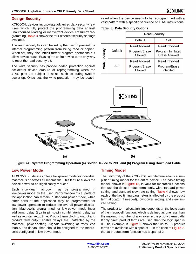
XC9500XL High-Performance CPLD Family Data Sheet R
Design SecurityXC9500XL devices incorporate advanced data security fea-tures which fully protect the programming data againstunauthorized reading or inadvertent device erasurerepro-gramming Table 3 shows the four different security settingsavailable
The read security bits can be set by the user to prevent theinternal programming pattern from being read or copiedWhen set they also inhibit further program operations butallow device erase Erasing the entire device is the only wayto reset the read security bit
The write security bits provide added protection againstaccidental device erasure or reprogramming when theJTAG pins are subject to noise such as during systempower-up Once set the write-protection may be deacti-
vated when the device needs to be reprogrammed with avalid pattern with a specific sequence of JTAG instructions
Low Power Mode All XC9500XL devices offer a low-power mode for individualmacrocells or across all macrocells This feature allows thedevice power to be significantly reduced
Each individual macrocell may be programmed inlow-power mode by the user Performance-critical parts ofthe application can remain in standard power mode whileother parts of the application may be programmed forlow-power operation to reduce the overall power dissipa-tion Macrocells programmed for low-power mode incuradditional delay (tLP) in pin-to-pin combinatorial delay aswell as register setup time Product term clock to output andproduct term output enable delays are unaffected by themacrocell power-setting Signals switching at rates lessthan 50 ns risefall time should be assigned to the macro-cells configured in low power mode
Timing ModelThe uniformity of the XC9500XL architecture allows a sim-plified timing model for the entire device The basic timingmodel shown in Figure 15 is valid for macrocell functionsthat use the direct product terms only with standard powersetting and standard slew rate setting Table 4 shows howeach of the key timing parameters is affected by the productterm allocator (if needed) low-power setting and slew-lim-ited setting
The product term allocation time depends on the logic spanof the macrocell function which is defined as one less thanthe maximum number of allocators in the product term pathIf only direct product terms are used then the logic span is0 The example in Figure 6 shows that up to 15 productterms are available with a span of 1 In the case of Figure 7the 18 product term function has a span of 2
Table 3 Data Security Options
Read Security
Default Set
Writ
e Se
curit
y DefaultRead AllowedProgramErase
Allowed
Read InhibitedProgram Inhibited
Erase Allowed
SetRead AllowedProgramErase
Allowed
Read InhibitedProgramErase
Inhibited
Figure 14 System Programming Operation (a) Solder Device to PCB and (b) Program Using Download Cable
X5902
GND
V CC
(a) (b)
14 wwwxilinxcom DS054 (v19) November 11 20041-800-255-7778 Preliminary Product Specification
XC9500XL High-Performance CPLD Family Data SheetR
Detailed timing information may be derived from the full tim-ing model shown in Figure 16 The values and explanations
for each parameter are given in the individual device datasheets
Figure 15 Basic Timing Model
Figure 16 Detailed Timing Model
CombinatorialLogic
Propagation Delay = TPD(a)
CombinatorialLogic
Setup Time = TSU
TCO
TPSU
TPCO
Clock to Out Time = TCO(b)
DT Q
CombinatorialLogic
Internal System Cycle Time = TSYSTEM
DS054_15_042101
(d)
DT Q
CombinatorialLogic
Setup Time = TPSU Clock to Out Time = TPCO(c)
P-Term ClockPath
DT Q
DT Q
SR
TIN
TLOGILP STPTA
TF
TPDI
TSUI TCOITHI
TAOITRAI
TOUT
TSLEW
TEN
DS054_16_042101
TLOGI
TPTCK
TPTSR
TPTTS
TGCK
TGSR
TGTS
Macrocell
CE
DS054 (v19) November 11 2004 wwwxilinxcom 15Preliminary Product Specification 1-800-255-7778
XC9500XL High-Performance CPLD Family Data Sheet R
Power-Up CharacteristicsThe XC9500XL devices are well behaved under all operat-ing conditions During power-up each XC9500XL deviceemploys internal circuitry which keeps the device in the qui-escent state until the VCCINT supply voltage is at a safe level(approximately 25V) During this time all device pins andJTAG pins are disabled and all device outputs are disabledwith the pins weakly pulled high as shown in Table 5 Whenthe supply voltage reaches a safe level all user registersbecome initialized (typically within 200 micros) and the deviceis immediately available for operation as shown inFigure 17
If the device is in the erased state (before any user patternis programmed) the device outputs remain disabled withweak pull-up The JTAG pins are enabled to allow thedevice to be programmed at any time All devices areshipped in the erased state from the factory
If the device is programmed the device inputs and outputstake on their configured states for normal operation TheJTAG pins are enabled to allow device erasure or bound-ary-scan tests at any time
Development System SupportThe XC9500XL family and associated in-system program-ming capabilities are fully supported in either software solu-tions available from Xilinx
The Foundation Series is an all-in-one development systemcontaining schematic entry HDL (VHDL Verilog and
ABEL) and simulation capabilities It supports theXC9500XL family as well as other CPLD and FPGA fami-lies
The Alliance Series includes CPLD and FPGA implementa-tion technology as well as all necessary libraries and inter-faces for Alliance partner EDA solutions
FastFLASH TechnologyAn advanced 035 micron feature size CMOS Flash process isused to fabricate all XC9500XL devices The FastFLASH pro-cess provides high performance logic capability fast pro-gramming times and superior reliability and enduranceratings
Figure 17 Device Behavior During Power-up
VCCINT
NoPower
38 V(Typ)
0VNo
PowerQuiescent
StateQuiescent
StateUser Operation
Initialization of User Registers
DS054_17_042101
25V(Typ)
Table 4 Timing Model Parameters
Parameter DescriptionProduct TermAllocator(1)
MacrocellLow-Power Setting
Output Slew-Limited
SettingTPD Propagation Delay + TPTA S + TLP + TSLEWTSU Global Clock Setup Time + TPTA S + TLP ndashTCO Global Clock-to-output - - + TSLEWTPSU Product Term Clock Setup Time + TPTA S + TLP -TPCO Product Term Clock-to-output - - + TSLEW
TSYSTEM Internal System Cycle Period + TPTA S + TLP -Notes 1 S = the logic span of the function as defined in the text
Table 5 XC9500XL Device CharacteristicsDevice Circuitry Quiescent State Erased Device Operation Valid User Operation
IOB Bus-Hold Pull-up Pull-up Bus-HoldDevice Outputs Disabled Disabled As ConfiguredDevice Inputs and Clocks Disabled Disabled As ConfiguredFunction Block Disabled Disabled As ConfiguredJTAG Controller Disabled Enabled Enabled
16 wwwxilinxcom DS054 (v19) November 11 20041-800-255-7778 Preliminary Product Specification
XC9500XL High-Performance CPLD Family Data SheetR
Further ReadingThe following Xilinx links go to relevant XC9500XL CPLDdocumentation
Data Sheets Application Notes and White PapersPackagingOnline Store
Revision HistoryThe following table shows the revision history for this document
Date Version Revision
092898 10 Initial Xilinx release
100298 11 Figure 1 correction
020399 12 Included hot socket reference revised layout BGA package change for XC95288XL
040299 13 Minor typesetting corrections
060799 14 Minor typesetting corrections
060799 15 Added CS280 package
012502 16 Added DS054 data sheet number Added 44-pin VQFP package Updated Device Family table
020703 17 Added Further Reading section
080204 18 Added Pb-free documentation
111104 19 Changes to package designations in Table 2 on page 2
DS054 (v19) November 11 2004 wwwxilinxcom 17Preliminary Product Specification 1-800-255-7778
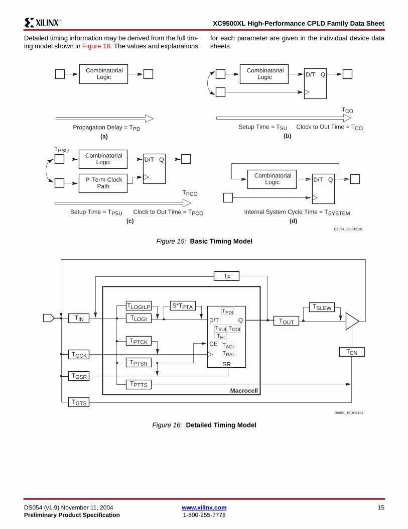
XC9500XL High-Performance CPLD Family Data SheetR
Detailed timing information may be derived from the full tim-ing model shown in Figure 16 The values and explanations
for each parameter are given in the individual device datasheets
Figure 15 Basic Timing Model
Figure 16 Detailed Timing Model
CombinatorialLogic
Propagation Delay = TPD(a)
CombinatorialLogic
Setup Time = TSU
TCO
TPSU
TPCO
Clock to Out Time = TCO(b)
DT Q
CombinatorialLogic
Internal System Cycle Time = TSYSTEM
DS054_15_042101
(d)
DT Q
CombinatorialLogic
Setup Time = TPSU Clock to Out Time = TPCO(c)
P-Term ClockPath
DT Q
DT Q
SR
TIN
TLOGILP STPTA
TF
TPDI
TSUI TCOITHI
TAOITRAI
TOUT
TSLEW
TEN
DS054_16_042101
TLOGI
TPTCK
TPTSR
TPTTS
TGCK
TGSR
TGTS
Macrocell
CE
DS054 (v19) November 11 2004 wwwxilinxcom 15Preliminary Product Specification 1-800-255-7778
XC9500XL High-Performance CPLD Family Data Sheet R
Power-Up CharacteristicsThe XC9500XL devices are well behaved under all operat-ing conditions During power-up each XC9500XL deviceemploys internal circuitry which keeps the device in the qui-escent state until the VCCINT supply voltage is at a safe level(approximately 25V) During this time all device pins andJTAG pins are disabled and all device outputs are disabledwith the pins weakly pulled high as shown in Table 5 Whenthe supply voltage reaches a safe level all user registersbecome initialized (typically within 200 micros) and the deviceis immediately available for operation as shown inFigure 17
If the device is in the erased state (before any user patternis programmed) the device outputs remain disabled withweak pull-up The JTAG pins are enabled to allow thedevice to be programmed at any time All devices areshipped in the erased state from the factory
If the device is programmed the device inputs and outputstake on their configured states for normal operation TheJTAG pins are enabled to allow device erasure or bound-ary-scan tests at any time
Development System SupportThe XC9500XL family and associated in-system program-ming capabilities are fully supported in either software solu-tions available from Xilinx
The Foundation Series is an all-in-one development systemcontaining schematic entry HDL (VHDL Verilog and
ABEL) and simulation capabilities It supports theXC9500XL family as well as other CPLD and FPGA fami-lies
The Alliance Series includes CPLD and FPGA implementa-tion technology as well as all necessary libraries and inter-faces for Alliance partner EDA solutions
FastFLASH TechnologyAn advanced 035 micron feature size CMOS Flash process isused to fabricate all XC9500XL devices The FastFLASH pro-cess provides high performance logic capability fast pro-gramming times and superior reliability and enduranceratings
Figure 17 Device Behavior During Power-up
VCCINT
NoPower
38 V(Typ)
0VNo
PowerQuiescent
StateQuiescent
StateUser Operation
Initialization of User Registers
DS054_17_042101
25V(Typ)
Table 4 Timing Model Parameters
Parameter DescriptionProduct TermAllocator(1)
MacrocellLow-Power Setting
Output Slew-Limited
SettingTPD Propagation Delay + TPTA S + TLP + TSLEWTSU Global Clock Setup Time + TPTA S + TLP ndashTCO Global Clock-to-output - - + TSLEWTPSU Product Term Clock Setup Time + TPTA S + TLP -TPCO Product Term Clock-to-output - - + TSLEW
TSYSTEM Internal System Cycle Period + TPTA S + TLP -Notes 1 S = the logic span of the function as defined in the text
Table 5 XC9500XL Device CharacteristicsDevice Circuitry Quiescent State Erased Device Operation Valid User Operation
IOB Bus-Hold Pull-up Pull-up Bus-HoldDevice Outputs Disabled Disabled As ConfiguredDevice Inputs and Clocks Disabled Disabled As ConfiguredFunction Block Disabled Disabled As ConfiguredJTAG Controller Disabled Enabled Enabled
16 wwwxilinxcom DS054 (v19) November 11 20041-800-255-7778 Preliminary Product Specification
XC9500XL High-Performance CPLD Family Data SheetR
Further ReadingThe following Xilinx links go to relevant XC9500XL CPLDdocumentation
Data Sheets Application Notes and White PapersPackagingOnline Store
Revision HistoryThe following table shows the revision history for this document
Date Version Revision
092898 10 Initial Xilinx release
100298 11 Figure 1 correction
020399 12 Included hot socket reference revised layout BGA package change for XC95288XL
040299 13 Minor typesetting corrections
060799 14 Minor typesetting corrections
060799 15 Added CS280 package
012502 16 Added DS054 data sheet number Added 44-pin VQFP package Updated Device Family table
020703 17 Added Further Reading section
080204 18 Added Pb-free documentation
111104 19 Changes to package designations in Table 2 on page 2
DS054 (v19) November 11 2004 wwwxilinxcom 17Preliminary Product Specification 1-800-255-7778
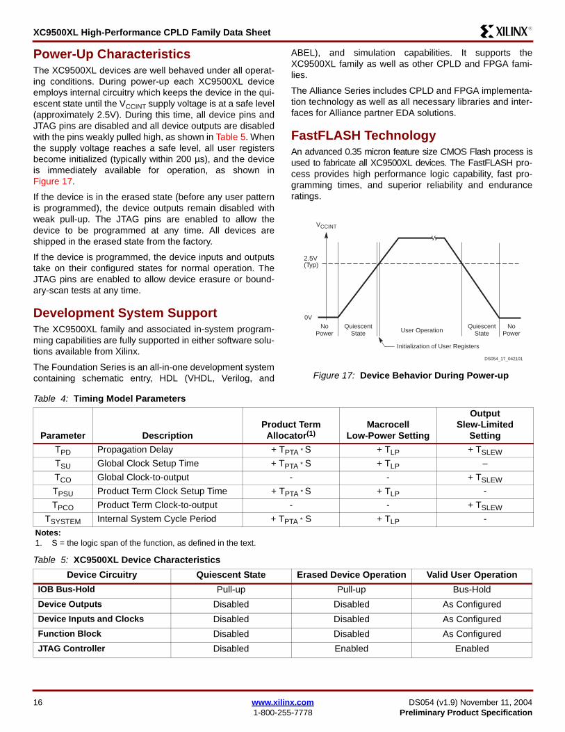