Embed Size (px)
Citation preview

www.fei.edu.brMOS-AK Workshop, ESSDERC, Leuven, 2017
Junctionless Nanowire Transistors
Performance: Static and Dynamic
Modeling
Marcelo Antonio [email protected]
1
Department of Electrical Engineering
Centro Universitario FEI
Av. Humberto de Alencar Castelo Branco, 3972
09850-901 – São Bernardo do Campo, Brazil

www.fei.edu.br | MOS-AK Workshop, ESSDERC, Leuven, 2017
Introduction & Motivation
Compact Modeling
Conclusion
The Junctionless Nanowire Transistor
Outline
Static Drain Current Model
Dynamic Model

www.fei.edu.br | MOS-AK Workshop, ESSDERC, Leuven, 2017
Introduction & Motivation
Compact Modeling
Conclusion
The Junctionless Nanowire Transistor
Outline
Static Drain Current Model
Dynamic Model

www.fei.edu.br | MOS-AK Workshop, ESSDERC, Leuven, 2017
Moore’s Law: The number of devices per chip double each
two years

www.fei.edu.br | MOS-AK Workshop, ESSDERC, Leuven, 2017
Reduction on cost/function
Performance improvement
time
Scaling
L=35nm
SiGe
L=35nmL=35nm
SiGe
NiSi
25 nm
NiSi
25 nm
FUSI
strain
HfO2
high -k
metal gate
FinFET
USJ
Active Area
Gate FieldSpacers
Active Area
Gate FieldSpacers
Active Area
Gate FieldSpacers
Ge/IIIV
silicide
ArF immersion
hyper NAimmersion
ArF + RET
EUVL
Courtesy of Prof. Cor Claeys

www.fei.edu.br | MOS-AK Workshop, ESSDERC, Leuven, 2017
Gate
Source Drain
Buried oxide
Back gate (substrate)
Source
Drain
Gate
ID
Buried oxide
Tri-Gate with 800C 600Torr 5min H2Anneal
Fins are 45x78nm, Nice corner rounding by H2 anneal
20 nm
Polysilicon Gate
Silicon
Fin
Buried Oxide
Gate
Source Drain
BOX
Gat
e
Gat
e
“1 Gate”
“2 Gates”
“3 Gates”
Evolution of Transistors
“Gate-all-Around”
Courtesy Dr. Jean-Pierre Colinge

www.fei.edu.br | MOS-AK Workshop, ESSDERC, Leuven, 2017

www.fei.edu.br | MOS-AK Workshop, ESSDERC, Leuven, 2017
Introduction & Motivation
Compact Modeling
Conclusion
The Junctionless Nanowire Transistor
Outline
Static Drain Current Model
Dynamic Model

www.fei.edu.br | MOS-AK Workshop, ESSDERC, Leuven, 2017
• The Junctionless Nanowire Transistor (JNT) Developed in 2009 by J.P. Colinge et al.[1].
➢ Absence of doping gradients;
➢ Avoids impurity diffusion into
the channel region;
➢ Presents doping concentration in
the order of 1019 cm-3;
Junctionless IM Trigate
9
Introduction & Motivation
SBMicro 2014 - 29th Symposium on Microelectronics Technology and Devices
[1] J. P Colinge et al., in: SOI Conference (2009).

www.fei.edu.br | MOS-AK Workshop, ESSDERC, Leuven, 2017 10
Introduction
SBMicro 2014 - 29th Symposium on Microelectronics Technology and Devices
• The Junctionless Nanowire Transistor
With respect to inversion mode devices:
Advantages Drawbacks➢ Reduced electric field;
➢ Smaller mobility degradation;
➢ Better analog properties;
➢ Better DIBL;
➢ Reduced low frequency noise.
➢Strong dependence of VTH on the
fin dimensions;
➢ Higher Series Resistance;
➢ Smaller low field mobility.

www.fei.edu.br | MOS-AK Workshop, ESSDERC, Leuven, 2017
A
B
C
5 nm
11
Junctionless nanowire transistor - (3 parallel nanowires)
Courtesy Dr. Jean-Pierre Colinge

www.fei.edu.br | MOS-AK Workshop, ESSDERC, Leuven, 2017
Performance Comparison: Inversion-Mode and Junctionless nanowire transistors
- Common parameters in JNT and IM:
✓EOT=1.3 nm
✓tSi = 10 nm
✓ Wfin > 10 nm
✓ L = down to 10 nm
- JNT Characteristics:
✓ND = 1.1019 cm-3
- IM Characteristics:
✓ NA = 1.1015 cm-3

www.fei.edu.br | MOS-AK Workshop, ESSDERC, Leuven, 2017
Comparison between IM and Junctionless nanowire transistors of similar dimensions
10-13
10-10
10-7
10-4
-0.50 -0.25 0.00 0.25 0.5010
-13
10-10
10-7
10-4
I DS/(
W/L
) [A
]
L = 100 nm
L = 30 nm
L = 10 nm
Junctionless TransistorsExperimental Data
0
1
2
3
ID
S/(
W/L
) [
A]
Nanowire Transistors L = 100 nm
L = 30 nm
L = 10 nmH
fin = 10 nm
Wfin
= 10 nm
VDS
= 50 mVI DS [A
]/(W
/L)
VGS
-VTH
[V]
0
3
6
9
ID
S/(
W/L
) [
A]
Higher IDS
BetterSubthreshold
Swing
Drain current vs. VGT - L down to 10 nm
R. T. Doria et at., IEEE S3S Conference, 2017

www.fei.edu.br | MOS-AK Workshop, ESSDERC, Leuven, 2017
Comparison between IM and Junctionless nanowire transistors of similar dimensions
Smallerthreshold
voltage roll-off
Nearly ideal Subthreshold
Swing
0.38
0.40
0.42
0.44
10 100-2.00
-1.50
-1.00
-0.50
0.00
0.50
VTH
VT
H [V
]
Junctionless Transistors
60
62
64
SS
SS
[m
V/d
ec]
Wfin
= 10 nm
VDS
= 50 mV
VT
H [V
]
L [nm]
Nanowire Transistors
60
120
180
240
SS
[m
V/d
ec]
VTH and Subthrehsold Swing (SS) vs. L
R. T. Doria et at., IEEE S3S Conference, 2017

www.fei.edu.br | MOS-AK Workshop, ESSDERC, Leuven, 2017
10 1000.01
0.1
1
Junctionless
Nanowires
Wfin
= 10 nm
DIB
L [m
V/V
]
L [m]
Comparison between IM and Junctionless nanowire transistors of similar dimensions
VDS1 = 50 mV
VDS2 = 1.0 V
Drain Induced Barrier Lowering (DIBL) vs. L
R. T. Doria et at., IEEE S3S Conference, 2017

www.fei.edu.br | MOS-AK Workshop, ESSDERC, Leuven, 2017
Comparison between IM and Junctionless nanowire transistors of similar dimensions
ION and IOFF vs. L
10-6
10-5
10-4
10 10010-13
10-11
10-9
10-7
ION
@ VGS
- VTH
= 0.5 V
Closed Symbols - JNTs
Open Symbols - NWs
I ON [A
]
I OF
F [A
]
L [nm]
IOFF
@ VGS
- VTH
= -0.3 VVDS
= 1 V
Wfin
= 10 nm
Hfin
= 10 nm
Smaller ION
Smaller IOFF
Lower carrier mobility
Better electrostatic control
Longer L in subthreshold
R. T. Doria et at., IEEE S3S Conference, 2017

www.fei.edu.br | MOS-AK Workshop, ESSDERC, Leuven, 2017
Comparison between IM and Junctionless nanowire transistors of similar dimensions
ION/IOFF vs. L
Larger ION/IOFF at all L
Smaller IOFF
10 100101
103
105
107
I ON/I
OF
F
L [nm]
, VDS
= 50 mV
, VDS
= 1 V
Open Symbols - NWs
Closed Symbols - JNTs
Wfin
= 10 nm
Hfin
= 10 nm
R. T. Doria et at., IEEE S3S Conference, 2017

www.fei.edu.br | MOS-AK Workshop, ESSDERC, Leuven, 2017
Comparison between IM and Junctionless nanowire transistors of similar dimensions
gmmax and RS vs. L
Smaller gmmax at all L
Larger RS
0 50 100 150 20010
-6
10-5
gm
ma
x [
]
L [nm]
gmmax
,
,
,
0
5
10
15
RS
Nanowires
Junctionless
RS [k
]
Wfin
= 10 nm
VDS
= 50 mV
Lower carrier mobility
Not optimized S/D extensions
R. T. Doria et at., IEEE S3S Conference, 2017

www.fei.edu.br | MOS-AK Workshop, ESSDERC, Leuven, 2017
Comparison between IM and Junctionless nanowire transistors of similar dimensions
ION,IOFF and ION/IOFF vs. WFinSmaller ION
Smaller IOFF
Lower carrier mobility
Better electrostatic control
Longer L in subthreshold
0 20 40 60 80 100 120
10-10
10-8
10-6
10-4
VDS
= 1 V
L = 100 nm
Hfin
= 10 nm
ION
@ VGS
- VTH
= 0.5 V
IOFF
@ VGS
- VTH
= -0.3 V
I ON, I O
FF [A
]
Wfin
[nm]
Open Symbols - NWs
Closed Symbols - JNTs
104
105
106
107
108
IO
N/I
OF
F
Larger ION/IOFF at all WFin
R. T. Doria et at., IEEE S3S Conference, 2017

www.fei.edu.br | MOS-AK Workshop, ESSDERC, Leuven, 2017
Comparison between IM and Junctionless nanowire transistors of similar dimensions
SS and DIBL vs. WFin
Better DIBL for Wfin<60 nm
0 20 40 60 80 100 120
60
62
64
66
68
L = 100 nm
Hfin
= 10 nm
Open Symbols - NWs
Closed Symbols - JNTs
SS
[m
V/d
ec]
Wfin
[nm]
10
20
30
40
50
60
DIB
L [m
V/V
]
Better SubthresholdSwing at all WFin
R. T. Doria et at., IEEE S3S Conference, 2017

www.fei.edu.br | MOS-AK Workshop, ESSDERC, Leuven, 2017
Introduction & Motivation
Compact Modeling
Conclusion
The Junctionless Nanowire Transistor
Outline
Static Drain Current Model
Dynamic Model

www.fei.edu.br | MOS-AK Workshop, ESSDERC, Leuven, 2017 22
Long Channel Drain Current Model
▪ 2D Poisson equation (considering only the depletion charge):
▪ Using the approximation:
Bulk conduction
Poisson equation can be integrated, leading to:
dz
d
dx
d ΦΦ
and considering the center potential as zero at the source side
dΦNq
dx
dΦd
Si
D
22
2
Si
D
ε
Nq
dz
Φd
dx
Φd
2
2
2
2
SideplSDdeplS εNqE /Φ ,,
TREVISOLI, R.. D ; DORIA, R. T. ; DE SOUZA, M. ; DAS, S. ; FERAIN, I. ; PAVANELLO, M. A. . Surface
Potential-Based Drain Current Analytical Model for Triple-Gate Junctionless Nanowire Transistors. IEEE
Transactions on Electron Devices, v. 59, p. 3510-3518, 2012.

www.fei.edu.br | MOS-AK Workshop, ESSDERC, Leuven, 2017 23
Long Channel Drain Current Model
▪ Approximation:dz
d
dx
d ΦΦ
-6 -4 -2 0 2 4 6
-0.12
-0.08
-0.04
0.00
Left surface
=-0.11 V
Right surface
=-0.11 V
Top surface
=-0.12 V
xz
Pote
ntial [V
]
x,z [nm]
zx
-6 -4 -2 0 2 4 6
0
1
2
3
4
Exz
Ezx
Ele
ctr
ic fie
ld [x10
5 V
/cm
]x,z [nm]
ERight surface
=4.16 x10⁵ V/cm
ETop surface
=4.04 x10⁵ V/cm
ELeft surface
=4.16 x10⁵ V/cm

www.fei.edu.br | MOS-AK Workshop, ESSDERC, Leuven, 2017 24
Long Channel Drain Current Model
▪ Relation between depletion charge and electric field:
Bulk conduction
MOS capacitor:
SideplSDS εNqE /Φ ,
)2(ε FinFinSSiDepl WHEQ
DeploxFBGdeplS Q)CVV( ,Φ a = Si q ND (2HFin + WFin)2
)(22
2
2
22, FBG
oxoxox
FBGdeplS VVCCC
VV
aaa

www.fei.edu.br | MOS-AK Workshop, ESSDERC, Leuven, 2017 25
Long Channel Drain Current Model
▪ 2D Poisson equation:
Accumulation conduction
Poisson equation can be integrated, leading to:
t
Si
D eε
Nq
dz
Φd
dx
Φd
/
2
2
2
2
SitaccStDaccS εNqE /)1)/Φ(exp( ,,
t
oxaccSFBG
taccS
CVV
a
22
,
,
)Φ(1lnΦ
An exact solution for ΦS,acc can be obtained by the use of the Lambert function.
However, in order to obtain a simplified solution, as ΦS,acc values a few ϕt in strong
accumulation, ΦS,acc can be neglected for VG >> VFB inside the logarithm term.

www.fei.edu.br | MOS-AK Workshop, ESSDERC, Leuven, 2017 26
Long Channel Drain Current Model
▪ Transition between bulk and accumulation conductionto have a continuous transition between both conduction regimes (bulk conduction and both
accumulation layer and bulk conductions), a smooth function has been used to VG [24]:
))exp(1ln(
]))/)(1(exp(1ln[1
1
1
2A
VVyVAVV FBG
FBG
where A1 controls the smoothness and has been set to 12 and Vy is the voltage at the point y of the channel, i.e.
Vy = 0 at source and Vy = VD at drain for the calculation of the source and drain surface potentials, respectively.
This equation is used to limit the maximum gate voltage in VFB. This
function is used inside the square root term of Φs,depl instead of VG, so that
the depletion charge smoothly tends to zero at the flatband condition.

www.fei.edu.br | MOS-AK Workshop, ESSDERC, Leuven, 2017 27
Long Channel Drain Current Model
▪ Transition between subthreshold and above threshold regimes
This equation limits the minimum gate voltage in the threshold voltage,
such that the conduction charge reduces exponentially.
))exp(1ln(
]))/1(exp(1ln[1
2
22
3A
VVAVV TG
TG
where A2 is related to the subthreshold slope, calculated as A2 = VT/(2.n.ϕt),
where n is the body factor which is close to the unity for these devices.

www.fei.edu.br | MOS-AK Workshop, ESSDERC, Leuven, 2017 28
Long Channel Drain Current Model
▪ General solution
accSdeplSS ,,
)(22
32
2
222, FBG
oxoxox
FBGdeplS VVCCC
VyVV
aaa
t
oxGG
taccS
CVV
a
22
2
,
)(1lnΦ

www.fei.edu.br | MOS-AK Workshop, ESSDERC, Leuven, 2017 29
Long Channel Drain Current Model
▪ The drain current can be obtained by:
dy
dVyQI nD nμ
oxSGFBDfn )CV(VHWNqQQQ Φ
ox
DnSn
DC
LI
2
)(μ2
,
2
,n

www.fei.edu.br | MOS-AK Workshop, ESSDERC, Leuven, 2017 30
Long Channel Drain Current Model
Saturation voltage satsatDsat vQI
The drain current IDsat is obtained by considering Qn,D = Qsat. Therefore, Qsat can be
isolated, reaching:
2
,
2
nn μμSn
oxsat
oxsatsat Q
CLv
CLvQ
GFB
oxox
fsat
Dsat VVCC
QQV
22
11
22 aaa
))exp(1ln(
]))/1(exp(1ln[1
3
3
A
VVAVV DsatD
DsatD

www.fei.edu.br | MOS-AK Workshop, ESSDERC, Leuven, 2017 31
Long Channel Drain Current Model
• Three-dimensional simulations were performed in Sentaurus
• Device characteristics
▪ channel length = 1 m
▪ N+ polysilicon gate
▪ tSi = 10 nm
▪ ND = 1 x 1019 cm-3
▪ tox = 2 nm
▪ W = 10 nm
• Low Field Mobility was considered as 100 cm2/V.s

www.fei.edu.br | MOS-AK Workshop, ESSDERC, Leuven, 2017
0.0 0.4 0.8 1.2 1.6
-0.8
-0.4
0.0
0.4
0.8
Surface potential at source
lines - model
symbols - simulation
ND = 1 x 10
19 cm
-3
H = 10 nm
W = 10 nm
tox
= 2 nm
L = 1 m
Effective
Surf
ace P
ote
ntia
l [V
]
Gate voltage [V]
Surface potential at drain
for VD = 0.1, 0.2 and 0.5V > V
D
Good Agreementbetween simulatedand modeled data
for various VDS
Long Channel Drain Current Model

www.fei.edu.br | MOS-AK Workshop, ESSDERC, Leuven, 2017
Good Agreementbetween simulatedand modeled data
for various VDS
Long Channel Drain Current Model
0.0 0.4 0.8 1.2 1.6
10-18
10-16
10-14
10-12
> VD
ND = 1 x 10
19 cm
-3
H = 10 nm
W = 10 nm
tox
= 2 nm
L = 1 m
Ch
arg
e d
en
sity [C
/cm
]
Gate voltage [V]
Charge denstiy at drain
for VD = 0.1, 0.2 and 0.5V
Charge density
at source
lines - model
symbols - simulation
www.fei.edu.br | MOS-AK Workshop, ESSDERC, Leuven, 2017 34
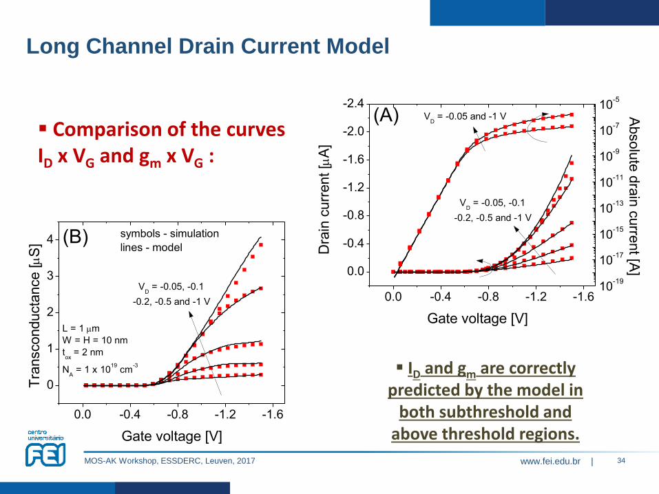
Long Channel Drain Current Model
▪ Comparison of the curves ID x VG and gm x VG :
▪ ID and gm are correctly predicted by the model in
both subthreshold and above threshold regions.
0.0 -0.4 -0.8 -1.2 -1.6
0.0
-0.4
-0.8
-1.2
-1.6
-2.0
-2.4
0.0 -0.4 -0.8 -1.2 -1.6
0
1
2
3
4V
D = -0.05 and -1 V A
bsolu
te d
rain
curre
nt [A
]
Dra
in c
urr
ent [
A]
Gate voltage [V]
L = 1 m
W = H = 10 nm
tox
= 2 nm
NA = 1 x 10
19 cm
-3
symbols - simulation
lines - model
VD = -0.05, -0.1
-0.2, -0.5 and -1 V
(A)
10-19
10-17
10-15
10-13
10-11
10-9
10-7
10-5
(B)
VD = -0.05, -0.1
-0.2, -0.5 and -1 V
Tra
nsconducta
nce [S
]
Gate voltage [V]
0.0 -0.4 -0.8 -1.2 -1.6
0.0
-0.4
-0.8
-1.2
-1.6
-2.0
-2.4
0.0 -0.4 -0.8 -1.2 -1.6
0
1
2
3
4V
D = -0.05 and -1 V A
bsolu
te d
rain
curre
nt [A
]
Dra
in c
urr
ent [
A]
Gate voltage [V]
L = 1 m
W = H = 10 nm
tox
= 2 nm
NA = 1 x 10
19 cm
-3
symbols - simulation
lines - model
VD = -0.05, -0.1
-0.2, -0.5 and -1 V
(A)
10-19
10-17
10-15
10-13
10-11
10-9
10-7
10-5
(B)
VD = -0.05, -0.1
-0.2, -0.5 and -1 V
Tra
nsconducta
nce [S
]
Gate voltage [V]

www.fei.edu.br | MOS-AK Workshop, ESSDERC, Leuven, 2017 35
Long Channel Drain Current Model
SBMicro 2012 - 27th Symposium on Microelectronics Technology and Devices
▪ Comparison of the curves ID x VD and gD x VD :
▪ The dependence on VD is also adequately
modeled
0.0 -0.4 -0.8 -1.2 -1.6
10-9
10-8
10-7
10-6
10-5
0.0 -0.4 -0.8 -1.2 -1.6
0.0
-0.5
-1.0
-1.5
-2.0(B)(A)
VGT
= -0.2, -0.4,
-0.6, -0.8 and -1 V
Dra
in c
onducta
nce [S
]
Drain voltage [V]
L = 1 m
tox
= 2 nm
W = H = 10 nm
NA = 1 x 10
19 cm
-3
Dra
in c
urr
ent [
A]
Drain voltage [V]
symbols - simulation
lines - model VGT
= -0.2, -0.4,
-0.6, -0.8 and -1 V
0.0 -0.4 -0.8 -1.2 -1.6
10-9
10-8
10-7
10-6
10-5
0.0 -0.4 -0.8 -1.2 -1.6
0.0
-0.5
-1.0
-1.5
-2.0(B)(A)
VGT
= -0.2, -0.4,
-0.6, -0.8 and -1 V
Dra
in c
onducta
nce [S
]
Drain voltage [V]
L = 1 m
tox
= 2 nm
W = H = 10 nm
NA = 1 x 10
19 cm
-3
Dra
in c
urr
ent [
A]
Drain voltage [V]
symbols - simulation
lines - model VGT
= -0.2, -0.4,
-0.6, -0.8 and -1 V

www.fei.edu.br | MOS-AK Workshop, ESSDERC, Leuven, 2017 36
Short Channel Effects
▪ To obtain an analytical expression for SCE, the 3D Poisson equation must be solved:
which is given by:
Si
ANq
dy
d
dz
d
dx
d
ε
ΦΦΦ2
2
2
2
2
2
▪ Using the superposition principle, the solution of the 2D Poisson equation can be added to the solution of the 3D Laplace equation for the minimum potential:
0ΦΦΦ2
2
2
2
2
2
dy
d
dz
d
dx
d
)/sinh(
)/)sinh(()/sinh(Φ minmin
min
L
yLUyV
ymin is point of the minimum potential given by:
)/exp(
)/exp(ln
2min
LUV
VLUy
is the characteristic length

www.fei.edu.br | MOS-AK Workshop, ESSDERC, Leuven, 2017 37
Short Channel Effects
where:
▪ The minimum potential in the channel is obtained by:
)/sinh(
)/)sinh(()/sinh(Φ minmin
min
L
yLUyV
)/exp(
)/exp(ln
2min
LUV
VLUy
▪ To calculate the drain current with the short channel effects correction:
12
2
2
1 2
11
2
14
12
oxSi
ox
ox
oxSi
t
WtW
2
22
14
oxSi
ox
ox
oxSi
t
HtH
and
min GG VV

www.fei.edu.br | MOS-AK Workshop, ESSDERC, Leuven, 2017 38
Short Channel Effects
▪min represents the variation of the minimum potential in the channel:
-0.6 -0.4 -0.2 0.0 0.2 0.4 0.6
-0.2
-0.1
0.0
0.1
0.2
0.3
0.4
0.5
0.6 VG = 1.2 V
VG = 0.4 V
C
hannel pote
ntial [V
]
y/L
L = 20 nm
L = 1 m
VG = 0 V
variation of the
minimum potential

www.fei.edu.br | MOS-AK Workshop, ESSDERC, Leuven, 2017 39
Short Channel Effects
▪ Comparison of the curves ID x VG and gm x VG for a device with L = 40 nm:
▪ ID and gm are correctly predicted by the model in
both subthreshold and above threshold regions.
0.0 -0.4 -0.8 -1.22
0
-2
-4
-6
-8
-10
-12
0.0 -0.4 -0.8 -1.2
0
5
10
15
20
Dra
in c
urr
ent [
A]
Gate voltage [V]
10-19
10-17
10-15
10-13
10-11
10-9
10-7
10-5
VD = -0.05, -0.1
-0.2 and -0.5 V
VD = -0.05 and -0.5 V
Absolu
te d
rain
curre
nt [A
]
symbols - simulation
lines - model
VD = -0.05, -0.1
-0.2 and -0.5 V
L = 40 nm
W = H = 10 nm
tox
= 2 nm
NA = 1 x 10
19 cm
-3
Tra
nsconducta
nce [S
]
Gate voltage [V]
(A) (B)

www.fei.edu.br | MOS-AK Workshop, ESSDERC, Leuven, 2017 40
Short Channel Effects
▪ The dependence on VD is also adequately
modeled
0.0 -0.4 -0.8 -1.2
0
-2
-4
-6
-8
-10
-12
0.0 -0.4 -0.8 -1.2
10-7
10-6
10-5
10-4
VGT
= -0.2, -0.4,
and -0.6 V
Dra
in c
urr
ent [
A]
Drain voltage [V]
L = 40 nm
W = H = 10 nm
tox
= 2 nm
NA = 1 x 10
19 cm
-3
symbols - simulation
lines - model
VGT
= -0.2, -0.4,
and -0.6 V
Dra
in c
onducta
nce [S
]
Drain voltage [V]
(A) (B)
0.0 -0.4 -0.8 -1.2
0
-2
-4
-6
-8
-10
-12
0.0 -0.4 -0.8 -1.2
10-7
10-6
10-5
10-4
VGT
= -0.2, -0.4,
and -0.6 V
Dra
in c
urr
ent [
A]
Drain voltage [V]
L = 40 nm
W = H = 10 nm
tox
= 2 nm
NA = 1 x 10
19 cm
-3
symbols - simulation
lines - model
VGT
= -0.2, -0.4,
and -0.6 V
Dra
in c
onducta
nce [S
]
Drain voltage [V]
(A) (B)
▪ Comparison of the curves ID x VD and gD x VD for a device with L = 40 nm:

www.fei.edu.br | MOS-AK Workshop, ESSDERC, Leuven, 2017 41
Short Channel Effects
▪ Comparison of the curve gm/ID x |ID|:
▪ The plateau in the weak inversion regime is inversely proportional to the subthreshoold slope
10-12
10-11
10-10
10-9
10-8
10-7
10-6
10-5
0
-10
-20
-30
-40
lines - model
symbols - simulation
W = H = 10 nm
tox
= 2 nm
NA = 1 x 10
19 cm
-3
VD = -0.05
and -0.5 V
L = 40 nm
VD = -0.05
and -0.5 V
gm/I
D [
V-1]
Absolute drain current [A]
L = 1 m
www.fei.edu.br | MOS-AK Workshop, ESSDERC, Leuven, 2017
0
25
50
75
100
-1.2 -0.8 -0.4 0.0 0.4 0.8
0
40
80
120
Dra
in c
urre
nt [A
]
Dra
in c
urr
en
t [
A]
symbols - experimental
lines - model
T = 300, 360
and 420 K
T = 300, 360
and 420 K
10-18
10-14
10-10
10-6
ND = 1 x 10
19 cm
-3
EOT = 1.5 nm
W = 20 nm
H = 12 nm
L = 30 nm
VD = 40 mV
50 fins
Tra
nsco
nd
ucta
nce
[S
]
Gate voltage [V]
T = 300, 360
and 420 K
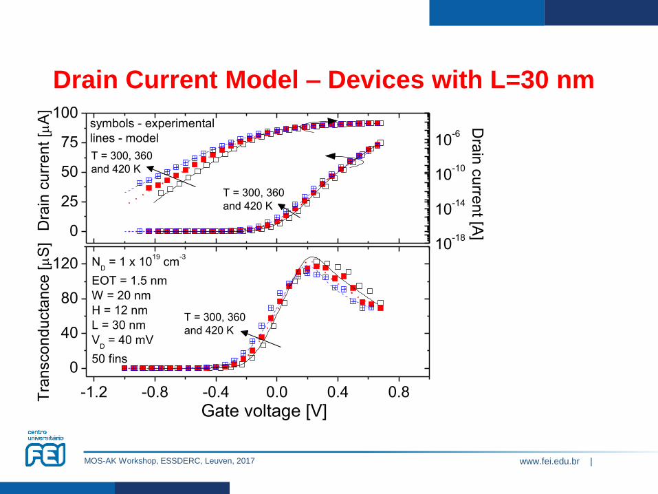
Drain Current Model – Devices with L=30 nm

www.fei.edu.br | MOS-AK Workshop, ESSDERC, Leuven, 2017
0.0 0.2 0.4 0.6 0.8 1.0
0
200
400
600
800 V
GT = 0.6 V
VGT
= 0.4 V
VGT
= 0.2 V
H = 10 nm
W = 20 nm
L = 30 nm
EOT = 1.5 nm
ND = 1 x 10
19 cm
-3
symbols - experimental
lines - model
Dra
in c
urr
ent [
A]
Drain voltage [V]
, T = 300 K
, T = 420 K
TREVISOLI, R.. D ; DORIA, R. T. ; DE SOUZA, M. ; DAS, S. ; FERAIN, I. ; PAVANELLO, M. A. . Surface
Potential-Based Drain Current Analytical Model for Triple-Gate Junctionless Nanowire Transistors. IEEE
Transactions on Electron Devices, v. 59, p. 3510-3518, 2012.
Drain Current Model – Devices with L=30 nm

www.fei.edu.br | MOS-AK Workshop, ESSDERC, Leuven, 2017 44
Long Channel Drain Current Model
▪ Relation between depletion charge and electric field:
Substrate Bias Influence
MOS capacitor:
SideplSDS εNqE /Φ ,
DeploxFBGdeplS Q)CVV( ,Φ a = Si q ND (2Heff + WFin)2
)(22
2
2
22, FBG
oxoxox
FBGdeplS VVCCC
VV
aaa
)(
2ε
ε
ε
ε
ε2
BSFBs
D
Si
ox
BoxSi
ox
BoxSiFineff VV
Nq
ttHH
)( BSFBsBoxFinFinDSi VVCHWNqQ
This approximation neglects the
cross-dependence between the gate
and the substrate biases on the
channel potential.

www.fei.edu.br | MOS-AK Workshop, ESSDERC, Leuven, 2017
0.0
0.1
0.2
0.3
-0.5 0.0 0.5 1.0 1.5
0
1
2
3
4
5 Dra
in c
urre
nt [A
]D
rain
curre
nt [A
]L = 1 m
Dra
in c
urr
ent [
A]
tox
= 2 nm
H = 10 nm
W = 10 nm
ND = 1 x 10
19 cm
-3
VBS
= -40, -20,
0, 20 e 40 V
Dra
in c
urr
ent [
A]
Gate Voltage [V]
VBS
= -40, -20,
0, 20 e 40 V
Symbols - Simulations
Lines - Model
L = 30 nm
10-14
10-11
10-8
10-5
10-15
10-12
10-9
10-6
TREVISOLI, Renan Doria ; DORIA, Rodrigo Trevisoli ; DE SOUZA, Michelly ; PAVANELLO, Marcelo
A. . Substrate Bias Influence on the Operation of Junctionless Nanowire Transistors. IEEE Transactions on
Electron Devices, v. 61, p. 1575-1582, 2014.

www.fei.edu.br | MOS-AK Workshop, ESSDERC, Leuven, 2017
Introduction & Motivation
Compact Modeling
Conclusion
The Junctionless Nanowire Transistor
Outline
Static Drain Current Model
Dynamic Model

www.fei.edu.br | MOS-AK Workshop, ESSDERC, Leuven, 2017
TREVISOLI, RENAN ; Doria, Rodrigo Trevisoli ; DE SOUZA, Michelly ; BARRAUD, SYLVAIN ; VINET, MAUD ;
Pavanello, Marcelo Antonio . Analytical Model for the Dynamic Behavior of Triple-Gate Junctionless Nanowire
Transistors. IEEE TRANSACTIONS ON ELECTRON DEVICES, v. 63, p. 856-863, 2016.

www.fei.edu.br | MOS-AK Workshop, ESSDERC, Leuven, 2017 48
Dynamic Model - Formulation
oxGSGFBBoxSBBFBsFinFinDC )CVyVV(V)CV(VHWqNQ ),(ΦΦ
Fixed
Charges
Substrate induced
Charges
Gate induced
Charges
▪ Conduction charge density per unit of length:
Gate
Substrate
N+ Si

www.fei.edu.br | MOS-AK Workshop, ESSDERC, Leuven, 2017 49
Dynamic Model - Formulation
▪ Total Conduction charge at the channel:
D
S
V
V
C
D
L
Ct dVyQI
dyQQ2
0
)(3
3
,
3
,
2,
,
DCSC
Dox
Q
Q
CC
Dox
t QQIC
dQQIC
QDC
SC
▪ Integrating the conduction charge density:
Charges density at
source-side
Charges density at drain-side
QG = Qt – L(qNDWH – CBox(VFBs – VB + SB)))
▪ Total charge at the gate:
ox
DCSC
DC
LI
2
)(2
,
2
,
www.fei.edu.br | MOS-AK Workshop, ESSDERC, Leuven, 2017 50
Dynamic Model - Formulation
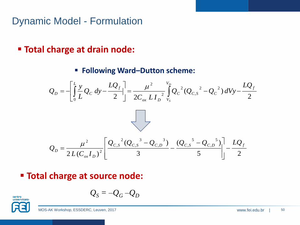
▪ Total charge at drain node:
▪ Following Ward–Dutton scheme:
QS = –QG –QD
▪ Total charge at source node:
D
S
V
V
f
CSCC
Dox
Lf
CD
LQdVyQQQ
ILC
LQdyQ
L
yQ
2)(
22
22
,
2
2
2
0
25
)(
3
)(
)(2
5
,
5
,
3
,
3
,
2
,
2
2fDCSCDCSCSC
Dox
D
LQQQQQQ
ICLQ

www.fei.edu.br | MOS-AK Workshop, ESSDERC, Leuven, 2017 51
Dynamic Model - Formulation
▪ Substituting the drain current into the charges equation:
QS = –QG –QD
f
DCSC
DCDCSCSC
G LQQQ
QQQQLQ
)(
)(
3
2
,,
2
,,,
2
,
2)2(15
)3642(22
,,,
2
,
3
,
2
,,,
2
,
3
, f
DCDCSCSC
DCDCSCDCSCSC
D
LQ
QQQQ
QQQQQQLQ
All charges are written in terms of the charge densities at source- and drain-side of the channel

www.fei.edu.br | MOS-AK Workshop, ESSDERC, Leuven, 2017 52
Dynamic Model - Formulation
▪ Transcapacitances:The transcapacitances are obtained by the node
charges derivatives:
2
,,
2
,,,
2
,
,,
,,,
2
,,
2
,,,
2
,
,,
,,,
)(
2
3
2
)(
2
3
2
DCSC
DCDCSCSC
DCSC
SCDC
k
DC
DCSC
DCDCSCSC
DCSC
DCSC
k
SC
k
G
QQQQ
V
QL
QQQQ
V
QL
V
Q
3
,
2
,,
2
,,
3
,
2
,,
2
,,
3
,,
3
,
2
,,
2
,,
3
,
2
,,
2
,,
3
,,
33
983
15
2
33
3
15
4
DCDCSCSCDCSC
DCSCSCDCDC
k
DC
DCDCSCSCDCSC
DCSCSCDCSC
k
SC
k
D
QQQQQQ
QQQQQ
V
QL
QQQQQQ
QQQQQ
V
QL
V
Q
k
D
k
G
k
S
V
Q
V
Q
V
Q
Box
k
SB
k
Box
k
GS
k
G
k
C CVV
VC
V
VyV
V
V
V
Q
Φ),(Φ
As the surface potentials are obtained analytically, their
derivatives are also analytical
All the transcapacitances are written in terms of QC
Cjk = – ∂Qj/∂Vk
www.fei.edu.br | MOS-AK Workshop, ESSDERC, Leuven, 2017 53
Dynamic Model - Formulation
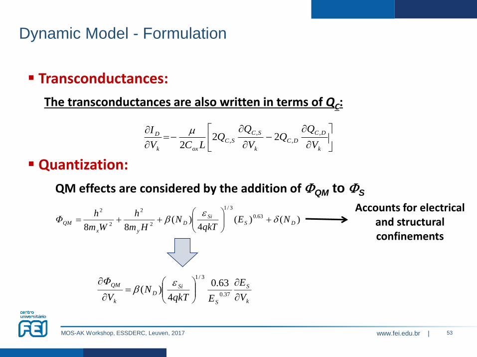
▪ Transconductances:
The transconductances are also written in terms of QC:
k
DC
DC
k
SC
SC
oxk
D
V
V
LCV
I ,
,
,
, 222
▪ Quantization:
QM effects are considered by the addition of QM to S
)()(4
)(88
63.0
3/1
2
2
2
2
DS
Si
D
yx
QM NEqkT
NHm
h
Wm
hΦ
Accounts for electrical and structural confinements
k
S
S
Si
D
k
QM
V
E
EqkTN
V
Φ
37.0
3/1
63.0
4)(

www.fei.edu.br | MOS-AK Workshop, ESSDERC, Leuven, 2017 54
Model Derivation
▪ Short-Channel Effects:
SCE effects are considered by the addition of the minimum
potential variation to VG
U and V are the surface potential at drain- and source-
sides of the channel
)/sinh(
)/)sinh(()/sinh(Φ minmin
min
L
yLUyV
)/exp(
)/exp(ln
2min
LUV
VLUy

www.fei.edu.br | MOS-AK Workshop, ESSDERC, Leuven, 2017
Dynamic Model – Comparison against 3D simulations
0 1 2 3
-0.5
0.0
0.5
1.0
-0.5 0.0 0.5 1.0 1.5 2.0
-6
-3
0
3
6
Ch
arg
e [
fC]
Gate voltage [V]
QG
QS
QD
tBox
= 100 nm
ND = 10
19 cm
-3
W = 10 nm
H = 10 nm
EOT = 2 nm
L = 1 m
VDS
= 1 V
Lines - Model
Symbols - Simulation
gDD
= dID/dV
D
gDS
= dID/dV
S
Co
nd
ucta
nce
s [S
]
Gate voltage [V]
tBox
= 100 nm
ND = 10
19 cm
-3
W = 10 nm
H = 10 nm
EOT = 2 nm
L = 1 m
VDS
= 1 V
gDG
= dID/dV
G

www.fei.edu.br | MOS-AK Workshop, ESSDERC, Leuven, 2017
Dynamic Model – Comparison against 3D simulations
0.0
0.2
0.4
0.6
0.0
0.2
0.4
0.0 0.5 1.0 1.5 2.0 2.5
0.00
0.02
0.04
0.06
CSD
CGDC
DS
Ca
pa
cita
nce
s [fF
]
CGG
, CGD
,CDS
,CSD
ND = 1 x 10
19 cm
-3
W = 10 nm
H = 10 nm
tox
= 2 nm
CGS
,CSG
, CDG
L = 1 m
VDS
= 1 V
tBox
= 10 nm
Lines - Model
Symbols - Simulation
CGB
, CSB
, CDB
CGG
CGS
CSG
CDG
Ca
pa
cita
nce
s [fF
]
CDB
CSB
CGB
Ca
pa
cita
nce
s [fF
]
Gate voltage [V]

www.fei.edu.br | MOS-AK Workshop, ESSDERC, Leuven, 2017
Dynamic Model – Comparison against 3D simulations
0 1 2
0.0
0.1
0.2
0.3
0.4
0.5
0.6
0.7
CGD
CGS
VDS
= 1 V
L = 1 m
Ca
pacitances [fF
]
Gate voltage [V]
Symbols - Simulation
Lines - Model
ND = 10
19 cm
-3
tBox
= 10 nm
W = 15 nm
H = 10 nm
tox
= 2 nm
VBS
= 2, 0
and -2 V
CGG

www.fei.edu.br | MOS-AK Workshop, ESSDERC, Leuven, 2017
Dynamic Model – Comparison against 3D simulations
0.00
0.01
0.02
0 1 20.00
0.01
0.02
W = 10 nmCGD
CGS
Capacitances [fF
] Dashed lines - Model neglecting SCEs
Solid lines - Model including SCEs
Symbols - Simulations
ND = 1 x 10
19 cm
-3
tBox
= 100 nm
H = 10 nm
tox
= 2 nm
L = 30 nm
VDS
= 0.5 V
CGG
W = 20 nm
CGD
CGS
CGG
Capacitances [fF
]
Gate voltage [V]
www.fei.edu.br | MOS-AK Workshop, ESSDERC, Leuven, 2017
Dynamic Model – Comparison against 3D simulations
0.0
0.1
0.2
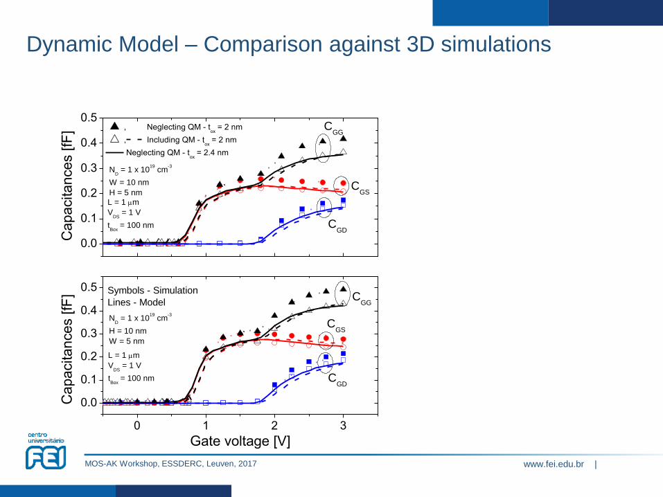
0.3
0.4
0.5
0 1 2 3
0.0
0.1
0.2
0.3
0.4
0.5
CGG
CGD
Ca
pa
cita
nce
s [fF
]
L = 1 m
VDS
= 1 V
tBox
= 100 nm
ND = 1 x 10
19 cm
-3
W = 10 nm
H = 5 nm
, Neglecting QM - tox
= 2 nm
, Including QM - tox
= 2 nm
Neglecting QM - tox
= 2.4 nm
CGS
CGG
CGS
CGD
Ca
pa
cita
nce
s [fF
]
Gate voltage [V]
Symbols - Simulation
Lines - Model
ND = 1 x 10
19 cm
-3
H = 10 nm
W = 5 nm
L = 1 m
VDS
= 1 V
tBox
= 100 nm

www.fei.edu.br | MOS-AK Workshop, ESSDERC, Leuven, 2017
Dynamic Model – Comparison against 3D simulations
0.0
0.20.4
0.60.8
1.01.2
0.0
0.4
0.8
1.2
1.6
2.0
0.0
0.2
0.4
0.6
0.8
1.0
1.2
0 1 2
0.0
0.1
0.2
0.3
0.4
0.5
0.6
W = 5, 20 and 50 nm
CGG
CGS
CGD
Ca
pa
cita
nce
s [fF
]
ND = 1 x 10
19 cm
-3
Symbols - Simulation
Lines - Model
tox = 2 nm
H = 10 nm
L = 1 m
VDS
= 1 V
tox = 2 nm
W = 10 nm
L = 1 m
VDS
= 1 V
H = 5, 20 and 50 nm
CGG
CGS
CGD
Ca
pa
cita
nce
s [fF
]N
D = 1 x 10
19 cm
-3
Symbols - Simulation
Lines - Model
(D)
(C)
(B)
CGG
CGS
CGD
Ca
pa
cita
nce
s [fF
]
Opened symbols - tox
= 1 nm
Closed symbols - tox
= 3 nm
ND = 1 x 10
19 cm
-3
W = 10 nm
H = 10 nm
L = 1 m
VDS
= 1 V
(A)
VDS
= 1 V
tox = 2 nm
W = 10 nm
H = 10 nm
L = 1 m
CGG
CGS
CGD
Ca
pa
cita
nce
s [fF
]
Gate voltage [V]
ND = 0.5, 2 and 3 x10
19 cm
-3
Symbols - Simulation
Lines - Model

www.fei.edu.br | MOS-AK Workshop, ESSDERC, Leuven, 2017
Dynamic Model – Comparison against Experimental data
0.0
0.2
0.4
0.6
-0.8 -0.4 0.0 0.4 0.8 1.2
0.0
0.2
0.4
0.6
0.8
CGS
Ca
pa
cita
nce
s [
pF
]
tBox
= 145 nm
VDS
= 0 V
VBS
= 0 V
EOT = 1.5 nm
H = 9 nm
L = 10 mOpened Symbols, dashed lines - Wmask
= 40 nm
Closed Symbols, solid lines - Wmask
= 20 nm
CGG
CGG
VBS
= -10,0, 10,
20 and 30 V
Ca
pa
cita
nce
s [
pF
]
Gate voltage [V]
EOT = 1.5 nm
Wmask
= 40 nm
H = 9 nm
L = 10 m tBox
= 145 nm
VDS
= 0 V
Symbols - Experimental
Lines - Model
TREVISOLI, RENAN ; Doria, Rodrigo Trevisoli ; DE SOUZA, Michelly ; BARRAUD, SYLVAIN ; VINET, MAUD ;
Pavanello, Marcelo Antonio . Analytical Model for the Dynamic Behavior of Triple-Gate Junctionless Nanowire
Transistors. IEEE TRANSACTIONS ON ELECTRON DEVICES, v. 63, p. 856-863, 2016.

www.fei.edu.br | MOS-AK Workshop, ESSDERC, Leuven, 2017
Introduction & Motivation
Compact Modeling
Conclusion
The Junctionless Nanowire Transistor
Outline
Static Drain Current Model
Dynamic Model

www.fei.edu.br | MOS-AK Workshop, ESSDERC, Leuven, 2017
•The Junctionless Nanowire Transistor is an interesting alternative for MOSFET
downscaling with respect to IM nanowires.
• Smaller IOFF and higher ION/IOFF at similar L (down to 10 nm).
•The analytical models presented show good agreement with experimental and
simulated data.
• Accounted for terminal voltages variations;
• Symmetric in the vicinity of VDS=0 V;
• Transconductances and transcapacitances.
Conclusion

www.fei.edu.br | MOS-AK Workshop, ESSDERC, Leuven, 2017
• Transfer the models to VERILOG-A
• Compact modeling of Low Frequency Noise
Tasks Ongoing
www.fei.edu.br | MOS-AK Workshop, ESSDERC, Leuven, 2017
Acknowledgements
Jean-Pierre Colinge
Olivier Faynot
Maud Vinet
Sylvain Barraud
Antonio CerdeiraMichelly de Souza
Rodrigo Doria
Renan Trevisoli
Genaro Mariniello
Bruna Cardoso Paz
Flávio Bergamaschi
Claudio Vilela Moreira

www.fei.edu.br | MOS-AK Workshop, ESSDERC, Leuven, 2017
Acknowledgements


![[Chapter III] Basic Knowledge of Discrete Semiconductor ......transistors (IGBTs) Power transistors (2SAxx,2SBxx,2SCxx,2SDxx, TTAxx,TTBxx,TTCxx,TTDxx) Types of Transistors Transistors](https://img.pdfslide.us/doc/110x75/5e766014341a1a707d5f4c34/chapter-iii-basic-knowledge-of-discrete-semiconductor-transistors-igbts.jpg)