Embed Size (px)
Citation preview
1
Static CMOS Circuits
2Ankur Agarwal
Static CMOS Circuits
In Static CMOS circuits with n inputs, 2n transistors are needed.
nMOS block is a dual of the pMOS block. What ever is in series in nMOS, appears in
parallel in pMOS and vice versa. CMOS gates consume power only during the
transition of inputs.
3Ankur Agarwal
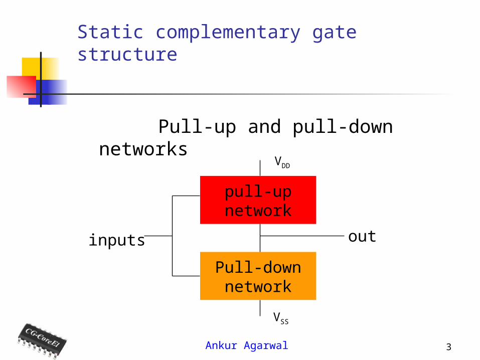
Static complementary gate structure
Pull-up and pull-down networks
pull-upnetwork
Pull-downnetwork
VDD
VSS
outinputs
4Ankur Agarwal
Pull-up/pull-down network design
Pull-up and pull-down networks are duals.
To design one gate, first design one network, then compute dual to get other network.

5Ankur Agarwal
Static CMOS Circuits
Static CMOS Logic Structure Logic Gates – Inverter, NAND and NOR Complex Structures AOI/OAI Structures Stick Diagrams Layouts
6Ankur Agarwal
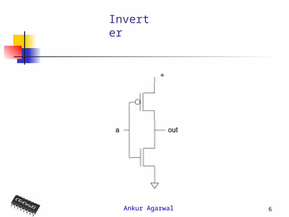
Inverter
7Ankur Agarwal
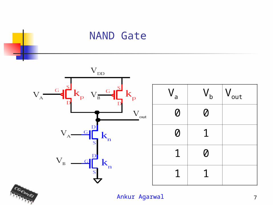
NAND Gate
Va Vb Vout
0 0
0 1
1 0
1 1
8Ankur Agarwal
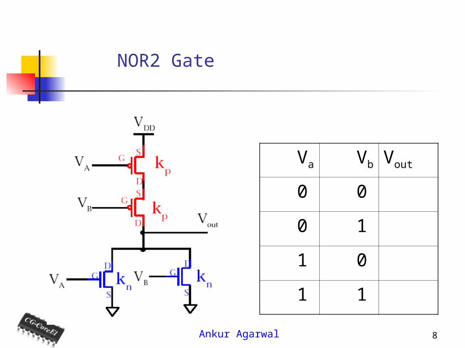
NOR2 Gate
Va Vb Vout
0 0
0 1
1 0
1 1
9Ankur Agarwal
Static CMOS Circuits
Static CMOS Logic Structure Logic Gates – Inverter, NAND and NOR Complex Structures AOI/OAI Structures Stick Diagrams Layouts
10Ankur Agarwal
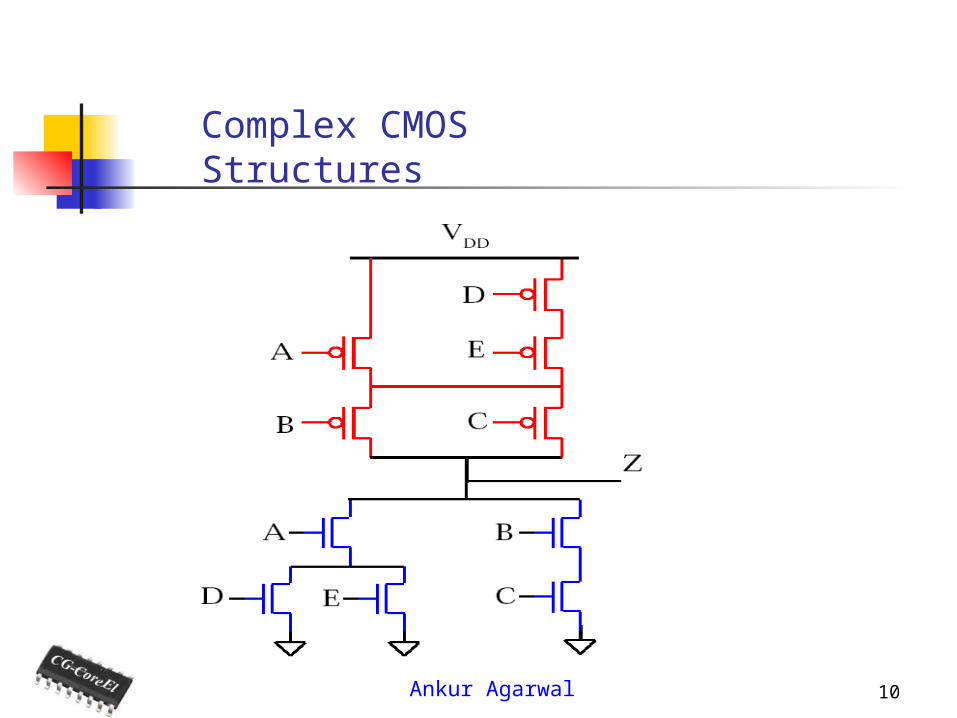
Complex CMOS Structures
11Ankur Agarwal
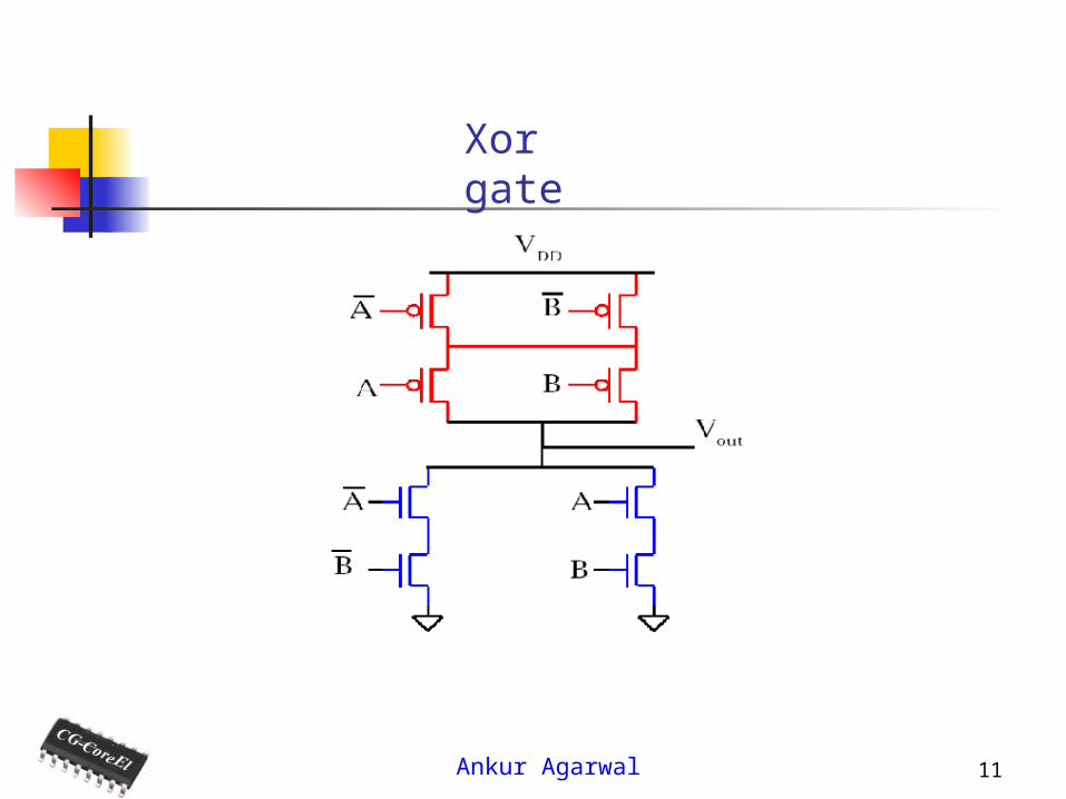
Xor gate
12Ankur Agarwal
Static CMOS Circuits
Static CMOS Logic Structure Logic Gates – Inverter, NAND and NOR Complex Structures AOI/OAI Structures Stick Diagrams Layouts
13Ankur Agarwal
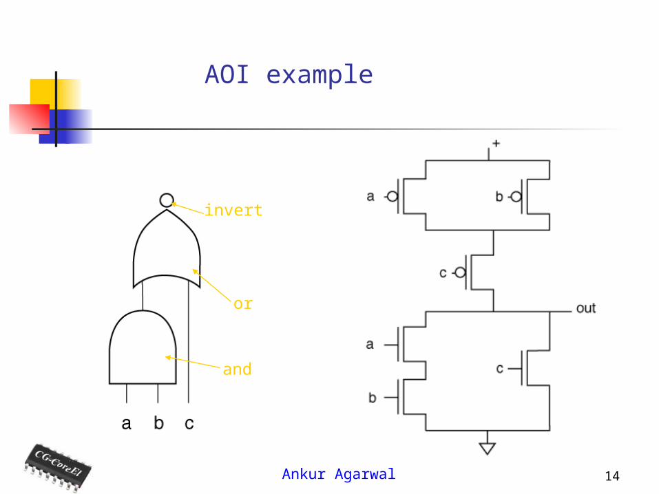
AOI/OAI gates
AOI = and/or/invert; OAI = or/and/invert. Implement larger functions. Pull-up and pull-down networks are compact:
smaller area, higher speed than NAND/NOR network equivalents.
14Ankur Agarwal
AOI example
and
or
invert
15Ankur Agarwal
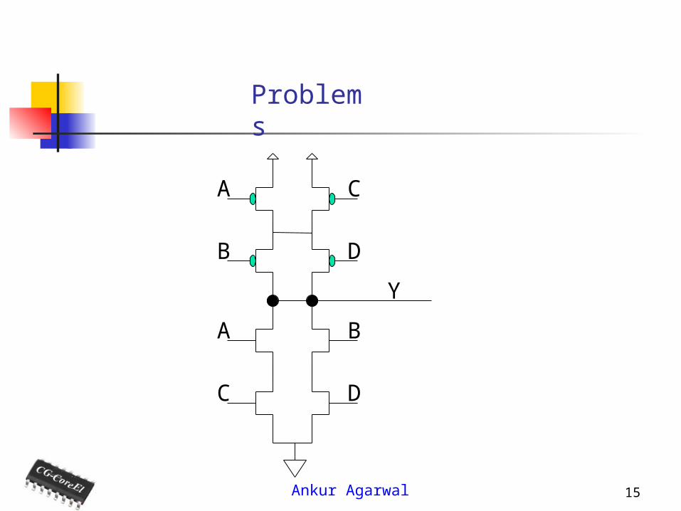
Problems
A
A
B
C
C
B
D
D
Y
16Ankur Agarwal
Problems
Design a CMOS circuit to implement the logic Y = A'B' + B'C + C'A
Make a 2 input CMOS XOR gate to implement Y = A B.
CMOS XOR and XNOR gates are similar. Just one of the input pairs (A and A' are reversed).
17Ankur Agarwal
Static CMOS Circuits
Static CMOS Logic Structure Logic Gates – Inverter, NAND and NOR Complex Structures AOI/OAI Structures Stick Diagrams Layouts
18Ankur Agarwal
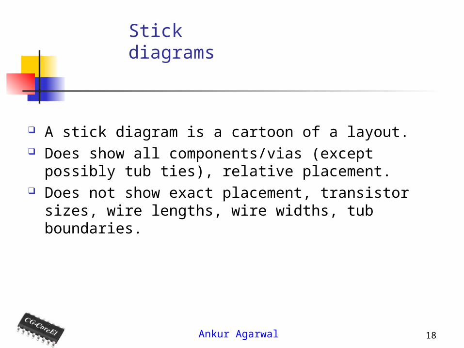
Stick diagrams
A stick diagram is a cartoon of a layout. Does show all components/vias (except possibly
tub ties), relative placement. Does not show exact placement, transistor sizes,
wire lengths, wire widths, tub boundaries.
19Ankur Agarwal
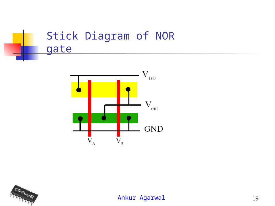
Stick Diagram of NOR gate
20Ankur Agarwal
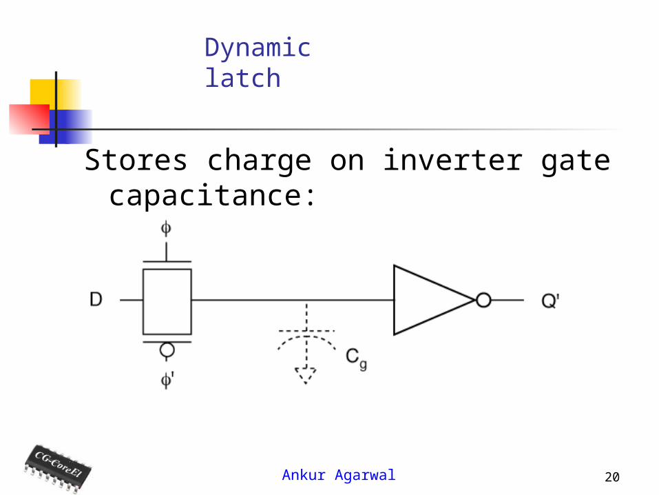
Dynamic latch
Stores charge on inverter gate capacitance:
21Ankur Agarwal
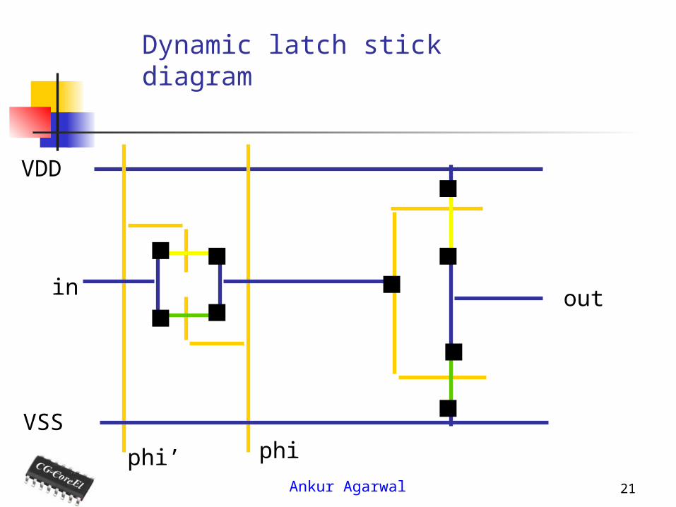
Dynamic latch stick diagram
VDD
in
VSSphiphi’
out

22Ankur Agarwal
Static CMOS Circuits
Static CMOS Logic Structure Logic Gates – Inverter, NAND and NOR Complex Structures AOI/OAI Structures Stick Diagrams Layouts
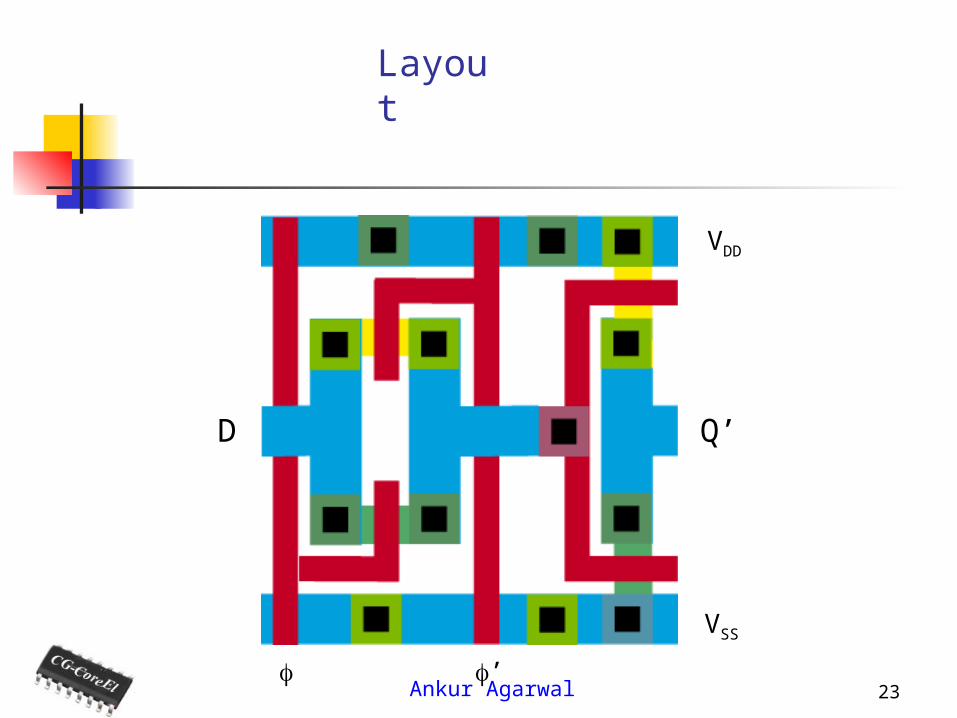
23Ankur Agarwal
Layout
D Q’
VDD
VSS
’
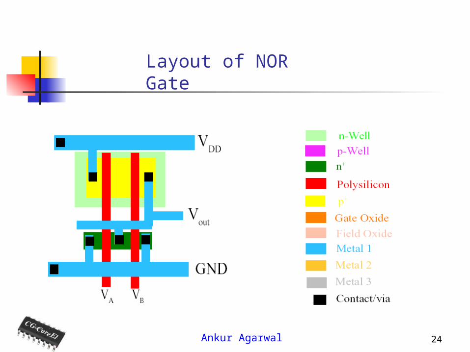
24Ankur Agarwal
Layout of NOR Gate
25Ankur Agarwal
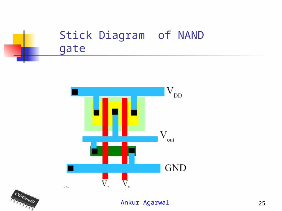
Stick Diagram of NAND gate