Embed Size (px)
Citation preview

JESD204C v2.0
LogiCORE IP Product Guide
Vivado Design SuitePG242 October 4, 2017
JESD204C v2.0 www.xilinx.com 2PG242 October 4, 2017
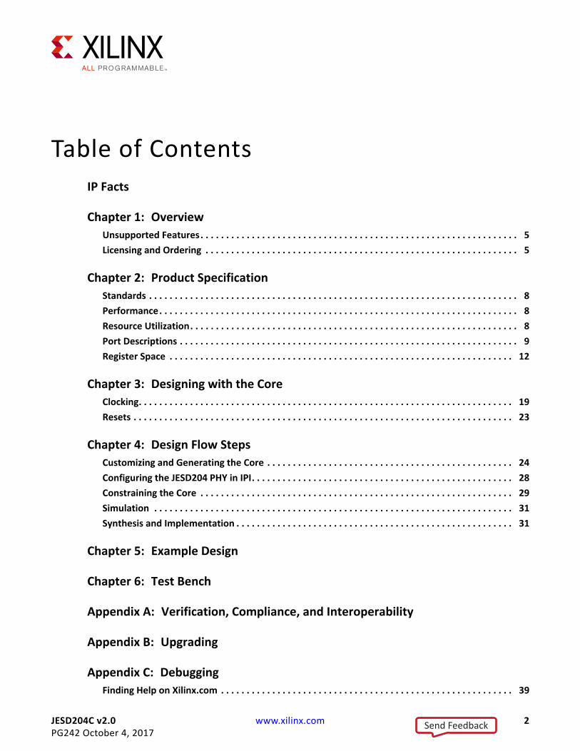
Table of Contents
IP Facts
Chapter 1: Overview
Unsupported Features. . . . . . . . . . . . . . . . . . . . . . . . . . . . . . . . . . . . . . . . . . . . . . . . . . . . . . . . . . . . . . 5
Licensing and Ordering . . . . . . . . . . . . . . . . . . . . . . . . . . . . . . . . . . . . . . . . . . . . . . . . . . . . . . . . . . . . . 5
Chapter 2: Product Specification
Standards . . . . . . . . . . . . . . . . . . . . . . . . . . . . . . . . . . . . . . . . . . . . . . . . . . . . . . . . . . . . . . . . . . . . . . . . 8
Performance. . . . . . . . . . . . . . . . . . . . . . . . . . . . . . . . . . . . . . . . . . . . . . . . . . . . . . . . . . . . . . . . . . . . . . 8
Resource Utilization. . . . . . . . . . . . . . . . . . . . . . . . . . . . . . . . . . . . . . . . . . . . . . . . . . . . . . . . . . . . . . . . 8
Port Descriptions . . . . . . . . . . . . . . . . . . . . . . . . . . . . . . . . . . . . . . . . . . . . . . . . . . . . . . . . . . . . . . . . . . 9
Register Space . . . . . . . . . . . . . . . . . . . . . . . . . . . . . . . . . . . . . . . . . . . . . . . . . . . . . . . . . . . . . . . . . . . 12
Chapter 3: Designing with the Core
Clocking. . . . . . . . . . . . . . . . . . . . . . . . . . . . . . . . . . . . . . . . . . . . . . . . . . . . . . . . . . . . . . . . . . . . . . . . . 19
Resets . . . . . . . . . . . . . . . . . . . . . . . . . . . . . . . . . . . . . . . . . . . . . . . . . . . . . . . . . . . . . . . . . . . . . . . . . . 23
Chapter 4: Design Flow Steps
Customizing and Generating the Core . . . . . . . . . . . . . . . . . . . . . . . . . . . . . . . . . . . . . . . . . . . . . . . . 24
Configuring the JESD204 PHY in IPI. . . . . . . . . . . . . . . . . . . . . . . . . . . . . . . . . . . . . . . . . . . . . . . . . . . 28
Constraining the Core . . . . . . . . . . . . . . . . . . . . . . . . . . . . . . . . . . . . . . . . . . . . . . . . . . . . . . . . . . . . . 29
Simulation . . . . . . . . . . . . . . . . . . . . . . . . . . . . . . . . . . . . . . . . . . . . . . . . . . . . . . . . . . . . . . . . . . . . . . 31
Synthesis and Implementation . . . . . . . . . . . . . . . . . . . . . . . . . . . . . . . . . . . . . . . . . . . . . . . . . . . . . . 31
Chapter 5: Example Design
Chapter 6: Test Bench
Appendix A: Verification, Compliance, and Interoperability
Appendix B: Upgrading
Appendix C: Debugging
Finding Help on Xilinx.com . . . . . . . . . . . . . . . . . . . . . . . . . . . . . . . . . . . . . . . . . . . . . . . . . . . . . . . . . 39
Send Feedback
JESD204C v2.0 www.xilinx.com 3PG242 October 4, 2017
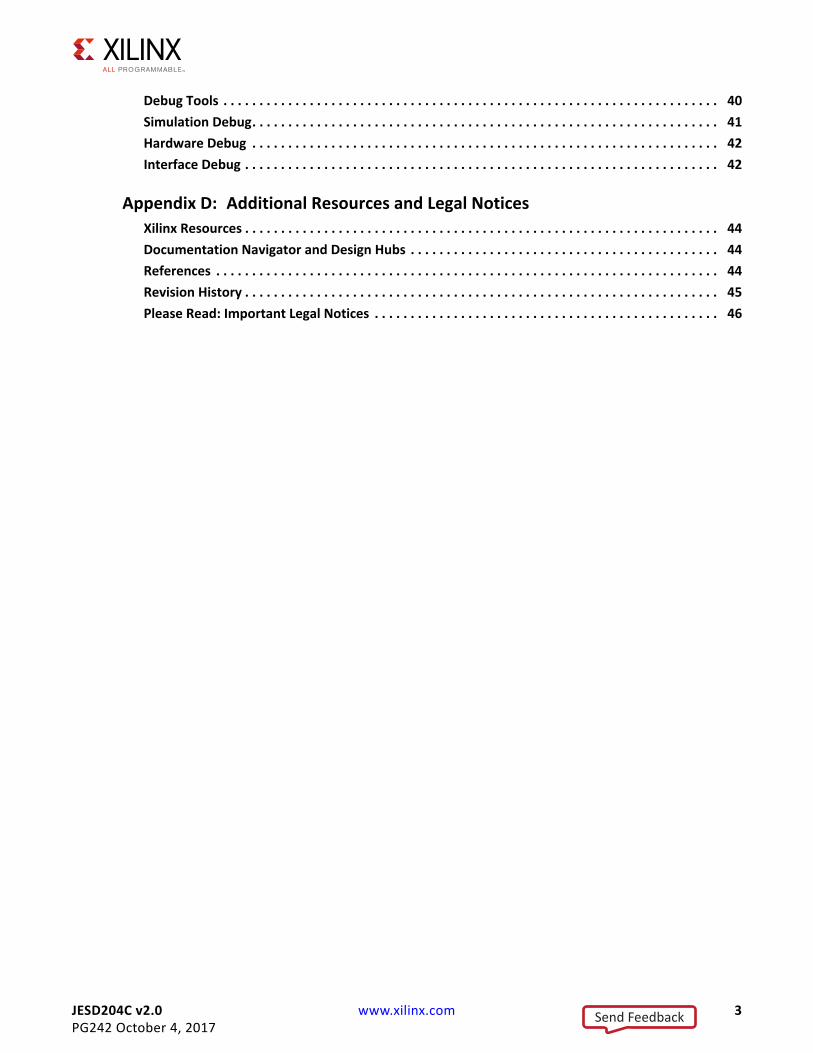
Debug Tools . . . . . . . . . . . . . . . . . . . . . . . . . . . . . . . . . . . . . . . . . . . . . . . . . . . . . . . . . . . . . . . . . . . . . 40
Simulation Debug. . . . . . . . . . . . . . . . . . . . . . . . . . . . . . . . . . . . . . . . . . . . . . . . . . . . . . . . . . . . . . . . . 41
Hardware Debug . . . . . . . . . . . . . . . . . . . . . . . . . . . . . . . . . . . . . . . . . . . . . . . . . . . . . . . . . . . . . . . . . 42
Interface Debug . . . . . . . . . . . . . . . . . . . . . . . . . . . . . . . . . . . . . . . . . . . . . . . . . . . . . . . . . . . . . . . . . . 42
Appendix D: Additional Resources and Legal Notices
Xilinx Resources . . . . . . . . . . . . . . . . . . . . . . . . . . . . . . . . . . . . . . . . . . . . . . . . . . . . . . . . . . . . . . . . . . 44
Documentation Navigator and Design Hubs . . . . . . . . . . . . . . . . . . . . . . . . . . . . . . . . . . . . . . . . . . . 44
References . . . . . . . . . . . . . . . . . . . . . . . . . . . . . . . . . . . . . . . . . . . . . . . . . . . . . . . . . . . . . . . . . . . . . . 44
Revision History . . . . . . . . . . . . . . . . . . . . . . . . . . . . . . . . . . . . . . . . . . . . . . . . . . . . . . . . . . . . . . . . . . 45
Please Read: Important Legal Notices . . . . . . . . . . . . . . . . . . . . . . . . . . . . . . . . . . . . . . . . . . . . . . . . 46
Send Feedback
JESD204C v2.0 www.xilinx.com 4PG242 October 4, 2017 Product Specification
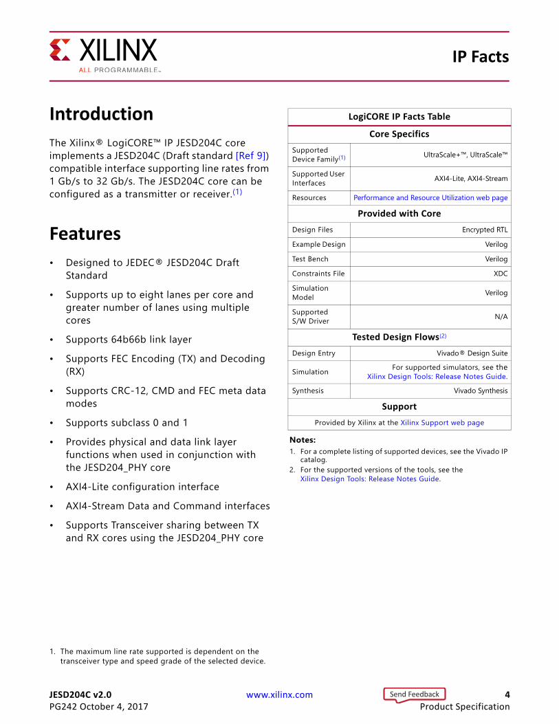
Introduction
The Xilinx® LogiCORE™ IP JESD204C core implements a JESD204C (Draft standard [Ref 9]) compatible interface supporting line rates from 1 Gb/s to 32 Gb/s. The JESD204C core can be configured as a transmitter or receiver.(1)
Features
• Designed to JEDEC® JESD204C Draft Standard
• Supports up to eight lanes per core and greater number of lanes using multiple cores
• Supports 64b66b link layer• Supports FEC Encoding (TX) and Decoding
(RX)• Supports CRC-12, CMD and FEC meta data
modes• Supports subclass 0 and 1• Provides physical and data link layer
functions when used in conjunction with the JESD204_PHY core
• AXI4-Lite configuration interface• AXI4-Stream Data and Command interfaces• Supports Transceiver sharing between TX
and RX cores using the JESD204_PHY core
1. The maximum line rate supported is dependent on the transceiver type and speed grade of the selected device.
IP Facts
LogiCORE IP Facts Table
Core Specifics
Supported Device Family(1) UltraScale+™, UltraScale™
Supported User Interfaces AXI4-Lite, AXI4-Stream
Resources Performance and Resource Utilization web page
Provided with Core
Design Files Encrypted RTL
Example Design Verilog
Test Bench Verilog
Constraints File XDC
Simulation Model Verilog
Supported S/W Driver N/A
Tested Design Flows(2)
Design Entry Vivado® Design Suite
Simulation For supported simulators, see theXilinx Design Tools: Release Notes Guide.
Synthesis Vivado Synthesis
Support
Provided by Xilinx at the Xilinx Support web page
Notes: 1. For a complete listing of supported devices, see the Vivado IP
catalog.2. For the supported versions of the tools, see the
Xilinx Design Tools: Release Notes Guide.
Send Feedback
JESD204C v2.0 www.xilinx.com 5PG242 October 4, 2017
Chapter 1
OverviewThe LogiCORE™ IP JESD204C core implements a JESD204C link layer. When used in conjunction with the LogiCORE™ IP JESD204_PHY core (to provide the physical layer), a JESD204C system can be created supporting line rates between 1 and 32 Gb/s on 1 to 8 lanes using GTYE4 and GTYE3 (UltraScale+ and UltraScale) transceivers. See the device data sheets for maximum line rates supported by each device and family. The JESD204C core can be configured as transmit or receive and multiple cores can be used to realize links requiring more than eight lanes.
The JESD204C core is delivered by using the Xilinx® Vivado® Design Suite. In addition, an example design is provided in Verilog.
Unsupported FeaturesSample data mapping/demapping is not provided by the core, because of the requirement that it be customized for different converter devices. For more information see applicable converter datasheets.
Licensing and Ordering
License Checkers
If the IP requires a license key, the key must be verified. The Vivado design tools have several license checkpoints for gating licensed IP through the flow. If the license check succeeds, the IP can continue generation. Otherwise, generation halts with error. License checkpoints are enforced by the following tools:
• Vivado synthesis• Vivado implementation• write_bitstream (Tcl command)
IMPORTANT: IP license level is ignored at checkpoints. The test confirms a valid license exists. It does not check IP license level.
Send Feedback
JESD204C v2.0 www.xilinx.com 6PG242 October 4, 2017
Chapter 1: Overview
License Type
This Xilinx LogiCORE IP module is provided under the terms of the Xilinx Core License Agreement. The module is shipped as part of the Vivado Design Suite. For full access to all core functionalities in simulation and in hardware, you must purchase a license for the core. Contact your local Xilinx sales representative for information about pricing and availability.
For more information, visit the JESD204 product web page.
Information about other Xilinx LogiCORE IP modules is available at the Xilinx Intellectual Property page. For information on pricing and availability of other Xilinx LogiCORE IP modules and tools, contact your local Xilinx sales representative.
A free evaluation version of the core is provided with the Xilinx Vivado Design Suite which lets you assess the core functionality and demonstrates the various interfaces of the core in simulation. To access the evaluation version visit the JESD204 IP Evaluation page.
License Options
The JESD204C IP core license is provided as part of the JESD204 core License (no separate license is required). The JESD204 core license provides three options. After installing the Vivado Design Suite and the required IP Service Packs, choose a licensing option.
Simulation Only
The Simulation Only Evaluation license key is provided with the Xilinx Vivado Design Suite. This key lets you assess core functionality with either the example design provided with the JESD204C core, or alongside your own design and demonstrates the various interfaces to the core in simulation. (Functional simulation is supported by a dynamically generated HDL structural model.)
Full System Hardware Evaluation
The Full System Hardware Evaluation license is available at no cost and lets you fully integrate the core into an FPGA design, place-and-route the design, evaluate timing, and perform functional simulation of the JESD204C core using the example design and demonstration test bench provided with the core.
In addition, the license key lets you generate a bitstream from the placed and routed design, which can then be downloaded to a supported device and tested in hardware. The core can be tested in the target device for a limited time before timing out (ceasing to function), at which time it can be reactivated by reconfiguring the device.
Send Feedback
JESD204C v2.0 www.xilinx.com 7PG242 October 4, 2017
Chapter 1: Overview
Full
The Full license key is available when you purchase the core and provides full access to all core functionality both in simulation and in hardware, including:
• Gate-level functional simulation support• Back annotated gate-level simulation support• Functional simulation support • Full-implementation support including place and route and bitstream generation• Full functionality in the programmed device with no time-outs
Obtaining Your License Key
This section contains information about obtaining a simulation, full system hardware, and full license keys.
Simulation License
No action is required to obtain the Simulation Only Evaluation license key; it is provided by default with the Xilinx Vivado Design Suite.
Full System Hardware Evaluation License
To obtain a Full System Hardware Evaluation license, perform these steps:
1. Navigate to the JESD204 product page for this core.2. Click Evaluate.3. Follow the instructions on the page.
Obtaining a Full License
To obtain a Full license key, you must purchase a license for the core. After doing so, click the Access Core link on the xilinx.com IP core product page for further instructions.
Installing Your License File
The Simulation only Evaluation license key is provided with the Vivado Design Suite and does not require installation of an additional license file. For the Full System Hardware Evaluation license and the Full license, an email will be sent to you containing instructions for installing your license file. Additional details about IP license key installation can be found in the Vivado Design Suite Installation, Licensing and Release Notes document.
Send Feedback
JESD204C v2.0 www.xilinx.com 8PG242 October 4, 2017
Chapter 2
Product SpecificationThe JESD204C core is used in conjunction with the JESD204_PHY core to support the draft JESD204C physical layer link layer specification.
StandardsJEDEC® Serial interface for Data Converters JESD204C draft [Ref 9].
PerformanceFor details about performance, visit the Performance and Resource Utilization web page.
Resource UtilizationFor details about resource utilization, visit the Performance and Resource Utilization web page.
Send Feedback
JESD204C v2.0 www.xilinx.com 9PG242 October 4, 2017
Chapter 2: Product Specification
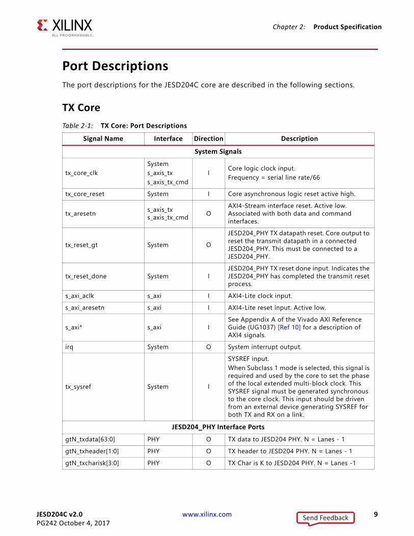
Port DescriptionsThe port descriptions for the JESD204C core are described in the following sections.
TX Core
Table 2‐1: TX Core: Port Descriptions
Signal Name Interface Direction Description
System Signals
tx_core_clkSystem s_axis_txs_axis_tx_cmd
I Core logic clock input.Frequency = serial line rate/66
tx_core_reset System I Core asynchronous logic reset active high.
tx_aresetn s_axis_tx s_axis_tx_cmd O
AXI4-Stream interface reset. Active low. Associated with both data and command interfaces.
tx_reset_gt System OJESD204_PHY TX datapath reset. Core output to reset the transmit datapath in a connected JESD204_PHY. This must be connected to a JESD204_PHY.
tx_reset_done System IJESD204_PHY TX reset done input. Indicates the JESD204_PHY has completed the transmit reset process.
s_axi_aclk s_axi I AXI4-Lite clock input.s_axi_aresetn s_axi I AXI4-Lite reset input. Active low.
s_axi* s_axi ISee Appendix A of the Vivado AXI Reference Guide (UG1037) [Ref 10] for a description of AXI4 signals.
irq System O System interrupt output.
tx_sysref System I
SYSREF input. When Subclass 1 mode is selected, this signal is required and used by the core to set the phase of the local extended multi-block clock. This SYSREF signal must be generated synchronous to the core clock. This input should be driven from an external device generating SYSREF for both TX and RX on a link.
JESD204_PHY Interface Ports
gtN_txdata[63:0] PHY O TX data to JESD204 PHY. N = Lanes - 1gtN_txheader[1:0] PHY O TX header to JESD204 PHY. N = Lanes - 1gtN_txcharisk[3:0] PHY O TX Char is K to JESD204 PHY. N = Lanes -1
Send Feedback
JESD204C v2.0 www.xilinx.com 10PG242 October 4, 2017
Chapter 2: Product Specification
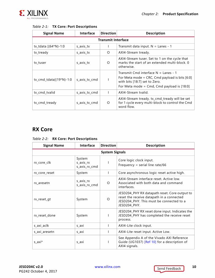
RX Core
Transmit Interface
tx_tdata [(64*N)-1:0 s_axis_tx I Transmit data input. N = Lanes - 1tx_tready s_axis_tx O AXI4-Stream tready.
tx_tuser s_axis_tx OAXI4-Stream tuser. Set to 1 on the cycle that marks the start of an extended multi-block. 0 otherwise.
tx_cmd_tdata[(19*N)-1:0 s_axis_tx_cmd I
Transmit Cmd interface N = Lanes - 1For Meta mode = CRC, Cmd payload is bits [6:0] with bits [18:7] set to Zero.For Meta mode = Cmd, Cmd payload is [18:0]
tx_cmd_tvalid s_axis_tx_cmd I AXI4-Stream tvalid.
tx_cmd_tready s_axis_tx_cmd OAXI4-Stream tready. tx_cmd_tready will be set for 1 cycle every multi-block to control the Cmd word flow.
Table 2‐2: RX Core: Port Descriptions
Signal Name Interface Direction Description
System Signals
rx_core_clkSystem s_axis_rx s_axis_rx_cmd
I Core logic clock input.Frequency = serial line rate/66
rx_core_reset System I Core asynchronous logic reset active high.
rx_aresetn s_axis_rx s_axis_rx_cmd O
AXI4-Stream interface reset. Active low. Associated with both data and command interfaces.
rx_reset_gt System OJESD204_PHY RX datapath reset. Core output to reset the receive datapath in a connected JESD204_PHY. This must be connected to a JESD204_PHY.
rx_reset_done System IJESD204_PHY RX reset done input. Indicates the JESD204_PHY has completed the receive reset process.
s_axi_aclk s_axi I AXI4-Lite clock input.s_axi_aresetn s_axi I AXI4-Lite reset input. Active Low.
s_axi* s_axi ISee Appendix A of the Vivado AXI Reference Guide (UG1037) [Ref 10] for a description of AXI4 signals.
Table 2‐1: TX Core: Port Descriptions
Signal Name Interface Direction Description
Send Feedback
JESD204C v2.0 www.xilinx.com 11PG242 October 4, 2017
Chapter 2: Product Specification
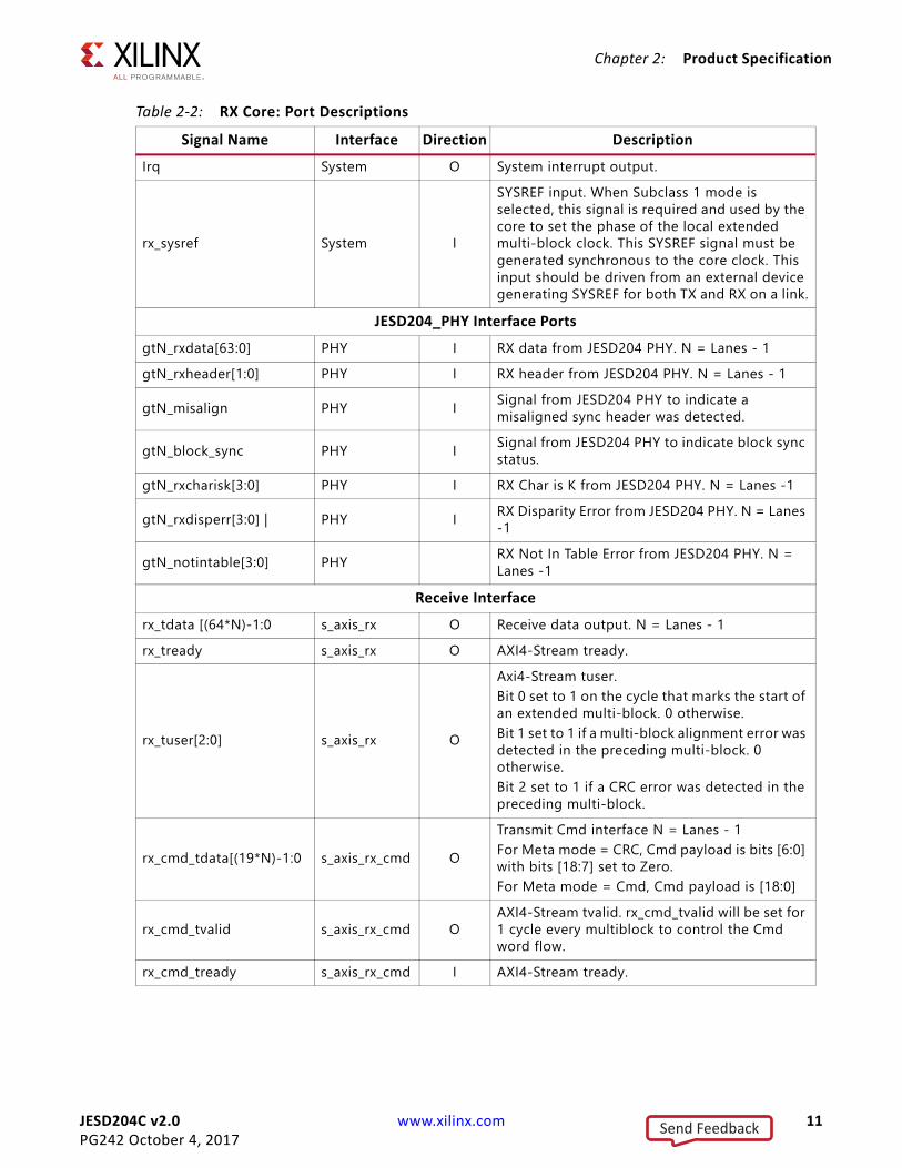
Irq System O System interrupt output.
rx_sysref System I
SYSREF input. When Subclass 1 mode is selected, this signal is required and used by the core to set the phase of the local extended multi-block clock. This SYSREF signal must be generated synchronous to the core clock. This input should be driven from an external device generating SYSREF for both TX and RX on a link.
JESD204_PHY Interface Ports
gtN_rxdata[63:0] PHY I RX data from JESD204 PHY. N = Lanes - 1gtN_rxheader[1:0] PHY I RX header from JESD204 PHY. N = Lanes - 1
gtN_misalign PHY I Signal from JESD204 PHY to indicate a misaligned sync header was detected.
gtN_block_sync PHY I Signal from JESD204 PHY to indicate block sync status.
gtN_rxcharisk[3:0] PHY I RX Char is K from JESD204 PHY. N = Lanes -1
gtN_rxdisperr[3:0] | PHY I RX Disparity Error from JESD204 PHY. N = Lanes -1
gtN_notintable[3:0] PHY RX Not In Table Error from JESD204 PHY. N = Lanes -1
Receive Interface
rx_tdata [(64*N)-1:0 s_axis_rx O Receive data output. N = Lanes - 1rx_tready s_axis_rx O AXI4-Stream tready.
rx_tuser[2:0] s_axis_rx O
Axi4-Stream tuser.Bit 0 set to 1 on the cycle that marks the start of an extended multi-block. 0 otherwise.Bit 1 set to 1 if a multi-block alignment error was detected in the preceding multi-block. 0 otherwise.Bit 2 set to 1 if a CRC error was detected in the preceding multi-block.
rx_cmd_tdata[(19*N)-1:0 s_axis_rx_cmd O
Transmit Cmd interface N = Lanes - 1For Meta mode = CRC, Cmd payload is bits [6:0] with bits [18:7] set to Zero.For Meta mode = Cmd, Cmd payload is [18:0]
rx_cmd_tvalid s_axis_rx_cmd OAXI4-Stream tvalid. rx_cmd_tvalid will be set for 1 cycle every multiblock to control the Cmd word flow.
rx_cmd_tready s_axis_rx_cmd I AXI4-Stream tready.
Table 2‐2: RX Core: Port Descriptions
Signal Name Interface Direction Description
Send Feedback
JESD204C v2.0 www.xilinx.com 12PG242 October 4, 2017
Chapter 2: Product Specification
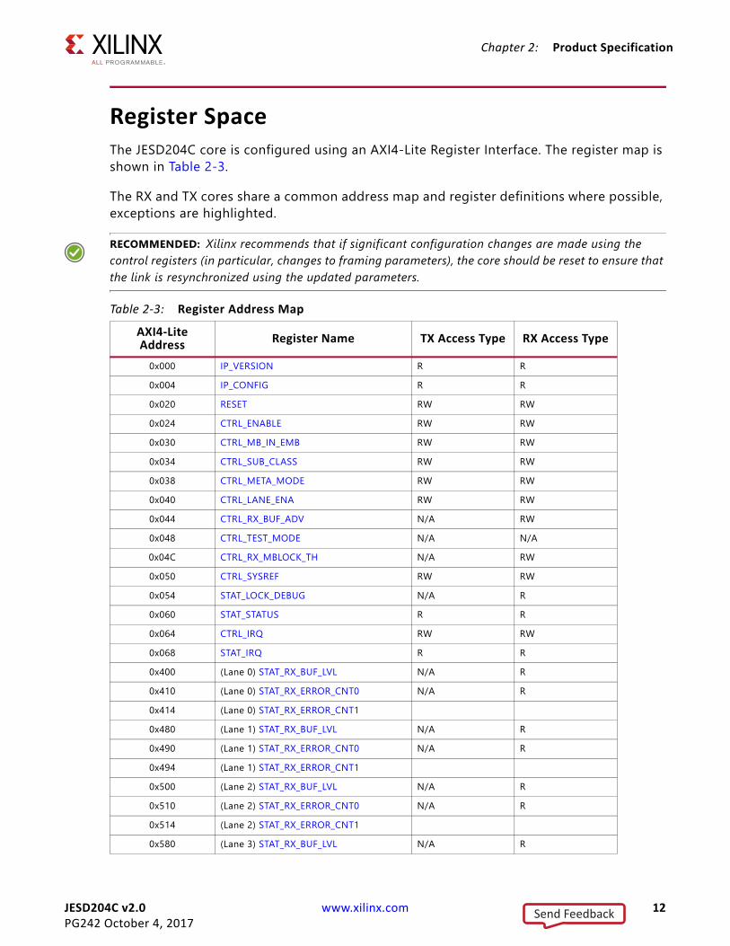
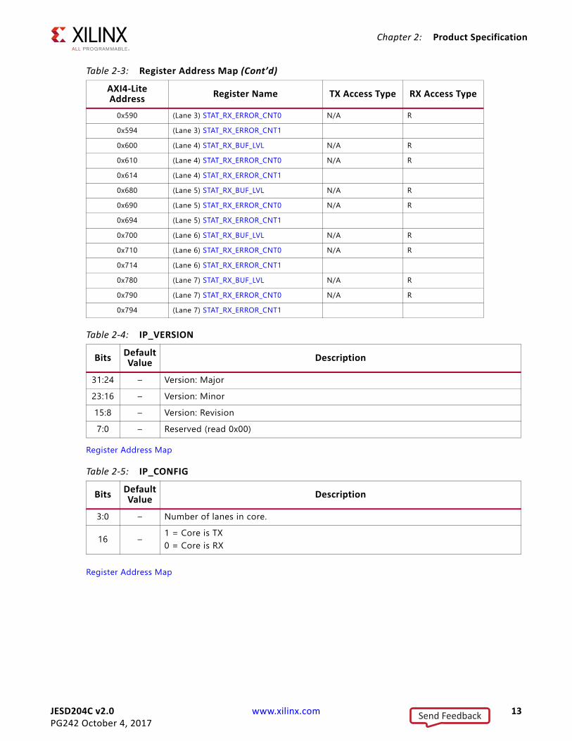
Register SpaceThe JESD204C core is configured using an AXI4-Lite Register Interface. The register map is shown in Table 2-3.
The RX and TX cores share a common address map and register definitions where possible, exceptions are highlighted.
RECOMMENDED: Xilinx recommends that if significant configuration changes are made using the control registers (in particular, changes to framing parameters), the core should be reset to ensure that the link is resynchronized using the updated parameters.
Table 2‐3: Register Address Map
AXI4-LiteAddress
Register Name TX Access Type RX Access Type
0x000 IP_VERSION R R
0x004 IP_CONFIG R R
0x020 RESET RW RW
0x024 CTRL_ENABLE RW RW
0x030 CTRL_MB_IN_EMB RW RW
0x034 CTRL_SUB_CLASS RW RW
0x038 CTRL_META_MODE RW RW
0x040 CTRL_LANE_ENA RW RW
0x044 CTRL_RX_BUF_ADV N/A RW
0x048 CTRL_TEST_MODE N/A N/A
0x04C CTRL_RX_MBLOCK_TH N/A RW
0x050 CTRL_SYSREF RW RW
0x054 STAT_LOCK_DEBUG N/A R
0x060 STAT_STATUS R R
0x064 CTRL_IRQ RW RW
0x068 STAT_IRQ R R
0x400 (Lane 0) STAT_RX_BUF_LVL N/A R
0x410 (Lane 0) STAT_RX_ERROR_CNT0 N/A R
0x414 (Lane 0) STAT_RX_ERROR_CNT1
0x480 (Lane 1) STAT_RX_BUF_LVL N/A R
0x490 (Lane 1) STAT_RX_ERROR_CNT0 N/A R
0x494 (Lane 1) STAT_RX_ERROR_CNT1
0x500 (Lane 2) STAT_RX_BUF_LVL N/A R
0x510 (Lane 2) STAT_RX_ERROR_CNT0 N/A R
0x514 (Lane 2) STAT_RX_ERROR_CNT1
0x580 (Lane 3) STAT_RX_BUF_LVL N/A R
Send Feedback
JESD204C v2.0 www.xilinx.com 13PG242 October 4, 2017
Chapter 2: Product Specification
Register Address Map
Register Address Map
0x590 (Lane 3) STAT_RX_ERROR_CNT0 N/A R
0x594 (Lane 3) STAT_RX_ERROR_CNT1
0x600 (Lane 4) STAT_RX_BUF_LVL N/A R
0x610 (Lane 4) STAT_RX_ERROR_CNT0 N/A R
0x614 (Lane 4) STAT_RX_ERROR_CNT1
0x680 (Lane 5) STAT_RX_BUF_LVL N/A R
0x690 (Lane 5) STAT_RX_ERROR_CNT0 N/A R
0x694 (Lane 5) STAT_RX_ERROR_CNT1
0x700 (Lane 6) STAT_RX_BUF_LVL N/A R
0x710 (Lane 6) STAT_RX_ERROR_CNT0 N/A R
0x714 (Lane 6) STAT_RX_ERROR_CNT1
0x780 (Lane 7) STAT_RX_BUF_LVL N/A R
0x790 (Lane 7) STAT_RX_ERROR_CNT0 N/A R
0x794 (Lane 7) STAT_RX_ERROR_CNT1
Table 2‐4: IP_VERSION
BitsDefaultValue Description
31:24 – Version: Major23:16 – Version: Minor15:8 – Version: Revision7:0 – Reserved (read 0x00)
Table 2‐5: IP_CONFIG
BitsDefaultValue
Description
3:0 – Number of lanes in core.
16 – 1 = Core is TX0 = Core is RX
Table 2‐3: Register Address Map (Cont’d)
AXI4-LiteAddress
Register Name TX Access Type RX Access Type
Send Feedback
JESD204C v2.0 www.xilinx.com 14PG242 October 4, 2017
Chapter 2: Product Specification
Register Address Map
Register Address Map
Register Address Map
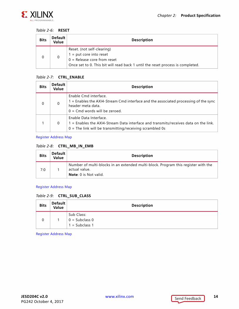
Table 2‐6: RESET
BitsDefault Value Description
0 0
Reset. (not self-clearing)1 = put core into reset0 = Release core from resetOnce set to 0. This bit will read back 1 until the reset process is completed.
Table 2‐7: CTRL_ENABLE
BitsDefaultValue Description
0 0
Enable Cmd interface.1 = Enables the AXI4-Stream Cmd interface and the associated processing of the sync header meta data.0 = Cmd words will be zeroed.
1 0Enable Data Interface.1 = Enables the AXI4-Stream Data interface and transmits/receives data on the link.0 = The link will be transmitting/receiving scrambled 0s
Table 2‐8: CTRL_MB_IN_EMB
BitsDefaultValue Description
7:0 1Number of multi-blocks in an extended multi-block. Program this register with the actual value. Note: 0 is Not valid.
Table 2‐9: CTRL_SUB_CLASS
BitsDefaultValue Description
0 1Sub Class:0 = Subclass 01 = Subclass 1
Send Feedback
JESD204C v2.0 www.xilinx.com 15PG242 October 4, 2017
Chapter 2: Product Specification
Register Address Map
Register Address Map
Register Address Map
Register Address Map
Register Address Map
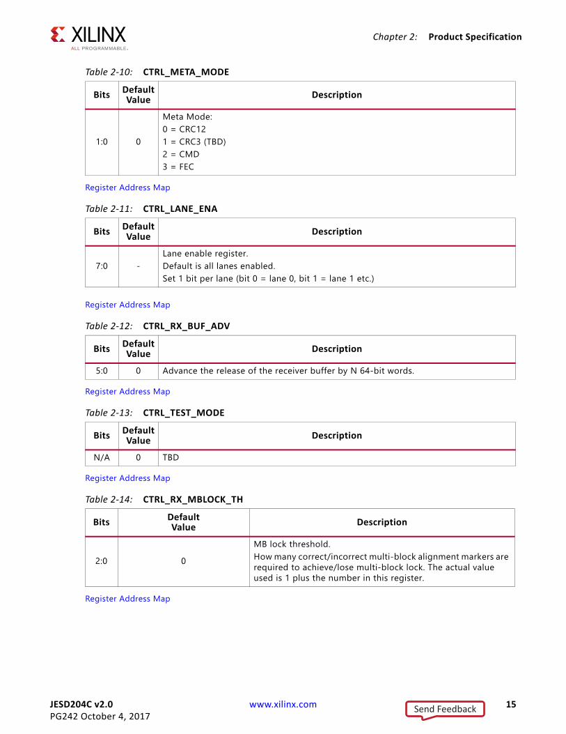
Table 2‐10: CTRL_META_MODE
BitsDefaultValue Description
1:0 0
Meta Mode:0 = CRC121 = CRC3 (TBD)2 = CMD3 = FEC
Table 2‐11: CTRL_LANE_ENA
BitsDefaultValue
Description
7:0 -Lane enable register. Default is all lanes enabled.Set 1 bit per lane (bit 0 = lane 0, bit 1 = lane 1 etc.)
Table 2‐12: CTRL_RX_BUF_ADV
BitsDefaultValue Description
5:0 0 Advance the release of the receiver buffer by N 64-bit words.
Table 2‐13: CTRL_TEST_MODE
BitsDefaultValue
Description
N/A 0 TBD
Table 2‐14: CTRL_RX_MBLOCK_TH
Bits DefaultValue
Description
2:0 0MB lock threshold.How many correct/incorrect multi-block alignment markers are required to achieve/lose multi-block lock. The actual value used is 1 plus the number in this register.
Send Feedback
JESD204C v2.0 www.xilinx.com 16PG242 October 4, 2017
Chapter 2: Product Specification
Register Address Map
Register Address Map
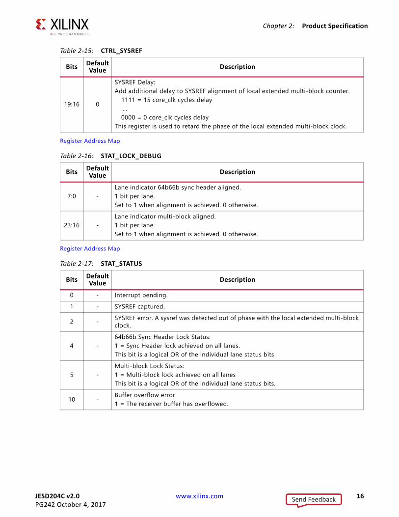
Table 2‐15: CTRL_SYSREF
BitsDefaultValue Description
19:16 0
SYSREF Delay:Add additional delay to SYSREF alignment of local extended multi-block counter.
1111 = 15 core_clk cycles delay....0000 = 0 core_clk cycles delay
This register is used to retard the phase of the local extended multi-block clock.
Table 2‐16: STAT_LOCK_DEBUG
BitsDefaultValue
Description
7:0 -Lane indicator 64b66b sync header aligned.1 bit per lane.Set to 1 when alignment is achieved. 0 otherwise.
23:16 -Lane indicator multi-block aligned.1 bit per lane.Set to 1 when alignment is achieved. 0 otherwise.
Table 2‐17: STAT_STATUS
Bits DefaultValue
Description
0 - Interrupt pending.1 - SYSREF captured.
2 - SYSREF error. A sysref was detected out of phase with the local extended multi-block clock.
4 -64b66b Sync Header Lock Status:1 = Sync Header lock achieved on all lanes.This bit is a logical OR of the individual lane status bits
5 -Multi-block Lock Status:1 = Multi-block lock achieved on all lanesThis bit is a logical OR of the individual lane status bits.
10 - Buffer overflow error.1 = The receiver buffer has overflowed.
Send Feedback
JESD204C v2.0 www.xilinx.com 17PG242 October 4, 2017
Chapter 2: Product Specification
Register Address Map
Register Address Map
Register Address Map
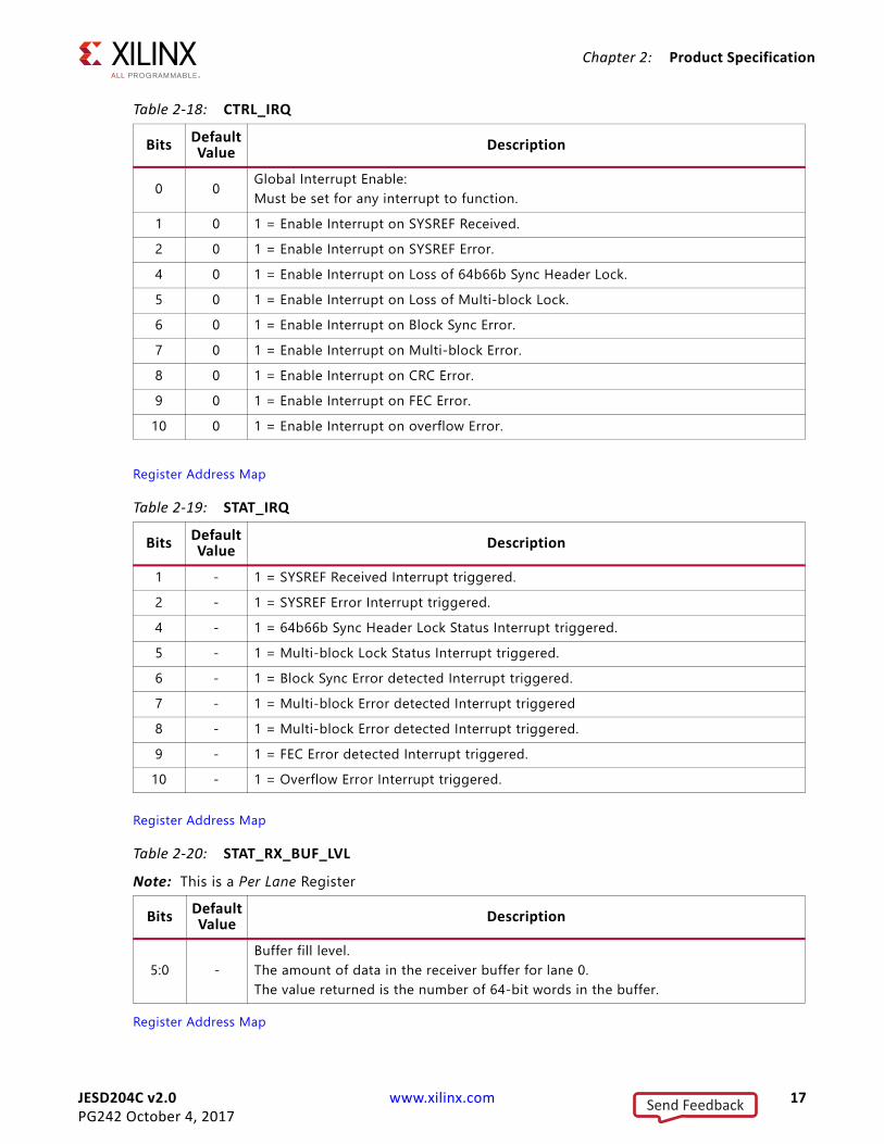
Table 2‐18: CTRL_IRQ
Bits Default Value
Description
0 0 Global Interrupt Enable:Must be set for any interrupt to function.
1 0 1 = Enable Interrupt on SYSREF Received.2 0 1 = Enable Interrupt on SYSREF Error.4 0 1 = Enable Interrupt on Loss of 64b66b Sync Header Lock.5 0 1 = Enable Interrupt on Loss of Multi-block Lock.6 0 1 = Enable Interrupt on Block Sync Error.7 0 1 = Enable Interrupt on Multi-block Error.8 0 1 = Enable Interrupt on CRC Error.9 0 1 = Enable Interrupt on FEC Error.
10 0 1 = Enable Interrupt on overflow Error.
Table 2‐19: STAT_IRQ
Bits DefaultValue
Description
1 - 1 = SYSREF Received Interrupt triggered.2 - 1 = SYSREF Error Interrupt triggered.4 - 1 = 64b66b Sync Header Lock Status Interrupt triggered.5 - 1 = Multi-block Lock Status Interrupt triggered.6 - 1 = Block Sync Error detected Interrupt triggered.7 - 1 = Multi-block Error detected Interrupt triggered8 - 1 = Multi-block Error detected Interrupt triggered.9 - 1 = FEC Error detected Interrupt triggered.
10 - 1 = Overflow Error Interrupt triggered.
Table 2‐20: STAT_RX_BUF_LVL
Note: This is a Per Lane Register
BitsDefault Value Description
5:0 -Buffer fill level.The amount of data in the receiver buffer for lane 0.The value returned is the number of 64-bit words in the buffer.
Send Feedback
JESD204C v2.0 www.xilinx.com 18PG242 October 4, 2017
Chapter 2: Product Specification
Register Address Map
Register Address Map
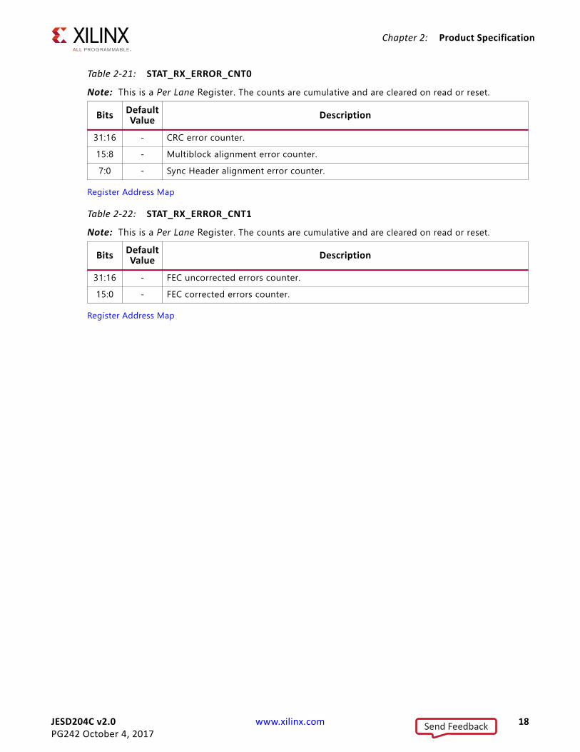
Table 2‐21: STAT_RX_ERROR_CNT0
Note: This is a Per Lane Register. The counts are cumulative and are cleared on read or reset.
Bits Default Value
Description
31:16 - CRC error counter.15:8 - Multiblock alignment error counter.7:0 - Sync Header alignment error counter.
Table 2‐22: STAT_RX_ERROR_CNT1
Note: This is a Per Lane Register. The counts are cumulative and are cleared on read or reset.
BitsDefault Value Description
31:16 - FEC uncorrected errors counter.15:0 - FEC corrected errors counter.
Send Feedback
JESD204C v2.0 www.xilinx.com 19PG242 October 4, 2017
Chapter 3
Designing with the CoreThis chapter provides a general description of how to use the JESD204C core in your designs and should be used in conjunction with Chapter 2, Product Specification, which describes specific core interfaces.
ClockingIMPORTANT: It is strongly recommended that you use one of the clocking schemes presented in this section. Use of alternative clocking schemes may lead to design failure.
The JESD204C specification [Ref 9] does not define specific serial line rates for any JESD204C link, but a valid range of line rates from 312.5 Mb/s to 32 Gb/s. The JESD204C core supports line rates from 1 Gb/s to 32 Gb/s (depending on the part and speed grade selection). In most instances, the serial line rate selection is governed by the specifications of the ADC/DAC Converter device(s) to which the core is interfaced. The required operating serial line rate directly relates to the clock rate at which the core logic operates (core clock); the serial line rate also governs the selection of the reference clock required by the transceiver(s).
Core Clock
The JESD204C core operates using a 64-bit (8-byte) datapath. The core clock frequency is always the line rate divided by 66. For example, for a serial line rate of 16.5 Gb/s, the core clock frequency is 250 MHz.
The AXI4-streaming RX / TX Data and Cmd interfaces operate at this core clock frequency. TX and RX core_clock should be used as the clock source for these interfaces.
Reference Clock
The GTY serial transceivers in the JESD204_PHY require a stable, low-jitter reference clock which has a device and speed grade-dependent range. In some circumstances, it can be advantageous to use the same clock frequency for both core clock and reference clock. However this might not always be practical. It is important to understand the limitations imposed on the reference clock and core clock, together with system-level implications such as the synchronous capture of SYSREF for Subclass 1.
Send Feedback
JESD204C v2.0 www.xilinx.com 20PG242 October 4, 2017
Chapter 3: Designing with the Core
AXI4-Lite Interface Clock
The JESD204C core is configured and monitored through an AXI4-Lite processor interface. The clock for this interface is separate and independent from the core and reference clocks.
DRP Clock
JESD204C system implementation requires the use of a JESD204 PHY core. The JESD204_PHY core must be supplied with a DRP clock (see JESD204 PHY LogiCORE IP Product Guide PG198 [Ref 11]).
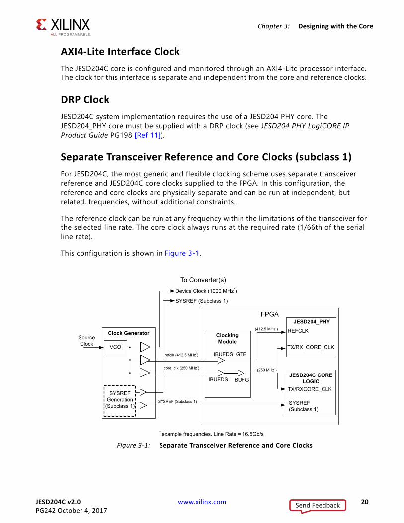
Separate Transceiver Reference and Core Clocks (subclass 1)
For JESD204C, the most generic and flexible clocking scheme uses separate transceiver reference and JESD204C core clocks supplied to the FPGA. In this configuration, the reference and core clocks are physically separate and can be run at independent, but related, frequencies, without additional constraints.
The reference clock can be run at any frequency within the limitations of the transceiver for the selected line rate. The core clock always runs at the required rate (1/66th of the serial line rate).
This configuration is shown in Figure 3-1.X-Ref Target - Figure 3-1
Figure 3‐1: Separate Transceiver Reference and Core Clocks
Clock Generator
VCO
Source Clock
To Converter(s)Device Clock (1000 MHz*)
SYSREF (Subclass 1)
refclk (412.5 MHz*)
core_clk (250 MHz*)
SYSREF (Subclass 1)
FPGA
(412.5 MHz*)
(250 MHz*)
Clocking Module
IBUFDS_GTE
IBUFDS BUFG
JESD204_PHYREFCLK
TX/RX_CORE_CLK
JESD204C CORE LOGIC
TX/RXCORE_CLK
SYSREF (Subclass 1)
* example frequencies. Line Rate = 16.5Gb/s
SYSREFGeneration
(Subclass 1)
Send Feedback
JESD204C v2.0 www.xilinx.com 21PG242 October 4, 2017
Chapter 3: Designing with the Core
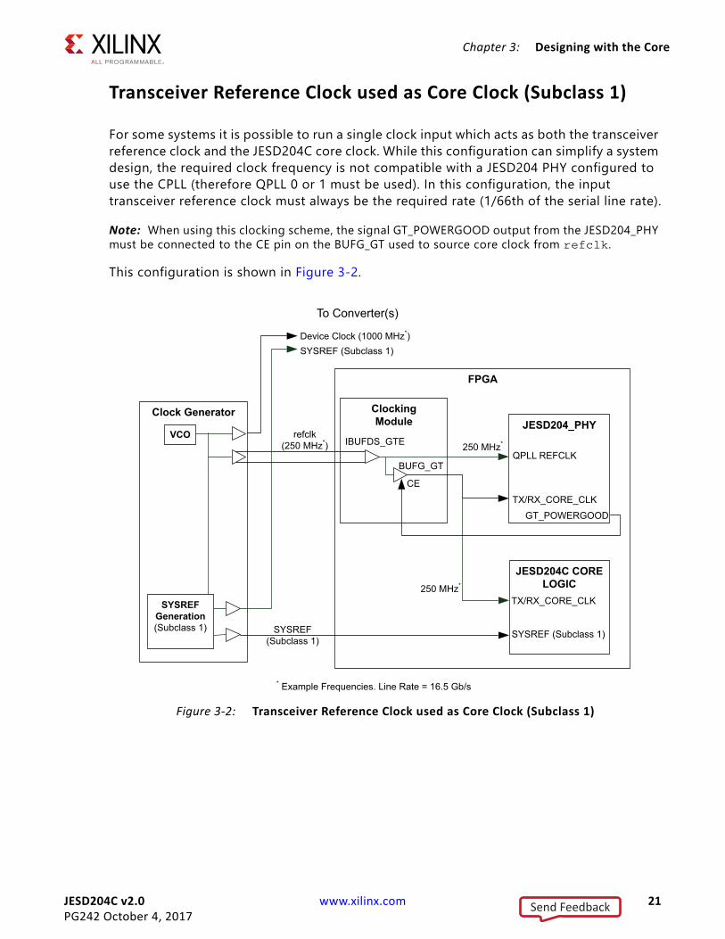
Transceiver Reference Clock used as Core Clock (Subclass 1)
For some systems it is possible to run a single clock input which acts as both the transceiver reference clock and the JESD204C core clock. While this configuration can simplify a system design, the required clock frequency is not compatible with a JESD204 PHY configured to use the CPLL (therefore QPLL 0 or 1 must be used). In this configuration, the input transceiver reference clock must always be the required rate (1/66th of the serial line rate).
Note: When using this clocking scheme, the signal GT_POWERGOOD output from the JESD204_PHY must be connected to the CE pin on the BUFG_GT used to source core clock from refclk.
This configuration is shown in Figure 3-2.X-Ref Target - Figure 3-2
Figure 3‐2: Transceiver Reference Clock used as Core Clock (Subclass 1)
FPGA
250 MHz*IBUFDS_GTEQPLL REFCLK
TX/RX_CORE_CLK
SYSREF (Subclass 1)
JESD204C CORE LOGIC
JESD204_PHYrefclk
(250 MHz*)
Clock Generator
VCO
SYSREFGeneration(Subclass 1) SYSREF
(Subclass 1)
SYSREF (Subclass 1)Device Clock (1000 MHz*)
ClockingModule
TX/RX_CORE_CLK
250 MHz*
BUFG_GT
To Converter(s)
* Example Frequencies. Line Rate = 16.5 Gb/s
GT_POWERGOOD
CE
Send Feedback
JESD204C v2.0 www.xilinx.com 22PG242 October 4, 2017
Chapter 3: Designing with the Core
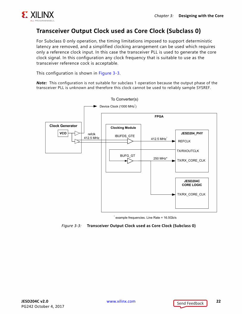
Transceiver Output Clock used as Core Clock (Subclass 0)
For Subclass 0 only operation, the timing limitations imposed to support deterministic latency are removed, and a simplified clocking arrangement can be used which requires only a reference clock input. In this case the transceiver PLL is used to generate the core clock signal. In this configuration any clock frequency that is suitable to use as the transceiver reference cock is acceptable.
This configuration is shown in Figure 3-3.
Note: This configuration is not suitable for subclass 1 operation because the output phase of the transceiver PLL is unknown and therefore this clock cannot be used to reliably sample SYSREF.X-Ref Target - Figure 3-3
Figure 3‐3: Transceiver Output Clock used as Core Clock (Subclass 0)
refclk412.5 MHz
FPGA
Clocking Module
IBUFDS_GTE
BUFG_GT
JESD204_PHY
REFCLK
TX/RX_CORE_CLK
TX/RX_CORE_CLK
JESD204CCORE LOGIC
TX/RXOUTCLK
250 MHz*
Clock Generator
VCO412.5 MHz*
Device Clock (1000 MHz*)
To Converter(s)
* example frequencies. Line Rate = 16.5Gb/s
Send Feedback
JESD204C v2.0 www.xilinx.com 23PG242 October 4, 2017
Chapter 3: Designing with the Core
Clocking Considerations
• Always refer to the device data sheet for the chosen part and speed grade to confirm which PLLs are available for a required line rate - PLL selection for a particular rate may not be arbitrary.
• The CPLL supports a maximum line rate in any device of 12.5 Gb/s.• If the CPLL is required, the transceiver reference clock cannot be used as the core clk
because the acceptable reference clock input frequencies to the CPLL do not cover the required Line Rate/66 ratio.
• For Line rates above 16.375G, ensure only port MGTREFCLK0 is used to drive QPLL0, and MGTREFCLK1 to drive QPLL1.
ResetsThe reset inputs and outputs on the JESD204C core are as shown in Table 3-1.
Table 3‐1: JESD204C Resets
Reset Description
tx/rx_core_reset This reset input is asynchronous and active high.This reset input will reset the JESD204C core logic but does not reset the AXI4-Lite register interface - so all programmed values will be maintained.
s_axi_aresetn This reset input must be synchronized with the AXI4-Lite interface clock.This reset input will reset the AXI4-Lite register interface.
tx/rx_reset_gt This reset output must be connected to the JESD204_PHY core. This signal is used to initiate a JESD204_PHY GT reset sequence.
tx/rx_reset_done This input must be connected to the JESD204_PHY core. This signal is used to hold the JESD204C core in reset until completion of the JESD204_PHY GT reset sequence.Note: A low input on this port will force the JESD204C core into a reset state.
tx/rx_aresetn This reset output is synchronous to tx/rx_core_clk.This output is an AXI4-Streaming interface reset signal to be used with the AXI4-streaming RX / TX Data and Cmd interfaces.
Send Feedback

JESD204C v2.0 www.xilinx.com 24PG242 October 4, 2017
Chapter 4
Design Flow StepsThis chapter describes customizing and generating the JESD204C core, constraining the core, and the simulation, synthesis and implementation steps that are specific to this IP core. More detailed information about the standard Vivado® design flows and the Vivado IP integrator can be found in the following Vivado Design Suite user guides:
• Vivado Design Suite User Guide: Designing IP Subsystems using IP Integrator (UG994) [Ref 1]
• Vivado Design Suite User Guide: Designing with IP (UG896) [Ref 2]• Vivado Design Suite User Guide: Getting Started (UG910) [Ref 3]• Vivado Design Suite User Guide: Logic Simulation (UG900) [Ref 4]
Customizing and Generating the CoreThis section includes information on using Xilinx tools to customize and generate the core in the Vivado Design Suite.
If you are customizing and generating the core in the IP integrator, see the Vivado Design Suite User Guide: Designing IP Subsystems using IP Integrator (UG994) [Ref 1] for detailed information. IP integrator might auto-compute certain configuration values when validating or generating the design. To check whether the values do change, see the description of the parameter in this chapter. To view the parameter value you can run the validate_bd_design command in the Tcl console.
You can customize the IP for use in your design by specifying values for the various parameters associated with the IP core using the following steps:
1. Select the IP from the Vivado IP catalog.2. Double-click the selected IP or select the Customize IP command from the toolbar or
right-click menu.
For details, see the Vivado Design Suite User Guide: Designing with IP (UG896) [Ref 2] and the Vivado Design Suite User Guide: Getting Started (UG910) [Ref 3].
Note: Figures in this chapter are illustrations of the JESD204C GUI in the Vivado Integrated Design Environment (IDE). This layout might vary from the current version.
Send Feedback
JESD204C v2.0 www.xilinx.com 25PG242 October 4, 2017
Chapter 4: Design Flow Steps
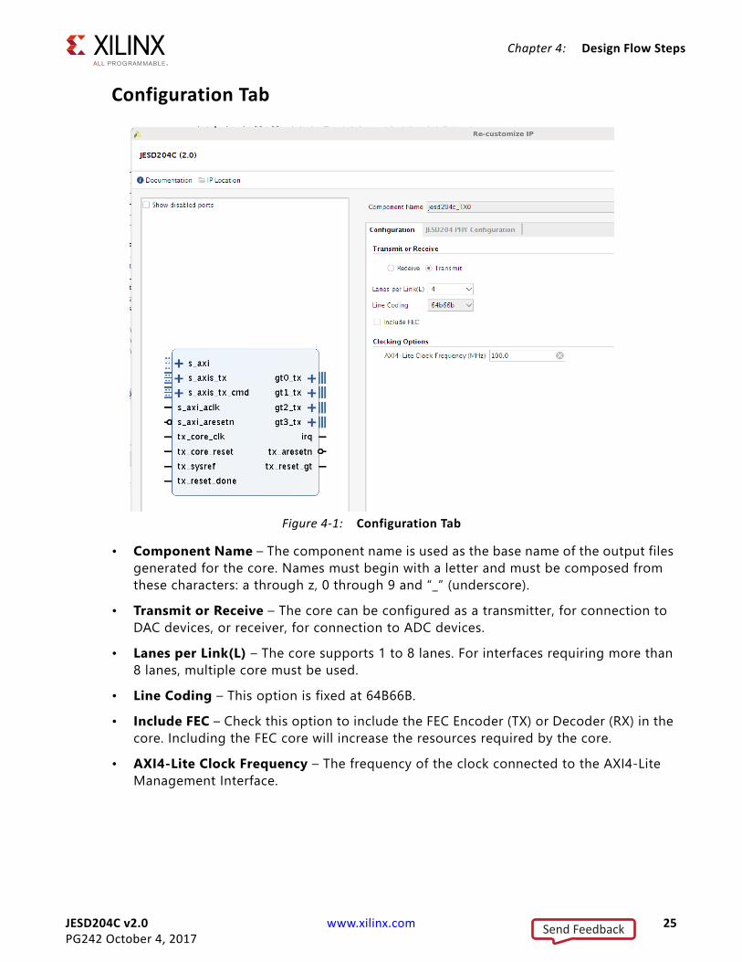
Configuration Tab
• Component Name – The component name is used as the base name of the output files generated for the core. Names must begin with a letter and must be composed from these characters: a through z, 0 through 9 and “_” (underscore).
• Transmit or Receive – The core can be configured as a transmitter, for connection to DAC devices, or receiver, for connection to ADC devices.
• Lanes per Link(L) – The core supports 1 to 8 lanes. For interfaces requiring more than 8 lanes, multiple core must be used.
• Line Coding – This option is fixed at 64B66B.• Include FEC – Check this option to include the FEC Encoder (TX) or Decoder (RX) in the
core. Including the FEC core will increase the resources required by the core.• AXI4-Lite Clock Frequency – The frequency of the clock connected to the AXI4-Lite
Management Interface.
X-Ref Target - Figure 4-1
Figure 4‐1: Configuration Tab
Send Feedback
JESD204C v2.0 www.xilinx.com 26PG242 October 4, 2017
Chapter 4: Design Flow Steps
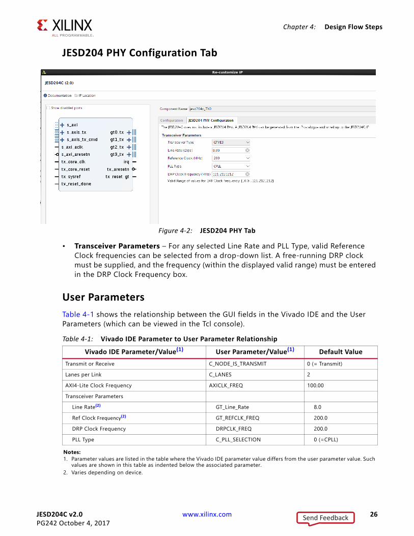
JESD204 PHY Configuration Tab
• Transceiver Parameters – For any selected Line Rate and PLL Type, valid Reference Clock frequencies can be selected from a drop-down list. A free-running DRP clock must be supplied, and the frequency (within the displayed valid range) must be entered in the DRP Clock Frequency box.
User Parameters
Table 4-1 shows the relationship between the GUI fields in the Vivado IDE and the User Parameters (which can be viewed in the Tcl console).
X-Ref Target - Figure 4-2
Figure 4‐2: JESD204 PHY Tab
Table 4‐1: Vivado IDE Parameter to User Parameter Relationship
Vivado IDE Parameter/Value(1) User Parameter/Value(1) Default Value
Transmit or Receive C_NODE_IS_TRANSMIT 0 (= Transmit)
Lanes per Link C_LANES 2
AXI4-Lite Clock Frequency AXICLK_FREQ 100.00
Transceiver Parameters
Line Rate(2) GT_Line_Rate 8.0
Ref Clock Frequency(2) GT_REFCLK_FREQ 200.0
DRP Clock Frequency DRPCLK_FREQ 200.0
PLL Type C_PLL_SELECTION 0 (=CPLL)
Notes: 1. Parameter values are listed in the table where the Vivado IDE parameter value differs from the user parameter value. Such
values are shown in this table as indented below the associated parameter.2. Varies depending on device.
Send Feedback
JESD204C v2.0 www.xilinx.com 27PG242 October 4, 2017
Chapter 4: Design Flow Steps
Output Generation
For details, see the Vivado Design Suite User Guide: Designing with IP (UG896) [Ref 2].
Transceiver Sharing
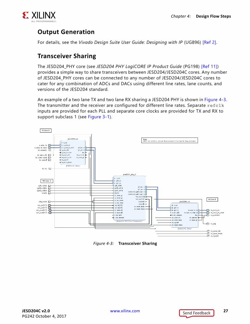
The JESD204_PHY core (see JESD204 PHY LogiCORE IP Product Guide (PG198) [Ref 11]) provides a simple way to share transceivers between JESD204/JESD204C cores. Any number of JESD204_PHY cores can be connected to any number of JESD204/JESD204C cores to cater for any combination of ADCs and DACs using different line rates, lane counts, and versions of the JESD204 standard.
An example of a two lane TX and two lane RX sharing a JESD204 PHY is shown in Figure 4-3. The transmitter and the receiver are configured for different line rates. Separate refclk inputs are provided for each PLL and separate core clocks are provided for TX and RX to support subclass 1 (see Figure 3-1).
X-Ref Target - Figure 4-3
Figure 4‐3: Transceiver Sharing
Send Feedback
JESD204C v2.0 www.xilinx.com 28PG242 October 4, 2017
Chapter 4: Design Flow Steps
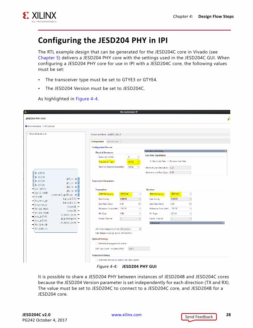
Configuring the JESD204 PHY in IPIThe RTL example design that can be generated for the JESD204C core in Vivado (see Chapter 5) delivers a JESD204 PHY core with the settings used in the JESD204C GUI. When configuring a JESD204 PHY core for use in IPI with a JESD204C core, the following values must be set:
• The transceiver type must be set to GTYE3 or GTYE4.• The JESD204 Version must be set to JESD204C.
As highlighted in Figure 4-4.
It is possible to share a JESD204 PHY between instances of JESD204B and JESD204C cores because the JESD204 Version parameter is set independently for each direction (TX and RX). The value must be set to JESD204C to connect to a JESD204C core, and JESD204B for a JESD204 core.
X-Ref Target - Figure 4-4
Figure 4‐4: JESD204 PHY GUI
Send Feedback
JESD204C v2.0 www.xilinx.com 29PG242 October 4, 2017
Chapter 4: Design Flow Steps
Constraining the CoreThis section describes how to constrain a design containing the JESD204C core. This is accomplished by using the XDC delivered with the core at generation time. An additional XDC file is generated with the IP example design; only the core XDC file should be used in user designs.
Required Constraints
This section defines the constraint requirements for the core. Constraints are provided in several XDC files which are delivered with the core and the example design to give a starting point for constraints for the user design.
There are four XDC constraint files associated with this core:
• <corename>_example_design.xdc
• <corename>_ooc.xdc
• <corename>.xdc
• <corename>_clocks.xdc
The first is used only by the example design; the second file is used for Out Of Context support where this core can be synthesized without any wrappers; the third file is the main XDC file for this core. The last file defines constraints which depend on clock period definition, either those defined by other XDC files or those generated automatically by the Xilinx tools, and this XDC file is marked for automatic late processing within the Vivado design tools to ensure that definitions exist.
Device, Package, and Speed Grade Selections
See the appropriate device data sheet listed in References to determine the maximum line rate supported. Not all devices, packages and speed grades can operate at the maximum line rate supported by the IP.
Clock Frequencies
The reference clock and core clock frequency constraints vary depending on the selected line rate and reference clock when generating the core. See the generated XDC for details.
SYSREF Constraints
The example design provided with the JESD204C core has an example of a setup and hold window assuming the SYSREF and clock have aligned edges. The following example is for a transmit design with a 1 ns setup and hold window (the exact requirements for these
Send Feedback
JESD204C v2.0 www.xilinx.com 30PG242 October 4, 2017
Chapter 4: Design Flow Steps
constraints depend on the chosen method of generating SYSREF and the board layout, the constraints provided with the core are for example only):
set_input_delay -clock clk -max 0.5 [get_ports tx_sysref]
set_input_delay -clock clk -min -0.5 [get_ports tx_sysref]
If the SYSREF input sampling edge is changed, these constraints require modification.
Clock Domains
There are also several paths where clock domains are crossed. These include the management interface. See the generated XDC file for details.
Clock Management
Reference clock and core clock resources require location constraints appropriate to your top-level design.
Clock Placement
Reference clock input should be given location constraints appropriate to your top-level design and to the placement of the transceivers.
Core clock input (if required) should be given location constraints appropriate to your top-level design.
Banking
All ports should be given location constraints appropriate to your top-level design within banking limits.
Transceiver Placement
Transceivers should be given location constraints appropriate to your design.
I/O Standard and Placement
All ports should be given I/O standard and location constraints appropriate to your top-level design.
Send Feedback
JESD204C v2.0 www.xilinx.com 31PG242 October 4, 2017
Chapter 4: Design Flow Steps
SimulationFor comprehensive information about Vivado simulation components, as well as information about using supported third party tools, see the Vivado Design Suite User Guide: Logic Simulation (UG900) [Ref 4].
IMPORTANT: For cores targeting 7 series or Zynq-7000 AP SoC devices, UNIFAST libraries are not supported. Xilinx IP is tested and qualified with UNISIM libraries only.
Synthesis and ImplementationFor details about synthesis and implementation, see the Vivado Design Suite User Guide: Designing with IP (UG896) [Ref 2].
Send Feedback
JESD204C v2.0 www.xilinx.com 32PG242 October 4, 2017
Chapter 5
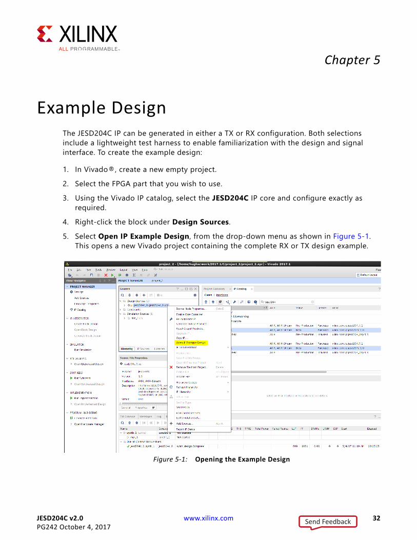
Example DesignThe JESD204C IP can be generated in either a TX or RX configuration. Both selections include a lightweight test harness to enable familiarization with the design and signal interface. To create the example design:
1. In Vivado®, create a new empty project.2. Select the FPGA part that you wish to use.3. Using the Vivado IP catalog, select the JESD204C IP core and configure exactly as
required. 4. Right-click the block under Design Sources.5. Select Open IP Example Design, from the drop-down menu as shown in Figure 5-1.
This opens a new Vivado project containing the complete RX or TX design example.X-Ref Target - Figure 5-1
Figure 5‐1: Opening the Example Design
Send Feedback
JESD204C v2.0 www.xilinx.com 33PG242 October 4, 2017
Chapter 5: Example Design
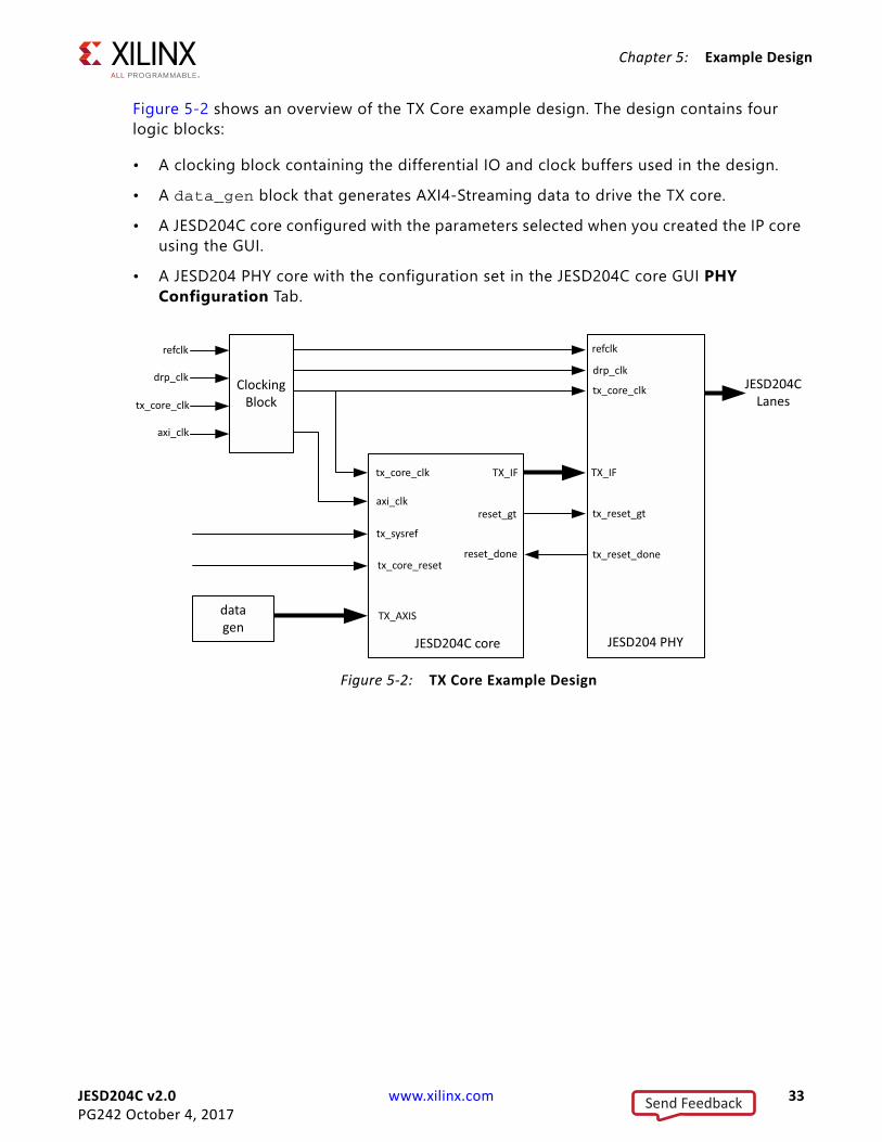
Figure 5-2 shows an overview of the TX Core example design. The design contains four logic blocks:
• A clocking block containing the differential IO and clock buffers used in the design.• A data_gen block that generates AXI4-Streaming data to drive the TX core.• A JESD204C core configured with the parameters selected when you created the IP core
using the GUI.• A JESD204 PHY core with the configuration set in the JESD204C core GUI PHY
Configuration Tab.X-Ref Target - Figure 5-2
Figure 5‐2: TX Core Example Design
ClockingBlock
refclk
tx_core_clk
axi_clk
drp_clk
tx_core_clk
axi_clk
refclk
drp_clk
tx_core_clk
TX_AXIS
tx_core_reset
datagen
tx_sysref
reset_gt
reset_done
tx_reset_gt
tx_reset_done
TX_IF TX_IF
JESD204CLanes
JESD204C core JESD204 PHY
Send Feedback
JESD204C v2.0 www.xilinx.com 34PG242 October 4, 2017
Chapter 5: Example Design
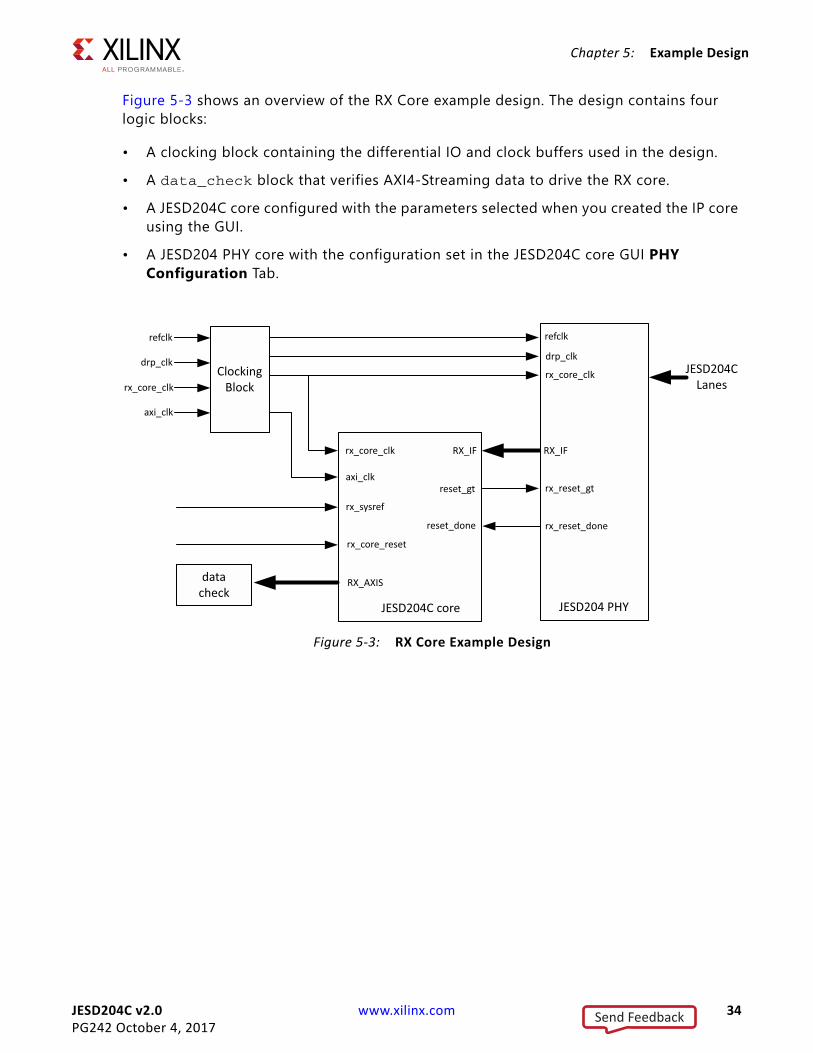
Figure 5-3 shows an overview of the RX Core example design. The design contains four logic blocks:
• A clocking block containing the differential IO and clock buffers used in the design.• A data_check block that verifies AXI4-Streaming data to drive the RX core.• A JESD204C core configured with the parameters selected when you created the IP core
using the GUI.• A JESD204 PHY core with the configuration set in the JESD204C core GUI PHY
Configuration Tab.X-Ref Target - Figure 5-3
Figure 5‐3: RX Core Example Design
ClockingBlock
refclk
rx_core_clk
axi_clk
drp_clk
rx_core_clk
axi_clk
refclk
drp_clk
rx_core_clk
RX_AXIS
rx_core_reset
datacheck
rx_sysref
reset_gt
reset_done
rx_reset_gt
rx_reset_done
RX_IF RX_IF
JESD204CLanes
JESD204C core JESD204 PHY
Send Feedback
JESD204C v2.0 www.xilinx.com 35PG242 October 4, 2017
Chapter 6
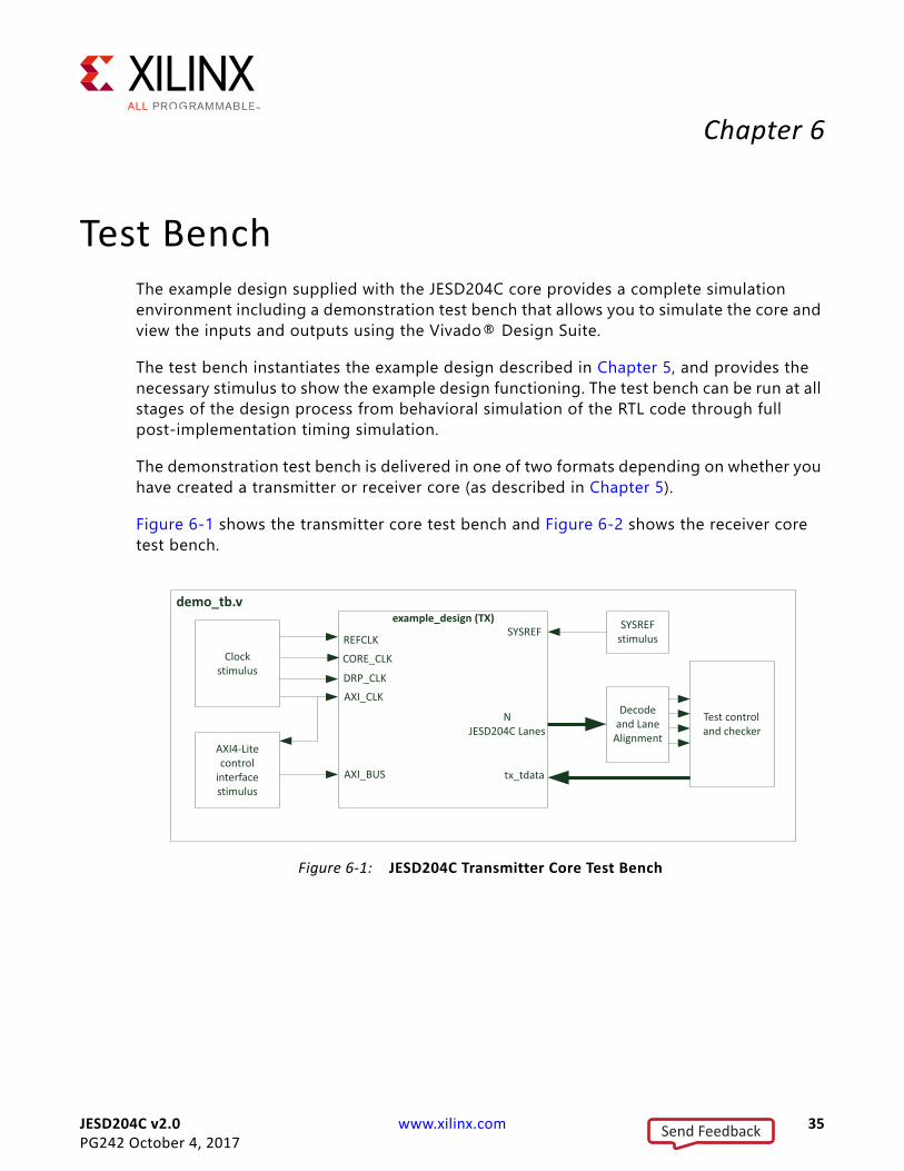
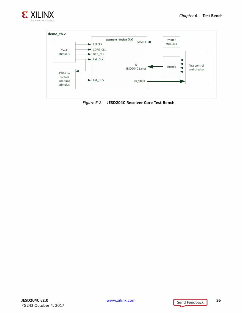
Test BenchThe example design supplied with the JESD204C core provides a complete simulation environment including a demonstration test bench that allows you to simulate the core and view the inputs and outputs using the Vivado® Design Suite.
The test bench instantiates the example design described in Chapter 5, and provides the necessary stimulus to show the example design functioning. The test bench can be run at all stages of the design process from behavioral simulation of the RTL code through full post-implementation timing simulation.
The demonstration test bench is delivered in one of two formats depending on whether you have created a transmitter or receiver core (as described in Chapter 5).
Figure 6-1 shows the transmitter core test bench and Figure 6-2 shows the receiver core test bench.X-Ref Target - Figure 6-1
Figure 6‐1: JESD204C Transmitter Core Test Bench
demo_tb.vexample_design (TX)
AXI4-Litecontrol
interfacestimulus
Clockstimulus
AXI_BUS
NJESD204C Lanes
Decodeand Lane
Alignment
tx_tdata
REFCLK
DRP_CLK
SYSREF
AXI_CLK
SYSREFstimulus
CORE_CLK
Test control and checker
Send Feedback
JESD204C v2.0 www.xilinx.com 36PG242 October 4, 2017
Chapter 6: Test Bench
X-Ref Target - Figure 6-2
Figure 6‐2: JESD204C Receiver Core Test Bench
demo_tb.vexample_design (RX)
AXI4-Lite control
interfacestimulus
Clockstimulus
REFCLK
CORE_CLK
AXI_CLK
SYSREF
AXI_BUS
Encode Test control and checker
NJESD204C Lanes
SYSREFstimulus
DRP_CLK
rx_tdata
Send Feedback
JESD204C v2.0 www.xilinx.com 37PG242 October 4, 2017
Appendix A
Verification, Compliance, and Interoperability
This appendix is not applicable until the JESD204C Standard has been ratified [Ref 9].
Send Feedback
JESD204C v2.0 www.xilinx.com 38PG242 October 4, 2017
Appendix B
Upgrading
Upgrading from v1.0 to v2.0
New ports have been added to the JESD204 PHY interface for TX and RX as follows:
• gtN_txcharisk[3:0]• gtN_rxcharisk[3:0]• gtN_rxdisperr[3:0]• gtN_rxnotintable[3:0]
These ports must be wired to the corresponding ports on the JESD204 PHY core.
Send Feedback
JESD204C v2.0 www.xilinx.com 39PG242 October 4, 2017
Appendix C
DebuggingThis appendix includes details about resources available on the Xilinx Support website and debugging tools.
TIP: If the IP generation halts with an error, there might be a license issue. See License Checkers in Chapter 1 for more details.
Finding Help on Xilinx.comTo help in the design and debug process when using the JESD204C, the Xilinx Support web page contains key resources such as product documentation, release notes, answer records, information about known issues, and links for obtaining further product support.
Documentation
This product guide is the main document associated with the JESD204C. This guide, along with documentation related to all products that aid in the design process, can be found on the Xilinx Support web page or by using the Xilinx Documentation Navigator.
Download the Xilinx Documentation Navigator from the Downloads page. For more information about this tool and the features available, open the online help after installation.
Answer Records
Answer Records include information about commonly encountered problems, helpful information on how to resolve these problems, and any known issues with a Xilinx product. Answer Records are created and maintained daily ensuring that users have access to the most accurate information available.
Answer Records for this core can be located by using the Search Support box on the main Xilinx support web page. To maximize your search results, use proper keywords such as:
• Product name• Tool message(s)
Send Feedback
JESD204C v2.0 www.xilinx.com 40PG242 October 4, 2017
Appendix C: Debugging
• Summary of the issue encountered
A filter search is available after results are returned to further target the results.
Master Answer Record for the JESD204C Core: AR: 68804
Technical Support
Xilinx provides technical support at the Xilinx Support web page for this LogiCORE™ IP product when used as described in the product documentation. Xilinx cannot guarantee timing, functionality, or support if you do any of the following:
• Implement the solution in devices that are not defined in the documentation.• Customize the solution beyond that allowed in the product documentation.• Change any section of the design labeled DO NOT MODIFY.
To contact Xilinx Technical Support, navigate to the Xilinx Support web page.
Debug ToolsThere are many tools available to address JESD204C design issues. It is important to know which tools are useful for debugging various situations.
Vivado Design Suite Debug Feature
The Vivado® Design Suite debug feature inserts logic analyzer and virtual I/O cores directly into your design. The debug feature also allow you to set trigger conditions to capture application and integrated block port signals in hardware. Captured signals can then be analyzed. This feature in the Vivado IDE is used for logic debugging and validation of a design running in Xilinx devices.
The Vivado logic analyzer is used with the logic debug LogiCORE IP cores, including:
• ILA 2.0 (and later versions)• VIO 2.0 (and later versions)
See the Vivado Design Suite User Guide: Programming and Debugging (UG908) [Ref 6].
Reference Boards
The Xilinx VCU118 evaluation board boards support the JESD204C. This board can be used to prototype designs and establish that the core can communicate with the system.
Send Feedback
JESD204C v2.0 www.xilinx.com 41PG242 October 4, 2017
Appendix C: Debugging
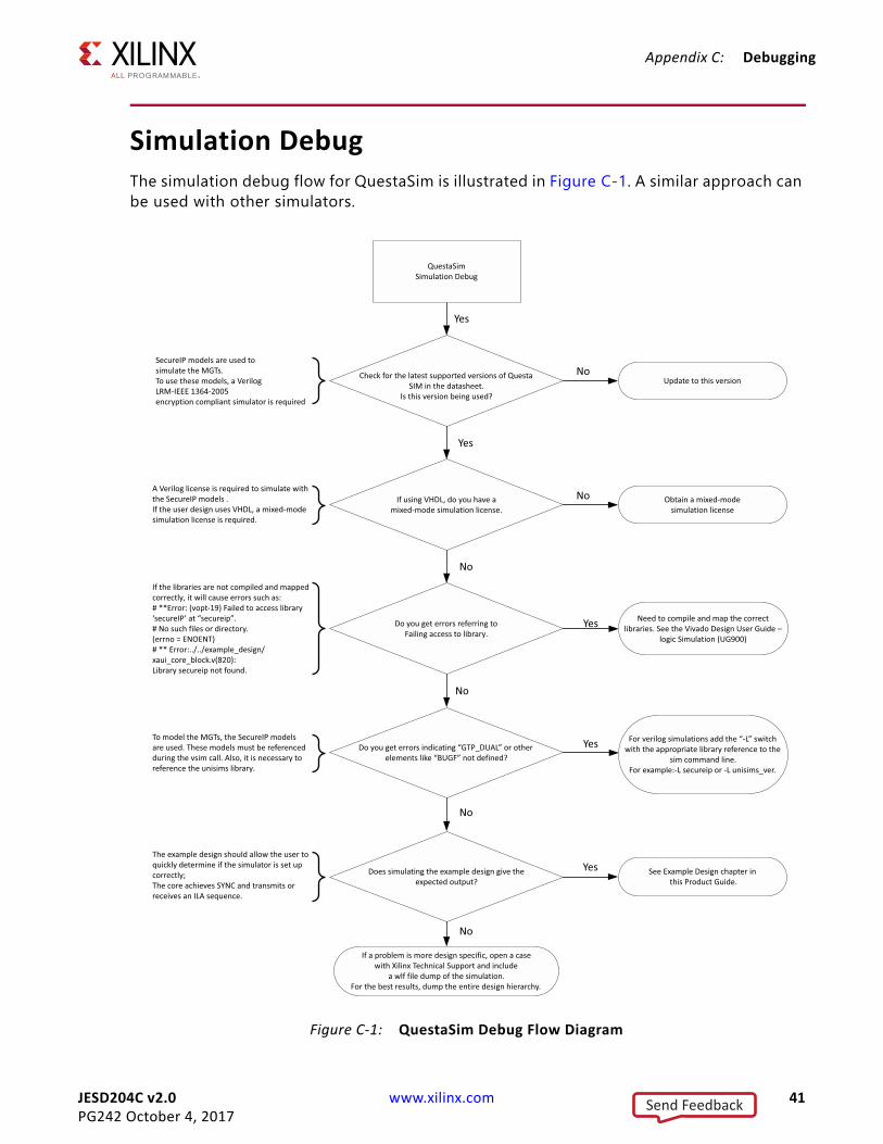
Simulation DebugThe simulation debug flow for QuestaSim is illustrated in Figure C-1. A similar approach can be used with other simulators.X-Ref Target - Figure C-1
Figure C‐1: QuestaSim Debug Flow Diagram
If a problem is more design specific, open a case with Xilinx Technical Support and include
a wlf file dump of the simulation.For the best results, dump the entire design hierarchy.
Check for the latest supported versions of Questa SIM in the datasheet.
Is this version being used?
QuestaSimSimulation Debug
If using VHDL, do you have a mixed-mode simulation license.
Do you get errors referring to Failing access to library.
Do you get errors indicating “GTP_DUAL” or other elements like “BUGF” not defined?
Does simulating the example design give the expected output?
Yes
Yes
No
No
No
No
No
Yes
Yes
Yes
Update to this version
Obtain a mixed-mode simulation license
Need to compile and map the correct libraries. See the Vivado Design User Guide –
logic Simulation (UG900)
For verilog simulations add the “-L” switch with the appropriate library reference to the
sim command line.For example:-L secureip or -L unisims_ver.
See Example Design chapter in this Product Guide.
SecureIP models are used to simulate the MGTs.To use these models, a Verilog LRM-IEEE 1364-2005 encryption compliant simulator is required
A Verilog license is required to simulate with the SecureIP models .If the user design uses VHDL, a mixed-mode simulation license is required.
If the libraries are not compiled and mapped correctly, it will cause errors such as:# **Error: (vopt-19) Failed to access library ‘secureIP’ at “secureip”.# No such files or directory.(errno = ENOENT)# ** Error:../../example_design/ xaui_core_block.v(820):Library secureip not found.
To model the MGTs, the SecureIP models are used. These models must be referenced during the vsim call. Also, it is necessary to reference the unisims library.
The example design should allow the user to quickly determine if the simulator is set up correctly;The core achieves SYNC and transmits or receives an ILA sequence.
No
Send Feedback
JESD204C v2.0 www.xilinx.com 42PG242 October 4, 2017
Appendix C: Debugging
Hardware DebugHardware issues can range from link bring-up to problems seen after hours of testing. This section provides debug steps for common issues. The debug feature is a valuable resource to use in hardware debug. The signal names mentioned in the following individual sections can be probed using the debug feature for debugging the specific problems.
General Checks
• Ensure that the core is correctly wired up and that the lane based signals are wired to the correct location on the JESD204_PHY.
• Ensure that all the timing constraints for the core were met during implementation.• Ensure that all clock sources are clean and in particular that the transceiver reference
clocks meet the transceiver requirements from the appropriate FPGA Data Sheet.• Ensure all clock sources are stable before deasserting the external reset signal to the
core.• Ensure that all transceiver PLLs have obtained lock by monitoring the QPLLLOCK_OUT
and/or CPLLLOCK_OUT port either using the debug feature or by routing the signals to a spare pin.
Issues Obtaining Lane Synchronization
• Ensure that the AXI4-Lite registers have been programmed with the correct value for multi-blocks per extended multi-block.
Interface Debug
AXI4-Lite Interfaces
Read from a register that does not have all 0s as a default to verify that the interface is functional. Output s_axi_arready asserts when the read address is valid, and output s_axi_rvalid asserts when the read data/response is valid. If the interface is unresponsive, ensure that the following conditions are met:
• The S_AXI_ACLK and ACLK inputs are connected and toggling.• The interface is not being held in reset, and S_AXI_ARESET is an active-Low reset.• The interface is enabled, and s_axi_aclken is active-High (if used).• The main core clocks are toggling and that the enables are also asserted.
Send Feedback
JESD204C v2.0 www.xilinx.com 43PG242 October 4, 2017
Appendix C: Debugging
• If the simulation has been run, verify in simulation and/or the Vivado Design Suite debug feature capture that the waveform is correct for accessing the AXI4-Lite interface.
AXI4-Stream Interfaces
If data is not being transmitted or received, check the following conditions:
• If transmit tready is stuck Low following the tvalid input being asserted, the transmit core cannot send data.
• If the receive tvalid is stuck Low following the tready input being asserted, the core is not receiving data.
• Check that the core_clk signals are connected to the TX core AXI4-Stream data source or the RX core AXI4-Stream data sink.
• Check that the AXI4-Stream waveforms are being followed (see Vivado AXI Reference Guide [Ref 10]).
• Check core configuration.
Send Feedback

JESD204C v2.0 www.xilinx.com 44PG242 October 4, 2017
Appendix D
Additional Resources and Legal Notices
Xilinx ResourcesFor support resources such as Answers, Documentation, Downloads, and Forums, see the Xilinx Support web page.
Documentation Navigator and Design HubsXilinx® Documentation Navigator provides access to Xilinx documents, videos, and support resources, which you can filter and search to find information. To open the Xilinx Documentation Navigator (DocNav):
• From the Vivado® IDE, select Help > Documentation and Tutorials.• On Windows, select Start > All Programs > Xilinx Design Tools > DocNav.• At the Linux command prompt, enter docnav.
Xilinx Design Hubs provide links to documentation organized by design tasks and other topics, which you can use to learn key concepts and address frequently asked questions. To access the Design Hubs:
• In the Xilinx Documentation Navigator, click the Design Hubs View tab.• On the Xilinx website, see the Design Hubs page.Note: For more information on Documentation Navigator, see the Documentation Navigator page on the Xilinx website.
ReferencesThese documents provide supplemental material useful with this product guide:
1. Vivado Design Suite User Guide: Designing IP Subsystems using IP Integrator (UG994)2. Vivado Design Suite User Guide: Designing with IP (UG896)
Send Feedback
JESD204C v2.0 www.xilinx.com 45PG242 October 4, 2017
Appendix D: Additional Resources and Legal Notices
3. Vivado Design Suite User Guide: Getting Started (UG910)4. Vivado Design Suite User Guide: Logic Simulation (UG900)5. ISE to Vivado Design Suite Migration Guide (UG911)6. Vivado Design Suite User Guide: Programming and Debugging (UG908)7. Vivado Design Suite User Guide: Implementation (UG904)8. AXI Interconnect LogiCORE IP Product Guide (PG059)9. JESD204C Draft www.jedec.org10. Vivado AXI Reference Guide (UG1037)11. JESD204 PHY LogiCORE IP Product Guide (PG198)
Revision HistoryThe following table shows the revision history for this document.
Date Version Revision
10/4/2017 2.0• Added ports: gtN_txcharisk[3:0], gtN_rxcharisk[3:0], gtN_rxdisperr[3:0],
gtN_rxnotintable[3:0]• Removed reference to individual parts of JESD204C specification.
06/07/2017 1.0 Added GT_POWERGOOD from JESD204_PHY to clocking example description and figure 3-2.
04/05/2017 1.0 Initial Xilinx Release.
Send Feedback

JESD204C v2.0 www.xilinx.com 46PG242 October 4, 2017
Appendix D: Additional Resources and Legal Notices
Please Read: Important Legal NoticesThe information disclosed to you hereunder (the “Materials”) is provided solely for the selection and use of Xilinx products. To the maximum extent permitted by applicable law: (1) Materials are made available “AS IS” and with all faults, Xilinx hereby DISCLAIMS ALL WARRANTIES AND CONDITIONS, EXPRESS, IMPLIED, OR STATUTORY, INCLUDING BUT NOT LIMITED TO WARRANTIES OF MERCHANTABILITY, NON-INFRINGEMENT, OR FITNESS FOR ANY PARTICULAR PURPOSE; and (2) Xilinx shall not be liable (whether in contract or tort, including negligence, or under any other theory of liability) for any loss or damage of any kind or nature related to, arising under, or in connection with, the Materials (including your use of the Materials), including for any direct, indirect, special, incidental, or consequential loss or damage (including loss of data, profits, goodwill, or any type of loss or damage suffered as a result of any action brought by a third party) even if such damage or loss was reasonably foreseeable or Xilinx had been advised of the possibility of the same. Xilinx assumes no obligation to correct any errors contained in the Materials or to notify you of updates to the Materials or to product specifications. You may not reproduce, modify, distribute, or publicly display the Materials without prior written consent. Certain products are subject to the terms and conditions of Xilinx's limited warranty, please refer to Xilinx's Terms of Sale which can be viewed at https://www.xilinx.com/legal.htm#tos; IP cores may be subject to warranty and support terms contained in a license issued to you by Xilinx. Xilinx products are not designed or intended to be fail-safe or for use in any application requiring fail-safe performance; you assume sole risk and liability for use of Xilinx products in such critical applications, please refer to Xilinx's Terms of Sale which can be viewed at https://www.xilinx.com/legal.htm#tos.AUTOMOTIVE APPLICATIONS DISCLAIMERAUTOMOTIVE PRODUCTS (IDENTIFIED AS “XA” IN THE PART NUMBER) ARE NOT WARRANTED FOR USE IN THE DEPLOYMENT OF AIRBAGS OR FOR USE IN APPLICATIONS THAT AFFECT CONTROL OF A VEHICLE (“SAFETY APPLICATION”) UNLESS THERE IS A SAFETY CONCEPT OR REDUNDANCY FEATURE CONSISTENT WITH THE ISO 26262 AUTOMOTIVE SAFETY STANDARD (“SAFETY DESIGN”). CUSTOMER SHALL, PRIOR TO USING OR DISTRIBUTING ANY SYSTEMS THAT INCORPORATE PRODUCTS, THOROUGHLY TEST SUCH SYSTEMS FOR SAFETY PURPOSES. USE OF PRODUCTS IN A SAFETY APPLICATION WITHOUT A SAFETY DESIGN IS FULLY AT THE RISK OF CUSTOMER, SUBJECT ONLY TO APPLICABLE LAWS AND REGULATIONS GOVERNING LIMITATIONS ON PRODUCT LIABILITY.© Copyright 2012–2017 Xilinx, Inc. Xilinx, the Xilinx logo, Artix, ISE, Kintex, Spartan, Virtex, Vivado, Zynq, and other designated brands included herein are trademarks of Xilinx in the United States and other countries. AMBA, AMBA Designer, ARM, ARM1176JZ-S, CoreSight, Cortex, PrimeCell, and MPCore are trademarks of ARM in the EU and other countries. All other trademarks are the property of their respective owners.
Send Feedback


![Firmware Libraries V2.0 and V2.0.x on P40C008/012/024/040 ...ST] SmartMX_P40_FWLibs2.0_2.0.x... · NXP Semicon-ductors SmartMX2 P40 FW Libraries V2.0/V2.0.x Security Target Lite Public](https://img.pdfslide.us/doc/110x75/5cfa6c1788c993613f8c995c/firmware-libraries-v20-and-v20x-on-p40c008012024040-st-smartmxp40fwlibs2020x.jpg)


![JESD204C v4.1 LogiCORE IP Product Guide · JESD204C v4.1 4 PG242 May 22, 2019 Product Specification Introduction The Xilinx® LogiCORE™ IP JESD204C core implements a JESD204C [Ref9]](https://img.pdfslide.us/doc/110x75/5f0a3b047e708231d42aa4b1/jesd204c-v41-logicore-ip-product-guide-jesd204c-v41-4-pg242-may-22-2019-product.jpg)