Embed Size (px)
Citation preview
An IMPORTANT NOTICE at the end of this TI reference design addresses authorized use, intellectual property matters and other important disclaimers and information.
TINA-TI is a trademark of Texas Instruments WEBENCH is a registered trademark of Texas Instruments
TIDU594-Oct. 2014-Revised Oct. 2014 Backup Power, Supercap, TPS61030, Data Concentrator 1 Copyright © 2014, Texas Instruments Incorporated
Jasper Li
TI Designs: PMP9755 Reference Guide
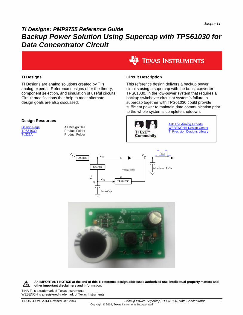
Backup Power Solution Using Supercap with TPS61030 for Data Concentrator Circuit
TI Designs Circuit Description
TI Designs are analog solutions created by TI’s analog experts. Reference designs offer the theory, component selection, and simulation of useful circuits. Circuit modifications that help to meet alternate design goals are also discussed.
This reference design delivers a backup power circuits using a supercap with the boost converter TPS61030. In the low-power system that requires a backup switchover circuit at system’s failure, a supercap together with TPS61030 could provide sufficient power to maintain data communication prior to the whole system’s complete shutdown.
Design Resources
Design Page All Design files TPS61030 Product Folder TL321A Product Folder
Ask The Analog Experts WEBENCH® Design Center TI Precision Designs Library
Charger
Vsys
SuperCap
TPS61030
Aluminum E-CapVoltage sense
Vout
I chg
Iload
Vsup
AC/DC
www.ti.com
2 Backup Power, Supercap, TPS61030, Data Concentrator TIDU594-Oct. 2014-Revised Oct. 2014 Copyright © 2014, Texas Instruments Incorporated
1 Introduction
Data concentrator is a critical device in automated metering infrastructure of smart grid. It securely aggregates the data from a number of meters and sends the data to the centralized utility servers via GPRS, GSM or other telecom networks. The data concentrator must operate for a period of time in case of the power supply failure or system brownout, which requires sufficient backup power for the equipment to the data storage or communication. So an additional energy storage device is applied in the data concentrator, either the battery or supercap. Battery has higher energy density while the supercap has better performance at output inrush current capability and lifetime which makes the supercap more competitive for the application in the data concentrator. As the output voltage of one cell supercap is not higher than 2.7V, a boost converter is needed to raise the output voltage to power the GSM/GPRS module, the voltage of which is higher than 3.6V normally. Furthermore, the low input voltage boost converter can fully utilize the supercap’s energy. This reference design illustrates a backup power solution for the data concentrator using the boost converter TPS61030 and a supercap. The design includes the schematic and layout design, components selection and performance waveforms.
www.ti.com
TIDU594-Oct. 2014-Revised Oct. 2014 Backup Power, Supercap, TPS61030, Data Concentrator 3 Copyright © 2014, Texas Instruments Incorporated
2 Design Process
2.1 Block Diagram and Operating Principle
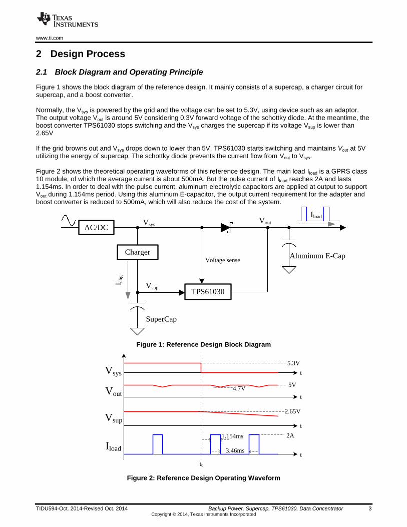
Figure 1 shows the block diagram of the reference design. It mainly consists of a supercap, a charger circuit for supercap, and a boost converter. Normally, the Vsys is powered by the grid and the voltage can be set to 5.3V, using device such as an adaptor. The output voltage Vout is around 5V considering 0.3V forward voltage of the schottky diode. At the meantime, the boost converter TPS61030 stops switching and the Vsys charges the supercap if its voltage Vsup is lower than 2.65V If the grid browns out and Vsys drops down to lower than 5V, TPS61030 starts switching and maintains Vout at 5V utilizing the energy of supercap. The schottky diode prevents the current flow from Vout to Vsys. Figure 2 shows the theoretical operating waveforms of this reference design. The main load Iload is a GPRS class 10 module, of which the average current is about 500mA. But the pulse current of Iload reaches 2A and lasts 1.154ms. In order to deal with the pulse current, aluminum electrolytic capacitors are applied at output to support Vout during 1.154ms period. Using this aluminum E-capacitor, the output current requirement for the adapter and boost converter is reduced to 500mA, which will also reduce the cost of the system.
Figure 1: Reference Design Block Diagram
Figure 2: Reference Design Operating Waveform
Charger
Vsys
SuperCap
TPS61030
Aluminum E-CapVoltage sense
Vout
I chg
Iload
Vsup
AC/DC
Iload
Vsys
5.3V
Vout
5V4.7V
2.65V
2A1.154ms
3.46ms
Vsup
t0
t
t
t
t
www.ti.com
4 Backup Power, Supercap, TPS61030, Data Concentrator TIDU594-Oct. 2014-Revised Oct. 2014 Copyright © 2014, Texas Instruments Incorporated
2.2 Schematic and Component Design
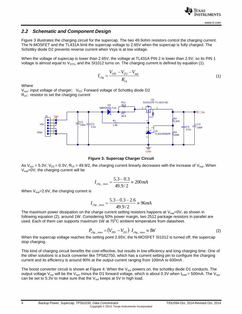
Figure 3 illustrates the charging circuit for the supercap. The two 49.9ohm resistors control the charging current. The N-MOSFET and the TL431A limit the supercap voltage to 2.65V when the supercap is fully charged. The Schottky diode D2 prevents reverse current when Vsys is at low voltage. When the voltage of supercap is lower than 2.65V, the voltage at TL431A PIN 2 is lower than 2.5V, so its PIN 1 voltage is almost equal to VSYS, and the SI1012 turns on. The charging current is defined by equation (1).
ch
DSYS
chgR
VVVI
sup2 (1)
Where Vsys: input voltage of charger; VD2: Forward voltage of Schottky diode D2 Rch: resistor to set the charging current
Figure 3: Supercap Charger Circuit
As Vsys = 5.3V, VD2 = 0.3V, Rch = 49.9/2, the charging current linearly decreases with the increase of Vsup. When Vsup=0V, the charging current will be
mAIchg 2002/9.49
3.03.5max_
When Vsup=2.6V, the charging current is
mAIchg 962/9.49
6.23.03.5max_
The maximum power dissipation on the charge current setting resistors happens at Vsup=0V, as shown in following equation (2), around 1W. Considering 50% power margin, two 2512 package resistors in parallel are used. Each of them can supports maximum 1W at 70
oC ambient temperature from datasheet.
WIVVP chgDSYSchg 1max_2max_ (2)
When the supercap voltage reaches the setting point 2.65V, the N-MOSFET SI1012 is turned off, the supercap stop charging. This kind of charging circuit benefits the cost-effective, but results in low efficiency and long charging time. One of the other solutions is a buck converter like TPS62750, which has a current setting pin to configure the charging current and its efficiency is around 90% at the output current ranging from 100mA to 600mA . The boost converter circuit is shown at Figure 4. When the Vsys powers on, the schottky diode D1 conducts. The output voltage Vout will be the Vsys minus the D1 forward voltage, which is about 0.3V when Iload = 500mA. The Vsys can be set to 5.3V to make sure that the Vout keeps at 5V in high load.
Vsys
VIN
GND100KR4
V_Sup
GND
150uC1
54
123
6
J1
100F
C3
2.2uC42.2u
C2
D2MBR0520LT1G
1.0k
R1 5.97kR2
3
21
U1TL431AIDBZR
49.9R11
49.9R3
3
1
2
Q1SI1012CR-T1-GE3-ND
www.ti.com
TIDU594-Oct. 2014-Revised Oct. 2014 Backup Power, Supercap, TPS61030, Data Concentrator 5 Copyright © 2014, Texas Instruments Incorporated
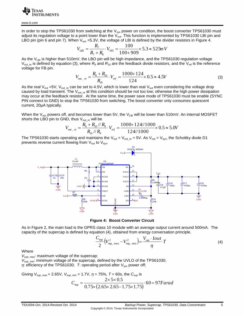
In order to stop the TPS61030 from switching at the Vsys power on condition, the boost converter TPS61030 must adjust its regulation voltage to a point lower than the Vout. This function is implemented by TPS61030 LBI pin and LBO pin (pin 6 and pin 7). When Vsys =5.3V, the voltage of LBI is defined by the divider resistors in Figure 4.
mVVRR
RV SYSLBI 5253.5
909100
100
87
7
As the VLBI is higher than 510mV, the LBO pin will be high impedance, and the TPS61030 regulation voltage Vout_re is defined by equation (3), where R6 and R10 are the feedback divide resistors, and the Vref is the reference voltage for FB pin.
VVR
RRV refreout 5.45.0
124
1241000
10
106_
(3)
As the real Vout =5V, Vout_re can be set to 4.5V, which is lower than real Vout even considering the voltage drop caused by load transient. The Vout_re at this condition should be not too low; otherwise the high power dissipation may occur at the feedback resistor. At the same time, the power save mode of TPS61030 must be enable (SYNC PIN connect to GND) to stop the TPS61030 from switching. The boost converter only consumes quiescent current, 20µA typically. When the Vsys powers off, and becomes lower than 5V, the VLBI will be lower than 510mV. An internal MOSFET shorts the LBO pin to GND, thus Vout_re will be
VVRR
RRRV refreout 0.55.0
1000//124
1000//1241000
//
//
910
9106_
The TPS61030 starts operating and maintains the Vout = Vout_re = 5V. As Vout > Vsys, the Schottky diode D1 prevents reverse current flowing from Vout to Vsys.
Figure 4: Boost Converter Circuit
As in Figure 2, the main load is the GPRS class 10 module with an average output current around 500mA. The capacity of the supercap is defined by equation (4), obtained from energy conversation principle.
TIoutV
VVC
out
2
minsup_
2
maxsup_
sup
2 (4)
Where Vsup_max: maximum voltage of the supercap; Vsup_min: minimum voltage of the supercap, defined by the UVLO of the TPS61030; η: efficiency of the TPS61030; T: operating period after Vsys power off; Giving Vsup_max = 2.65V, Vsup_min = 1.7V, η = 75%, T = 60s, the Csup is
FaradC 9760
75.175.165.265.275.0
5.052sup
SW1
SW2
PGND3
PGND4
PGND5
VBAT6
LBI7
SYNC8
EN9
LBO10
GND11
FB12
VOUT13
VOUT14
VOUT15
NC16
PG
ND
17
U2TPS61030PWP
6.1uHL1
150uC6
100kR8
GND
GND
V_Sup
Vsys
SYNC
GND
GND
GND
ENGND
GND
Vout
D1SS1P3L-M3/84A
Vsys
C510uC10
R5
909kR7
1.00MegR6
1.00Meg
R9
124kR10
1uC11
4700uC7
4700uC8
4.7µFC9
www.ti.com
6 Backup Power, Supercap, TPS61030, Data Concentrator TIDU594-Oct. 2014-Revised Oct. 2014 Copyright © 2014, Texas Instruments Incorporated
A 100Farad/2.7V supercap is selected in the reference design. The inductor peak current of TPS61030 is defined by the equation (5) from its datasheet, where L is the input inductor, and fs is the switching frequency. The TPS61030 limits its inductor peak current at typical 4A, so the maximum output current is defined by equation (6).
sout
ininout
in
outoutpeakL
fVL
VVV
V
IVI
2
1_
(5)
sout
ininoutpeakL
out
inout
fVL
VVVI
V
VI
2
1_
(6)
In the reference design, L = 6.1µH, and fs = 600kHz according to the TPS61030 datasheet. The maximum output current at Vin=1.7V is the smallest, which is
A
kI 98.0
60051.6
7.17.15
2
14
5
75.07.17.1max_
This maximum output current at Vin = 1.7V is higher than the average load current 500mA, but smaller than the peak current 2A. So an aluminum electrolytic capacitor is added at the output to support current gap during this 1.154mS period. The Vout drop can be calculated by equation (7), where Calu and ESRalu are the capacitance and effect series resistor of the aluminum electrolytic capacitor respectively.
alupeakLoad
alu
peakload
alu ESRIImsC
IIV
7.1max__
7.1max__154.1 (7)
A 4700µF capacitor EEUFR0J472 is adopted in the reference design. Its ESR is 15mΩ at 20oC. According to the
equation (7), the voltage drop of the Vout is
mVmAAmsF
AAValu 2651598.02154.1
4700
98.02
So the minimum output voltage of Vout is about 4.74V, which is high enough to support the GPRS module. Although a large aluminum electrolytic capacitor is used, A small ceramic capacitor combined with a tantalum capacitor or a ceramic capacitor larger than 47µF is still needed to absorb the switching current of the inductor, because ESL (Effective Series Inductor) of an aluminum capacitor make it not suitable to smooth high frequency voltage ripple. The small ceramic capacitor combined with a tantalum capacitor is adopted at this reference design.
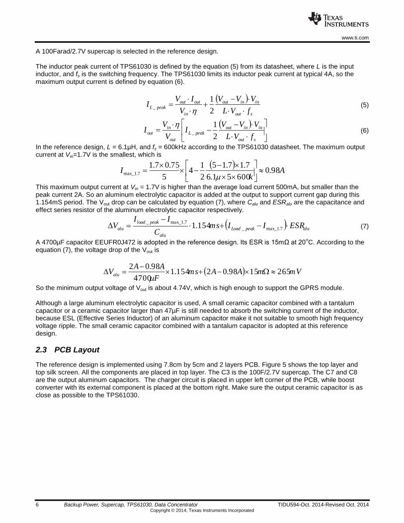
2.3 PCB Layout
The reference design is implemented using 7.8cm by 5cm and 2 layers PCB. Figure 5 shows the top layer and top silk screen. All the components are placed in top layer. The C3 is the 100F/2.7V supercap. The C7 and C8 are the output aluminum capacitors. The charger circuit is placed in upper left corner of the PCB, while boost converter with its external component is placed at the bottom right. Make sure the output ceramic capacitor is as close as possible to the TPS61030.
www.ti.com
TIDU594-Oct. 2014-Revised Oct. 2014 Backup Power, Supercap, TPS61030, Data Concentrator 7 Copyright © 2014, Texas Instruments Incorporated
Figure 5: Top Layer and Top Silkscreen
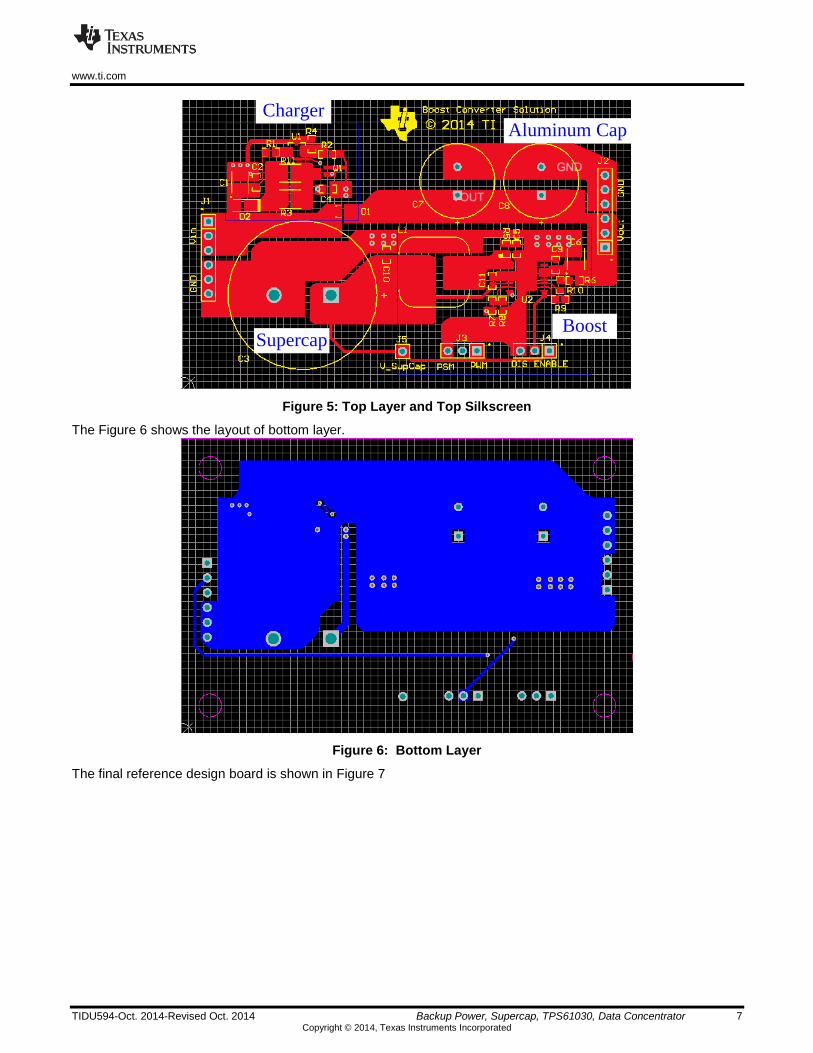
The Figure 6 shows the layout of bottom layer.
Figure 6: Bottom Layer
The final reference design board is shown in Figure 7
Supercap
Charger
Boost
Aluminum Cap
www.ti.com
8 Backup Power, Supercap, TPS61030, Data Concentrator TIDU594-Oct. 2014-Revised Oct. 2014 Copyright © 2014, Texas Instruments Incorporated
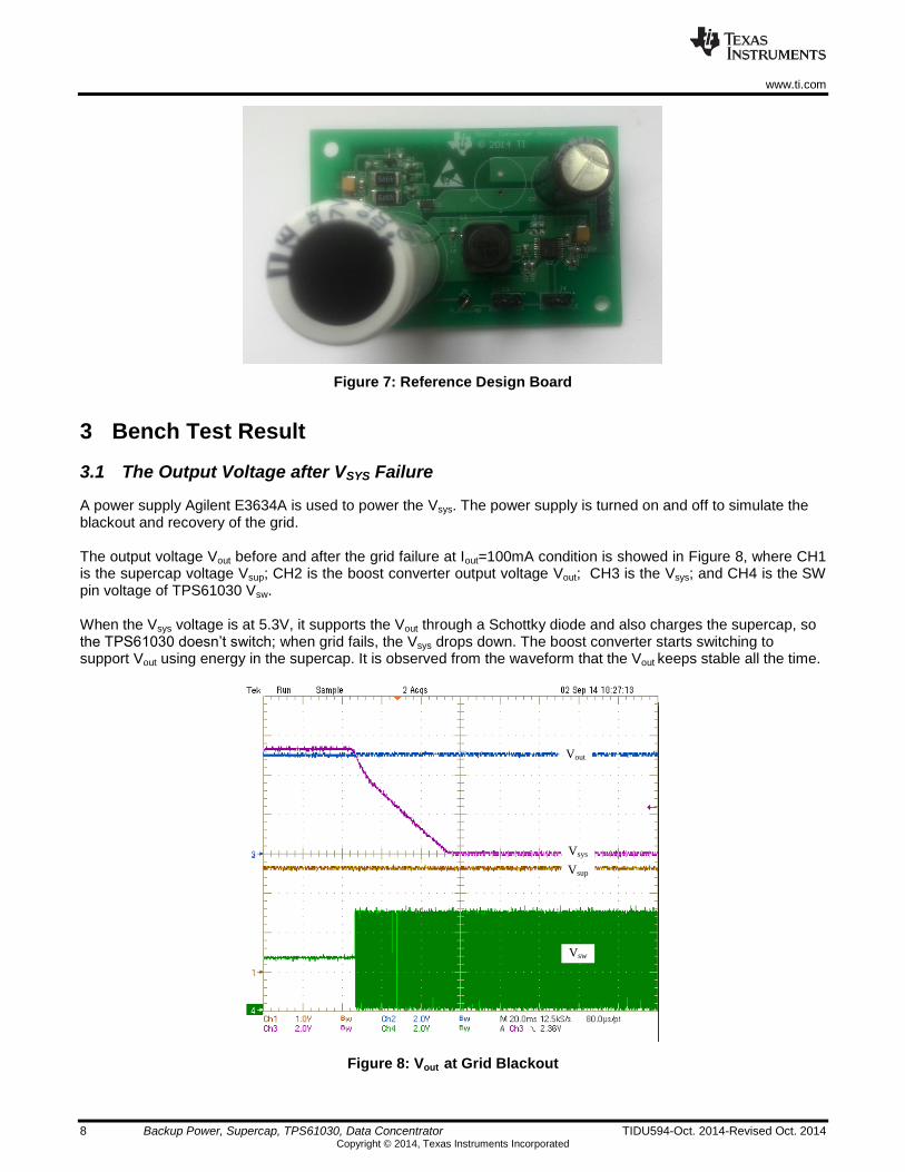
Figure 7: Reference Design Board
3 Bench Test Result
3.1 The Output Voltage after VSYS Failure
A power supply Agilent E3634A is used to power the Vsys. The power supply is turned on and off to simulate the blackout and recovery of the grid. The output voltage Vout before and after the grid failure at Iout=100mA condition is showed in Figure 8, where CH1 is the supercap voltage Vsup; CH2 is the boost converter output voltage Vout; CH3 is the Vsys; and CH4 is the SW pin voltage of TPS61030 Vsw. When the Vsys voltage is at 5.3V, it supports the Vout through a Schottky diode and also charges the supercap, so the TPS61030 doesn’t switch; when grid fails, the Vsys drops down. The boost converter starts switching to support Vout using energy in the supercap. It is observed from the waveform that the Vout keeps stable all the time.
Figure 8: Vout at Grid Blackout
Vsys
Vsup
Vsw
Vout
www.ti.com
TIDU594-Oct. 2014-Revised Oct. 2014 Backup Power, Supercap, TPS61030, Data Concentrator 9 Copyright © 2014, Texas Instruments Incorporated
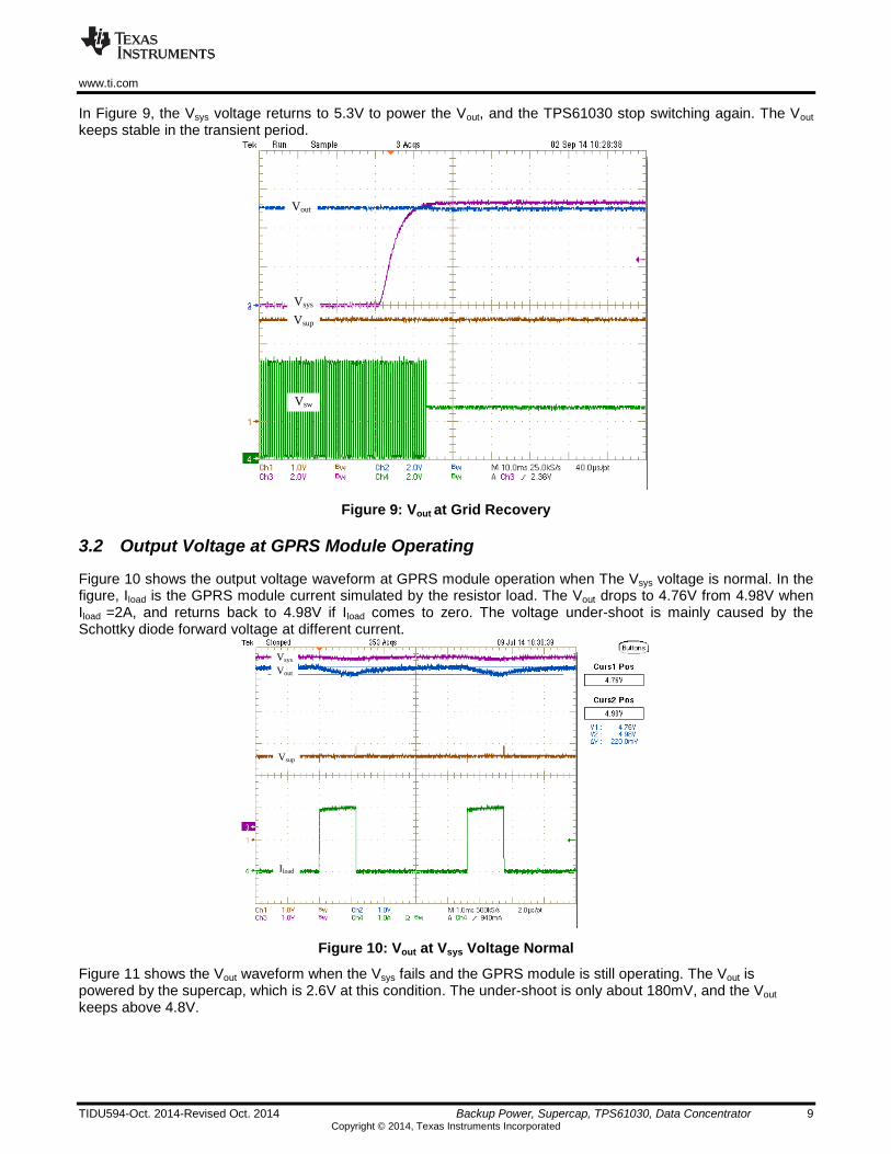
In Figure 9, the Vsys voltage returns to 5.3V to power the Vout, and the TPS61030 stop switching again. The Vout
keeps stable in the transient period.
Figure 9: Vout at Grid Recovery
3.2 Output Voltage at GPRS Module Operating
Figure 10 shows the output voltage waveform at GPRS module operation when The Vsys voltage is normal. In the figure, Iload is the GPRS module current simulated by the resistor load. The Vout drops to 4.76V from 4.98V when Iload =2A, and returns back to 4.98V if Iload comes to zero. The voltage under-shoot is mainly caused by the Schottky diode forward voltage at different current.
Figure 10: Vout at Vsys Voltage Normal
Figure 11 shows the Vout waveform when the Vsys fails and the GPRS module is still operating. The Vout is powered by the supercap, which is 2.6V at this condition. The under-shoot is only about 180mV, and the Vout keeps above 4.8V.
Vsys
Vsup
Vsw
Vout
Vsys
Vsup
Iload
Vout
www.ti.com
10 Backup Power, Supercap, TPS61030, Data Concentrator TIDU594-Oct. 2014-Revised Oct. 2014 Copyright © 2014, Texas Instruments Incorporated
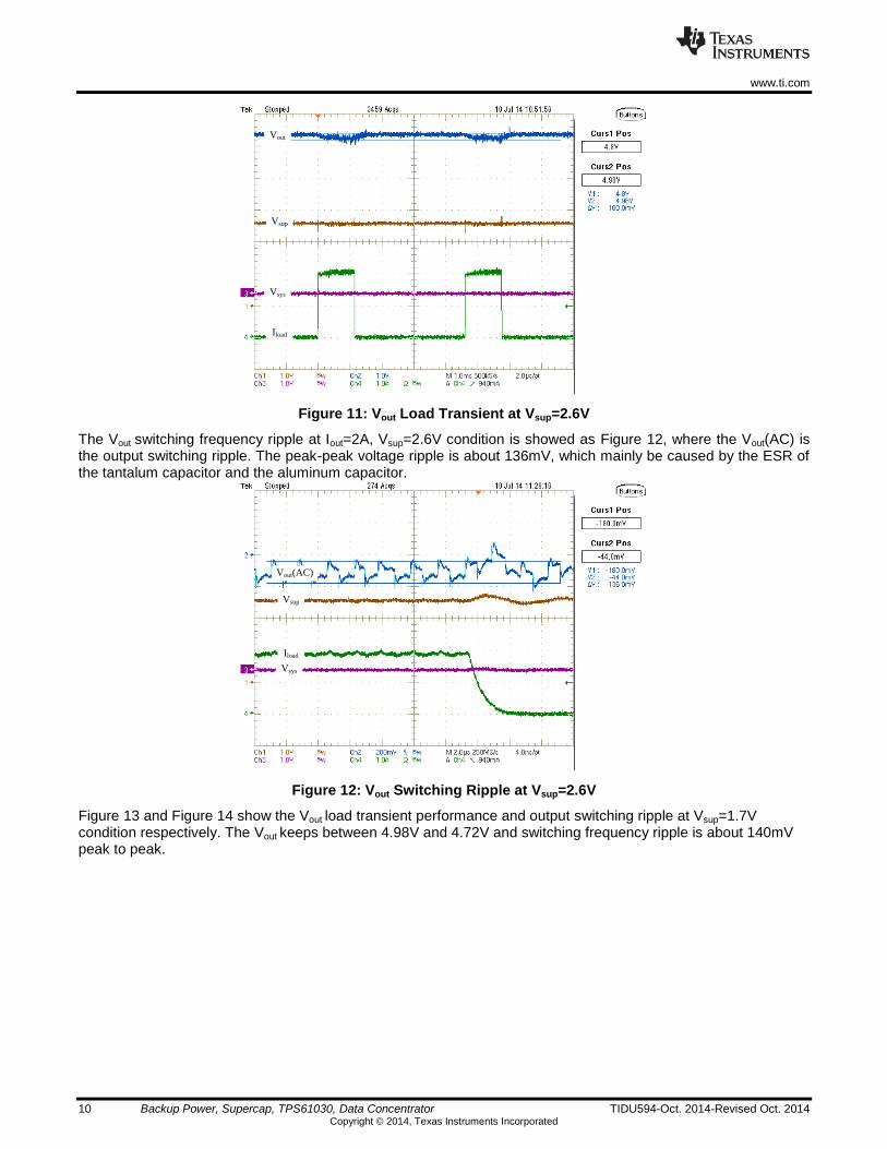
Figure 11: Vout Load Transient at Vsup=2.6V
The Vout switching frequency ripple at Iout=2A, Vsup=2.6V condition is showed as Figure 12, where the Vout(AC) is the output switching ripple. The peak-peak voltage ripple is about 136mV, which mainly be caused by the ESR of the tantalum capacitor and the aluminum capacitor.
Figure 12: Vout Switching Ripple at Vsup=2.6V
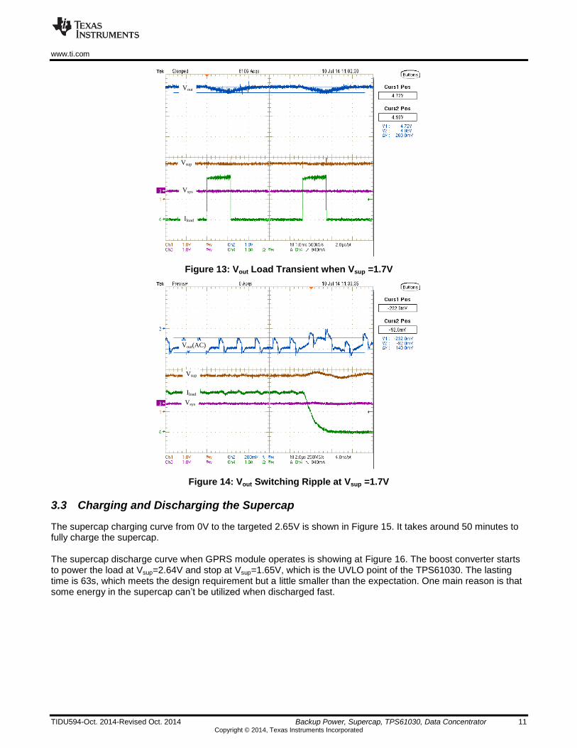
Figure 13 and Figure 14 show the Vout load transient performance and output switching ripple at Vsup=1.7V condition respectively. The Vout keeps between 4.98V and 4.72V and switching frequency ripple is about 140mV peak to peak.
Vsys
Vsup
Iload
Vout
Vsys
Vsup
Iload
Vout(AC)
www.ti.com
TIDU594-Oct. 2014-Revised Oct. 2014 Backup Power, Supercap, TPS61030, Data Concentrator 11 Copyright © 2014, Texas Instruments Incorporated
Figure 13: Vout Load Transient when Vsup =1.7V
Figure 14: Vout Switching Ripple at Vsup =1.7V
3.3 Charging and Discharging the Supercap
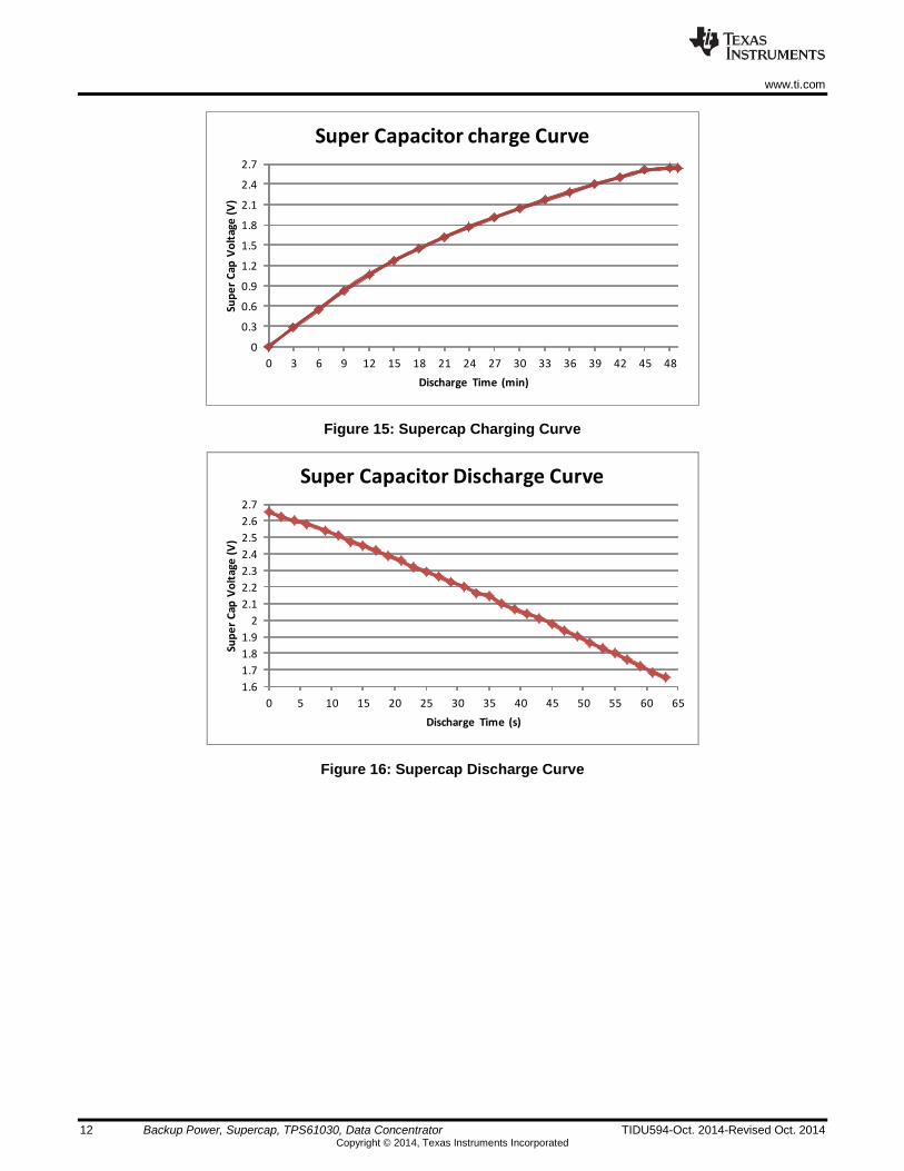
The supercap charging curve from 0V to the targeted 2.65V is shown in Figure 15. It takes around 50 minutes to fully charge the supercap. The supercap discharge curve when GPRS module operates is showing at Figure 16. The boost converter starts to power the load at Vsup=2.64V and stop at Vsup=1.65V, which is the UVLO point of the TPS61030. The lasting time is 63s, which meets the design requirement but a little smaller than the expectation. One main reason is that some energy in the supercap can’t be utilized when discharged fast.
Vsys
Vsup
Iload
Vout
Vsys
Vsup
Iload
Vout(AC)
www.ti.com
12 Backup Power, Supercap, TPS61030, Data Concentrator TIDU594-Oct. 2014-Revised Oct. 2014 Copyright © 2014, Texas Instruments Incorporated
Figure 15: Supercap Charging Curve
Figure 16: Supercap Discharge Curve
0
0.3
0.6
0.9
1.2
1.5
1.8
2.1
2.4
2.7
0 3 6 9 12 15 18 21 24 27 30 33 36 39 42 45 48
Sup
er
Cap
Vo
ltag
e (
V)
Discharge Time (min)
Super Capacitor charge Curve
1.6
1.7
1.8
1.9
2
2.1
2.2
2.3
2.4
2.5
2.6
2.7
0 5 10 15 20 25 30 35 40 45 50 55 60 65
Sup
er
Cap
Vo
ltag
e (
V)
Discharge Time (s)
Super Capacitor Discharge Curve
IMPORTANT NOTICE FOR TI REFERENCE DESIGNSTexas Instruments Incorporated ("TI") reference designs are solely intended to assist designers (“Buyers”) who are developing systems thatincorporate TI semiconductor products (also referred to herein as “components”). Buyer understands and agrees that Buyer remainsresponsible for using its independent analysis, evaluation and judgment in designing Buyer’s systems and products.TI reference designs have been created using standard laboratory conditions and engineering practices. TI has not conducted anytesting other than that specifically described in the published documentation for a particular reference design. TI may makecorrections, enhancements, improvements and other changes to its reference designs.Buyers are authorized to use TI reference designs with the TI component(s) identified in each particular reference design and to modify thereference design in the development of their end products. HOWEVER, NO OTHER LICENSE, EXPRESS OR IMPLIED, BY ESTOPPELOR OTHERWISE TO ANY OTHER TI INTELLECTUAL PROPERTY RIGHT, AND NO LICENSE TO ANY THIRD PARTY TECHNOLOGYOR INTELLECTUAL PROPERTY RIGHT, IS GRANTED HEREIN, including but not limited to any patent right, copyright, mask work right,or other intellectual property right relating to any combination, machine, or process in which TI components or services are used.Information published by TI regarding third-party products or services does not constitute a license to use such products or services, or awarranty or endorsement thereof. Use of such information may require a license from a third party under the patents or other intellectualproperty of the third party, or a license from TI under the patents or other intellectual property of TI.TI REFERENCE DESIGNS ARE PROVIDED "AS IS". TI MAKES NO WARRANTIES OR REPRESENTATIONS WITH REGARD TO THEREFERENCE DESIGNS OR USE OF THE REFERENCE DESIGNS, EXPRESS, IMPLIED OR STATUTORY, INCLUDING ACCURACY ORCOMPLETENESS. TI DISCLAIMS ANY WARRANTY OF TITLE AND ANY IMPLIED WARRANTIES OF MERCHANTABILITY, FITNESSFOR A PARTICULAR PURPOSE, QUIET ENJOYMENT, QUIET POSSESSION, AND NON-INFRINGEMENT OF ANY THIRD PARTYINTELLECTUAL PROPERTY RIGHTS WITH REGARD TO TI REFERENCE DESIGNS OR USE THEREOF. TI SHALL NOT BE LIABLEFOR AND SHALL NOT DEFEND OR INDEMNIFY BUYERS AGAINST ANY THIRD PARTY INFRINGEMENT CLAIM THAT RELATES TOOR IS BASED ON A COMBINATION OF COMPONENTS PROVIDED IN A TI REFERENCE DESIGN. IN NO EVENT SHALL TI BELIABLE FOR ANY ACTUAL, SPECIAL, INCIDENTAL, CONSEQUENTIAL OR INDIRECT DAMAGES, HOWEVER CAUSED, ON ANYTHEORY OF LIABILITY AND WHETHER OR NOT TI HAS BEEN ADVISED OF THE POSSIBILITY OF SUCH DAMAGES, ARISING INANY WAY OUT OF TI REFERENCE DESIGNS OR BUYER’S USE OF TI REFERENCE DESIGNS.TI reserves the right to make corrections, enhancements, improvements and other changes to its semiconductor products and services perJESD46, latest issue, and to discontinue any product or service per JESD48, latest issue. Buyers should obtain the latest relevantinformation before placing orders and should verify that such information is current and complete. All semiconductor products are soldsubject to TI’s terms and conditions of sale supplied at the time of order acknowledgment.TI warrants performance of its components to the specifications applicable at the time of sale, in accordance with the warranty in TI’s termsand conditions of sale of semiconductor products. Testing and other quality control techniques for TI components are used to the extent TIdeems necessary to support this warranty. Except where mandated by applicable law, testing of all parameters of each component is notnecessarily performed.TI assumes no liability for applications assistance or the design of Buyers’ products. Buyers are responsible for their products andapplications using TI components. To minimize the risks associated with Buyers’ products and applications, Buyers should provideadequate design and operating safeguards.Reproduction of significant portions of TI information in TI data books, data sheets or reference designs is permissible only if reproduction iswithout alteration and is accompanied by all associated warranties, conditions, limitations, and notices. TI is not responsible or liable forsuch altered documentation. Information of third parties may be subject to additional restrictions.Buyer acknowledges and agrees that it is solely responsible for compliance with all legal, regulatory and safety-related requirementsconcerning its products, and any use of TI components in its applications, notwithstanding any applications-related information or supportthat may be provided by TI. Buyer represents and agrees that it has all the necessary expertise to create and implement safeguards thatanticipate dangerous failures, monitor failures and their consequences, lessen the likelihood of dangerous failures and take appropriateremedial actions. Buyer will fully indemnify TI and its representatives against any damages arising out of the use of any TI components inBuyer’s safety-critical applications.In some cases, TI components may be promoted specifically to facilitate safety-related applications. With such components, TI’s goal is tohelp enable customers to design and create their own end-product solutions that meet applicable functional safety standards andrequirements. Nonetheless, such components are subject to these terms.No TI components are authorized for use in FDA Class III (or similar life-critical medical equipment) unless authorized officers of the partieshave executed an agreement specifically governing such use.Only those TI components that TI has specifically designated as military grade or “enhanced plastic” are designed and intended for use inmilitary/aerospace applications or environments. Buyer acknowledges and agrees that any military or aerospace use of TI components thathave not been so designated is solely at Buyer's risk, and Buyer is solely responsible for compliance with all legal and regulatoryrequirements in connection with such use.TI has specifically designated certain components as meeting ISO/TS16949 requirements, mainly for automotive use. In any case of use ofnon-designated products, TI will not be responsible for any failure to meet ISO/TS16949.
Mailing Address: Texas Instruments, Post Office Box 655303, Dallas, Texas 75265Copyright © 2014, Texas Instruments Incorporated