Embed Size (px)
Citation preview

Report No.: JR442807-03AE Page No. : 1 of 19
Report Version: Rev. 01
Japan Test Report
Equipment : Intelligent BT4.0 Dual Mode USB Dongle
Model No. : BT900-US
Brand Name : Laird Technologies
Applicant : Laird Technologies
Address : 11160 Thompson Ave., Lenexa, Kansas 66219, USA
Standard : ARIB STD-T66 Ver. 3.7
Received Date : Oct. 22, 2015
Tested Date : Oct. 22, 2015
Measurement was conducted by the following test method: the test method of Ordinance Concerning Technical Regulations Conformity Certification etc. of Specified Radio Equipment in Annex 1, the Ministry of Internal Affairs and Communication notification in Annex “43” of Article 88, Paragraph 1 or the test method more than equivalent. We, International Certification Corp., would like to declare that the tested sample has been evaluated and in compliance with the requirement of the above standards. The test results contained in this report refer exclusively to the product. It may be duplicated completely for legal use with the approval of the applicant. It shall not be reproduced except in full without the written approval of our laboratory. Approved & Reviewed by:
Gary Chang / Manager Ty: XXX

Report No.: JR442807-03AE Page No. : 2 of 19
Report Version: Rev. 01
Table of Contents 1 GENERAL DESCRIPTION .................................................................................................................... 5
1.1 Information .............................................................................................................................................. 5 1.2 Test Equipment and Calibration Data .................................................................................................... 7 1.3 Testing Applied Standards ..................................................................................................................... 7 1.4 Measurement Uncertainty ...................................................................................................................... 7
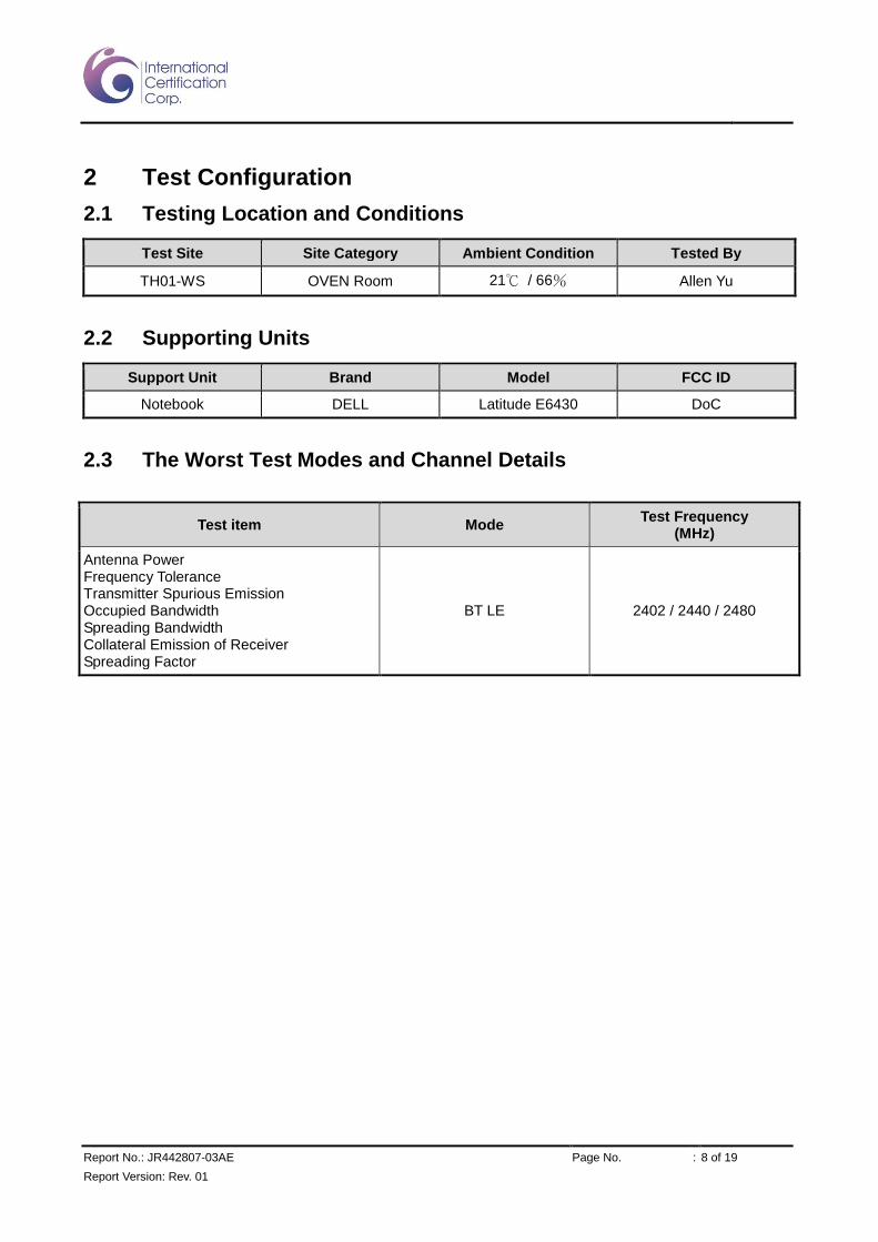
2 TEST CONFIGURATION ....................................................................................................................... 8
2.1 Testing Location and Conditions ............................................................................................................ 8 2.2 Supporting Units ..................................................................................................................................... 8 2.3 The Worst Test Modes and Channel Details ......................................................................................... 8
3 TRANSMITTER TEST RESULTS .......................................................................................................... 9
3.1 Antenna Power ....................................................................................................................................... 9 3.2 Frequency Tolerance ........................................................................................................................... 11 3.3 Occupied Bandwidth ............................................................................................................................ 12 3.4 Spreading Bandwidth and Factor ......................................................................................................... 13 3.5 Transmitter Spurious Emissions ........................................................................................................... 14 3.6 Interference prevention function ........................................................................................................... 15
4 RECEIVER TEST RESULTS ............................................................................................................... 16
4.1 Receiver Spurious Emissions ............................................................................................................... 16
5 PHOTOGRAPHS OF THE TEST CONFIGURATION ......................................................................... 17
6 TEST LABORATORY INFORMATION ............................................................................................... 19
APPENDIX A. TEST RESULTS ...................................................................................................................... A1
APPENDIX B. ANTENNA INFORMATION ..................................................................................................... B1
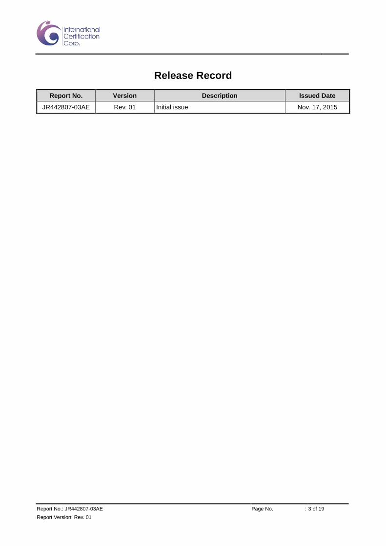
Report No.: JR442807-03AE Page No. : 3 of 19
Report Version: Rev. 01
Release Record
Report No. Version Description Issued Date
JR442807-03AE Rev. 01 Initial issue Nov. 17, 2015

Report No.: JR442807-03AE Page No. : 4 of 19
Report Version: Rev. 01
Summary of Test Results
Ref. Std. Clause Description Result
3.2(2)(3) Antenna Power Pass
3.2(4) Frequency Tolerance Pass
3.2(6) Transmitter Spurious Emission Pass
3.2(7) Occupied Bandwidth Pass
3.2(8) Spreading Bandwidth Pass
3.2(9) Spreading Factor Pass
3.3(1) Receiver Emission Pass
3.4.1 Interference prevention function Pass
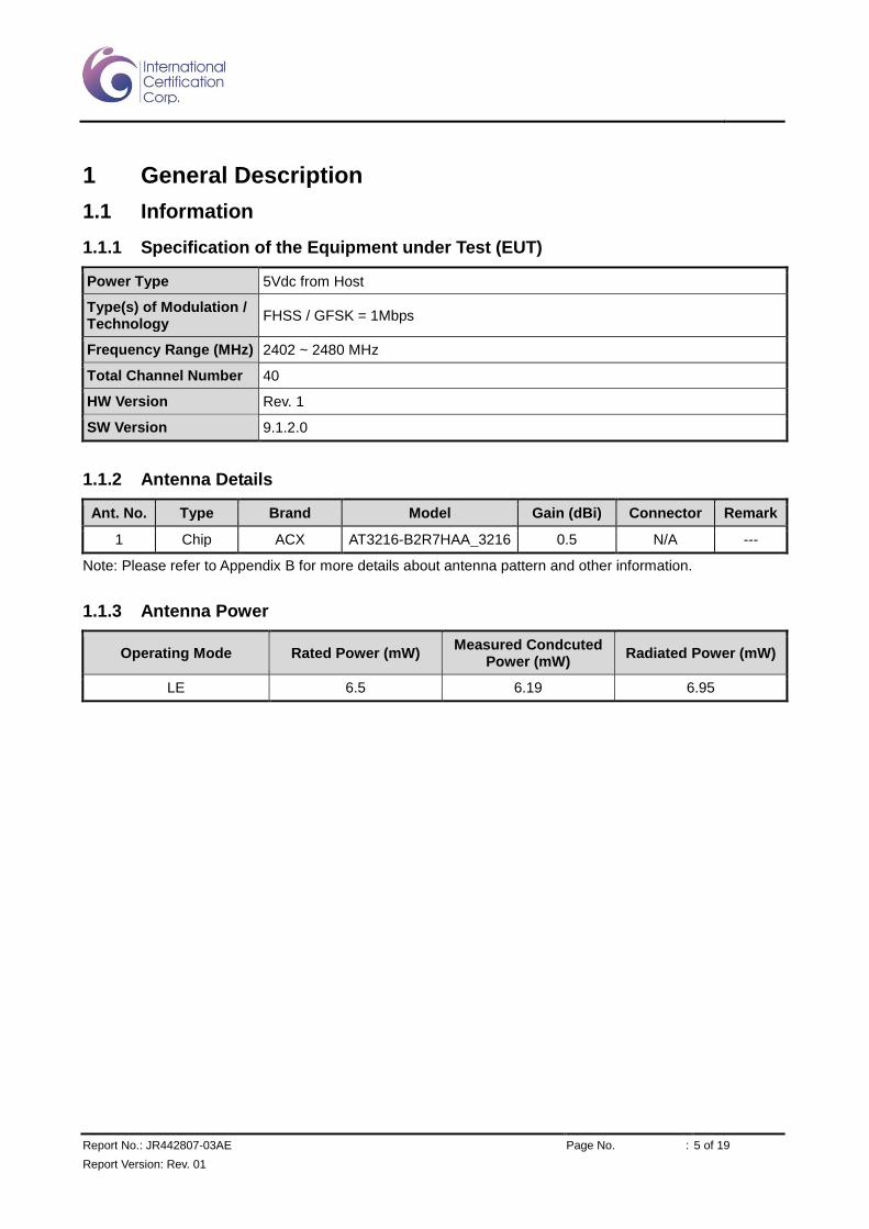
Report No.: JR442807-03AE Page No. : 5 of 19
Report Version: Rev. 01
1 General Description
1.1 Information
1.1.1 Specification of the Equipment under Test (EUT)
Power Type 5Vdc from Host
Type(s) of Modulation / Technology
FHSS / GFSK = 1Mbps
Frequency Range (MHz) 2402 ~ 2480 MHz
Total Channel Number 40
HW Version Rev. 1
SW Version 9.1.2.0
1.1.2 Antenna Details
Ant. No. Type Brand Model Gain (dBi) Connector Remark
1 Chip ACX AT3216-B2R7HAA_3216 0.5 N/A ---
Note: Please refer to Appendix B for more details about antenna pattern and other information.
1.1.3 Antenna Power
Operating Mode Rated Power (mW) Measured Condcuted
Power (mW) Radiated Power (mW)
LE 6.5 6.19 6.95

Report No.: JR442807-03AE Page No. : 6 of 19
Report Version: Rev. 01
1.1.4 Channel List
Frequency band (MHz) 2400~2483.5
Channel Frequency
(MHz) Channel
Frequency (MHz)
Channel Frequency
(MHz) Channel
Frequency (MHz)
37 2402 9 2422 18 2442 28 2462
0 2404 10 2424 19 2444 29 2464
1 2406 38 2426 20 2446 30 2466
2 2408 11 2428 21 2448 31 2468
3 2410 12 2430 22 2450 32 2470
4 2412 13 2432 23 2452 33 2472
5 2414 14 2434 24 2454 34 2474
6 2416 15 2436 25 2456 35 2476
7 2418 16 2438 26 2458 36 2478
8 2420 17 2440 27 2460 39 2480
1.1.5 Test Tool and Power Setting
Test Tool
CSR Blue Test3 v.2.5.8
Modulation Mode Test Frequency (MHz)
2402 2440 2480
GFSK/1Mbps Default Default Default
1.1.6 Protection Method for High Frequency and Modulation Section
Protected Method Description
Shielding Case RF and Modulation components are covered with shielding case and this shielding case is soldered.
Photo

Report No.: JR442807-03AE Page No. : 7 of 19
Report Version: Rev. 01
1.2 Test Equipment and Calibration Data
Test Item RF Conducted
Test Site (TH01-WS)
Instrument Manufacturer Model No. Serial No. Calibration Date Calibration Until
Spectrum Analyzer R&S FSV40 101063 Feb. 03, 2015 Feb. 02, 2016
Power Meter Anritsu ML2495A 1241002 Sep. 21, 2015 Sep. 20, 2016
Power Sensor Anritsu MA2411B 1207366 Sep. 21, 2015 Sep. 20, 2016
Signal Generator R&S SMB100A 175727 Oct. 05, 2015 Oct. 04, 2016
DC POWER SOURCE
GW INSTEK GPC-3060D EM884797 Oct. 20, 2015 Oct. 19, 2016
Measurement Software
Sporton Sporton_1 1.3.30 NA NA
Measurement Software
Agilent EN RF test 1.140904 NA NA
Note: Calibration Interval of instruments listed above is one year. Note 2: Above instruments are calibrated by Electronics Testing Center
1.3 Testing Applied Standards
According to the specifications of the manufacturer, the EUT must comply with the requirements of the following standards:
ARIB STD-T66 Ver. 3.7
1.4 Measurement Uncertainty
ISO/IEC 17025 requires that an estimate of the measurement uncertainties associated with the emissions test results be included in the report. The measurement uncertainties given below are based on a 95% confidence level (based on a coverage factor (k=2)
Measurement Uncertainty
Parameters Uncertainty
Frequency error ±33.988 Hz
Bandwidth ±33.988 Hz
Conducted power ±0.537 dB
TX Conducted emission ±2.308 dB
RX Conducted emission ±2.525 dB
Report No.: JR442807-03AE Page No. : 8 of 19
Report Version: Rev. 01
2 Test Configuration
2.1 Testing Location and Conditions
Test Site Site Category Ambient Condition Tested By
TH01-WS OVEN Room 21 / 66% Allen Yu
2.2 Supporting Units
Support Unit Brand Model FCC ID
Notebook DELL Latitude E6430 DoC
2.3 The Worst Test Modes and Channel Details
Test item Mode Test Frequency
(MHz)
Antenna Power Frequency Tolerance Transmitter Spurious Emission Occupied Bandwidth Spreading Bandwidth Collateral Emission of Receiver Spreading Factor
BT LE 2402 / 2440 / 2480
Report No.: JR442807-03AE Page No. : 9 of 19
Report Version: Rev. 01
3 Transmitter Test Results
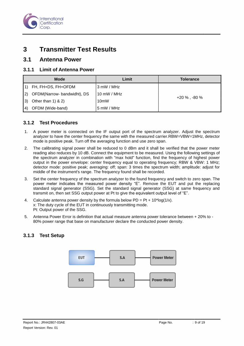
3.1 Antenna Power
3.1.1 Limit of Antenna Power
Mode Limit Tolerance
1) FH, FH+DS, FH+OFDM 3 mW / MHz
+20 % , -80 % 2) OFDM(Narrow- bandwidht), DS 10 mW / MHz
3) Other than 1) & 2) 10mW
4) OFDM (Wide-band) 5 mW / MHz
3.1.2 Test Procedures
1. A power meter is connected on the IF output port of the spectrum analyzer. Adjust the spectrum analyzer to have the center frequency the same with the measured carrier.RBW=VBW=1MHz, detector mode is positive peak. Turn off the averaging function and use zero span.
2. The calibrating signal power shall be reduced to 0 dBm and it shall be verified that the power meter reading also reduces by 10 dB. Connect the equipment to be measured. Using the following settings of the spectrum analyzer in combination with "max hold" function, find the frequency of highest power output in the power envelope: center frequency equal to operating frequency; RBW & VBW: 1 MHz; detector mode: positive peak; averaging: off; span: 3 times the spectrum width; amplitude: adjust for middle of the instrument's range. The frequency found shall be recorded.
3. Set the center frequency of the spectrum analyzer to the found frequency and switch to zero span. The power meter indicates the measured power density “E”. Remove the EUT and put the replacing standard signal generator (SSG). Set the standard signal generator (SSG) at same frequency and transmit on, then set SSG output power at Pt to give the equivalent output level of “E”.
4. Calculate antenna power density by the formula below PD = Pt + 10*log(1/x). x: The duty cycle of the EUT in continuously transmitting mode. Pt: Output power of the SSG.
5. Antenna Power Error is definition that actual measure antenna power tolerance between + 20% to - 80% power range that base on manufacturer declare the conducted power density.
3.1.3 Test Setup

Report No.: JR442807-03AE Page No. : 10 of 19
Report Version: Rev. 01
3.1.4 Test Result of Maximum Transmit Power
Reference Documents Test Mode Test Items
Appendix A 19-LE LE 1.Test Results 2. Antenna Power (Conducted Power)

Report No.: JR442807-03AE Page No. : 11 of 19
Report Version: Rev. 01
3.2 Frequency Tolerance
3.2.1 Limit of Frequency Tolerance
Frequency tolerance shall be +/- 50ppm.
3.2.2 Test Procedures
1. Set Span = 150kHz, RBW = 1kHz, VBW = 30kHz, Sweep time = Auto, detector = Peak.
2. Use Peak search function to find the max peak value and record this value (RF).
3. Calculate frequency tolerance by below formula
FT(ppm) = (RF) – (MF) / (MF) × 1000000
(FT: Frequency Tolerance, RF: Reading Frequency, MF: Measurement Frequency.)
3.2.3 Test Setup
3.2.4 Test Result of Frequency Tolerance
Reference Documents Test Mode Test Items
Appendix A 19-LE LE 1.Test Results
Report No.: JR442807-03AE Page No. : 12 of 19
Report Version: Rev. 01
3.3 Occupied Bandwidth
3.3.1 Limit of Occupied Bandwidth
Mode Limit (MHz)
FH 83.5
FH+DS 83.5
FH+OFDM 83.5
OFDM(Narrow- bandwidht), DS 26
Others 26
OFDM (Wide-band) 38
3.3.2 Test Procedures
1. Set Span = 40MHz, RBW = VBW = 300kHz, detector = Peak, Sweep time = Auto.
2. Enable OBW function of spectrum analyzer to measure OBW and capture test plot.
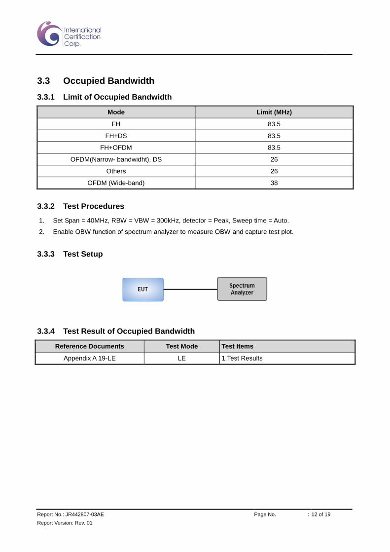
3.3.3 Test Setup
3.3.4 Test Result of Occupied Bandwidth
Reference Documents Test Mode Test Items
Appendix A 19-LE LE 1.Test Results
Report No.: JR442807-03AE Page No. : 13 of 19
Report Version: Rev. 01
3.4 Spreading Bandwidth and Factor
3.4.1 Limit of Spreading Bandwidth and Factor
Item Limit
Spreading bandwidth ≥ 500kHz
Spreading factor for DSSS (operates at 2400~2483.5 MHz) ≥ 5
Spreading factor for DSSS (operates at 2471~2497 MHz) ≥ 10
3.4.2 Test Procedures
1. Set Span = 20MHz, RBW = VBW = 300kHz, detector = Peak, Sweep time = Auto.
2. Enable OBW (90%) function of spectrum analyzer to measure OBW (90%) and capture test plot.
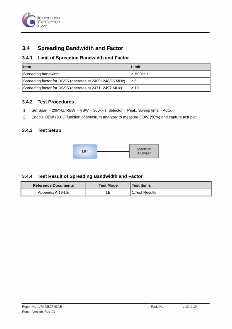
3.4.3 Test Setup
3.4.4 Test Result of Spreading Bandwidth and Factor
Reference Documents Test Mode Test Items
Appendix A 19-LE LE 1.Test Results

Report No.: JR442807-03AE Page No. : 14 of 19
Report Version: Rev. 01
3.5 Transmitter Spurious Emissions
3.5.1 Limit of Transmitter Spurious Emissions
Item Limits
Tx Spurious Emission
≤ 2.5 μW (2387MHz > f ; 2496.5MHz < f ).
≤ 25 μW. (2387MHz ≤ f < 2400MHz) and (2483.5MHz < f ≤ 2496.5MHz).
3.5.2 Test Procedures
1. Set EUT to transmit at rated power and channel to perform test.
2. Set RBW = VBW = 1MHz, Detector type = Peak, Sweep time = Auto.
3. Following above setting of spectrum analyzer to measure spurious emission of 30~12750 MHz.
3.5.3 Test Setup
3.5.4 Test Result of Transmitter Spurious Emissions
Reference Documents Test Mode Test Items
Appendix A 19-LE LE 1.Test Results 5. Unwanted Emission Intensity

Report No.: JR442807-03AE Page No. : 15 of 19
Report Version: Rev. 01
3.6 Interference prevention function
3.6.1 Limit of Interference Prevention Function
Limits
The identification code shall be 48 bits long
3.6.2 Test Procedures
1. Set EUT under operating mode and link up with companion equipment
2. Check communication status between EUT and companion equipment is normal
3. Confirm the MAC address of EUT
3.6.3 Test Setup
3.6.4 Test Result of Interference Prevention Function
Reference Documents Test Mode Test Items
Appendix A 19-LE LE 1.Test Results
Report No.: JR442807-03AE Page No. : 16 of 19
Report Version: Rev. 01
4 Receiver Test Results
4.1 Receiver Spurious Emissions
4.1.1 Limit of Receiver Spurious Emissions
Item Limits
Rx Spurious Emission ≤ 4nW (f < 1GHz).
≤ 20nW (1GHz ≤ f).
4.1.2 Test Procedures
1. Set EUT to transmit at rated power and channel to perform test
2. Set RBW = VBW = 100kHz, detector = Peak, Sweep time = Auto for emission measurement below 1GHz.
3. Set RBW = VBW=1MHz, detector = Peak, Sweep time = Auto for emission measurement above 1GHz.
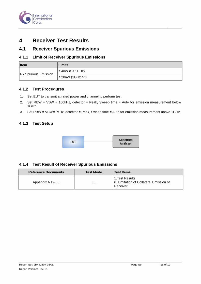
4.1.3 Test Setup
4.1.4 Test Result of Receiver Spurious Emissions
Reference Documents Test Mode Test Items
Appendix A 19-LE LE 1.Test Results 6. Limitation of Collateral Emission of Receiver
Report No.: JR442807-03AE Page No. : 17 of 19
Report Version: Rev. 01
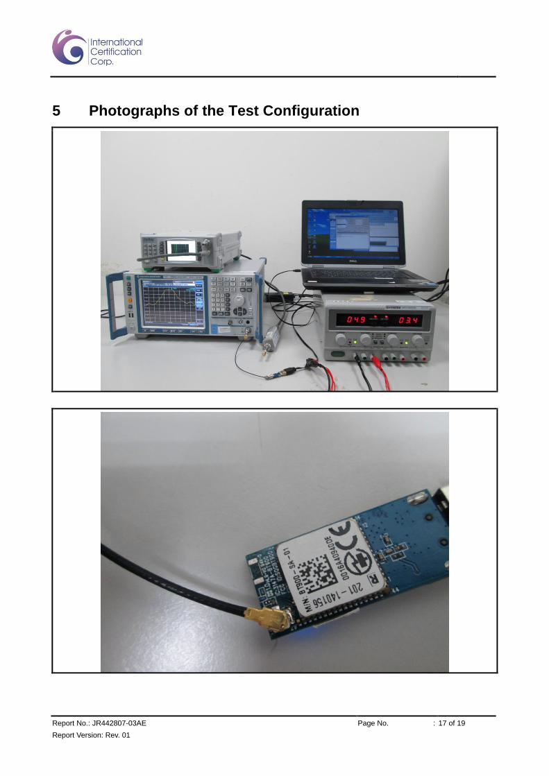
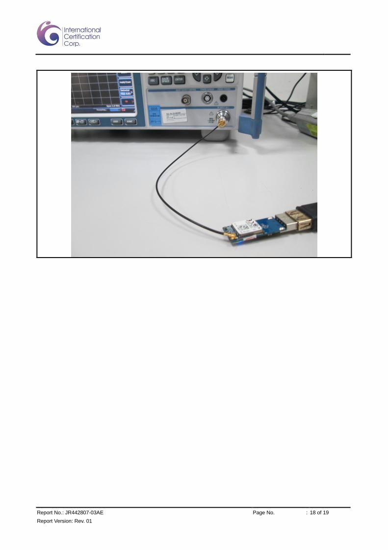
5 Photographs of the Test Configuration
Report No.: JR442807-03AE Page No. : 18 of 19
Report Version: Rev. 01

Report No.: JR442807-03AE Page No. : 19 of 19
Report Version: Rev. 01
6 Test laboratory information
Established in 2012, ICC provides foremost EMC & RF Testing and advisory consultation services by our
skilled engineers and technicians. Our services employ a wide variety of advanced edge test equipment and
one of the widest certification extents in the business.
International Certification Corp, it is our definitive objective is to institute long term, trust-based associations
with our clients. The expectation we set up with our clients is based on outstanding service, practical expertise
and devotion to a certified value structure. Our passion is to grant our clients with best EMC / RF services by
oriented knowledgeable and accommodating staff.
Our Test sites are located at Linkou District and Kwei Shan Hsiang. Location map can be found on our
website http://www.icertifi.com.tw.
Linkou Kwei Shan Kwei Shan Site II
Tel: 886-2-2601-1640 Tel: 886-3-271-8666 Tel: 886-3-271-8640
No. 30-2, Ding Fwu Tsuen, Lin Kou District, New Taipei City, Taiwan, R.O.C.
No. 3-1, Lane 6, Wen San 3rd St., Kwei Shan Hsiang, Tao Yuan Hsien 333, Taiwan, R.O.C.
No. 14-1, Lane 19, Wen San 3rd St., Kwei Shan Hsiang, Tao Yuan Hsien 333, Taiwan, R.O.C.
If you have any suggestion, please feel free to contact us as below information
Tel: 886-3-271-8666
Fax: 886-3-318-0155
Email: [email protected]
END
International Ceritification Corp.
Appendix A - Page A1
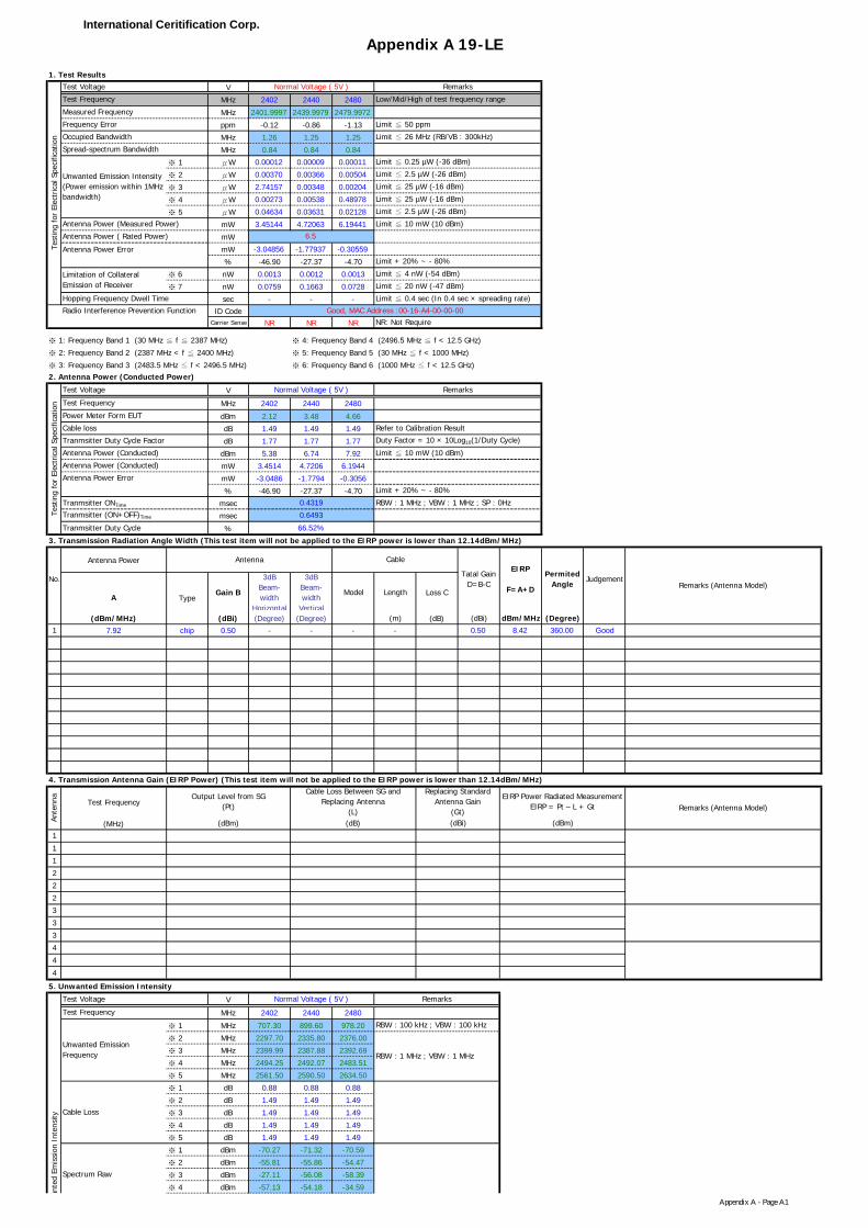
V
MHz 2402 2440 2480
MHz 2401.9997 2439.9979 2479.9972
ppm -0.12 -0.86 -1.13
MHz 1.26 1.25 1.25
MHz 0.84 0.84 0.84
※ 1 μW 0.00012 0.00009 0.00011
※ 2 μW 0.00370 0.00366 0.00504
※ 3 μW 2.74157 0.00348 0.00204
※ 4 μW 0.00273 0.00538 0.48978
※ 5 μW 0.04634 0.03631 0.02128
mW 3.45144 4.72063 6.19441
mW
Antenna Power Error mW -3.04856 -1.77937 -0.30559
% -46.90 -27.37 -4.70
※ 6 nW 0.0013 0.0012 0.0013
※ 7 nW 0.0759 0.1663 0.0728
sec - - -
ID CodeCarrier Sense NR NR NR
※ 1: Frequency Band 1 (30 MHz ≦ f ≦ 2387 MHz) ※ 4: Frequency Band 4 (2496.5 MHz ≦ f < 12.5 GHz)
※ 2: Frequency Band 2 (2387 MHz < f ≦ 2400 MHz) ※ 5: Frequency Band 5 (30 MHz ≦ f < 1000 MHz)
※ 3: Frequency Band 3 (2483.5 MHz ≦ f < 2496.5 MHz) ※ 6: Frequency Band 6 (1000 MHz ≦ f < 12.5 GHz)
V
MHz 2402 2440 2480
dBm 2.12 3.48 4.66
dB 1.49 1.49 1.49
dB 1.77 1.77 1.77
dBm 5.38 6.74 7.92
mW 3.4514 4.7206 6.1944
mW -3.0486 -1.7794 -0.3056
% -46.90 -27.37 -4.70Tranmsitter ONTime msec
msec
%
Antenna Power
AGain B
3dBBeam-width
Horizontal
3dBBeam-width
Vertical
Model Length Loss C
(dBm/MHz) (dBi) (Degree) (Degree) (m) (dB) (dBi) (dBm/MHz) (Degree)1 7.92 chip 0.50 - - - - 0.50 8.42 360.00 Good
Test Frequency
(MHz)111222333444
V
MHz 2402 2440 2480
※ 1 MHz 707.30 899.60 978.20
※ 2 MHz 2297.70 2335.80 2376.00
※ 3 MHz 2399.99 2387.88 2392.69
※ 4 MHz 2494.25 2492.07 2483.51
※ 5 MHz 2561.50 2590.50 2634.50
※ 1 dB 0.88 0.88 0.88
※ 2 dB 1.49 1.49 1.49
※ 3 dB 1.49 1.49 1.49
※ 4 dB 1.49 1.49 1.49
※ 5 dB 1.49 1.49 1.49
※ 1 dBm -70.27 -71.32 -70.59
※ 2 dBm -55.81 -55.86 -54.47
※ 3 dBm -27.11 -56.08 -58.39
※ 4 dBm -57.13 -54.18 -34.59
Antenna Power ( Rated Power)
66.52%
RBW : 1 MHz ; VBW : 1 MHz
PermitedAngle
Judgement
3. Transmission Radiation Angle Width (This test item will not be applied to the EIRP power is lower than 12.14dBm/MHz)
Tranmsitter Duty Cycle
No.Tatal Gain
D=B-C
RBW : 1 MHz ; VBW : 1 MHz ; SP : 0Hz
(dBm)
0.4319
0.6493
Antenna
4. Transmission Antenna Gain (EIRP Power) (This test item will not be applied to the EIRP power is lower than 12.14dBm/MHz)
5. Unwanted Emission Intensity
ante
d Em
issi
on I
nten
sity
Test Voltage Normal Voltage ( 5V ) Remarks
Test Frequency
Unwanted EmissionFrequency
Radio Interference Prevention Function
Measured Frequency
Ante
nna
Limit ≦ 0.4 sec (In 0.4 sec × spreading rate)
Limit ≦ 26 MHz (RB/VB : 300kHz)
Limit + 20% ~ - 80%
Refer to Calibration Result
Limit ≦ 2.5 µW (-26 dBm)
Limit ≦ 4 nW (-54 dBm)
NR: Not Require
Duty Factor = 10 × 10Log10(1/Duty Cycle)
Limit ≦ 20 nW (-47 dBm)
Limit ≦ 2.5 µW (-26 dBm)
Limit ≦ 25 µW (-16 dBm)
Good, MAC Address :00-16-A4-00-00-00
Remarks
Limit ≦ 0.25 µW (-36 dBm)
Unwanted Emission Intensity(Power emission within 1MHzbandwidth)
1. Test Results
Appendix A 19-LE
Test Frequency
Frequency Error
Remarks
Low/Mid/High of test frequency range
Limit ≦ 50 ppm
Test Voltage
Cable loss
Limit ≦ 10 mW (10 dBm)
Antenna Power (Conducted)
Occupied Bandwidth
Limitation of CollateralEmission of Receiver
Hopping Frequency Dwell Time
Limit ≦ 25 µW (-16 dBm)
Test Frequency
Spread-spectrum Bandwidth
Tranmsitter (ON+OFF)Time
Antenna Power (Measured Power)
EIRP
F=A+D
Power Meter Form EUT
Normal Voltage ( 5V )
2. Antenna Power (Conducted Power)
Test
ing
for
Elec
tric
al S
peci
ficat
ion
Test
ing
for
Elec
tric
al S
peci
ficat
ion
Test Voltage Normal Voltage ( 5V )
Tranmsitter Duty Cycle Factor
Antenna Power (Conducted)
Antenna Power Error
Limit + 20% ~ - 80%
Limit ≦ 10 mW (10 dBm)
Remarks (Antenna Model)EIRP Power Radiated Measurement
EIRP = Pt – L + Gt
Remarks (Antenna Model)
Cable
Type
Replacing StandardAntenna Gain
(Gt)(dBi)
Output Level from SG(Pt)
Cable Loss Between SG andReplacing Antenna
(L)(dB)(dBm)
6.5
RBW : 100 kHz ; VBW : 100 kHz
Cable Loss
Spectrum Raw

International Ceritification Corp.
Appendix A - Page A2
※ 5 dBm -44.83 -45.89 -48.21
※ 1 dBm -69.39 -70.44 -69.71
※ 2 dBm -54.32 -54.37 -52.98
※ 3 dBm -25.62 -54.59 -56.90
※ 4 dBm -55.64 -52.69 -33.10
※ 5 dBm -43.34 -44.40 -46.72
※ 1 μW 0.0001 0.0001 0.0001
※ 2 μW 0.0037 0.0037 0.0050
※ 3 μW 2.7416 0.0035 0.0020
※ 4 μW 0.0027 0.0054 0.4898
※ 5 μW 0.0463 0.0363 0.0213
※ 1: Frequency Band 1 (30 MHz ≦ f ≦ 2387 MHz) ※ 4: Frequency Band 4 (2496.5 MHz ≦ f < 12.5 GHz)
※ 2: Frequency Band 2 (2387 MHz < f ≦ 2400 MHz) ※ 5: Frequency Band 5 (30 MHz ≦ f < 1000 MHz)
※ 3: Frequency Band 3 (2483.5 MHz ≦ f < 2496.5 MHz) ※ 6: Frequency Band 6 (1000 MHz ≦ f < 12.5 GHz)
V
MHz 2402 2440 2480
※ 6 MHz 776.10 774.70 776.10 1st
※ 6 MHz - - - 2nd
※ 6 MHz - - - 3rd
※ 7 MHz 6650.00 10511.00 6950.00 1st
※ 7 MHz - - - 2nd
※ 7 MHz - - - 3rd
※ 6 dB 0.88 0.88 0.88 1st
※ 6 dB - - - 2nd
※ 6 dB - - - 3rd
※ 7 dB 1.76 5.68 1.76 1st
※ 7 dB - - - 2nd
※ 7 dB - - - 3rd
※ 6 dBm -89.78 -89.98 -89.64 1st
※ 6 dBm - - - 2nd
※ 6 dBm - - - 3rd
※ 7 dBm -72.96 -73.47 -73.14 1st
※ 7 dBm - - - 2nd
※ 7 dBm - - - 3rd
※ 6 dBm -88.90 -89.10 -88.76 1st
※ 6 dBm - - - 2nd
※ 6 dBm - - - 3rd
※ 7 dBm -71.20 -67.79 -71.38 1st
※ 7 dBm - - - 2nd
※ 7 dBm - - - 3rd
※ 6 nW 0.0013 0.0012 0.0013
※ 6 nW 0.0013 0.0012 0.0013 1st
※ 6 nW - - 2nd
※ 6 nW - - - 3rd
※ 7 nW 0.0759 0.1663 0.0728
※ 7 nW 0.0759 0.1663 0.0728 1st
※ 7 nW - - - 2nd
※ 7 nW - - - 3rd
※ 1: Frequency Band 1 (30 MHz ≦ f ≦ 2387 MHz) ※ 4: Frequency Band 4 (2496.5 MHz ≦ f < 12.5 GHz)
※ 2: Frequency Band 2 (2387 MHz < f ≦ 2400 MHz) ※ 5: Frequency Band 5 (30 MHz ≦ f < 1000 MHz)
※ 3: Frequency Band 3 (2483.5 MHz ≦ f < 2496.5 MHz) ※ 6: Frequency Band 6 (1000 MHz ≦ f < 12.5 GHz)
Limit ≦ 4 nW (-54 dBm)RBW : 100 kHz ; VBW : 100 kHz
Total Emission Power
Limit ≦ 20 nW (-47 dBm)RBW : 1 MHz ; VBW : 1 MHz
Limit ≦ 4 nW (-54 dBm)RBW : 100 kHz ; VBW : 100 kHz
Limit ≦ 20 nW (-47 dBm)RBW : 1 MHz ; VBW : 1 MHz
Total Emission Power
Lim
itatio
n of
Col
late
ral E
mis
sion
Spurious Emission Intensity
Spurious Emission Intensity
Test Frequency30MHz~1000MHz:: Maximumemission and all emissions beyond1/10 of the limitation must beindicated.
Spectrum Raw
Remarks
1000MHz~12.5GHz:: Maximumemission and all emissions beyond1/10 of the limitation must beindicated.
Cable Loss
Normal Voltage ( 5V )
Spurious Emission Frequency
Test Voltage
6. Limitation of Collateral Emission of Receiver
Unw
a
Limit ≦ 25 µW (-16 dBm)
Limit ≦ 2.5 µW (-26 dBm)
Limit ≦ 2.5 µW (-26 dBm)
Limit ≦ 25 µW (-16 dBm)
Limit ≦ 25 µW (-16 dBm)
Limit ≦ 25 µW (-16 dBm)
Limit ≦ 2.5 µW (-26 dBm)
Limit ≦0.25 µW (-36 dBm)
Unwanted Emission Intensity
Unwanted Emission Intensity
Limit ≦0.25 µW (-36 dBm)
Limit ≦ 2.5 µW (-26 dBm)
International Ceritification Corp.
Appendix A - Page A3
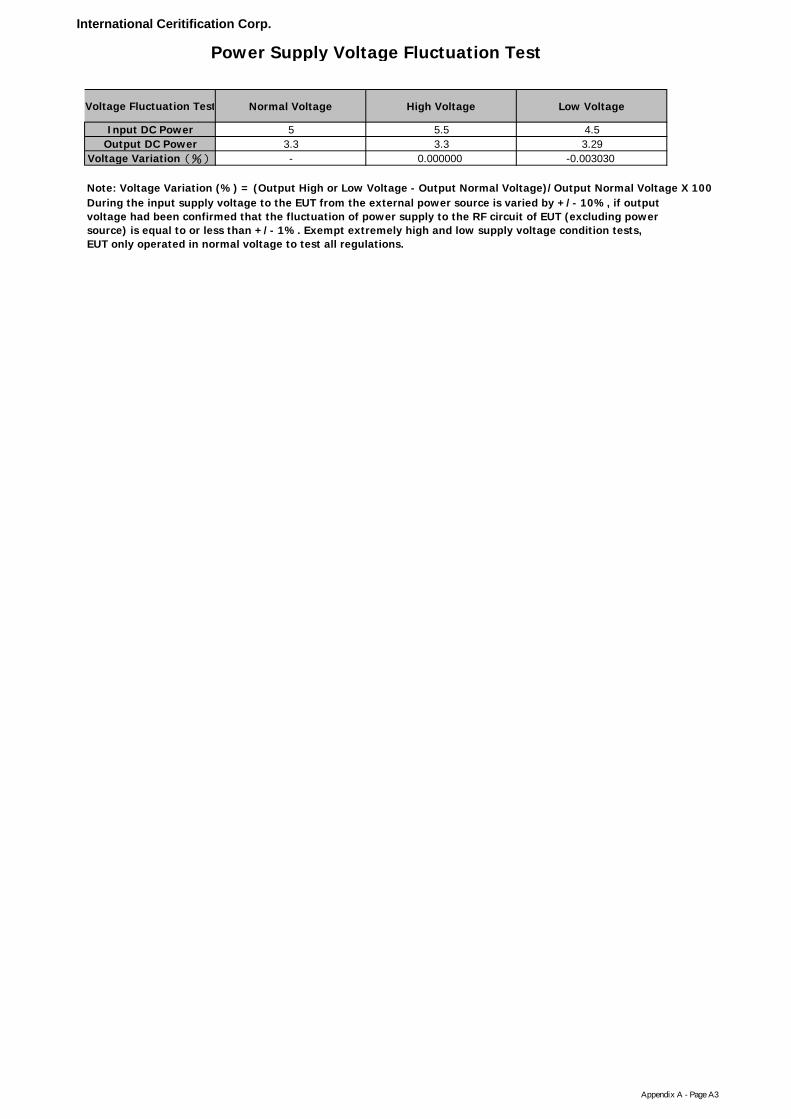
Voltage Fluctuation Test Normal Voltage High Voltage Low Voltage
Input DC Power 5 5.5 4.5Output DC Power 3.3 3.3 3.29
Voltage Variation(%) - 0.000000 -0.003030
Note: Voltage Variation (%) = (Output High or Low Voltage - Output Normal Voltage)/Output Normal Voltage X 100
Power Supply Voltage Fluctuation Test
During the input supply voltage to the EUT from the external power source is varied by +/- 10%, if outputvoltage had been confirmed that the fluctuation of power supply to the RF circuit of EUT (excluding powersource) is equal to or less than +/- 1%. Exempt extremely high and low supply voltage condition tests,EUT only operated in normal voltage to test all regulations.

International Ceritification Corp.
Appendix A - Page A4
1. Linearity Check
SG Output Spectrum Raw Power Meter Raw(dBm) (dBm) (dBm)
0 -1.3 -0.93-5 -6.34 -5.88-10 -11.17 -10.840 -1.64 -1.66-5 -6.6 -6.62-10 -11.48 -11.58
2. Frequency Accuracy Confirmation
SG Output Spectrum Raw Freqquency Error(dBm) (MHz) (ppm)2450 2450.0002 0.08165250 5250.0012 0.2286
3. Cable Loss
SG Output Power Meter Raw Power Meter Raw Cable LossWithout Cable With Cable
(MHz) (dBm) (dBm) (dB)1000 -0.23 -1.11 0.882450 -0.87 -2.36 1.495250 -1.67 -3.43 1.7612500 -3.69 -9.37 5.6826000 -5.55 -19.13 13.58
4. Power Measurement System Loss (EUT Output to IF Output of Spectrum)
SG Output Spectrum Raw Power Meter Raw System Path LossWith Cable form IF EUT to IF
(MHz) (dBm) (dBm) (dB)2450 -1.03 -20.58 19.715250 -5.39 -22.01 20.34
・SG : 0 dBm・RBW : 1 MHz ; VBW : 1 MHz ; SP : 0Hz・ATT(30dB) ; Ref : 20 dBm
Remark
Remark
Remark
Calibration Result
・SG Output : 0dBm・RWB : 30 kHz ; VBW : 30 kHz : SP : 300kHz・Limit ≦ 10% of frequency error limits
・SG Output : 0dBm
・SG Test Frequency : 2450 MHz・RBW : 1 MHz ; VBW : 1 MHz ; SP : 0Hz・ATT(30dB) ; Ref : 20 dBm
Remark
・SG Test Frequency : 5250 MHz・RBW : 1 MHz ; VBW : 1 MHz ; SP : 0Hz・ATT(30dB) ; Ref : 20 dBm

Appendix B. Antenna Information
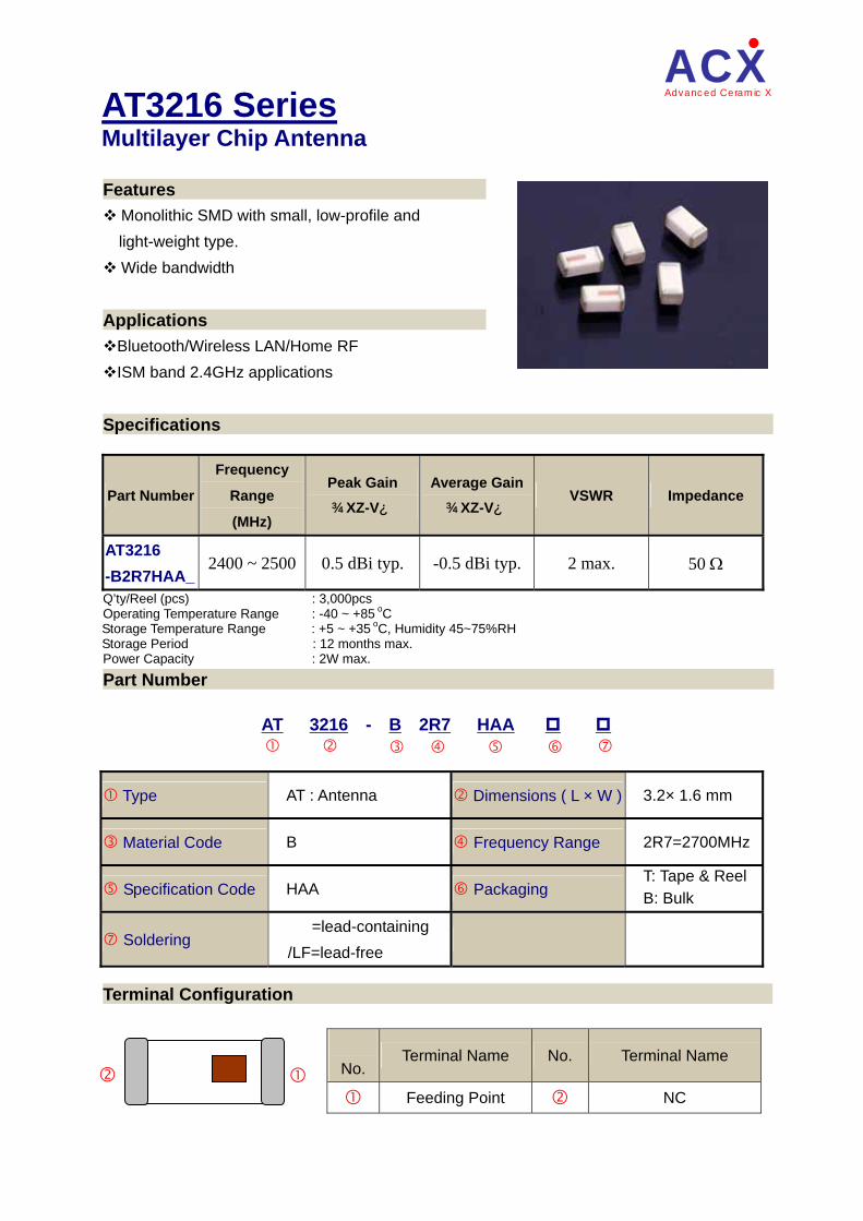
ACX Advanced Ceramic X
Features
Monolithic SMD with small, low-profile and light-weight type. Wide bandwidth
Applications Bluetooth/Wireless LAN/Home RF ISM band 2.4GHz applications
Specifications
Part Number
Frequency
Range
(MHz)
Peak Gain (XZ-V)
Average Gain(XZ-V)
VSWR Impedance
AT3216 -B2R7HAA_
2400 ~ 2500 0.5 dBi typ. -0.5 dBi typ. 2 max. 50 Ω
Q’ty/Reel (pcs) : 3,000pcs Operating Temperature Range : -40 ~ +85 oC Storage Temperature Range : +5 ~ +35 oC, Humidity 45~75%RH Storage Period : 12 months max. Power Capacity : 2W max.
Part Number
Type AT : Antenna Dimensions ( L × W ) 3.2× 1.6 mm
Material Code B Frequency Range 2R7=2700MHz
Specification Code HAA Packaging T: Tape & Reel B: Bulk
Soldering =lead-containing /LF=lead-free
Terminal Configuration
No.
Terminal Name No. Terminal Name
Feeding Point NC
AT3216 Series Multilayer Chip Antenna
AT 3216 - B 2R7 HAA
ACX Advanced Ceramic X
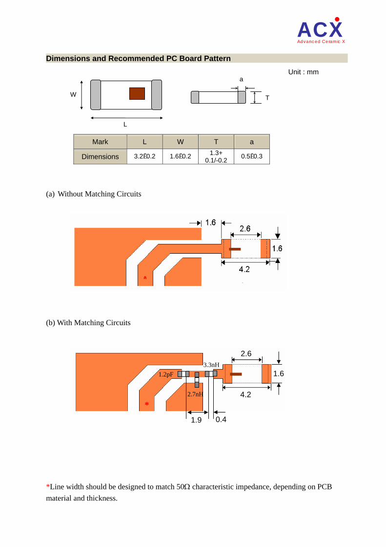
Dimensions and Recommended PC Board Pattern
Mark L W T a
Dimensions 3.2±0.2 1.6±0.2 1.3+ 0.1/-0.2 0.5±0.3
(a) Without Matching Circuits
(b) With Matching Circuits
*Line width should be designed to match 50Ω characteristic impedance, depending on PCB material and thickness.
*
2.6
4.2
1.6
1.9 0.4
Unit : mm
L
W
a
T
3.3nH
2.7nH
1.2pF

ACX Advanced Ceramic X
Typical Electrical Characteristics (T=25oC) Test Board
Return Loss (a) Without Matching Circuits (b) With Matching Circuits
Ground
13.5mm
6.5mm
39.5mm
6.5mm
Matching Circuit
No Ground
50Ω Feed Line
Antenna
19mm
4mm

ACX Advanced Ceramic X
Radiation Patterns
….
XZ cut @2.45GHz Vertical Horizontal
YZ cut @2.45GHz Vertical Horizontal
XZ-V/XZ-H
YZ-V/YZ-H
XY cut @2.45GHz Vertical Horizontal
XY-V/XY-H
Advanced Ceramic X Corp. 16 Tzu Chiang Road, Hsinchu Industrial District Hsinchu Hsien 303, Taiwan TEL:886-3-5987008 FAX:886-3-5987001 E-mail: [email protected] http://www.acxc.com.tw
180o
270o
0o
90o X
Z
Y
XY-cut scanning direction
180o
270o
0o
90o
X
Z
Y
XZ-cut scanning direction
180o
270o
0o
90o
X
Z
Y
YZ-cut scanning direction
![Services & Supportdl.cdn-anritsu.com/en-us/test-measurement/files/Software/... · 2020. 9. 15. · -> Software - SPA and Sub-apps [SPH-283] VBW set to correct bandwidth in Zero Span](https://img.pdfslide.us/doc/110x75/603cb78da7f5512bfe035f37/services-2020-9-15-software-spa-and-sub-apps-sph-283-vbw-set.jpg)