Embed Size (px)
Citation preview

Journal of Theoretical and Applied Information Technology 10
th November 2014. Vol. 69 No.1
© 2005 - 2014 JATIT & LLS. All rights reserved.
ISSN: 1992-8645 www.jatit.org E-ISSN: 1817-3195
8
ANALYSIS OF DC-DC CONVERTER WITH MULTIPLIER
CELLS FOR HIGH VOLTAGE GENERATION
1K.J ANOOP,
2SAPAM ROSHINI DEVI,
3Dr. V.RAJINI
1 Associate Professor, Saveetha School of Engineering, EEE Department, Member, IEEE 2Student, EEE Department, Saveetha School of Engineering
3Professor, Department of EEE, SSN College of Engineering Email: 1 [email protected], 2 [email protected] , 3 [email protected]
ABSTRACT
This paper emphasizes the design of a DC-DC converter to produce high voltage from a low input DC voltage by using multiplier cells instead of a transformer. The low input DC voltage is converted to AC with the help of four switches operating in two different frequencies. Further, this AC voltage is given to the voltage multiplier cells for desired high output DC voltage. The output DC voltage produced has high efficiency, high voltage gain, low ripple, low switching losses and less noise. Two independent frequencies operate in this system, one is known as modulating frequency and the other is alternating frequency which work in high level and low level respectively. A prototype of the proposed model is constructed and the output is compared with the simulated model. The model is again reconstructed by a feedback control for constant output with variable input voltages.
Keywords: Voltage Multiplier, Multilevel Inverter, DC-DC Converter, High Voltage Gain, feedback
Controller
1. INTRODUCTION
Renewable energy methods such as solar, wind, fuel cell etc., are being developed nowadays as they are inexpensive and powerful energy sources [1], [2]. Since the voltage generated from these sources are rather low level, boost converters or transformers are required for high output voltage [3], [4]. Unlike transformers, DC- DC Converters eliminates the requirement of the heavy core, the bulk of insulation and high leakage reactance. Without using the transformers, there are many types of dc-dc boost converters that can be used for increasing the voltage level of the system.
The use of high step up dc-dc converters and
the voltage multipliers have been increasing in industries due to its advantages. Most of the time, they are used in order to produce a high output voltage from a low voltage source and always increase the system efficiency. These types of converters are applicable in the high intensity discharge lamp ballasts, battery backup systems for uninterruptible power supplies and widely used in the renewable energy applications such as fuel-cell energy-conversion systems[5]- [8]. High step up dc-dc converters are important because the system requires a sufficiently high step up conversion with
high efficiency. Theoretically, the boost converter can provide a high step up voltage gain with an extremely high duty cycle [9]-[12].
In the proposed system, the voltage multipliers
are used to produce a high potential dc voltage from a lower voltage ac source. The voltage multiplier can be divided as voltage doublers, triplers, quadruplers etc. The classification depends on the ratio of output voltage to the input voltage. The proposed system using voltage multipliers which is known as Cockcroft-Walton (CW) voltage multiplier to increase the output voltage level and also having the ratio of output voltages to input voltage depending on the number of stages.
2. INVESTIGATIONS ON SELECTIVE
CASCADED DC-DC CONVERTERS Here, two Conventional step up dc-dc
converters without transformer with high voltage gain were presented and compared with the proposed topology. An n-stage diode- capacitor multiplier circuit is proposed [13] in Fig. 1(a) for getting high voltage gain. This system has the advantage of increasing the number of stages without disturbing the main circuit. But the stress on the capacitor increase as the stages increases. Fig.1 (b) shows an n-stage cascade boost converter

Journal of Theoretical and Applied Information Technology 10
th November 2014. Vol. 69 No.1
© 2005 - 2014 JATIT & LLS. All rights reserved.
ISSN: 1992-8645 www.jatit.org E-ISSN: 1817-3195
9
which has the advantages similar to the above [14]. However, the voltage stress on the capacitors at the higher stages are more.
(a)
(b)
Figure 1: (a) Diode Capacitor n-Stage Step-Up Multiplier Converter. (b) Boost Converter with
Cascade Voltage Multiplier Cells.
3. PROPOSED CONVERTER WITH
MULTIPLIER CELLS
This paper emphasis the design, simulation and development of a high voltage dc power generation using Cockcroft Walton voltage multiplier cell and also on the study of hardware construction.
Providing the advantages of high voltage ratio, low voltage stress on the diodes and capacitors, compactness, and cost efficiency, the conventional Cockcroft-Walton (CW) voltage multiplier is very popular among high-voltage dc applications [15]. However, the major drawback is that a high ripple voltage appears at the output when a low-frequency (50 or 60 Hz) utility source is used.
Fig. 2 shows the proposed converter with n-
stage CW voltage multiplier boost-type structure. The proposed converter provides higher voltage ratio than that of the conventional CW voltage multiplier. Thus, the proposed converter is suitable for power conversion applications where high voltage gains are desired. The different voltages can be taken out through tapping at every stage of CW voltage multiplier circuit. The advantages of this circuit is that the voltage across each stage of
the cascade is equal to only twice the peak input voltage.
The proposed converter has less switching stresses, switching losses and EMI noise since it operates in continuous conduction mode (CCM).
Figure 2: Proposed Converter with n-Stage CW
Voltage Multiplier.
The proposed converter contains four switches,
in which Sc1 and Sc2 are used to generate an alternating frequency to feed into the Cockcroft Walton voltage multiplier and the inductor energy is controlled by Sm1 and Sm2 to obtain a boost performance. The four switches operate at two different frequencies, which offer a synchronization between the output ripple and system efficiency. The number of semiconductors in the proposed converter is less as compared with some cascaded dc-dc converters for same voltage level.
4. ANALYSIS OF PROPOSED
CONVERTER
The conventional Cockcroft-Walton (CW)
voltage multiplier with three stages is shown in fig.3. A low level voltage source such as battery, solar cell or fuel cell can be given as the input for the proposed system. The boost inductor operates as inverter and produces an a.c output voltage, where this voltage is again given to the voltage multiplier which will increase several time more than the input voltage. It has the ratio of output voltages to input voltage depending on the number of stages. During the operation of the system, the two frequencies, one operate at high frequency and

Journal of Theoretical and Applied Information Technology 10
th November 2014. Vol. 69 No.1
© 2005 - 2014 JATIT & LLS. All rights reserved.
ISSN: 1992-8645 www.jatit.org E-ISSN: 1817-3195
10
another operate relatively at low frequency. This converter comprises of one boost inductor Ls and four switches Sm1, Sm2, Sc1 and Sc2. Sm1 (Sc1) and Sm2 (Sc2) work in opposite mode and the
operating frequencies of and are given as fsm and fsc respectively.
4.1 Principle of Operation
In the proposed system, the output voltage is increased several times more than the input voltage with the help of voltage multiplier. It is assumed that all the circuit elements are ideal and there is no power loss in the system. The output DC voltage produced has high efficiency, high voltage gain, low ripple, low switching losses and less noise.
Figure 3: Proposed Converter with Three Stage CW
Voltage Multiplier Circuit.
Each capacitor voltage in the CW voltage multiplier is given by Vcx = 2⁄ for x=1 (1)
for x=2,3……n
Where, Vcx = voltage of the xth capacitor
= steady-state voltage of For the n-stage CW voltage multiplier, the output voltage is equal to the total voltage of all even capacitors and can be expressed as
= n (2) Substituting equation (2) into equation (1), the above capacitor voltage can be expressed as
V
cx= 2⁄ for x=1 (3)
⁄ for x=2,3……n Where, Vo= steady-state voltage of the output. 4.2 Modes of Operations
The operation of the proposed converter can be divided into two parts according to the polarity of current to the CW circuit. There are positive conducting interval and Negative conducting interval according to the switching positions. The conducting states of the switches are shown in table1.
Table1. Conducting States of four switches.
Conducting States Strategy 1
Strategy 2
dsc dsm Sc1
SSm1 S
0 0 0101 0111
0 1 0110 0110
1 1 1010 1011
1 0 1001 1001
1 1
or or - 1111
0 0
4.2.1 Mode I
Sm1, Sc1 are turned on, and Sm2, Sc2, and all CW diodes are not conducting. The boost inductor is charged by the input DC source, the group of capacitors C1, C3 and C5 are floating, and the group of capacitors C2, C4 and C6 are supply the load as shown in Fig. 4
Figure 4: Mode I operation
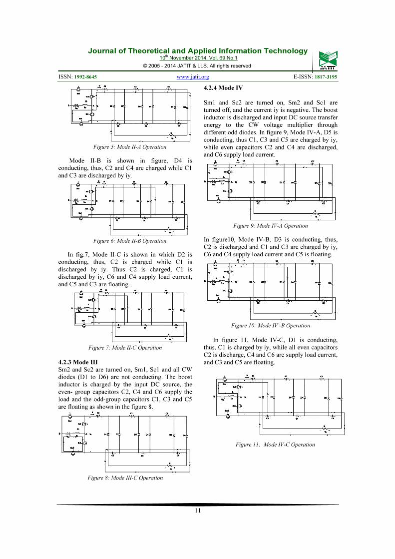
4.2.2 Mode II
Sm2 and Sc1 are turned on. Sm1 and Sc2 are turned off, and the current iy is positive. The boost inductor is discharged and input DC source transfer energy to the CW voltage multiplier through different even diodes. In Mode II-A, D6 is conducting, thus, C2, C4 and C6 are charged while C1, C3 and C5 are discharged by iy. Mode II-A Operation of Proposed Converter is shown in fig. 5.
Journal of Theoretical and Applied Information Technology 10
th November 2014. Vol. 69 No.1
© 2005 - 2014 JATIT & LLS. All rights reserved.
ISSN: 1992-8645 www.jatit.org E-ISSN: 1817-3195
11
Figure 5: Mode II-A Operation
Mode II-B is shown in figure, D4 is conducting, thus, C2 and C4 are charged while C1 and C3 are discharged by iy.
Figure 6: Mode II-B Operation
In fig.7, Mode II-C is shown in which D2 is conducting, thus, C2 is charged while C1 is discharged by iy. Thus C2 is charged, C1 is discharged by iy, C6 and C4 supply load current, and C5 and C3 are floating.
Figure 7: Mode II-C Operation
4.2.3 Mode III
Sm2 and Sc2 are turned on, Sm1, Sc1 and all CW diodes (D1 to D6) are not conducting. The boost inductor is charged by the input DC source, the even- group capacitors C2, C4 and C6 supply the load and the odd-group capacitors C1, C3 and C5 are floating as shown in the figure 8.
Figure 8: Mode III-C Operation
4.2.4 Mode IV
Sm1 and Sc2 are turned on, Sm2 and Sc1 are turned off, and the current iy is negative. The boost inductor is discharged and input DC source transfer energy to the CW voltage multiplier through different odd diodes. In figure 9, Mode IV-A, D5 is conducting, thus C1, C3 and C5 are charged by iy, while even capacitors C2 and C4 are discharged, and C6 supply load current.
Figure 9: Mode IV-A Operation
In figure10, Mode IV-B, D3 is conducting, thus, C2 is discharged and C1 and C3 are charged by iy, C6 and C4 supply load current and C5 is floating.
Figure 10: Mode IV -B Operation
In figure 11, Mode IV-C, D1 is conducting,
thus, C1 is charged by iy, while all even capacitors C2 is discharge, C4 and C6 are supply load current, and C3 and C5 are floating.
Figure 11: Mode IV-C Operation

Journal of Theoretical and Applied Information Technology 10
th November 2014. Vol. 69 No.1
© 2005 - 2014 JATIT & LLS. All rights reserved.
ISSN: 1992-8645 www.jatit.org E-ISSN: 1817-3195
12
5. SIMULATION RESULTS OF PROPOSED
CONVERTER
The proposed model is simulated using MATLAB/Simulink and the specifications for the simulation circuit are given in table 2.
Table 2.Specifications of the Simulation Circuit
Output Voltage 155V
Input DC Voltage 12V
fsm 60kHz
fsc 1kHz
Resistance 1kΩ
Inductance 1.5mH
Capacitance 470µF
Resistive Load 1kΩ
Number of stages, n 3
The comparison of gain in the conventional dc-dc converters and the prosed is shown in figure 12.
Figure 12: Simulated Voltage Gains of the Conventional and Proposed Converter.
The MATLAB/Simulink circuit of the proposed dc-dc converter is given figure 13. Figure 14 shows the switching pulses given to the IGBT switches. The voltage across the switches are shown in figure 15. Sm1, Sm2 works with 1 kHz and Sc1, Sc2 works with 16 kHz frequency. The output voltage waveform of the proposed converter for 0.5 duty cycle with an input voltage of 12V is 138V shown in the figure 16. .
Figure 13: Simulation of the Proposed Converter.
Figure14: Simulation of Gate Switching Pulse
Waveforms to Sm1, Sm2, Sc1 and Sc2 Respectively
Figure 15: Switching Stress across the Switches
Sc1, Sc2, Sm1 and Sm2 Respectively.
Figure 16: Output Voltage of the Proposed Three

Journal of Theoretical and Applied Information Technology 10
th November 2014. Vol. 69 No.1
© 2005 - 2014 JATIT & LLS. All rights reserved.
ISSN: 1992-8645 www.jatit.org E-ISSN: 1817-3195
13
Stage Multiplier Circuit
6. EXPERIMENTAL RESULTS
An open loop prototype was built to verify the validity of the proposed converter is shown in figure17. This circuit can be used for the application of constant output voltage if the input from the battery or renewable energy sources are constant. It operates in continuous conduction mode so that switch stress and the EMI noise can be reduced. It produces high output voltage, high efficiency and low ripple voltage.
Figure 17: Prototype of the Proposed Model (Open
Loop)
The table 3 shows the specifications of the hardware model.
Table 3. Hardware Description
Components Symbol Value
Boost Inductor Ls 1.5mH
Power Switches Sm1,Sm2,Sc1,Sc2 IGBT
Capacitors C1-C6 470µF
The Hardware output voltage is measured using High resolution Digital Storage Oscilloscope (Agilent Technologies) and shown in the figure 18. The output of the Prototype is agreeing with the Simulation output.
Figure 18: Output Voltage of the Prototype
Normally the input voltage from battery or renewable energy sources will not be constant hence, the output voltage also. For getting constant output voltage the prototype is modified with closed loop control is shown in figure19.
Figure19: Prototype of the Proposed Model (Closed
Loop)
The output voltage of three stages of the Cockcroft
Walton Multiplier Circuit with an input of 12V is shown
in figure20.
Figure20: Output Voltage at each Stage of Capacitor

Journal of Theoretical and Applied Information Technology 10
th November 2014. Vol. 69 No.1
© 2005 - 2014 JATIT & LLS. All rights reserved.
ISSN: 1992-8645 www.jatit.org E-ISSN: 1817-3195
14
The closed loop control of the prototype gives same output voltage with another input is shown in figure 21.The input voltage is varied by a potentiometer and the output is noted. The error in the output with the reference is calculated and given the feedback to the switching circuit for getting a constant output voltage.
Figure21: Constant Output Voltage with an Input of
7.85V
7. CONCLUSION
The paper explains a dc-dc converter using Cockcroft Walton Multiplier cells for getting high voltage gain. The stress on the switches, capacitors and diodes are not affected when the number stages increases hence, high voltage can be generated by the proposed model. The analysis, principle of operation and the mode of operation were discussed. The Simulation has been done with MATLAB/Simulink are compared with the experimental results. Obviously, the simulation results well agree with the experimental results. However, the voltage ripple exists practically in all capacitors, the voltage multipliers will increase the low input voltage to high dc output voltage level.
REFERENCES:
[1] B. K. Bose, “Energy, environment, and advances in power electronics,” IEEE
Trans. Power Electron., vol. 15, no. 4, pp. 688–701, Jul. 2000.
[2] F. Blaabjerg, Z. Chen, and S. B. Kjaer, “Power electronics as efficient interface in dispersed power generation systems,” IEEE Trans.
Power Electron., vol. 19, no. 5, pp. 1184–1194, Sep. 2004.
[3] G. R. Walker and P. C. Sernia, “Cascaded dc-dc converter connection of photovoltaic modules,” IEEE Trans. Power Electron., vol. 19, no. 4, pp. 1130–1139, Jul. 2004.
[4] J. Wang, F. Z. Peng, J. Anderson, A.Joseph and R. Buffenbarger, “Low cost fuel cell converter system for residential power generation,” IEEE Trans. Power Electron., vol. 19, no. 5, pp. 1315–1322, Sep. 2004.
[5] M. W. Ellis, M. R. Von Spakovsky, and D. J. Nelson, “Fuel cell systems: Efficient, flexible energy conversion for the 21st century,” Proc. IEEE, vol. 89, no. 12, pp. 1808–1817, Dec. 2001
[6] Q. Li and P. Wolfs, “A review of the single phase photovoltaic module integratedconverter topologies with three different dc link configurations,IEEE Trans.
Power Electron., vol. 23, no. 3, pp. 1320–1333, May 2008.
[7] W. Li and X. He, “Review of nonisolated high-step-up dc/dc converters in photovoltaic grid-connected applications,” IEEE Trans.
Ind. Electron.,vol. 58, no. 4, pp. 1239–1250, Apr. 2011.
[8] L. S. Yang, T. J. Liang, and J. F. Chen, Transformerless dc-dc converterswith high step-up voltage gain,” IEEE Trans. Ind.
Electron., vol. 56, no. 8,pp. 3144–3152, Aug. 2009.
[9] R. J. Wai, C. Y. Lin, C. Y. Lin, R. Y. Duan, and Y. R. Chang, “Highefficiencypower conversion system for kilowatt-level stand-alone generationunit with low input voltage,” IEEE Trans. Ind. Electron., vol. 55,no. 10, pp. 3702–3714, Oct. 2008.
[10] J. M. Kwon, E. H. Kim, B. H. Kwon, and K. H. Nam, “High-efficiency fuel cell power conditioning system with input current ripple reduction,”IEEE Trans. Ind. Electron., vol. 56, no. 3, pp. 826–834, Mar. 2009.
[11] A. K. Rathore, A. K. S. Bhat, and R. Oruganti, “Analysis, design and experimental results of wide range ZVS active-clamped L-L type currentfed dc/dc converter for fuel cells to utility interface,” IEEE Trans.
Ind.Electron., vol. 59, no. 1, pp. 473–485, Jan. 2012.
[12] B. Yuan, X. Yang, X. Zeng, J. Duan, J. Zhai, and D. Li, “Analysis and design of a high step-up current-fed Multiresonant dc/dc converter with low circulating energy and zero-current switching for all active switches,”IEEE Trans. Ind. Electron., vol. 59, no. 2, pp. 964–978, Feb. 2012.
[13] Y. Berkovich, B. Axelrod, and A. Shenkman, “A novel diode-capacitorvoltage multiplier for increasing the voltage of photovoltaic

Journal of Theoretical and Applied Information Technology 10
th November 2014. Vol. 69 No.1
© 2005 - 2014 JATIT & LLS. All rights reserved.
ISSN: 1992-8645 www.jatit.org E-ISSN: 1817-3195
15
cells,” inProc. IEEE COMPEL, Zurich, Switzerland, Aug. 2008, pp. 1–5.
[14] M. Prudente, L. L. Pfitscher, G. Emmendoerfer, E. F. Romaneli, andR. Gules, “Voltage multiplier cells applied to non-isolated dc-dc converters,”IEEE Trans.
Power Electron., vol. 23, no. 2, pp. 871–887,Mar. 2008.
[15] Chung-Ming Young, Ming-Hui Chen, Tsun-An Chang, Chun-Cho Ko and Kuo-Kuang Jen, “Cascade Cockcroft–Walton Voltage Multiplier Applied to Transformerless High Step-Up DC–DC Converter”IEEE Trans. Industrial Electronics., vol. 60, no. 2, pp. 523–537,Feb. 2013.