Embed Size (px)
Citation preview

FN7840Rev.2.00
Sep 8, 2017
ISL976912.4V LED Driver with Independent Analog and PWM Dimming Controls of 2 Backlights for 3D Application
DATASHEET
The ISL97691 is Intersil’s highly integrated 4 channel LED driver for single cell Li-Ion battery operated mobile displays requiring analog dimming, and for 3D mobile display applications. It drives four 40mA channels of LEDs up to 26V from an input supply 2.4V to 5.5V. The ISL97691 will also drive 60mA channels up to 21V at 30% duty for high peak current 3D modes.
The ISL97691 provides 4 channels of current with 2 independent analog dimming controls and 2 independent PWM dimming controls. Channels 1 and 2 form one channel group and channels 3 and 4 form the other channel group. Each channel group’s analog dimming is controlled through 1-Wire communication with 6-bit resolution and each channel group’s PWM dimming is controlled by a separate PWM input. This unique setup allows 2D or 3D application where independent and dynamic channel control of LED peak current and PWM dimming duty cycle are possible. The ISL97691 employs adaptive boost architecture that allows ultra low dimming duty cycle as low as 0.005% at 100Hz dimming frequency.
The driver features dynamic headroom control that monitors the highest LED forward voltage string and uses its feedback signal for the minimum output regulation.
The ISL97691 incorporates extensive protection functions including string open and short circuit detections, OVP, and OTP. The switching frequency can be adjusted from 400kHz to 1.5MHz. The device is offered in a 16 Ld TQFN 3x3mm package and can operate in ambient temperature from -40°C to +85°C.
Features• 2.4V minimum input voltage, no need for higher voltage
supplies
• 4 x 60mA (Note 1) and 4 x 40mA (Note 2) LED current
• 2 groups of independent analog and pwm current controls
- 1-wire interfaces for 6-bit analog dimming
- PWM inputs for PWM dimming
- 0.005% minimum PWM dimming duty cycle at 100Hz
• Low 0.8mA quiescent current
• ±2.5% current matching
• Adjustable switching frequency from 400kHz to 1.5MHz
• Fault protection
- OVP, OTP, channel open/short circuit protections
NOTES:
1. Not exceeding 30% of the frame rate (1/tFRAME), with VIN > 2.7V and TA < +55°C.
2. VIN > 2.7V
Applications• Tablet, notebook PC, and smart phone displays LED
backlighting
• Mobile displays for 2D or 3D LED backlighting
Related Literature• For a full list of related documents, visit our website
- ISL97691 product page
I
FIGURE 1. TYPICAL APPLICATION CIRCUIT FIGURE 2. ULTRA LOW PWM DIMMING LINEARITY
FSW
AGND
OVP
VIN
1-WIRE_1
ISET
COMP
D1
CH1
CH2
CH3
CH4
PGND
LX
VIN = 2.7V~5.5V VOUT = 24.5V, 4 x 60mA*L1
10µH
12k
15nF
10
1µF
4.7µF4.7µF
470k
23.7k
143k
17.8k
100pF
2.2nFISL97691
4.7µF
1-WIRE_2
*NOT EXCEEDING 30% PWM DUTY
PWM2
PWM_1
0.0001
0.001
0.01
0.1
1
10
0.001 0.01 0.1 1 10
INPUT DIMMING DUTY CYCLE (%)
ILE
D (
mA
)
fPWM: 200Hz
fPWM: 100Hz
FN7840 Rev.2.00 Page 1 of 19Sep 8, 2017

ISL97691
Block Diagram
REFGEN
VIN
GMAMP
CH1
CH4
PWM/PFM
LOGIC
FET
DRIVERS
OVPREG
OSC & RAMP COMP
IMAX
HIGHEST VF STRING
DETECT
TEMPSENSOR
ISET
+-
O/P SHORT
REF_OVP REF_VSC
INTERNAL BIAS
OPEN CKT, SHORT CKT DETECTION
DYNAMIC HEADROOM CONTROL
OVP
FSW
PWMI_1PWM DIMMING CONTROLLER
UP TO 26V
LX
VIN = 2.4V~5.5V
PWMI_2
10µH
ISL97691
CH2CH3
PGND
2X4.7µF
ILIMIT
S = 0
DC1
PWM1
+-
1
+-
2
PWM2
+-
3
+-
4
8-BIT DAC
6-BIT DAC
DC26-BIT DAC
1-WIRE I/F1-WIRE_11-WIRE_2
COMP
Ordering InformationPART NUMBER(Notes 3, 4, 5)
PART MARKING
TEMP RANGE(°C)
PACKAGE(RoHS COMPLIANT)
PKG. DWG. #
ISL97691IRTZ 7691 -40 to +85 16 Ld TQFN L16.3x3D
ISL97691IRTZ-EVALZ Evaluation Board
NOTES:
3. Add “-T” suffix for 6k unit or “-TK” suffix for 1k unit tape and reel. Refer to TB347 for details on reel specifications.
4. These Intersil Pb-free plastic packaged products employ special Pb-free material sets; molding compounds/die attach materials and 100% matte tin plate - e3 termination finish, which is RoHS compliant and compatible with both SnPb and Pb-free soldering operations. Intersil Pb-free products are MSL classified at Pb-free peak reflow temperatures that meet or exceed the Pb-free requirements of IPC/JEDEC J STD-020.
5. For Moisture Sensitivity Level (MSL), see the product information page for ISL97691. For more information on MSL see TB363.
FN7840 Rev.2.00 Page 2 of 19Sep 8, 2017

ISL97691
Pin ConfigurationISL97691
(16 LD 3mmx3mm TQFN )TOP VIEW
Pin DescriptionPIN NUMBER PIN NAME I/O DESCRIPTION
1 AGND S Analog Ground for precision circuits.
2 COMP I External compensation. Fit a series RC comprising 12kΩ and 15nF from COMP to GND.
3 ISET I Channel current setting. The LED channel current is adjusted from 15mA to 60mA with resistor RSET from ISET pin to GND.
4 1-WIRE_1 I 1-Wire interface 1 for controlling channels 1 and 2 with 6-bit analog dimming.
5 1-WIRE_2 I 1-Wire interface 2 for controlling channels 3 and 4 with 6-bit analog dimming.
6 PWMI_1 I PWM Input 1 for controlling channels 1 and 2 PWM dimming. During the PWM Off period, the 1-WIRE_1 data will remain at the previous programmed level.
7 PWMI_2 I PWM Input 2 for controlling channels 3 and 4 PWM dimming. During the PWM Off period, the 1-WIRE_2 data will remain at the previous programmed level.
8 VIN I Input supply voltage.
9 LX O Input to boost switch.
10 PGND S Power ground (LX, CIN, and COUT power return).
11 FSW I Switching Frequency Adjustment. The boost switching frequency is adjusted from 400kHz to 1.5MHz with resistor RFSW from FSW pin to GND.
12 OVP I Overvoltage protection input.
13 CH1 I Channel 1 current sink and channel monitoring. Tie pin to GND if channel unused.
14 CH2 I Channel 2 current sink and channel monitoring. Tie pin to GND if channel unused.
15 CH3 I Channel 3 current sink and channel monitoring. Tie pin to GND if channel unused.
16 CH4 I Channel 4 current sink and channel monitoring. Tie pin to GND if channel unused.
EPAD X No electrical connection but should be used to connect PGND and AGND. For example, uses top plane as PGND and bottom plane as AGND with vias on EPAD to allow heat dissipation and minimum noise coupling from PGND to AGND operation.
1
3
4
15
AGND
COMP
ISET
1-WIRE_1
CH
4
CH
3
CH
2
CH
1
16 14 13
2
12
10
9
11
65 7 8
OVP
FSW
PGND
LX
1-W
IRE
_2
PW
MI_
2
EN
/PW
MI_
2
VIN
THERMAL PAD
FN7840 Rev.2.00 Page 3 of 19Sep 8, 2017

ISL97691
Table of ContentsAbsolute Maximum Ratings . . . . . . . . . . . . . . . . . . . . . . . . . . . . . . . . . . . . . . . . . . . . . . . . . . . . . . . . . . . . . . . . . . . . . . . . . . . . . . . . . . . 5
Thermal Information . . . . . . . . . . . . . . . . . . . . . . . . . . . . . . . . . . . . . . . . . . . . . . . . . . . . . . . . . . . . . . . . . . . . . . . . . . . . . . . . . . . . . . . . . 5
Operating Conditions . . . . . . . . . . . . . . . . . . . . . . . . . . . . . . . . . . . . . . . . . . . . . . . . . . . . . . . . . . . . . . . . . . . . . . . . . . . . . . . . . . . . . . . . 5
Electrical Specifications . . . . . . . . . . . . . . . . . . . . . . . . . . . . . . . . . . . . . . . . . . . . . . . . . . . . . . . . . . . . . . . . . . . . . . . . . . . . . . . . . . . . . . . . . . . . . . 5
Typical Performance Curves . . . . . . . . . . . . . . . . . . . . . . . . . . . . . . . . . . . . . . . . . . . . . . . . . . . . . . . . . . . . . . . . . . . . . . . . . . . . . . . . . . 8
Theory of Operation. . . . . . . . . . . . . . . . . . . . . . . . . . . . . . . . . . . . . . . . . . . . . . . . . . . . . . . . . . . . . . . . . . . . . . . . . . . . . . . . . . . . . . . . . 11
PWM Boost Converter . . . . . . . . . . . . . . . . . . . . . . . . . . . . . . . . . . . . . . . . . . . . . . . . . . . . . . . . . . . . . . . . . . . . . . . . . . . . . . . . . . . . . . . . . . . . 11AutoShutdown . . . . . . . . . . . . . . . . . . . . . . . . . . . . . . . . . . . . . . . . . . . . . . . . . . . . . . . . . . . . . . . . . . . . . . . . . . . . . . . . . . . . . . . . . . . . . . . . . . 11Dimming Controls . . . . . . . . . . . . . . . . . . . . . . . . . . . . . . . . . . . . . . . . . . . . . . . . . . . . . . . . . . . . . . . . . . . . . . . . . . . . . . . . . . . . . . . . . . . . . . . 11
ANALOG Dimming . . . . . . . . . . . . . . . . . . . . . . . . . . . . . . . . . . . . . . . . . . . . . . . . . . . . . . . . . . . . . . . . . . . . . . . . . . . . . . . . . . . . . . . . . . . . 11PWM Dimming . . . . . . . . . . . . . . . . . . . . . . . . . . . . . . . . . . . . . . . . . . . . . . . . . . . . . . . . . . . . . . . . . . . . . . . . . . . . . . . . . . . . . . . . . . . . . . 12
Current Matching and Current Accuracy. . . . . . . . . . . . . . . . . . . . . . . . . . . . . . . . . . . . . . . . . . . . . . . . . . . . . . . . . . . . . . . . . . . . . . . . . . . . . 12Dynamic Headroom Control . . . . . . . . . . . . . . . . . . . . . . . . . . . . . . . . . . . . . . . . . . . . . . . . . . . . . . . . . . . . . . . . . . . . . . . . . . . . . . . . . . . . . . . 12Soft-Start. . . . . . . . . . . . . . . . . . . . . . . . . . . . . . . . . . . . . . . . . . . . . . . . . . . . . . . . . . . . . . . . . . . . . . . . . . . . . . . . . . . . . . . . . . . . . . . . . . . . . . . 12Power-Off Sequence . . . . . . . . . . . . . . . . . . . . . . . . . . . . . . . . . . . . . . . . . . . . . . . . . . . . . . . . . . . . . . . . . . . . . . . . . . . . . . . . . . . . . . . . . . . . . 12Operation with Input Voltage Greater than 5.5V . . . . . . . . . . . . . . . . . . . . . . . . . . . . . . . . . . . . . . . . . . . . . . . . . . . . . . . . . . . . . . . . . . . . . . . . . . . . . . .12
Component Selection . . . . . . . . . . . . . . . . . . . . . . . . . . . . . . . . . . . . . . . . . . . . . . . . . . . . . . . . . . . . . . . . . . . . . . . . . . . . . . . . . . . . . . . 13
Input Capacitor. . . . . . . . . . . . . . . . . . . . . . . . . . . . . . . . . . . . . . . . . . . . . . . . . . . . . . . . . . . . . . . . . . . . . . . . . . . . . . . . . . . . . . . . . . . . . . . . . . 13Overvoltage Protection (OVP) . . . . . . . . . . . . . . . . . . . . . . . . . . . . . . . . . . . . . . . . . . . . . . . . . . . . . . . . . . . . . . . . . . . . . . . . . . . . . . . . . . . . . . 13Boost Output Voltage Range . . . . . . . . . . . . . . . . . . . . . . . . . . . . . . . . . . . . . . . . . . . . . . . . . . . . . . . . . . . . . . . . . . . . . . . . . . . . . . . . . . . . . . 14Switching Frequency . . . . . . . . . . . . . . . . . . . . . . . . . . . . . . . . . . . . . . . . . . . . . . . . . . . . . . . . . . . . . . . . . . . . . . . . . . . . . . . . . . . . . . . . . . . . . 14Inductor. . . . . . . . . . . . . . . . . . . . . . . . . . . . . . . . . . . . . . . . . . . . . . . . . . . . . . . . . . . . . . . . . . . . . . . . . . . . . . . . . . . . . . . . . . . . . . . . . . . . . . . . 14Schottky Diode . . . . . . . . . . . . . . . . . . . . . . . . . . . . . . . . . . . . . . . . . . . . . . . . . . . . . . . . . . . . . . . . . . . . . . . . . . . . . . . . . . . . . . . . . . . . . . . . . . 14Compensation . . . . . . . . . . . . . . . . . . . . . . . . . . . . . . . . . . . . . . . . . . . . . . . . . . . . . . . . . . . . . . . . . . . . . . . . . . . . . . . . . . . . . . . . . . . . . . . . . . 14
Applications . . . . . . . . . . . . . . . . . . . . . . . . . . . . . . . . . . . . . . . . . . . . . . . . . . . . . . . . . . . . . . . . . . . . . . . . . . . . . . . . . . . . . . . . . . . . . . . 14
Unused LED Channels . . . . . . . . . . . . . . . . . . . . . . . . . . . . . . . . . . . . . . . . . . . . . . . . . . . . . . . . . . . . . . . . . . . . . . . . . . . . . . . . . . . . . . . . . . . . 14High Current Applications . . . . . . . . . . . . . . . . . . . . . . . . . . . . . . . . . . . . . . . . . . . . . . . . . . . . . . . . . . . . . . . . . . . . . . . . . . . . . . . . . . . . . . . . . 14
PCB Layout Considerations . . . . . . . . . . . . . . . . . . . . . . . . . . . . . . . . . . . . . . . . . . . . . . . . . . . . . . . . . . . . . . . . . . . . . . . . . . . . . . . . . . 15
PCB Layout with TQFN Package . . . . . . . . . . . . . . . . . . . . . . . . . . . . . . . . . . . . . . . . . . . . . . . . . . . . . . . . . . . . . . . . . . . . . . . . . . . . . . . . . . . 15General Power PAD Design Considerations . . . . . . . . . . . . . . . . . . . . . . . . . . . . . . . . . . . . . . . . . . . . . . . . . . . . . . . . . . . . . . . . . . . . . . . . . . 15
Fault Protection and Monitoring . . . . . . . . . . . . . . . . . . . . . . . . . . . . . . . . . . . . . . . . . . . . . . . . . . . . . . . . . . . . . . . . . . . . . . . . . . . . . . 16
Short Circuit Protection (SCP) . . . . . . . . . . . . . . . . . . . . . . . . . . . . . . . . . . . . . . . . . . . . . . . . . . . . . . . . . . . . . . . . . . . . . . . . . . . . . . . . . . . . . 16Open Circuit Protection (OCP) . . . . . . . . . . . . . . . . . . . . . . . . . . . . . . . . . . . . . . . . . . . . . . . . . . . . . . . . . . . . . . . . . . . . . . . . . . . . . . . . . . . . . 16Undervoltage Lockout . . . . . . . . . . . . . . . . . . . . . . . . . . . . . . . . . . . . . . . . . . . . . . . . . . . . . . . . . . . . . . . . . . . . . . . . . . . . . . . . . . . . . . . . . . . . 16Over-Temperature Protection (OTP) . . . . . . . . . . . . . . . . . . . . . . . . . . . . . . . . . . . . . . . . . . . . . . . . . . . . . . . . . . . . . . . . . . . . . . . . . . . . . . . . 16
Revision History. . . . . . . . . . . . . . . . . . . . . . . . . . . . . . . . . . . . . . . . . . . . . . . . . . . . . . . . . . . . . . . . . . . . . . . . . . . . . . . . . . . . . . . . . . . . 18
About Intersil . . . . . . . . . . . . . . . . . . . . . . . . . . . . . . . . . . . . . . . . . . . . . . . . . . . . . . . . . . . . . . . . . . . . . . . . . . . . . . . . . . . . . . . . . . . . . . 18
Package Outline Drawing . . . . . . . . . . . . . . . . . . . . . . . . . . . . . . . . . . . . . . . . . . . . . . . . . . . . . . . . . . . . . . . . . . . . . . . . . . . . . . . . . . . . 19
FN7840 Rev.2.00 Page 4 of 19Sep 8, 2017

ISL97691
Absolute Maximum Ratings Thermal InformationVIN, FSW, ISET, COMP, OVP . . . . . . . . . . . . . . . . . . . . . . . . . . . . -0.3V to 5.5VPWMI_1, PWMI_2 . . . . . . . . . . . . . . . . . . . . . . . . . . . . . . . . . . . -0.3V to 5.5V1-WIRE_1, 1-WIRE_2 . . . . . . . . . . . . . . . . . . . . . . . . . . . . . . . . . -0.3V to 5.5VCH1 to CH4, LX . . . . . . . . . . . . . . . . . . . . . . . . . . . . . . . . . . . . . . . -0.3V to 28VPGND, AGND . . . . . . . . . . . . . . . . . . . . . . . . . . . . . . . . . . . . . . . -0.3V to +0.3VAbove voltage ratings are all with respect to AGND pin
ESD RatingsHuman Body Model (Tested per JESD22-A114F) . . . . . . . . . . . . . . .2.5kVMachine Model (Tested per JESD22-A115C) . . . . . . . . . . . . . . . . . . 200VCharged Device Model (JESD22-C101E) . . . . . . . . . . . . . . . . . . . . . . . 2kV
Latch Up (Tested per JESD-78B; Class 2, Level A) . . . . . . . . . . . . . . 100mA
Thermal Resistance (Typical) JA (°C/W) JC (°C/W)16 LD TQFN (Notes 6, 7) . . . . . . . . . . . . . . . 51 4.6
Thermal Characterization (Typical) PSIJT (°C/W)
16 Ld TQFN (Note 8) . . . . . . . . . . . . . . . . . . . . . . . . . . . . 0.11Maximum Continuous Junction Temperature . . . . . . . . . . . . . . . . .+125°CStorage Temperature . . . . . . . . . . . . . . . . . . . . . . . . . . . . .-65°C to +150°C
Operating ConditionsTemperature Range . . . . . . . . . . . . . . . . . . . . . . . . . . . . . . . . -40°C to +85°C
CAUTION: Do not operate at or near the maximum ratings listed for extended periods of time. Exposure to such conditions may adversely impact productreliability and result in failures not covered by warranty.
NOTES:
6. JA is measured in free air with the component mounted on a high effective thermal conductivity test board with “direct attach” features. See TB379.
7. For JC, the “case temp” location is the center of the exposed metal pad on the package underside.
8. PSIJT is the PSI junction-to-top thermal characterization parameter. If the package top temperature can be measured with this rating then the die junction temperature can be estimated more accurately than the JC and JC thermal resistance ratings.
Electrical Specifications All specifications below are characterized at TA = -40°C to +85°C; VIN = 3.3V, PWMI_1 = 3.3V, RISET = 26.7kΩ, unless otherwise noted. Boldface limits apply across the operating temperature range, -40°C to +85°C.
PARAMETER DESCRIPTION CONDITIONMIN
(Note 9) TYPMAX
(Note 9) UNIT
GENERAL
VIN Backlight Supply Voltage TA = +25°C 2.4 5.5 V
IVIN VIN Active Current, All Strings 100% Duty, ILED = 40mA
All channels 100% duty 2.5 mA
All channels 0% duty 0.8 mA
IAUTOSHUTDOWN VIN Shutdown Current, both 1-Wire Interface Inputs Inactive
PWMI_1 and PWMI_2 low longer than tPWMTIMEOUT
1 µA
VOUT Output Voltage VIN 2.7V, ILED = 40mA 26 V
tWAKE Wakeup Time from Sleep Boost and channels operating 1.5 2.2 ms
VUVLO Undervoltage Lockout Threshold 2 2.15 2.35 V
VUVLO_HYS Undervoltage Lockout Hysteresis 150 mV
BOOST SWITCHING REGULATOR
SS Soft-start 100% LED Duty Cycle 7 ms
SWILimit Boost FET Current Limit 2.5 2.8 3.2 A
rDS(ON) Internal Boost Switch ON-Resistance TA = +25°C 212 mΩ
Eff_peak Peak Efficiency VIN = 5.5V, VOUT = 21V, TA = +25°C, RFSW = 144kΩICH1-CH4 = 20mA,L = 10µH with DCR 150mΩ
90 %
VIN = 2.4V, VOUT = 21V, TA = +25°C, RFSW = 144kΩICH1-CH4 = 20mA,L = 10µH with DCR 150mΩ
74 %
DMAX Boost Maximum Duty Cycle FSW = 400kHz 93.5 %
FSW = 1.5MHz 93 %
FN7840 Rev.2.00 Page 5 of 19Sep 8, 2017

ISL97691
DMIN Boost Minimum Duty Cycle FSW = 400kHz 11 %
FSW = 1.5MHz 15 %
fSW Boost Switching Frequency RFSW = 216kΩ 360 400 440 kHz
RFSW = 72.1kΩ 1.2 MHz
RFSW = 57.7kΩ 1.35 1.5 1.65 MHz
ILX_leakage LX Leakage Current LX = 26V 10 µA
REFERENCE
IMATCH Channel-to-Channel DC Current Matching ILED = 20mA -2.5 +2.5 %
IACC Current Accuracy ILED = 20mA -3 +3 %
FAULT DETECTION
VSC Channel Short Circuit Threshold 6.75 8 9.25 V
Vtemp Over-Temperature Threshold 150 °C
VOVPlo Overvoltage Limit on OVP Pin 1.18 1.22 1.245 V
OVPfault OVP Short Detection Fault Level 70 mV
CHANNEL CURRENT SINKS
VHEADROOM Dominant Channel Current Sink Headroom at CH Pin
ILED = 20mA, TA = +25°C 300(Note 11)
mV
VHEADROOM_RANGE Dominant Channel Current Sink Headroom Range at CHx Pin
ILED = 20mA, TA = +25°C 65 mV
ILED(max) Maximum LED Current per Channel 2.7V VIN 5.5V, VOUT = 21V, 30% of TFRAME, TA +70°C
60 mA
Maximum Total LED Current For All Strings Limited to 120mA
2.7V VIN 5.5V, VOUT = 21V, 30% of TFRAME, TA +70°C
60 mA
Maximum Total LED Current For All Strings Limited to 110mA
2.7V VIN 5.5V, VOUT = 24.5V, 31.25% of TFRAME, TA +70°C
60 mA
1-WIRE INTERFACE
tLOGIC1 Timing Range for Logic 1 Device in normal operation 15 45 µs
tLOGIC1_WAKE Timing Range for Logic 1 for First Bit Transmission During Shutdown
Device in autoshutdown 25 45 µs
tLOGIC0 Timing Range for Logic 0 Device in normal operation 90 120 µs
tLOGIC0_WAKE Timing Range for Logic 0 for First Bit Transmission During Shutdown
Device in autoshutdown 100 120 µs
tLOAD Timing Range for Load Device in normal operation 218 µs
tHI Valid 1-Wire_1 or 1-Wire_2 High Time Device in normal operation 3 µs
PWM GENERATOR
VIL PWM Input Low Voltage 0.5 V
VIH PWM Input High Voltage 1.5 V
Electrical Specifications All specifications below are characterized at TA = -40°C to +85°C; VIN = 3.3V, PWMI_1 = 3.3V, RISET = 26.7kΩ, unless otherwise noted. Boldface limits apply across the operating temperature range, -40°C to +85°C. (Continued)
PARAMETER DESCRIPTION CONDITIONMIN
(Note 9) TYPMAX
(Note 9) UNIT
FN7840 Rev.2.00 Page 6 of 19Sep 8, 2017

ISL97691
FPWMI PWMI Input Frequency Range (1/tPWM) 100 30,000 Hz
tPWMTIMEOUT Low duration on both PWMI_1 and PWMI_2 for driver to enter auto low-power shutdown
120 ms
PWMACC PWM Dimming Output Resolution 80 ns
tPWM_ON_MIN PWM Dimming Minimum On-Time 350 ns
tL Channels 1 and 2 ON time in 1 frame tFRAME = 4.17ms, ILED = 60mA
30%*tFRAME 35%*tFRAME ms
tFRAME = 16.67ms, ILED = 60mA
30%*tFRAME 35%*tFRAME ms
tR Channels 3 and 4 on time in 1 frame tFRAME = 4.17ms, ILED = 60mA
30%*tFRAME 35%*tFRAME ms
tFRAME = 16.67ms, ILED = 60mA
30%*tFRAME 35%*tFRAME ms
NOTES:
9. Parameters with MIN and/or MAX limits are 100% tested at +25°C, unless otherwise specified. Temperature limits established by characterization and are not production tested.
10. At maximum VIN of 5.5V, minimum VOUT is 6V. Minimum VOUT can be lower at lower VIN.
11. Varies within the range specified by VHEADROOM_RANGE.
Electrical Specifications All specifications below are characterized at TA = -40°C to +85°C; VIN = 3.3V, PWMI_1 = 3.3V, RISET = 26.7kΩ, unless otherwise noted. Boldface limits apply across the operating temperature range, -40°C to +85°C. (Continued)
PARAMETER DESCRIPTION CONDITIONMIN
(Note 9) TYPMAX
(Note 9) UNIT
FN7840 Rev.2.00 Page 7 of 19Sep 8, 2017

ISL97691
Typical Performance Curves
FIGURE 3. EFFICIENCY vs VIN (ICH = 20mA, fDIM = 200Hz, VOUT = 21V, LEDs = 4P7S)
FIGURE 4. EFFICIENCY vs PWM DIMMING (VIN = 3.7V, ICH = 20mA, fDIM = 200Hz, VOUT = 21V, LEDs = 4P7S)
FIGURE 5. PWM DIMMING LINEARITY (VIN = 3.7V, fDIM = 200Hz, VOUT = 21V, LEDs = 4P7S)
FIGURE 6. CHANNEL MATCHING ACCURACY (VIN = 3.7V, ICH = 20mA, VOUT = 21V, LEDs = 4P7S)
FIGURE 7. START-UP (100% DIRECT PWM DIMMING, VIN = 3.7V, ICH = 20mA, fDIM = 200Hz, LEDs = 4P7S)
FIGURE 8. START-UP (50% DIRECT PWM DIMMING, VIN = 3.7V, ICH = 20mA, fDIM = 200Hz, LEDs = 4P7S)
76
78
80
82
84
86
88
90
92
2.8 3.3 3.8 4.3 4.8INPUT VOLTAGE (V)
4P5S
4P7S
EF
FIC
IEN
CY
(%
)
50
55
60
65
70
75
80
85
90
0 20 40 60 80 100PWM DIMMING (%)
4P5S
4P7S
EF
FIC
IEN
CY
(%
)
0
2
4
6
8
10
12
14
16
18
20
0 20 40 60 80 100PWM DIMMING (%)
LE
D C
UR
RE
NT
(m
A)
-2.00
-1.50
-1.00
-0.50
0.00
0.50
1.00
1.50
2.00
0 1 2 3 4 5CHANNEL NO
MA
TC
HIN
G A
CC
UR
AC
Y (
%)
V_LX
V_CH
V_OUT
I_L
V_LX
V_CH
V_OUT
I_L
FN7840 Rev.2.00 Page 8 of 19Sep 8, 2017
ISL97691
FIGURE 9. 100% DIRECT PWM DIMMING (VIN = 3.7V, ICH = 20mA, fDIM = 200Hz, LEDs = 4P7S)
FIGURE 10. 50% DIRECT PWM DIMMING (VIN = 3.7V, ICH = 20mA, fDIM = 200Hz, LEDs = 4P7S)
FIGURE 11. BOOST SWITCHING AND CHANNEL VOLTAGE RIPPLE (VIN = 3.7V, ICH = 20mA, fDIM = 200Hz, LEDs = 4P7S, 22µH, fSW = 600kHz)
FIGURE 12. MINIMUM DIMMING DUTY CYCLE (PWM DIMMING INPUT 0.003%, fDIM = 100Hz)
FIGURE 13. BOOST FET CURRENT LIMIT FIGURE 14. LED DC CURRENT CONTROL WITH 1-WIRE INTERFACE
Typical Performance Curves (Continued)
V_LX
V_CH
V_OUT
I_L
V_LX
V_CH
V_OUT
I_L
V_LX
V_CH
V_OUT
I_L
PWM INPUT
I_CH
Binary: 100000 (32)
Binary: 111111 (64)
100% ILED
50% ILED
0% ILED ( LED Turned OFF)
Binary: 000000 (0)
FN7840 Rev.2.00 Page 9 of 19Sep 8, 2017

ISL97691
FIGURE 15. 3D APPLICATION TIMING DIAGRAM
tFRAME
Ch1 & 2 LEDs
Ch3 & 4 LEDs PWM Dimming
tL
tR
ILED
ILED
PWM Dimming
tPWM_ON
tPWM
tPWM_ON
tPWM
fPWM = 1/tPWM
FIGURE 16. 2D APPLICATION TIMING DIAGRAM
tPWM_ON
tFRAME
tL
ILEDPWM
Dimming
PWM Dimming
tR
ILED
tPWM
tPWM_ON
tPWM
Ch1 & 2 LEDs
Ch3 & 4 LEDs
tFRAME
tL
ILEDPWM
Dimming
PWM Dimming
tR
ILED
Ch1 & 2 LEDs
Ch3 & 4 LEDs tDELAY
fPWM = 1/tPWM
FIGURE 17. 1-WIRE INTERFACE
“1” “0” “0” “1” “0” “1” “Load”
25µs(15~45µs)
0 200µs 400µs 600µs 800µs 1ms 1.2ms 1.4ms 1.6ms 1.8ms time
100µs(90~120µs)
250µs(218µs min)
FN7840 Rev.2.00 Page 10 of 19Sep 8, 2017

ISL97691
Theory of OperationPWM Boost ConverterThe current mode PWM boost converter produces the minimal voltage needed to enable the LED stack with the highest forward voltage drop to run at the programmed current. The ISL97691 employs current mode control boost architecture that has a fast current sense loop and a slow voltage feedback loop. This architecture achieves the fast transient response which is essential for portable product backlight applications where the backlight must not flicker when the power source is changed from a drained battery to an AC/DC adapter.
The number of LEDs that can be driven by the ISL97691 depends on the type of LED chosen in the application. The maximum output is 26V at 40mA from 2.7V input, or 21V at 60mA from 2.7V input with 30% dimming duty.
AutoShutdownThe ISL97691 simplifies the implementation of low power shutdown by detecting that both PWM inputs 1-WIRE_1 and 1-WIRE_2 have been low for 120ms (typical). When this timeout is detected on both 1-WIRE_1 and 1-WIRE_2, the boost converter and LED string drivers are turned off while retaining the value of the two internal 6-bit 1-Wire registers which store the analog dimming values.
The 1-Wire interfaces may be written during shutdown mode subject to the following constraints:
• Any interface (1-WIRE_1 or 1-WIRE_2) to be written during shutdown should idle high between transmissions
• The first bit of every 6-bit 1-Wire transmission must be sent with a tighter timing tolerance than normal (25µs minimum for logic 1, 100µs minimum for logic 0). The extra 10µs allows the ISL97691 to wakeup and measure the transmission.
It is recommended that applications requiring 1-Wire transmissions during shutdown simply apply the constraints described above to all transmissions.
Dimming ControlsThe ISL97691 provides two groups, channels 1 and 2 as one group and channels 3 and 4 as the other group, with independent analog and PWM dimming.
The maximum LED current is set globally for all channels by RSET in the range 15mA to 60mA per Equation 1:
Where:
RSET is resistor from ISET pin to GND (Ω
ILEDmax is the peak current set by resistor RSET (A)
For example, if the maximum required LED current(ILEDmax) is 60mA, then the RSET value needed is:
Choose nearest standard resistor: 17.8kΩ0.1%
ANALOG DIMMINGThe channel peak current for the two groups may be reduced from the maximum LED current set by RSET by analog dimming through two 6-bit DACs. The DACs are updated with simple negative pulse duration and pulse counting 1-Wire interfaces.
Channels 1 and 2 are set through the 1-WIRE_1 pin, and channels 3 and 4 are set through the 1-WIRE_2 pin. The two 1-Wire interfaces are independent of the two PWM inputs PWMI_1 and PWMI_2, and any combination of these 4 inputs may be active at the same time.
The 1-Wire interface provides 6-bit (64-level) analog dimming resolution. The interface uses a normally high connection for use with open-drain driving schemes and Intersil’s 1-Wire interface. When held low for between 15µs and 45µs, the interface reads a logic 1. When held low for between 90µs and 120µs the interface reads a logic 0. When held low for greater that 215µs, the interface loads the last 6 bits into the brightness control register and updates the peak current. The required minimum high time is 3µs.
The 1-Wire programming is summarized as follows:• Logic 0 = Negative pulse >90µs and <120µs• Logic 1 = Negative pulse >15µs and <45µs• Load = Negative pulse >215µs
Figure 18 shows an example of transmitting and loading the value b’100101’.
The serial interface defaults to b’111111’ (63) on power-up. The maximum LED current ILEDmax set by resistor RSET for each of the two channel groups 1 and 2 is digitally adjusted by each channel’s brightness control register per Equation 3:
Where:
N is the integer value 1 to 63 in the channel groups’ brightness control register
ILEDmax is the peak current set by resistor RSET (A)
ILEDmax1066RSET---------------= (EQ. 1)
RSET 1066 0.06 17.8k= = (EQ. 2)
+-
+-
PWM SIGNAL
REF
+-
1-WIRE DATA 6-BIT DAC
FIGURE 18.
ILED ILEDmaxN63------= (EQ. 3)
FN7840 Rev.2.00 Page 11 of 19Sep 8, 2017

ISL97691
PWM DIMMINGThe ISL97691 employs direct PWM dimming such that the output PWM dimming follows directly with the input PWM signal without modifying the input frequency. PWM dimming for channels 1 and 2 are set by the PWMI_1 pin, and channels 3 and 4 are set by the
PWMI_2 pin. These two PWM inputs are independent of the two 1-Wire interfaces 1-WIRE_1 and 1-WIRE_2, and any combination of these 4 inputs may be active at the same time. The average LED current of each channel can be calculated as Equation 4:
Where:ILED is the current set by 1-WIRE_n interface (A)PWM is the duty of the signal at the PWMI_n pin
During the PWM off-time, the two 1-WIRE data will remain at the previous programmed levels.
Current Matching and Current AccuracyEach channel of the LED current is regulated by a current sink circuit.
The LED peak current is set by the external RSET resistor according to Equation 1. The current sink MOSFETs in each LED driver channel output are designed to operate within a range of about 300mV to optimize power loss versus accuracy requirements. The sources of errors of the channel-to-channel current matching come from internal amplifier offsets, internal layout and reference accuracy. These parameters are optimized for current matching and absolute current accuracy. Absolute accuracy is also determined by the external resistor RSET, so a 0.1% tolerance resistor is recommended.
Dynamic Headroom ControlThe ISL97691 features a proprietary Dynamic Headroom Control circuit that detects the highest forward voltage string or effectively the lowest voltage on any of the channel pins. When this lowest channel voltage is lower than the short circuit threshold, VSC, such voltage will be used to help set the output voltage of the boost regulator. The boost regulates the output to the correct level such that the lowest channel pin is at the target headroom voltage. Since all LED stacks are connected to the same output voltage, the other channel pins will have a higher voltage, but the regulated current sink circuit on each channel will ensure that each channel has the same current.
Soft-StartOnce the ISL97691 is powered up, the boost regulator will begin to switch and the current in the inductor will ramp-up. The current in the boost power switch is monitored and the switching is terminated in any cycle where the current exceeds the current limit. The ISL97691 includes a soft-start feature where this current limit starts at a low value (350mA). This is stepped up to the final 2.8A current limit in 7 further steps of 350mA. These steps will happen over typically 7ms, and will be extended at low LED PWM frequencies if the LED duty cycle is low. This allows the output capacitor to be charged to the required value at a low current limit and prevents high input current for systems that have only a low to medium output current requirement.
Note that there will be also an initial in-rush current to COUT when VIN is applied. This is determined by the ramp rate of VIN and the values of COUT and L.
Power-Off Sequence
Operation with Input Voltage Greater than 5.5VThe ISL97691 boost regulator can operate from an input voltage higher than 5.5V, and up to 23V, as long as an additional supply voltage between 2.4V and 5.5V is available for the VIN pin. Please refer to Figure 21 for a typical application schematic adopting this solution.
ILED ave ILED PWM= (EQ. 4)
FIGURE 19.
VIN
VO
1_WIRE_n
PWMI
ICHn
SOFT-START(7ms)
FEEDBACKREGULATIONESTABLISHED
UVLO
(RISING)
FIGURE 20.
VIN
VO
1_WIRE_n
PWMI_n
CHn
VUVLO- 150mV
BOOST CONVERTER
TURNED OFF
tOFF AFTERREACHING(VUVLO- 150mV)DEPENDS ONAPPLICATION
FN7840 Rev.2.00 Page 12 of 19Sep 8, 2017

ISL97691
Component SelectionThe design of the boost converter is simplified by an internal compensation scheme allowing easy design without complicated calculations. Please select your component values using the recommendations below.
Input CapacitorIt is recommended that a 4.7µF to 10µF X5R/X7R or equivalent ceramic input capacitor is used.
Overvoltage Protection (OVP)The integrated OVP circuit monitors the boost output voltage, VOUT, and keeps the voltage at a safe level. The OVP threshold is set as shown in Equation 5:
Where:VOVP is the maximum boost output voltage, VOUT (V)R1 is the resistor from OVP pin to the boost output (Ω)R2 is the resistor from OVP pin to GND (Ω)
The total R1 plus R2 series resistance should be high to minimize power loss through the resistor network. For example, choosing
R1 = 470kΩ and R2 = 23.7kΩ per the “Typical Application Circuit” on page 1, sets VOVP (typ) to 25.41V (Equation 6).
The OVP threshold, R1, and R2 tolerances should also be taken into account (Equations 7 and 8).
Calculating VOVP using the OVP threshold range (1.18V to 1.24V) and 0.1% resistor tolerances gives an actual VOVP range of 24.53V to 25.88V for the 25.4V example above (Equations 9 and 10).
It is recommended that parallel capacitors are placed across the OVP resistors such that R1/R2 = C2/C1. Using a C1 value of at least 30pF is recommended. These capacitors reduce the AC impedance of the OVP node, which reduces noise susceptibility when using high value resistors.
FSW
FPWM
AGND
OVP
VIN
SDA/PWMI
ISET
COMP
SCL
D1
CH1
CH2
CH3
CH4
PGND
LX
VBATT: 2.4V~21.8V VOUT: 24.5V, 6 x 20mA
CH5
CH6
L1
10µH
12k
15nF
4.7µF4.7µF
470k
23.7k
143k
291k
53k
100pF
2.2nFISL97691
4.7µF
EN
2.4V~5.5V
FIGURE 21. LED DRIVER OPERATION WITH INPUT VOLTAGE UP TO 26V
VOVP typ 1.22VR1 R2+
R2----------------------= (EQ. 5)
VOVP typ 1.22V470 23.7+
23.7---------------------------- 25.41V= = (EQ. 6)
VOVP min 1.18VR1min R2max+
R2max----------------------------------------------= (EQ. 7)
VOVP max 1.24VR1max R2min+
R2min----------------------------------------------= (EQ. 8)
VOVP min 1.18V470 0.999 23.7 1.001 +
23.7 1.001 -------------------------------------------------------------------------------- 24.53V= =
(EQ. 9)
VOVP max 1.24V470 1.001 23.7 0.999 +
23.7 0.999 -------------------------------------------------------------------------------- 25.88V= =
(EQ. 10)
FN7840 Rev.2.00 Page 13 of 19Sep 8, 2017

ISL97691
Boost Output Voltage RangeThe working range of the boost output voltage, VOUT is from 40% to 100% of the maximum output voltage, VOVP, set by resistors R1 and R2 as described in the previous section.
The target applications should be considered carefully to ensure that VOVP is not set unnecessarily high. For example, using R1 = 470kΩ and R2 = 23.7kΩ per the Typical Application Circuit on page 2 sets VOVP to between 24.53V to 25.88V when tolerancing is considered.
The minimum voltage, VOVP (min) = 24.53V, sets the maximum number of LEDs per channel because this the worst case minimum voltage that the boost converter is guaranteed to supply.
The maximum voltage, VOVP(max) = 25.88V, sets the minimum number of LEDs per channel because it sets the lowest voltage that the boost converter is guaranteed to reach: 40% x 25.88V = 10.35V.
Using LEDs with a VF tolerance of 3V to 4V, this VOVP example is suitable for strings of 4 to 6 LEDs. If fewer than 4 LEDs per channel are specified, VOVP must be reduced.
Switching FrequencyThe boost switching frequency is adjusted by resistor RFSW (Equation 11):
Where:fSW is the desirable boost switching frequency (Hz)RFSW is resistor from FSW pin to GND (Ω)
InductorChoose the inductance according to Table 1:
The inductor saturation current rating should be at least the figure provided by Equation 12:
Where:IL is the minimum inductor saturation current rating (A)VOUT is the maximum output voltage set by OVP (V)ILED is the sum of the channel currents (A)VIN is the minimum input voltage (V)
If the calculation produces a current rating higher than the 3.15A maximum boost switch current limit, then a 3A inductor current rating is adequate.
For example, for a system using 4 LED channels with 30mA per channel and a maximum output voltage (OVP) of 24.53V with an input supply of 2.7V minimum:
Output Capacitor
It is recommended that a 2.2µF to 3.3µF X5R/X7R or equivalent ceramic output capacitor is used.
Schottky DiodeThe Schottky diode should be rated for at least the same forward current as the inductor, and for reverse voltage to at least the maximum output voltage, OVP.
CompensationThe ISL97691’s boost regulator uses a current mode control architecture with a standardised external compensation network connected to the COMP pin. The component values shown in the Typical Application Circuit, Figure 1, on page 1 should be used. The network comprises a series RC of 12kΩ and 15nF also from COMP to GND.
ApplicationsUnused LED ChannelsConnect unused LED channels to GND.
High Current ApplicationsEach channel of the ISL97691 supports 40mA continuous sink current. For applications that need higher current, multiple channels can be paralleled (Table 2).
The example below shows CH1 and CH2 paralleled.
TABLE 1. INDUCTOR SELECTION
BOOST FREQUENCY INDUCTANCE
400kHz to 700kHz 10µH to 15µH
700kHz to 1MHz 6.8µH to 10µH
1MHz to 1.5MHz 4.7µH to 8.2µH
1.5MHz 3.3µH to 4.7µH
fSW8.65
1010 RFSW
--------------------------------= (EQ. 11)
IL1.35 VOUT ILED
VIN-----------------------------------------------------= (EQ. 12)
TABLE 2. PARALLELING CHANNELS FOR HIGHER CURRENT
TOTALCHANNELS
CHANNELCURRENT CHANNEL CONNECTIONS
4 40mA per channel CH1, CH2, CH3, CH4
2 80mA per channel {CH1 & CH2}, {CH3 & CH4}
1 160mA {CH1 & CH2 & CH3 & CH4}
NOTE: PWMI_1 and PWMI_2 must driven together for total channels 1.
IL1.35 24.53 4 0.03
2.7----------------------------------------------------------------- 1.47A= = (EQ. 13)
CH1
CH2
FIGURE 22.
FN7840 Rev.2.00 Page 14 of 19Sep 8, 2017

ISL97691
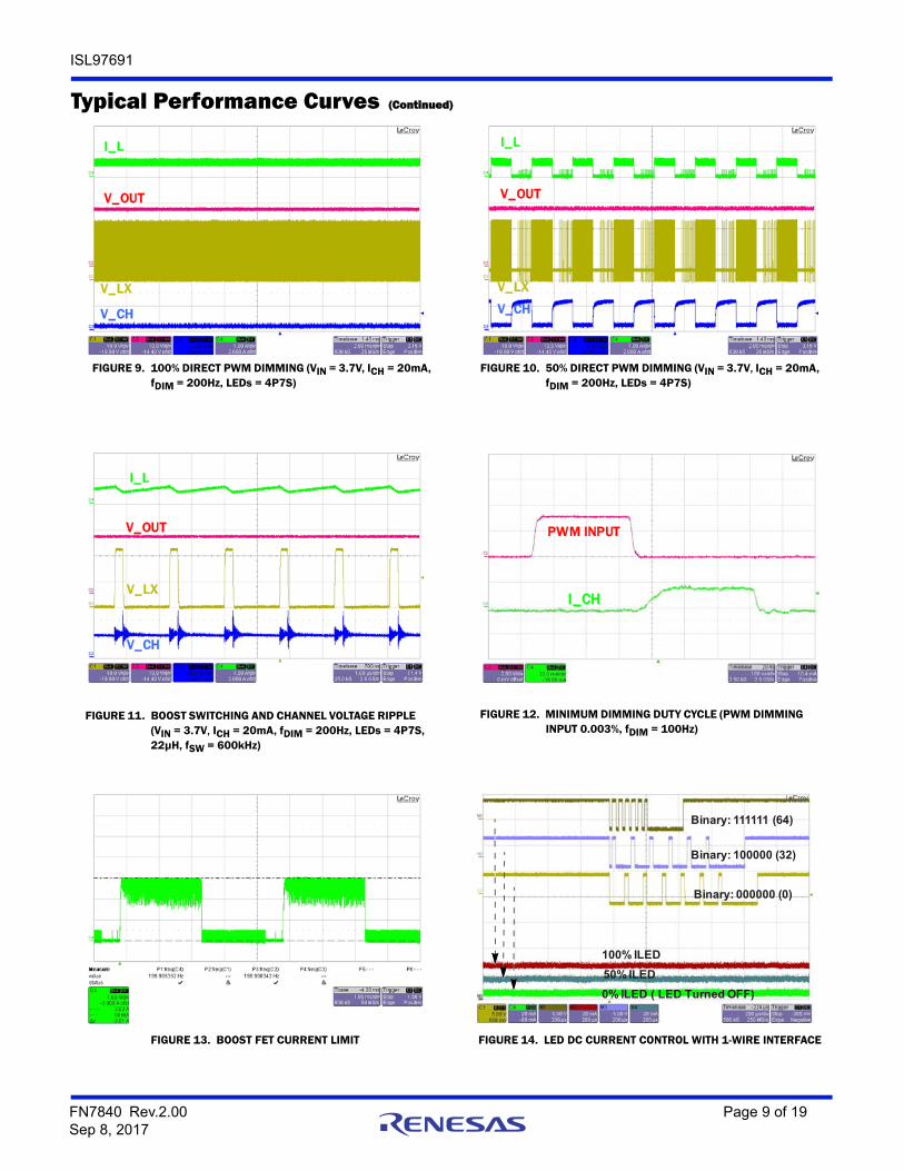
PCB Layout ConsiderationsPCB Layout with TQFN PackageGreat care is needed in designing a PC board for stable ISL97691 operation. As shown in the “Typical Application Circuit” on page 1, the separation of PGND and AGND is essential, keeping the AGND referenced only local to the chip. This minimizes switching noise injection to the feedback sensing and analog areas, as well as eliminating DC errors form high current flow in resistive PC board traces. PGND and AGND should be on the top and bottom layers respectively in the two layer PCB. A star ground connection should be formed by connecting the LED ground return and AGND pins to the thermal pad with vias (Figure 23). The ground connection should be into this ground net, on the top plane. The bottom plane then forms a quiet analog ground area that both shields components on the top plane, as well as providing easy access to all sensitive components. For example, the ground side of the ISET resistor can be dropped to the bottom plane, providing a very low impedance path back to the AGND pin, which does not have any circulating high currents to interfere with it. The bottom plane can also be used as a thermal ground, so the AGND area should be sized sufficiently large to dissipate the required power. For multi-layer boards, the AGND plane can be the second layer. This provides easy access to the AGND net, but allows a larger thermal ground and main ground supply to come up through the thermal vias from a lower plane.
Figure 24 shows the example of the PCB layout of ISL97691. This type of layout is particularly important for this type of product, resulting in high current flow in the main loop’s traces. Careful attention should be focused in the following layout details:
1. Boost input capacitors (CIN), output capacitors (COUT), inductor and Schottky diode should be placed together in a nice tight layout. Keeping the grounds of the input, and output connected with low impedance and wide metal is very important to keep these nodes closely coupled.
2. If possible, try to maintain central ground node on the board and use the input capacitors to avoid excessive input ripple for high output current supplies. The filtering capacitors should be placed close to the VIN pin.
3. For optimum load regulation and true VOUT sensing, the OVP resistors should be connected independently to the top of the output capacitors and away from the higher dv/dt traces. The OVP connection then needs to be as short as possible to the pin. The AGND connection of the lower OVP components is critical for good regulation.
4. The COMP network and the rest of the analog components (on ISET, FSW, etc.) should be referenced to AGND.
5. The heat of the chip is mainly dissipated through the exposed thermal pad so maximizing the copper area around is a good idea. A solid ground is always helpful for the thermal and EMI performance.
6. The inductor and input and output capacitors should be mounted as tight as possible, to reduce the audible noise and inductive ringing.
General Power PAD Design ConsiderationsFigure 23 shows an example of how to use vias to remove heat from the IC. We recommend you fill the thermal pad area with vias. A typical via array would be to fill the thermal pad foot print with vias spaced such that the centre to centre spacing is three times the radius of the via. Keep the vias small, but not so small that their inside diameter prevents solder wicking through the holes during reflow.
FIGURE 23. VIA PATTERN OF ISL97691 TQFN
FN7840 Rev.2.00 Page 15 of 19Sep 8, 2017
ISL97691
Fault Protection and MonitoringThe ISL97691 features extensive protection functions to handle failure conditions automatically. Refer to Figure 15 and Table 3 for details of the fault protections.
The LED failure mode is either open or short circuit. An open circuit failure of an LED only results in the loss of one channel of LEDs without affecting other channels. Similarly, a short circuit condition on a channel that results in that channel being turned off does not affect other channels.
Due to the lag in boost response to any load change at its output, certain transient events (such as LED current steps or significant step changes in LED duty cycle) can transiently look like LED fault modes. The ISL97691 uses feedback from the LEDs to determine when it is in a stable operating region and prevents apparent faults during these transient events from allowing any of the LED stacks to fault out. See Table 3 for more details.
Short Circuit Protection (SCP) The short circuit detection circuit monitors the voltage on each channel and disables faulty channels which are above the short circuit protection threshold, nominally 8V (the action taken is described in Table 3).
Open Circuit Protection (OCP)When one of the LEDs becomes open circuit, it can behave as either an infinite resistance or a gradually increasing finite resistance. The ISL97691 monitors the current in each channel such that any string which reaches the intended output current is considered “good”. Should the current subsequently fall below the target, the channel will be considered an “open circuit”. Furthermore, should the boost output of the ISL97691 reach the VOVP limit, all channels which are not “good” will immediately be considered as “open circuit”.
Detection of an “open circuit” channel will result in a time-out before disabling of the affected channel.
Undervoltage LockoutIf the input voltage falls below the VUVLO level of ~2.15V, the ISL97691 will stop switching and be reset. Operation will restart only if the VIN is back in the normal operating range.
Over-Temperature Protection (OTP)The ISL97691 has an over-temperature protection threshold set to +150°C. If this threshold is reached, the boost stops switching and the channel output current sinks are switched off. The ISL97691 can be restarted by toggling VIN to below the VUVLO level of ~2.15V, then back up to the normal input voltage level.
FIGURE 24. EXAMPLE OF PCB LAYOUT
FN7840 Rev.2.00 Page 16 of 19Sep 8, 2017

ISL97691
FIGURE 25. SIMPLIFIED FAULT PROTECTIONS
Qx
CHx
DC1
PWM/OC1/SC1
REF
FETDRIVER
LX
IMAX ILIMIT
OVP
VIN
T2
OTP
THRMSHDN
Q1
VSC CH1
VOUT
DC2
PWM/OCx/SCx
TEMPSENSOR
LOGIC
T1
OTP
THRMSHDN
O/PSHORT
FAULTDETECTLOGIC
PWMGENERATOR
FAULT FLAG
TABLE 3. PROTECTIONS TABLE
CASE FAILURE MODE DETECTION MODE FAILED CHANNEL ACTION GOOD CHANNELS ACTIONVOUT
REGULATED BY
1 CH1 Short Circuit Over-Temperature Protection (OTP) not triggered, CH1 < 8V
CH1 ON and burns power CH2 through CH4 Normal Highest LED string VF of CH2 - CH4
2 CH1 Short Circuit OTP triggered Boost converter and channels are shut down until VIN is cycled -
3 CH1 Short Circuit OTP not triggered, CH1 > 8V CH1 disabled after 190ms time-out
CH2 through CH4 Normal Highest LED string VF of CH2 - CH4
4 CH1 Open Circuit withinfinite resistance
OTP not triggered, CH1 < 8V VOUT will ramp to OVP. CH1 will time-out after 190ms and switch off. VOUT will then reduce to normal level
CH2 through CH4 Normal Highest LED string VF of CH2 - CH4
5 Output LED stack voltage too high
VOUT = VOVP Any channel that is below the target current will time-out after 190ms while VOUT is regulated at VOVP, and VOUT will then return to the normal regulation voltage required for other channels
Highest LED stringVF of CH1 - CH4
FN7840 Rev.2.00 Page 17 of 19Sep 8, 2017

ISL97691
Intersil products are manufactured, assembled and tested utilizing ISO9001 quality systems as notedin the quality certifications found at www.intersil.com/en/support/qualandreliability.html
Intersil products are sold by description only. Intersil may modify the circuit design and/or specifications of products at any time without notice, provided that such modification does not, in Intersil's sole judgment, affect the form, fit or function of the product. Accordingly, the reader is cautioned to verify that datasheets are current before placing orders. Information furnished by Intersil is believed to be accurate and reliable. However, no responsibility is assumed by Intersil or its subsidiaries for its use; nor for any infringements of patents or other rights of third parties which may result from its use. No license is granted by implication or otherwise under any patent or patent rights of Intersil or its subsidiaries.
For information regarding Intersil Corporation and its products, see www.intersil.com
For additional products, see www.intersil.com/en/products.html
© Copyright Intersil Americas LLC 2012-2017. All Rights Reserved.All trademarks and registered trademarks are the property of their respective owners.
About IntersilIntersil Corporation is a leading provider of innovative power management and precision analog solutions. The company's products address some of the largest markets within the industrial and infrastructure, mobile computing, and high-end consumer markets.
For the most updated datasheet, application notes, related documentation, and related parts, see the respective product information page found at www.intersil.com.
For a listing of definitions and abbreviations of common terms used in our documents, visit www.intersil.com/glossary.
You can report errors or suggestions for improving this datasheet by visiting www.intersil.com/ask.
Reliability reports are also available from our website at www.intersil.com/support.
Revision HistoryThe revision history provided is for informational purposes only and is believed to be accurate, but not warranted. Please visit our website to make sure you have the latest revision.
DATE REVISION CHANGE
September 8, 2017 FN7840.2 Applied new header/footer.Added Related Literature on page 1.Updated Ordering Information notes.Added VHEADROOM_RANGE spec to Electrical Specifications table. Added corresponding Note 11.In the Current Matching and Current Accuracy section - updated 2nd sentence in paragraph 2 for clarification.Updated About Intersil section.
November 26, 2012 FN7840.1 Updated Features on page 1.Removed EN from PWM_2 pin in Typical Application Circuit on page 1 and from the PWMI_2 in Block Diagram on page 2.Added “Operation with Input Voltage Greater than 5.5V” on page 12.Added Figure “LED DRIVER OPERATION WITH INPUT VOLTAGE UP TO 26V” on page 13.
In “Absolute Maximum Ratings” on page 5, changed HBM from 2kV to 2.5kV. Changed CDM from 1kV to 2kV.
June 13, 2012 FN7840.0 Initial release.
FN7840 Rev.2.00 Page 18 of 19Sep 8, 2017

ISL97691
FN7840 Rev.2.00 Page 19 of 19Sep 8, 2017
Package Outline Drawing
L16.3x3D16 LEAD THIN QUAD FLAT NO-LEAD PLASTIC PACKAGERev 0, 3/10
located within the zone indicated. The pin #1 identifier may be
Unless otherwise specified, tolerance : Decimal ± 0.05
Tiebar shown (if present) is a non-functional feature.
The configuration of the pin #1 identifier is optional, but must be
between 0.15mm and 0.25mm from the terminal tip.
Dimension applies to the metallized terminal and is measured
Dimensions in ( ) for Reference Only.
Dimensioning and tolerancing conform to ASME Y14.5m-1994.
6.
either a mold or mark feature.
3.
5.
4.
2.
Dimensions are in millimeters.1.
NOTES:
BOTTOM VIEW
DETAIL "X"
SIDE VIEW
TYPICAL RECOMMENDED LAND PATTERN
TOP VIEW
(4X) 0.15
INDEX AREAPIN 1
A3.00
B
3.0
0
PIN #1
B0.10 M AC
4
6
6
±0.05
112
49
13 16
8 5
1.60 SQ
16X 0.23
16X 0.40±0.10
4X 1.50
12X 0.50
(16X 0.60)
( 1.60)(2.80 TYP)
(16X 0.23)
(12X 0.50)
C 0 . 2 REF
0 . 05 MAX.0 . 02 NOM.
5
0.75 ±0.05
0.08
0.10C
C
C
INDEX AREA
SEE DETAIL “X”
JEDEC reference drawing: MO-220 WEED.7.
For the most recent package outline drawing, see L16,3x3D.