Embed Size (px)
Citation preview
General DescriptionThe MAX3850 is a +3.3V DC-coupled laser driver forSDH/SONET applications up to 2.7Gbps. The deviceaccepts differential data and clock inputs and providesbias and modulation currents for driving a laser. If aclock signal is available, a synchronizing input latchcan be used to reduce jitter. An automatic power-con-trol (APC) feedback loop is incorporated to maintain aconstant average optical power over temperature andlifetime. The wide modulation current range of 5mA to60mA (up to 80mA AC-coupled) and bias current of1mA to 100mA are easy to program, making this prod-uct ideal for SDH/SONET applications. The MAX3850also provides laser current-enable control, two currentmonitors that are directly proportional to the laser biasand modulation currents, and a failure-monitor output toindicate when the APC loop is unable to maintain theaverage optical power. Designed to be DC-coupled tothe laser with a supply voltage of only 3.3V, theMAX3850 greatly simplifies interface requirements. TheMAX3850 is available in a small 32-pin QFN packageas well as dice.
Applications
Features♦ Single +3.3V Power Supply
♦ 35mA Supply Current
♦ Programmable Bias Current from 1mA to 100mA
♦ Programmable Modulation Current from 5mA to60mA (Up to 80mA AC-Coupled)
♦ Bias Current and Modulation Current Monitors
♦ 70ps Rise/Fall Time
♦ Automatic Average Power Control with FailureMonitor
♦ Complies with ANSI, ITU, and BellcoreSDH/SONET Specifications
♦ Laser Current-Enable Control
MA
X3
85
0
2.7Gbps, +3.3V DC-Coupled Laser Driver
________________________________________________________________ Maxim Integrated Products 1
SERIALIZERWITH
CLOCK GEN
11Ω
LD
16Ω
50Ω
8.0pF
3.3V3.3V0.01μF
BIASMONMODMON
3.3V
1000pF
BIAS
MAX
LATC
H
ENAB
LE
FAIL
MOD
SET
APCS
ET
APCF
ILT
GND
CLOCK-
CLOCK+
DATA-
DATA+
OUT+
BIASMD
OUT-
CAPC
MAX3850
MAX3890
100Ω
100Ω
TYPICAL APPLICATION CIRCUITWITH DC-COUPLED INPUTS
392Ω 392Ω
VCC
0.1μF 0.1μF
Ordering Information
Typical Application Circuits
19-2294; Rev 1; 5/03
For pricing, delivery, and ordering information, please contact Maxim/Dallas Direct! at 1-888-629-4642, or visit Maxim’s website at www.maxim-ic.com.
*Dice are designed to operate over this range, but are testedand guaranteed at TA = +25°C only. Contact factory for availability.Typical Application Circuits are continued at the end of thedata sheet.
Pin Configuration appears at the end of the data sheet.
PARTTEMP
RANGEPIN-PACKAGE
PACKAGECODE
MAX3850EGJ - 40°C to + 85°C 32 QFN G3255-1
MAX3850E/D - 40°C to + 85°C Dice* —
SDH/SONET TransmissionSystems
MPLS Transmitter Systems
Add/Drop MultiplexersDigital Cross-ConnectsSection Regenerators
EVALUATION KIT
AVAILABLE

MA
X3
85
0
2.7Gbps, +3.3V DC-Coupled Laser Driver
2 _______________________________________________________________________________________
ABSOLUTE MAXIMUM RATINGS
DC ELECTRICAL CHARACTERISTICS(VCC = +3.0V to +3.6V, TA = -40°C to +85°C. Typical values are at VCC = +3.3V, IMOD = 30mA, IBIAS = 60mA, TA = +25°C, unless otherwise noted.) (Note 1)
Stresses beyond those listed under “Absolute Maximum Ratings” may cause permanent damage to the device. These are stress ratings only, and functionaloperation of the device at these or any other conditions beyond those indicated in the operational sections of the specifications is not implied. Exposure toabsolute maximum rating conditions for extended periods may affect device reliability.
Supply Voltage, VCC..............................................-0.5V to +4.0VCurrent into BIAS ............................................-20mA to +150mACurrent into OUT+, OUT- ................................-20mA to +100mACurrent into MD.....................................................-5mA to +5mAVoltage at DATA+, DATA-, CLK+, CLK-, ENABLE, LATCH,
FAIL, BIASMON, MODMON, CAPC,MODSET, BIASMAX, APCSET................-0.5V to (VCC + 0.5V)
Voltage at APCFILT ...............................................-0.5V to +3.0VVoltage at OUT+, OUT-.............................................0.4V to 4.8V
Voltage at BIAS............................................1.0V to (VCC + 0.5V)Continuous Power Dissipation (TA = +85°C)
32-Pin QFN (derate 21.2mW/°C above +85°C) ........13.84mWStorage Temperature Range .............................-65°C to +165°COperating Junction Temperature Range...........-55°C to +150°CProcessing Temperature (die) .........................................+400°CLead Temperature (soldering,10s) ..................................+300°C
PARAMETER SYMBOL CONDITIONS MIN TYP MAX UNITS
Supply Voltage VCC 3.0 3.3 3.6 V
Supply Current ICC (Note 2) 35 65 mA
Bias-Current Range IBIAS (Note 3) 1 100 mA
Bias Off-Current IBIAS-OFF ENABLE = low (Note 4) 100 µA
IBIAS = 100mA -480 12 480Bias-Current Stability APC open loop
IBIAS = 1mA -1000 456 1000ppm/°C
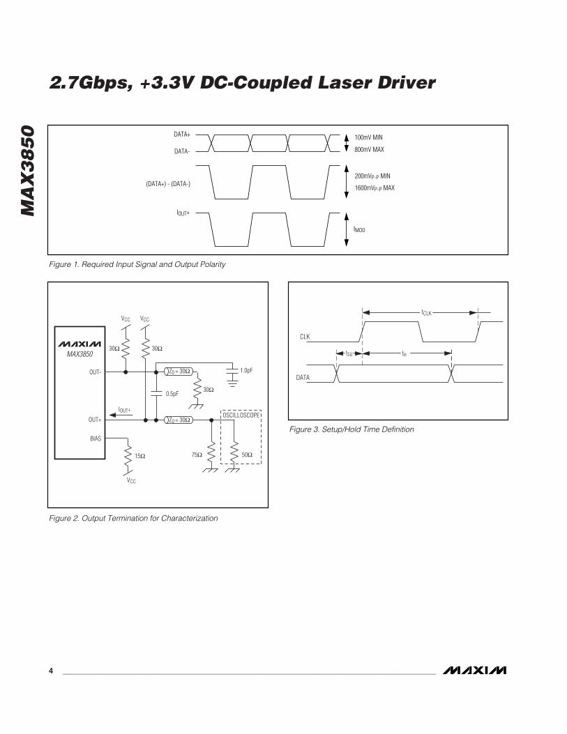
Differential Input Voltage Range VID (Figure 1) 200 1600 mVP-P
Common-Mode Input Voltage VICM LVPECL compatibleVCC -1.49
VCC -1.32
VCC -VID/4
V
TTL Input High Voltage ENABLE, LATCH 2.0 V
TTL Input Low Voltage ENABLE, LATCH 0.8 V
TTL Output High Voltage FAIL sourcing 50µA 2.4VCC -0.3
VCC V
TTL Output Low Voltage Sinking 100µA 0 0.025 0.4 V
Monitor-Diode Reverse BiasVoltage
1.5 V
Monitor-Diode DC Current Range IMD 18 1000 µA
IMD = 1mA -480 95 480Monitor-Diode Set-Point Stability (Note 6)
IMD = 18µA -1000 295 1000ppm/°C
Monitor-Diode Bias AbsoluteAccuracy
(Note 5) -15 +15 %
BIASMON to IBIAS Gain ABIAS IBIAS/IBIASMON 36 41 46 A/A
MODMON to IMOD Gain AMOD IMOD/IMODMON 25 30 35 A/A
VOUT+, VOUT- = 0.6V (DC-coupled) 5 60Modulation-Current Range IMOD
VOUT+, VOUT- = 2.0V (AC-coupled) 5 80mA
MA
X3
85
0
2.7Gbps, +3.3V DC-Coupled Laser Driver
_______________________________________________________________________________________ 3
DC ELECTRICAL CHARACTERISTICS (continued)(VCC = +3.0V to +3.6V, TA = -40°C to +85°C. Typical values are at VCC = +3.3V, IMOD = 30mA, IBIAS = 60mA, TA = +25°C, unless otherwise noted.) (Note 1)
AC ELECTRICAL CHARACTERISTICS(VCC = +3.0V to +3.6V, IMOD = 5mA to 60mA, TA = -40°C to +85°C. Typical values are at VCC = +3.3V, IMOD = 30mA, TA = +25°C.)(Note 7)
Note 1: Dice are tested at TA = +25°C only. Specifications at -40°C are guaranteed by design and characterization.Note 2: Tested at RMODSET = 2.61kΩ, RBIASMAX = 1.96kΩ, excluding IBIAS and IMOD.Note 3: Voltage on BIAS pin is (VCC - 1.5V).Note 4: The bias and modulation currents will be switched off if any of the current set pins are grounded.Note 5: Accuracy refers to part-to-part variation.Note 6: Assuming the laser-to-monitor diode transfer function does not change with temperature. Guaranteed by design and
characterization.Note 7: AC characteristics are guaranteed by design and characterization using the characterization circuit of Figure 2.Note 8: Measured with repeating 0000 1111 pattern, LATCH = high.
PARAMETER SYMBOL CONDITIONS MIN TYP MAX UNITS
Modulation Off-Current IMOD-OFF ENABLE = low (Note 4) 100 µA
IMOD = 60mA -480 66 480Modulation-Current Stability
IMOD = 5mA -1000 110 1000ppm/°C
PARAMETER SYMBOL CONDITIONS MIN TYP MAX UNITS
Maximum Data Rate 2.7 Gbps
Input Latch Setup Time tSU LATCH = high (Figure 3) 90 ps
Input Latch Hold Time tH LATCH = high (Figure 3) 60 ps
Output Rise Time tR 20% to 80% ed g e sp eed s ( N ote 8) 66 110 ps
Output Fall Time tF 20% to 80% ed g e sp eed s ( N ote 8) 70 100 ps
30mA ≤ IMOD ≤ 60 (Note 8) ±2Output Overshoot
IMOD = 5mA (Note 8) ±12%
IMOD Enable/Startup Delay 270 ns
IBIAS Typical Startup Delay APC open loop, CAPC and CAPCFILT = 0 370 ns
Output Random Jitter RJOUT (Note 8) 0.66 1.4 psRMS
Output Deterministic Jitter TJOUTLATCH = high, 27- 1 PRBS with 80 inserted 0sand 80 inserted 1s
8.6 50 psP-P
MA
X3
85
0
2.7Gbps, +3.3V DC-Coupled Laser Driver
4 _______________________________________________________________________________________
DATA+
DATA-
(DATA+) - (DATA-)
IOUT+
100mV MIN
800mV MAX
200mVP-P MIN
1600mVP-P MAX
IMOD
Figure 1. Required Input Signal and Output Polarity
CLK
DATA
tCLK
tSU tH
Figure 3. Setup/Hold Time Definition
30Ω30Ω
OUT+
BIAS
OUT-
15Ω
OSCILLOSCOPE
50Ω75Ω
30Ω0.5pF
1.0pF
Z0 = 30Ω
Z0 = 30Ω
VCC
VCC VCC
MAX3850
IOUT+
Figure 2. Output Termination for Characterization
MA
X3
85
0
2.7Gbps, +3.3V DC-Coupled Laser Driver
_______________________________________________________________________________________ 5
OPTICAL EYE DIAGRAM(2.7Gbps, 130mm FP LASER1.87Gbps FILTER, 32-QFN)
MAX3850 toc01
MITSUBISHI ML725C8F LASER DIODE
BIAS CURRENT ENABLESTARTUP DELAY vs. CAPC
MAX
3850
toc0
2
CAPC (F)
STAR
TUP
DELA
Y (m
s)
0.1µ0.01µ1000p
1.0
10
100
0.1100p 1.0µ
ELECTRICAL EYE DIAGRAM(IMOD = 25mA, 213 - 1 + 80 CID, 32 QFN)
MAX
3850
toc0
3
58ps/div
ELECTRICAL EYE DIAGRAM(IMOD = 60mA, 213 - 1 + 80 CID, 32 QFN)
MAX
3850
toc0
4
58ps/div
ELECTRICAL EYE DIAGRAMAC-COUPLED
(IMOD = 80mA, 213 - 1 + 80 CID, 32 QFN)M
AX38
50 to
c05
58ps/div
RANDOM JITTER vs. IMOD
MAX
3850
toc0
6IMOD (mA)
RAND
OM JI
TTER
(psm
s)
50403020
0.2
0.4
0.6
0.8
1.0
1.2
1.4
1.6
1.8
2.0
010 60
DETERMINISTIC JITTER vs. IMOD
MAX
3850
toc0
7
IMOD (mA)
TOTA
L JIT
TER
(ps P
-P)
50403020
5
10
15
20
25
30
010 60
IBIASMAX vs. RBIASMAX
MAX
3850
toc0
8
RBIASMAX (Ω)
I BIA
SMAX
(mA)
10k
1501401301201101009080706050403020100
1k 100k
IMOD vs. RMODSET
MAX
3850
toc0
9
RMODSET (Ω)
I MOD
(mA)
10k
10
20
30
40
50
60
70
01k 100k
Typical Operating Characteristics(DC-coupled output, TA = +25°C, unless otherwise noted.)
MA
X3
85
0
2.7Gbps, +3.3V DC-Coupled Laser Driver
6 _______________________________________________________________________________________
Typical Operating Characteristics (continued)(DC-coupled output, TA = +25°C, unless otherwise noted.)
IMD vs. RAPCSETM
AX38
50 to
c10
RAPCSET (Ω)
I MD
(mA)
10k1k
0.2
0.4
0.6
0.8
1.0
1.2
1.4
1.6
0100 100k
SUPPLY CURRENT vs. TEMPERATURE(EXCLUDES IBIAS, IMOD, 15Ω LOAD)
MAX
3850
toc1
1
TEMPERATURE (°C)
SUPP
LY C
URRE
NT (m
A)
603510-15
20
30
40
50
60
70
10-40 85
VCC = 3.0V VCC = 3.3V VCC = 3.6V
BIAS-CURRENT MONITOR GAINvs. TEMPERATURE
MAX
3850
toc1
2
TEMPERATURE (°C)
GAIN
(IBI
AS /I
BIAS
MON
)
603510-15
20
25
30
35
40
45
50
15-40 85
IBIAS = 100mA, IMOD = 50mA
IBIAS = 10mA, IMOD = 10mA
MODULATION-CURRENT MONITOR GAINvs. TEMPERATURE
MAX
3850
toc1
3
TEMPERATURE (°C)
GAIN
(IM
OD/I M
ODM
ON)
603510-15
5
10
15
20
25
30
35
0-40 85
IBIAS = 100mA, IMOD = 50mA
IBIAS = 10mA, IMOD = 10mA
PULSE-WIDTH DISTORTION vs. IMOD
MAX
3850
toc1
4
IMOD (mA)
PWD
(ps)
50403020
2
4
6
8
10
12
14
16
18
010 60
VCC = 3.0V
MA
X3
85
0
2.7Gbps, +3.3V DC-Coupled Laser Driver
_______________________________________________________________________________________ 7
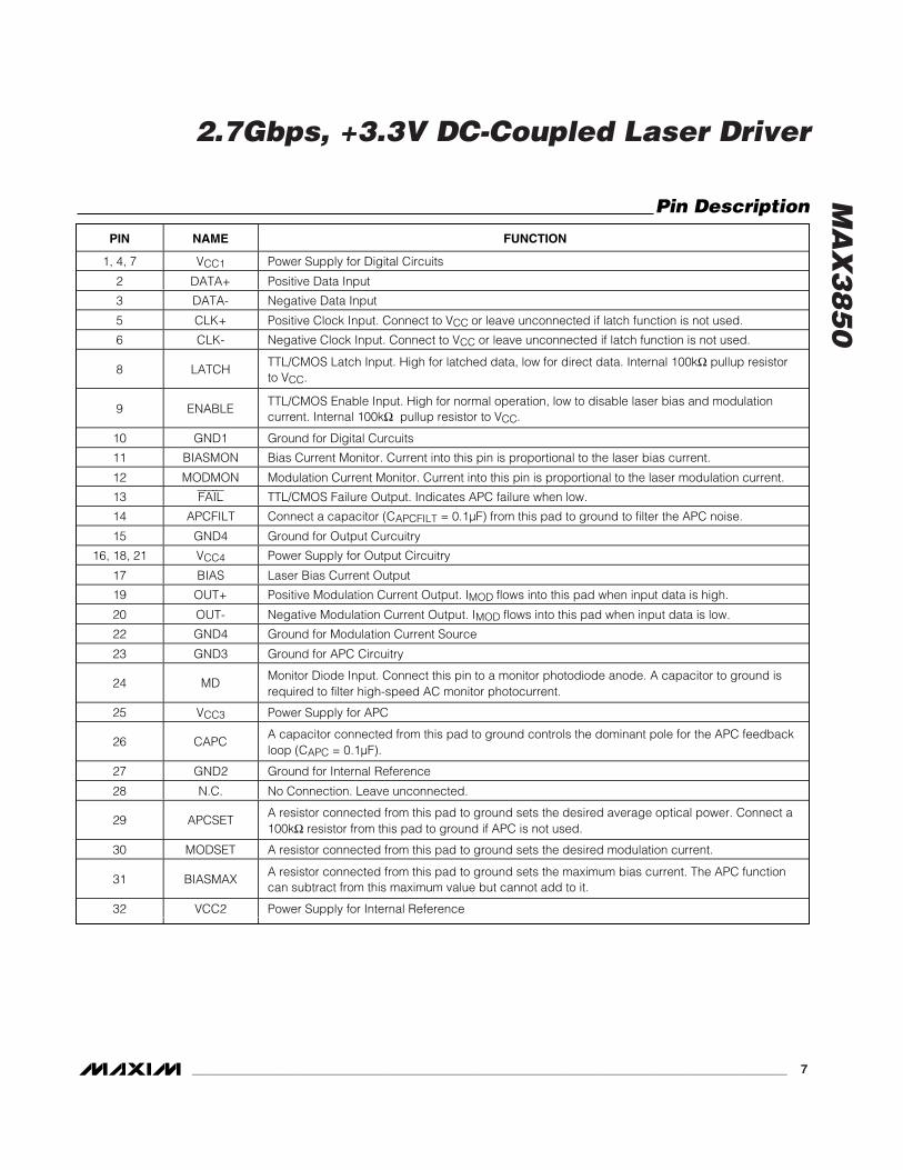
Pin Description
PIN NAME FUNCTION
1, 4, 7 VCC1 Power Supply for Digital Circuits
2 DATA+ Positive Data Input
3 DATA- Negative Data Input
5 CLK+ Positive Clock Input. Connect to VCC or leave unconnected if latch function is not used.
6 CLK- Negative Clock Input. Connect to VCC or leave unconnected if latch function is not used.
8 LATCHTTL/CMOS Latch Input. High for latched data, low for direct data. Internal 100kΩ pullup resistorto VCC.
9 ENABLETTL/CMOS Enable Input. High for normal operation, low to disable laser bias and modulationcurrent. Internal 100kΩ pullup resistor to VCC.
10 GND1 Ground for Digital Curcuits
11 BIASMON Bias Current Monitor. Current into this pin is proportional to the laser bias current.
12 MODMON Modulation Current Monitor. Current into this pin is proportional to the laser modulation current.
13 FAIL TTL/CMOS Failure Output. Indicates APC failure when low.
14 APCFILT Connect a capacitor (CAPCFILT = 0.1µF) from this pad to ground to filter the APC noise.
15 GND4 Ground for Output Curcuitry
16, 18, 21 VCC4 Power Supply for Output Circuitry
17 BIAS Laser Bias Current Output
19 OUT+ Positive Modulation Current Output. IMOD flows into this pad when input data is high.
20 OUT- Negative Modulation Current Output. IMOD flows into this pad when input data is low.
22 GND4 Ground for Modulation Current Source
23 GND3 Ground for APC Circuitry
24 MDMonitor Diode Input. Connect this pin to a monitor photodiode anode. A capacitor to ground isrequired to filter high-speed AC monitor photocurrent.
25 VCC3 Power Supply for APC
26 CAPCA capacitor connected from this pad to ground controls the dominant pole for the APC feedbackloop (CAPC = 0.1µF).
27 GND2 Ground for Internal Reference
28 N.C. No Connection. Leave unconnected.
29 APCSETA resistor connected from this pad to ground sets the desired average optical power. Connect a100kΩ resistor from this pad to ground if APC is not used.
30 MODSET A resistor connected from this pad to ground sets the desired modulation current.
31 BIASMAXA resistor connected from this pad to ground sets the maximum bias current. The APC functioncan subtract from this maximum value but cannot add to it.
32 VCC2 Power Supply for Internal Reference
MA
X3
85
0
2.7Gbps, +3.3V DC-Coupled Laser Driver
8 _______________________________________________________________________________________
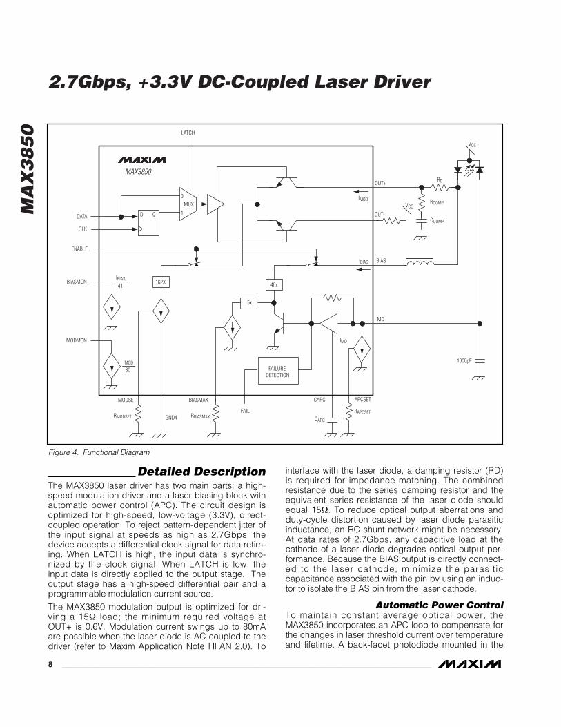
Detailed DescriptionThe MAX3850 laser driver has two main parts: a high-speed modulation driver and a laser-biasing block withautomatic power control (APC). The circuit design isoptimized for high-speed, low-voltage (3.3V), direct-coupled operation. To reject pattern-dependent jitter ofthe input signal at speeds as high as 2.7Gbps, thedevice accepts a differential clock signal for data retim-ing. When LATCH is high, the input data is synchro-nized by the clock signal. When LATCH is low, theinput data is directly applied to the output stage. Theoutput stage has a high-speed differential pair and aprogrammable modulation current source.
The MAX3850 modulation output is optimized for dri-ving a 15Ω load; the minimum required voltage atOUT+ is 0.6V. Modulation current swings up to 80mAare possible when the laser diode is AC-coupled to thedriver (refer to Maxim Application Note HFAN 2.0). To
interface with the laser diode, a damping resistor (RD)is required for impedance matching. The combinedresistance due to the series damping resistor and theequivalent series resistance of the laser diode shouldequal 15Ω. To reduce optical output aberrations andduty-cycle distortion caused by laser diode parasiticinductance, an RC shunt network might be necessary.At data rates of 2.7Gbps, any capacitive load at thecathode of a laser diode degrades optical output per-formance. Because the BIAS output is directly connect-ed to the laser cathode, minimize the parasit iccapacitance associated with the pin by using an induc-tor to isolate the BIAS pin from the laser cathode.
Automatic Power ControlTo maintain constant average optical power, theMAX3850 incorporates an APC loop to compensate forthe changes in laser threshold current over temperatureand lifetime. A back-facet photodiode mounted in the
Figure 4. Functional Diagram
D Q
0
1MUX
162X
FAILUREDETECTION
40x
5x
OUT-
OUT+
IMOD
MAX3850
IBIAS
41
IMOD
30
MODMON
BIASMON
ENABLE
CLK
DATA
LATCH
IBIAS
IMD
MODSET
RMODSET
BIASMAX
RBIASMAXFAIL
CAPC
RAPCSET
APCSET
CAPC
MD
BIAS
VCCRCOMP
CCOMP
RD
VCC
1000pF
GND4
MA
X3
85
0
2.7Gbps, +3.3V DC-Coupled Laser Driver
_______________________________________________________________________________________ 9
laser package converts the optical power into a pho-tocurrent. The APC loop adjusts the laser bias currentso that the monitor current is matched to a referencecurrent set by RAPCSET. The time constant of the APCloop is determined by an external capacitor (CAPC). Toeliminate the pattern-dependent jitter associated withthe APC loop time constant, and to guarantee loop sta-bility, the recommended value for CAPC is 0.1µF.
When the APC loop is functioning, an external resistor(RBIASMAX) sets the maximum allowable bias current.An APC failure flag (FAIL) is set low when the bias cur-rent cannot be adjusted to achieve the desired averageoptical power. To filter APC loop noise, use an externalcapacitor at APCFILT with a recommended value of 0.1µF.
APC closed-loop operation requires that the user setthree currents with external resistors connected betweenground and BIASMAX, MODSET, and APCSET. Detailedguidelines for these resistor settings are described in theDesign Procedure section.
Open-Loop OperationIf necessary, the MAX3850 is fully operational withoutAPC. To operate the MAX3850 open loop, connect a100kΩ resistor from RAPCSET to GND and leave MDunconnected. In this case, the laser current is directlyset by two external resistors connected from ground toBIASMAX and MODSET.
Optional Data Input LatchIf LATCH is high, the input data is retimed by the risingedge of CLK+. If LATCH is low, the input data is direct-ly connected to the output stage. When not using theLATCH function, connect CLK+ and CLK- to VCC orleave unconnected.
Enable ControlThe MAX3850 incorporates a laser-driver enable func-tion. When ENABLE is low, the bias and modulationcurrents are off. For open-loop operation, the typicalenable time is 370ns, and the typical disable time is20ns. For closed-loop operation, the bias current iscontrolled by the APC loop, and the enable time will beaffected by the APC loop time constant. With CAPC =0.1µF, typical closed-loop enable time is 10ms, andtypical closed-loop disable time is 40ns. For more infor-mation, see the Bias Current Enable Time TypicalOperating Characteristics.
Current MonitorsThe MAX3850 features bias and modulation-currentmonitor outputs. The BIASMON output sinks a currentequal to 1/41 of the laser bias current, IBIAS/41. TheMODMON output sinks a current equal to 1/30 of the
laser modulation current, IMOD/30. BIASMON andMODMON should be connected through a pullup resis-tor to VCC. Choose a pullup resistor value that ensuresa voltage at BIASMON greater than VCC - 1.5V and avoltage at MODMON greater than VCC - 2.0V. Thesepins should be connected VCC if not used.
Slow-StartFor laser safety reasons, the MAX3850 incorporates aslow-start circuit that provides a delay of 370ns forenabling a laser diode.
APC Failure MonitorThe MAX3850 provides an APC failure monitor(TTL/CMOS) to indicate an APC loop-tracking failure.FAIL is set low when the APC cannot adjust the biascurrent to maintain the desired monitor current. Forexample, the laser diode requires more bias current (tomaintain a constant optical output) than maximum biascurrent set by RBIASMAX. The bias current is limited andFAIL will be asserted. In an alternate example, assumethat a circuit failure causes the cathode of the laserdiode to be shorted to GND, thereby causing an uncon-trolled high optical output. In this case, the APC loopcannot decrease the user current, and FAIL will beasserted.
Short-Circuit ProtectionThe MAX3850 provides short-circuit protection forthe modulation, bias, and monitor current sources. IfBIASMAX, MODSET, or APCSET is shorted to ground,bias and modulation output will be turned off.
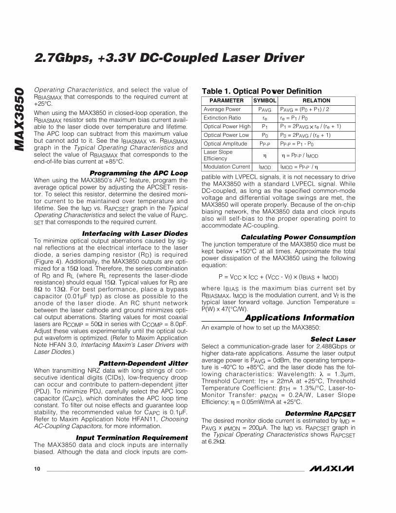
Design ProcedureWhen designing a laser transmitter, the optical outputusually is expressed in terms of average power andextinction ratio. Table 1 shows the relationships helpfulin converting between the optical average power andthe modulation current. These relationships are valid ifthe mark density and duty cycle of the optical waveformare 50%.
Programming the Modulation CurrentFor a given laser power (PAVG), slope efficiency (η),and extinction ratio (re), the modulation current can becalculated using Table 1. See the IMOD vs. RMODSETgraph in the Typical Operating Characteristics, andselect the value of RMODSET that corresponds to therequired current at +25°C.
Programming the Bias CurrentWhen the MAX3850 is used in open-loop operation, theRBIASMAX resistor determines the bias current. To selectthis resistor, determine the required bias current at +25°C.See the IBIASMAX vs. RBIASMAX graph in the Typical
MA
X3
85
0
2.7Gbps, +3.3V DC-Coupled Laser Driver
10 ______________________________________________________________________________________
Operating Characteristics, and select the value of RBIASMAX that corresponds to the required current at+25°C.
When using the MAX3850 in closed-loop operation, theRBIASMAX resistor sets the maximum bias current avail-able to the laser diode over temperature and lifetime.The APC loop can subtract from this maximum valuebut cannot add to it. See the IBIASMAX vs. RBIASMAXgraph in the Typical Operating Characteristics andselect the value of RBIASMAX that corresponds to theend-of-life bias current at +85°C.
Programming the APC LoopWhen using the MAX3850’s APC feature, program theaverage optical power by adjusting the APCSET resis-tor. To select this resistor, determine the desired moni-tor current to be maintained over temperature andlifetime. See the IMD vs. RAPCSET graph in the TypicalOperating Characteristics and select the value of RAPC-SET that corresponds to the required current.
Interfacing with Laser DiodesTo minimize optical output aberrations caused by sig-nal reflections at the electrical interface to the laserdiode, a series damping resistor (RD) is required(Figure 4). Additionally, the MAX3850 outputs are opti-mized for a 15Ω load. Therefore, the series combinationof RD and RL (where RL represents the laser-dioderesistance) should equal 15Ω. Typical values for RD are8Ω to 13Ω. For best performance, place a bypasscapacitor (0.01µF typ) as close as possible to theanode of the laser diode. An RC shunt networkbetween the laser cathode and ground minimizes opti-cal output aberrations. Starting values for most coaxiallasers are RCOMP = 50Ω in series with CCOMP = 8.0pF.Adjust these values experimentally until the optical out-put waveform is optimized. (Refer to Maxim ApplicationNote HFAN 3.0, Interfacing Maxim’s Laser Drivers withLaser Diodes.)
Pattern-Dependent JitterWhen transmitting NRZ data with long strings of con-secutive identical digits (CIDs), low-frequency droopcan occur and contribute to pattern-dependent jitter(PDJ). To minimize PDJ, carefully select the APC loopcapacitor (CAPC), which dominates the APC loop timeconstant. To filter out noise effects and guarantee loopstability, the recommended value for CAPC is 0.1µF.Refer to Maxim Application Note HFAN11, ChoosingAC-Coupling Capacitors, for more information.
Input Termination RequirementThe MAX3850 data and clock inputs are internallybiased. Although the data and clock inputs are com-
patible with LVPECL signals, it is not necessary to drivethe MAX3850 with a standard LVPECL signal. WhileDC-coupled, as long as the specified common-modevoltage and differential voltage swings are met, theMAX3850 will operate properly. Because of the on-chipbiasing network, the MAX3850 data and clock inputsalso will self-bias to the proper operating point toaccommodate AC-coupling.
Calculating Power ConsumptionThe junction temperature of the MAX3850 dice must bekept below +150°C at all times. Approximate the totalpower dissipation of the MAX3850 using the followingequation:
P = VCC ICC + (VCC - Vf) (IBIAS + IMOD)
where IBIAS is the maximum bias current set by RBIASMAX, IMOD is the modulation current, and Vf is thetypical laser forward voltage. Junction Temperature =P(W) x 47(°C/W).
Applications InformationAn example of how to set up the MAX3850:
Select LaserSelect a communication-grade laser for 2.488Gbps orhigher data-rate applications. Assume the laser outputaverage power is PAVG = 0dBm, the operating tempera-ture is -40°C to +85°C, and the laser diode has the fol-lowing characteristics: Wavelength: λ = 1.3µm,Threshold Current: ITH = 22mA at +25°C, ThresholdTemperature Coefficient: βTH = 1.3%/°C, Laser-to-Monitor Transfer: ρMON = 0.2A/W, Laser SlopeEfficiency: η = 0.05mW/mA at +25°C.
Determine RAPCSETThe desired monitor diode current is estimated by IMD =PAVG x ρMON = 200µA. The IMD vs. RAPCSET graph inthe Typical Operating Characteristics shows RAPCSETat 6.2kΩ.
Table 1. Optical Power DefinitionRELATION
PAVG = (P0 + P1) / 2
re = P1 / P0
P1 = 2PAVG re / (re + 1)
P0 = 2PAVG / (re + 1)
PP-P = P1 - P0
η = PP-P / IMOD
IMOD = PP-P / ηIMOD
η
PP-P
P0
P1
re
PAVG
SYMBOLPARAMETER
Average Power
Extinction Ratio
Optical Power High
Optical Power Low
Optical Amplitude
Laser SlopeEfficiency
Modulation Current
MA
X3
85
0
2.7Gbps, +3.3V DC-Coupled Laser Driver
______________________________________________________________________________________ 11
Determine RMODSETAssuming re = 20, and average power of 0dBm (1mW),then according to Table 1, the peak-to-peak opticalpower PP-P = 1.81mW. The required modulation currentis 1.81(mW) / 0.05(mW/mA) = 36.2mA. The IMOD vs.RMODSET graph in the Typical Operating Characteristicsshows RMODSET at 5.5kΩ.
Determine RBIASMAXDetermine the maximum threshold current (ITH(MAX)) atTA = +85°C and end of life. Assuming (ITH(MAX)) =50mA, the maximum bias current should be:
IBIASMAX = ITH(MAX)
In this example, IBIASMAX = 50mA. The IBIASMAX vs.RBIASMAX graph in the Typical OperatingCharacteristics shows RBIASMAX at 5kΩ.
Modulation Currents Exceeding 60mAFor applications requiring modulation current greaterthan 60mA, headroom is insufficient for proper opera-tion of the laser driver if the laser is DC-coupled.
To avoid this problem, the MAX3850’s modulation out-put can be AC-coupled to the cathode of a laser diode.An external pullup inductor is necessary to DC-bias themodulation output at VCC. Such a configuration isolateslaser forward voltage from the output circuitry andallows the output at OUT+ to swing above and belowthe supply voltage (VCC). Refer to Maxim ApplicationNote HFAN 2.0 Interfacing Maxim’s Laser Drivers toLaser Diodes for more information on AC-coupling laserdrivers to laser diodes.
Table 2. Bondpad Locations
COORDINATESPAD NAME
X Y
1 GND2 46 1523
2 GND1 46 1334
3 VCC1 46 1213
4 DATA+ 46 1091
5 DATA- 46 970
6 VCC1 46 848
7 GND1 46 727
8 VCC1 46 605
9 CLK+ 46 484
10 CLK- 46 362
11 VCC1 46 241
*12 GND1 46 46
13 LATCH 205 46
14 ENABLE 351 46
15 GND1 484 46
16 GND1 605 46
17 BIASMON 727 46
18 MODMON 848 46
19 FAIL 970 46
20 GND4 1091 46
21 N.C. 1213 46
22 APCFILT 1334 46
23 GND4 1456 46
24 VCC4 1577 46
COORDINATESPAD NAME
X Y
25 BIAS 1709 46
26 N.C. 1861 241
27 VCC4 1861 373
28 N.C. 1861 494
29 OUT+ 1861 616
30 OUT- 1861 737
31 N.C. 1861 859
32 VCC4 1861 980
33 GND4 1861 1102
34 GND3 1861 1223
35 MD 1861 1356
36 GND3 1709 1523
37 VCC3 1577 1523
38 CAPC 1456 1523
39 N.C. 1334 1523
40 GND3 1213 1523
41 N.C. 1091 1523
42 GND3 970 1523
43 N.C. 848 1523
44 APCSET 727 1523
45 GND2 605 1523
46 MODSET 484 1523
47 BIASMAX 351 1523
48 VCC2 205 1523
*Index pad. Orient the die with this pad in the lower-left corner.
MA
X3
85
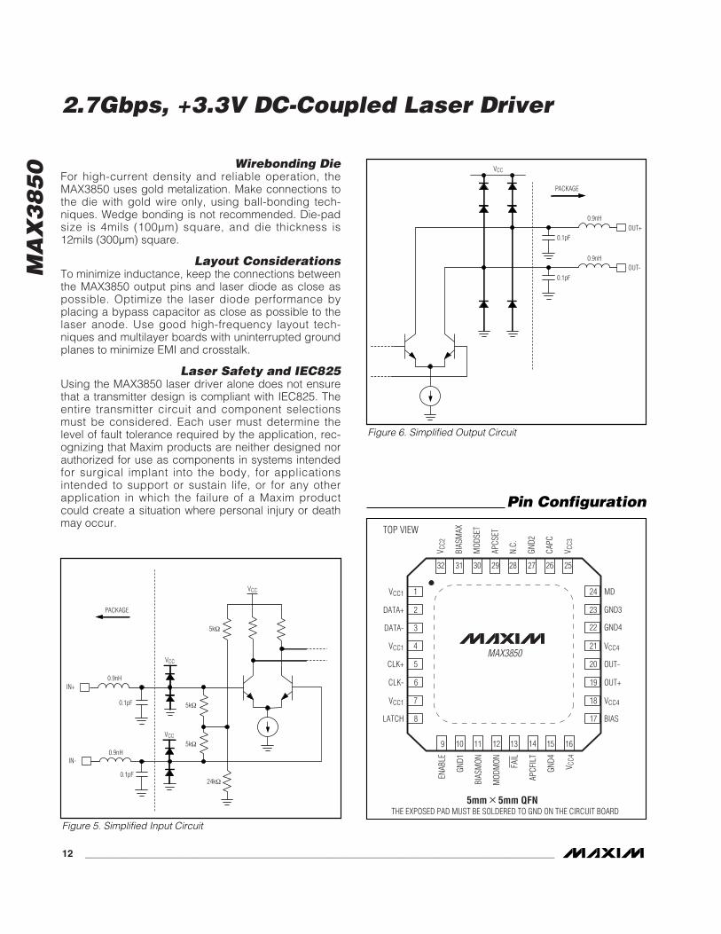
0 Wirebonding DieFor high-current density and reliable operation, theMAX3850 uses gold metalization. Make connections tothe die with gold wire only, using ball-bonding tech-niques. Wedge bonding is not recommended. Die-padsize is 4mils (100µm) square, and die thickness is12mils (300µm) square.
Layout ConsiderationsTo minimize inductance, keep the connections betweenthe MAX3850 output pins and laser diode as close aspossible. Optimize the laser diode performance byplacing a bypass capacitor as close as possible to thelaser anode. Use good high-frequency layout tech-niques and multilayer boards with uninterrupted groundplanes to minimize EMI and crosstalk.
Laser Safety and IEC825Using the MAX3850 laser driver alone does not ensurethat a transmitter design is compliant with IEC825. Theentire transmitter circuit and component selectionsmust be considered. Each user must determine thelevel of fault tolerance required by the application, rec-ognizing that Maxim products are neither designed norauthorized for use as components in systems intendedfor surgical implant into the body, for applicationsintended to support or sustain life, or for any otherapplication in which the failure of a Maxim productcould create a situation where personal injury or deathmay occur.
2.7Gbps, +3.3V DC-Coupled Laser Driver
12 ______________________________________________________________________________________
5mm 5mm QFN
MAX3850
TOP VIEW
32 28293031 252627
BIAS
MAX
MOD
SET
APCS
ET
N.C.
V CC2
GND2
CAPC
V CC3
10 13 1514 1611 129
ENAB
LE
BIAS
MON
GND1 FAIL
MOD
MON
GND4
APCF
ILT
V CC4
17
18
19
20
21
22
23 GND3
24 MD
GND4
VCC4
OUT-
OUT+
VCC4
BIAS
2
3
4
5
6
7
8LATCH
THE EXPOSED PAD MUST BE SOLDERED TO GND ON THE CIRCUIT BOARD
VCC1
CLK-
CLK+
VCC1
DATA-
DATA+
1VCC1
Pin Configuration
5kΩ
5kΩ
24kΩ
VCC
0.1pF
0.1pF
0.9nH
0.9nH
PACKAGE
IN+
IN-
5kΩ
VCC
VCC
Figure 5. Simplified Input Circuit
0.1pFOUT+
PACKAGE
0.9nH
VCC
OUT-0.9nH
0.1pF
Figure 6. Simplified Output Circuit
MA
X3
85
0
2.7Gbps, +3.3V DC-Coupled Laser Driver
______________________________________________________________________________________ 13
LATCH
CLK- VCC1 VCC1 DATA+
VCC1 CLK+ DATA-
ENABLE
GND1
GND1BIASMON
MODMON
FAILGND4
N.C.APCFILT
GND4VCC4
GND1
GND1
GND1
VCC1 GND2
MDGND4N.C.OUT+VCC4
OUT-N.C. N.C. GND3VCC4
BIAS
VCC2
BIASMAX
MODSET
GND2APCSET
N.C.GND3N.C.
GND3N.C.
CAPCVCC3
GND3
0.083"(2.108mm)
0.070"(1.778mm)
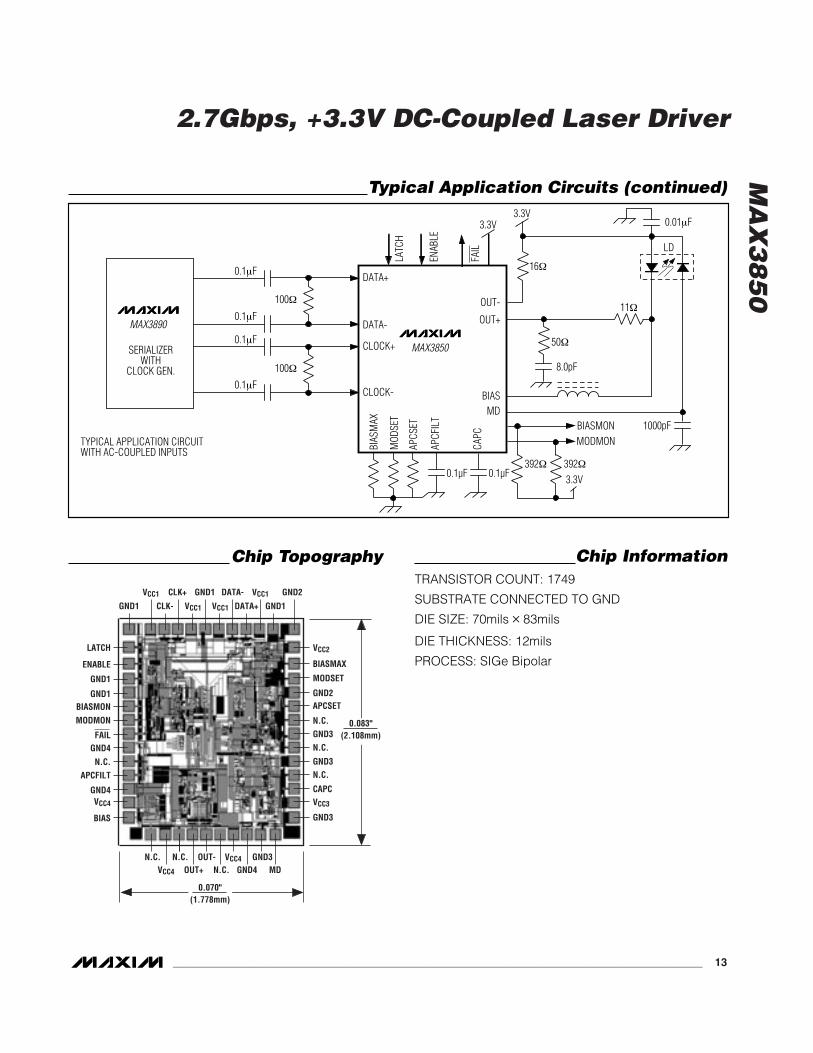
Chip Topography
SERIALIZERWITH
CLOCK GEN.
TYPICAL APPLICATION CIRCUITWITH AC-COUPLED INPUTS
11Ω
LD
16Ω
50Ω
392Ω392Ω
3.3V3.3V
8.0pF
0.1µF0.1µF
0.01µF
BIASMONMODMON
3.3V
1000pF
BIAS
MAX
LATC
H
ENAB
LE
FAIL
MOD
SET
APCS
ET
APCF
ILT
CLOCK-
CLOCK+
DATA-
DATA+
OUT+
BIASMD
OUT-
CAPC
MAX3850
MAX3890
0.1µF
0.1µF
0.1µF
0.1µF
100Ω
100Ω
Typical Application Circuits (continued)
Chip InformationTRANSISTOR COUNT: 1749
SUBSTRATE CONNECTED TO GND
DIE SIZE: 70mils 83mils
DIE THICKNESS: 12mils
PROCESS: SIGe Bipolar
MA
X3
85
0
2.7Gbps, +3.3V DC-Coupled Laser Driver
Maxim cannot assume responsibility for use of any circuitry other than circuitry entirely embodied in a Maxim product. No circuit patent licenses areimplied. Maxim reserves the right to change the circuitry and specifications without notice at any time.
14 ____________________Maxim Integrated Products, 120 San Gabriel Drive, Sunnyvale, CA 94086 408-737-7600
© 2003 Maxim Integrated Products Printed USA is a registered trademark of Maxim Integrated Products.
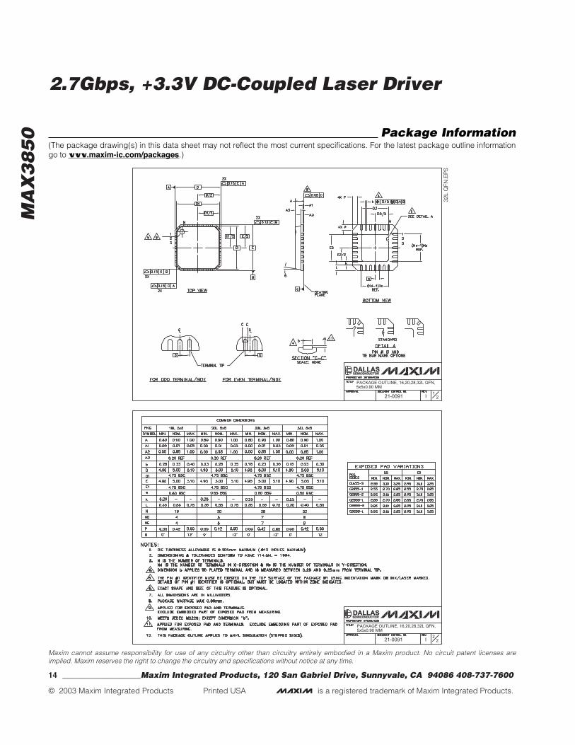
Package Information(The package drawing(s) in this data sheet may not reflect the most current specifications. For the latest package outline informationgo to www.maxim-ic.com/packages.)
32L
QFN
.EP
S