Embed Size (px)
Citation preview
FN8945 Rev.0.00 Page 1 of 75Oct 22, 2018
FN8945Rev.0.00
Oct 22, 2018
ISL9241Buck-Boost Configurable Battery Charger with SMBus Interface and USB Power Delivery
DATASHEET
The ISL9241 is a digitally configurable buck-boost battery charger that can support both Narrow Voltage Direct Charging (NVDC) and Hybrid Power Buck Boost (HPBB/Bypass) charging and switch between the modes using firmware control. Bypass mode is also supported using a controller’s firmware, allowing the adapter to provide power directly to the system. The ISL9241 provides the charging function, system bus regulation, and protection features using only NFETs for tablet, ultrabook, and notebook platforms. The advanced Renesas R3™ technology provides a high, light-load efficient Charging mode. The ISL9241 takes input power from a wide range of DC power sources (conventional AC/DC charger adapters, USB Type-C Power ports, travel adapters, etc.) and safely charges battery packs with up to 4-series cell Li-ion batteries.
The system power can be provided from the adapter, battery, or a combination of both. The ISL9241 reconfigurability of the compensation allows a smaller inductor and higher efficiencies optimized for multiple power levels. The ISL9241 can operate with only a battery, only an adapter, or both connected. For Intel IMVP compliant systems, the ISL9241 includes System Power monitor (PSYS) functionality, which provides an analog signal representing total platform power. The PSYS output connects to a wide range of IMVP core regulators to provide an IMVP compliant power domain function. The ISL9241 supports reverse buck, boost, or buck-boost operation to the adapter port (OTG mode) from 2- to 4-cell batteries. This allows configurations to support USB-C Power Delivery (PD) output for Programmable Power Supply (PPS) ports. The ISL9241 serial communication uses SMBus/I2C, which allows programming of many key parameters to deliver a customized solution.
Features• Buck-boost NVDC or hybrid power (turbo boost)
charger for 2-, 3-, or 4-cell Li-ion batteries using all NFET transistors
• Input voltage range: 3.9V to 23.4V (no dead zone)
• System/battery output voltage: 3.9V to 18.304V
• Bypass mode supported, to connect system to adapter
• Autonomous charging option (automatic end of charging)
• Adapter current and battery current monitor (AMON/BMON)
• PROCHOT# open-drain output, IMVP compliant
• System power monitor PSYS output, IMVP8/9 compliant
• Internal 8-bit ADC for monitoring key parameters
• USB-C PD Fast Role Swap support and PPS support
• Independent compensation pins for forward and reverse operation (OTG) modes
• Supports supplemental power (Intel VMIN active protection)
• Battery Ship mode - IC ultra-low power state
• Supports JEITA compliance using an NTC
• 4x4 32 Ld TQFN package
Applications• 2- to 4-cell tablets, notebooks, power banks, and any
USB-C interface portable device requiring batteries
Related LiteratureFor a full list of related documents visit our website
• ISL9241 product page
Figure 1. Typical Application
VSYSVIN
BYPSG
BGATE
NGATEQ1
Q3Q2
Q4
CIN
CBAT
COUT
FN8945 Rev.0.00 Page 2 of 75Oct 22, 2018
ISL9241
Contents
1. Overview. . . . . . . . . . . . . . . . . . . . . . . . . . . . . . . . . . . . . . . . . . . . . . . . . . . . . . . . . . . . . . . . . . . . . 4
1.1 Simplified Application Circuits . . . . . . . . . . . . . . . . . . . . . . . . . . . . . . . . . . . . . . . . . . . . . . . . . . 4
1.2 Block Diagram . . . . . . . . . . . . . . . . . . . . . . . . . . . . . . . . . . . . . . . . . . . . . . . . . . . . . . . . . . . . . . 6
1.3 Ordering Information . . . . . . . . . . . . . . . . . . . . . . . . . . . . . . . . . . . . . . . . . . . . . . . . . . . . . . . . . 7
1.4 Pin Configuration . . . . . . . . . . . . . . . . . . . . . . . . . . . . . . . . . . . . . . . . . . . . . . . . . . . . . . . . . . . . 8
1.5 Pin Descriptions. . . . . . . . . . . . . . . . . . . . . . . . . . . . . . . . . . . . . . . . . . . . . . . . . . . . . . . . . . . . . 8
2. Specifications. . . . . . . . . . . . . . . . . . . . . . . . . . . . . . . . . . . . . . . . . . . . . . . . . . . . . . . . . . . . . . . . 11
2.1 Absolute Maximum Ratings . . . . . . . . . . . . . . . . . . . . . . . . . . . . . . . . . . . . . . . . . . . . . . . . . . . 11
2.2 Thermal Information. . . . . . . . . . . . . . . . . . . . . . . . . . . . . . . . . . . . . . . . . . . . . . . . . . . . . . . . . 12
2.3 Recommended Operation Conditions . . . . . . . . . . . . . . . . . . . . . . . . . . . . . . . . . . . . . . . . . . . 12
2.4 Electrical Specifications . . . . . . . . . . . . . . . . . . . . . . . . . . . . . . . . . . . . . . . . . . . . . . . . . . . . . . 12
2.5 SMBus Timing Specification . . . . . . . . . . . . . . . . . . . . . . . . . . . . . . . . . . . . . . . . . . . . . . . . . . 19
2.6 Gate Driver Timing Diagram . . . . . . . . . . . . . . . . . . . . . . . . . . . . . . . . . . . . . . . . . . . . . . . . . . 19
3. Typical Performance . . . . . . . . . . . . . . . . . . . . . . . . . . . . . . . . . . . . . . . . . . . . . . . . . . . . . . . . . . 20
4. General SMBus Architecture . . . . . . . . . . . . . . . . . . . . . . . . . . . . . . . . . . . . . . . . . . . . . . . . . . . 24
4.1 Data Validity . . . . . . . . . . . . . . . . . . . . . . . . . . . . . . . . . . . . . . . . . . . . . . . . . . . . . . . . . . . . . . . 24
4.2 START and STOP Conditions . . . . . . . . . . . . . . . . . . . . . . . . . . . . . . . . . . . . . . . . . . . . . . . . . 24
4.3 Acknowledge . . . . . . . . . . . . . . . . . . . . . . . . . . . . . . . . . . . . . . . . . . . . . . . . . . . . . . . . . . . . . . 25
4.4 SMBus Transactions . . . . . . . . . . . . . . . . . . . . . . . . . . . . . . . . . . . . . . . . . . . . . . . . . . . . . . . . 25
4.5 Byte Format . . . . . . . . . . . . . . . . . . . . . . . . . . . . . . . . . . . . . . . . . . . . . . . . . . . . . . . . . . . . . . . 25
4.6 SMBus and I2C Compatibility . . . . . . . . . . . . . . . . . . . . . . . . . . . . . . . . . . . . . . . . . . . . . . . . . 25
4.7 ISL9241 SMBus Commands . . . . . . . . . . . . . . . . . . . . . . . . . . . . . . . . . . . . . . . . . . . . . . . . . . 26
5. ISL9241 Registers . . . . . . . . . . . . . . . . . . . . . . . . . . . . . . . . . . . . . . . . . . . . . . . . . . . . . . . . . . . . 27
5.1 Register Summary . . . . . . . . . . . . . . . . . . . . . . . . . . . . . . . . . . . . . . . . . . . . . . . . . . . . . . . . . . 27
5.2 DAC Register Summary . . . . . . . . . . . . . . . . . . . . . . . . . . . . . . . . . . . . . . . . . . . . . . . . . . . . . 29
5.3 Control Registers . . . . . . . . . . . . . . . . . . . . . . . . . . . . . . . . . . . . . . . . . . . . . . . . . . . . . . . . . . . 30
5.4 Interrupt Functionality . . . . . . . . . . . . . . . . . . . . . . . . . . . . . . . . . . . . . . . . . . . . . . . . . . . . . . . 36
5.5 Information Register . . . . . . . . . . . . . . . . . . . . . . . . . . . . . . . . . . . . . . . . . . . . . . . . . . . . . . . . 38
5.6 ADC Registers . . . . . . . . . . . . . . . . . . . . . . . . . . . . . . . . . . . . . . . . . . . . . . . . . . . . . . . . . . . . . 40
6. Application Information. . . . . . . . . . . . . . . . . . . . . . . . . . . . . . . . . . . . . . . . . . . . . . . . . . . . . . . . 41
6.1 Start-Up and ACOK . . . . . . . . . . . . . . . . . . . . . . . . . . . . . . . . . . . . . . . . . . . . . . . . . . . . . . . . . 41
6.2 Programming Resistor . . . . . . . . . . . . . . . . . . . . . . . . . . . . . . . . . . . . . . . . . . . . . . . . . . . . . . . 42
6.3 Charger Control Register Operations . . . . . . . . . . . . . . . . . . . . . . . . . . . . . . . . . . . . . . . . . . . 43
6.4 Reverse Modes . . . . . . . . . . . . . . . . . . . . . . . . . . . . . . . . . . . . . . . . . . . . . . . . . . . . . . . . . . . . 48
6.5 Monitoring . . . . . . . . . . . . . . . . . . . . . . . . . . . . . . . . . . . . . . . . . . . . . . . . . . . . . . . . . . . . . . . . 51
6.6 Protection. . . . . . . . . . . . . . . . . . . . . . . . . . . . . . . . . . . . . . . . . . . . . . . . . . . . . . . . . . . . . . . . . 54
6.7 Additional Features . . . . . . . . . . . . . . . . . . . . . . . . . . . . . . . . . . . . . . . . . . . . . . . . . . . . . . . . . 55
FN8945 Rev.0.00 Page 3 of 75Oct 22, 2018
ISL9241
7. Modulator Information. . . . . . . . . . . . . . . . . . . . . . . . . . . . . . . . . . . . . . . . . . . . . . . . . . . . . . . . . 57
7.1 ISL9241 Buck-Boost Charger Modes of Operation . . . . . . . . . . . . . . . . . . . . . . . . . . . . . . . . . 57
7.2 Modulator Control Loops . . . . . . . . . . . . . . . . . . . . . . . . . . . . . . . . . . . . . . . . . . . . . . . . . . . . . 58
7.3 Buck Boost Configurable Charger . . . . . . . . . . . . . . . . . . . . . . . . . . . . . . . . . . . . . . . . . . . . . . 61
7.4 R3 Modulator . . . . . . . . . . . . . . . . . . . . . . . . . . . . . . . . . . . . . . . . . . . . . . . . . . . . . . . . . . . . . . 64
8. Design Guide . . . . . . . . . . . . . . . . . . . . . . . . . . . . . . . . . . . . . . . . . . . . . . . . . . . . . . . . . . . . . . . . 67
8.1 Selecting the Sense Resistors. . . . . . . . . . . . . . . . . . . . . . . . . . . . . . . . . . . . . . . . . . . . . . . . . 67
8.2 Selecting the LC Output Filter . . . . . . . . . . . . . . . . . . . . . . . . . . . . . . . . . . . . . . . . . . . . . . . . . 67
8.3 Adapter Input Filter . . . . . . . . . . . . . . . . . . . . . . . . . . . . . . . . . . . . . . . . . . . . . . . . . . . . . . . . . 68
8.4 Select the Input Capacitor . . . . . . . . . . . . . . . . . . . . . . . . . . . . . . . . . . . . . . . . . . . . . . . . . . . . 68
8.5 Select the Switching Power MOSFET . . . . . . . . . . . . . . . . . . . . . . . . . . . . . . . . . . . . . . . . . . . 69
8.6 Select the Bootstrap Capacitor . . . . . . . . . . . . . . . . . . . . . . . . . . . . . . . . . . . . . . . . . . . . . . . . 70
9. Layout . . . . . . . . . . . . . . . . . . . . . . . . . . . . . . . . . . . . . . . . . . . . . . . . . . . . . . . . . . . . . . . . . . . . . . 71
10. Revision History. . . . . . . . . . . . . . . . . . . . . . . . . . . . . . . . . . . . . . . . . . . . . . . . . . . . . . . . . . . . . . 73
11. Package Outline Drawing . . . . . . . . . . . . . . . . . . . . . . . . . . . . . . . . . . . . . . . . . . . . . . . . . . . . . . 74
FN8945 Rev.0.00 Page 4 of 75Oct 22, 2018
ISL9241 1. Overview
1. Overview
1.1 Simplified Application Circuits
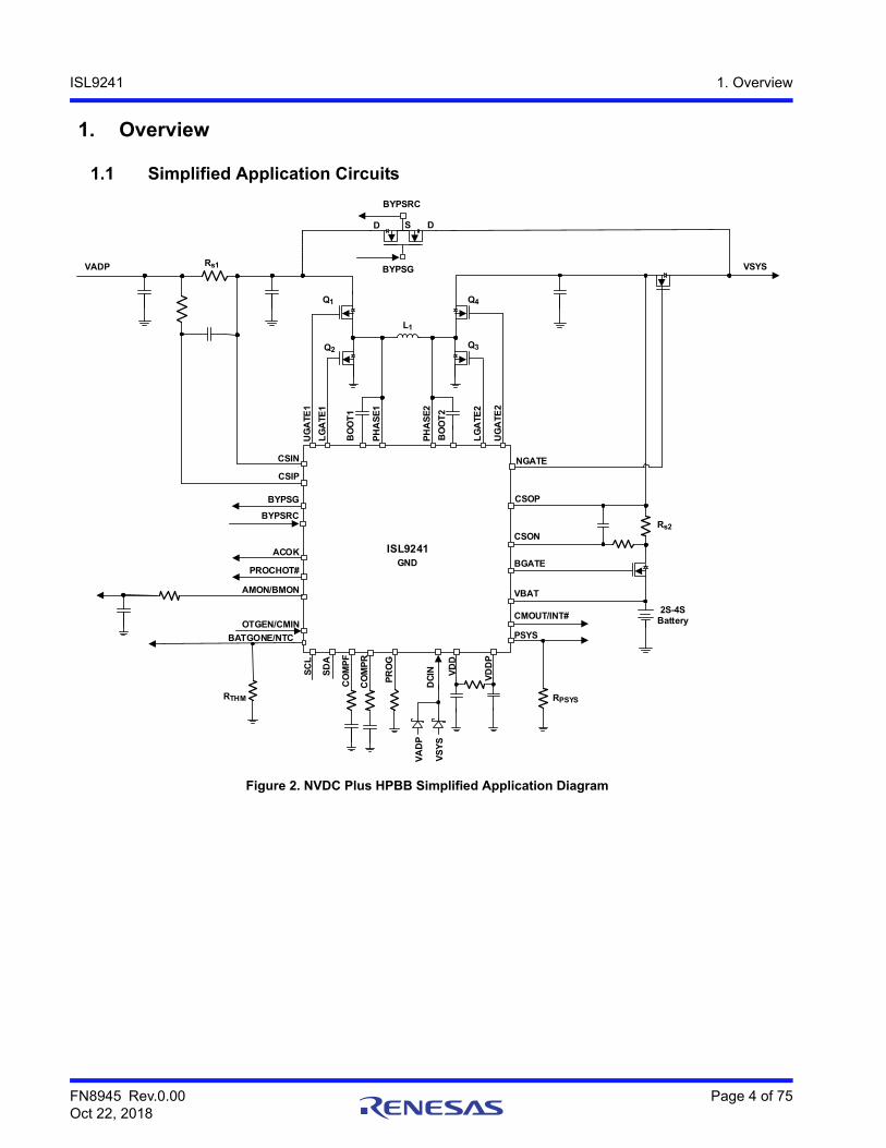
Figure 2. NVDC Plus HPBB Simplified Application Diagram
ISL9241
BO
OT
1
PH
AS
E1
UG
ATE
1
VD
DP
LG
ATE
1
LG
ATE
2
UG
ATE
2
PH
AS
E2
BO
OT
2
SC
L
SD
A
VBAT
CSOP
CSON
DC
IN VD
D
CO
MP
F
PSYS
BGATEPROCHOT#
ACOK
GND
CSIP
CSIN
AMON/BMON
VADP
2S-4S
Battery
PR
OG
CMOUT/INT#OTGEN/CMIN
Q1
Q2
Q4
Q3
Rs1
Rs2
L1
BATGONE/NTC
NGATE
VSYS
BYPSRC
RTHM
VS
YS
VA
DP
BYPSG
S DD
BYPSG
BYPSRC
CO
MP
R
RPSYS
FN8945 Rev.0.00 Page 5 of 75Oct 22, 2018
ISL9241 1. Overview
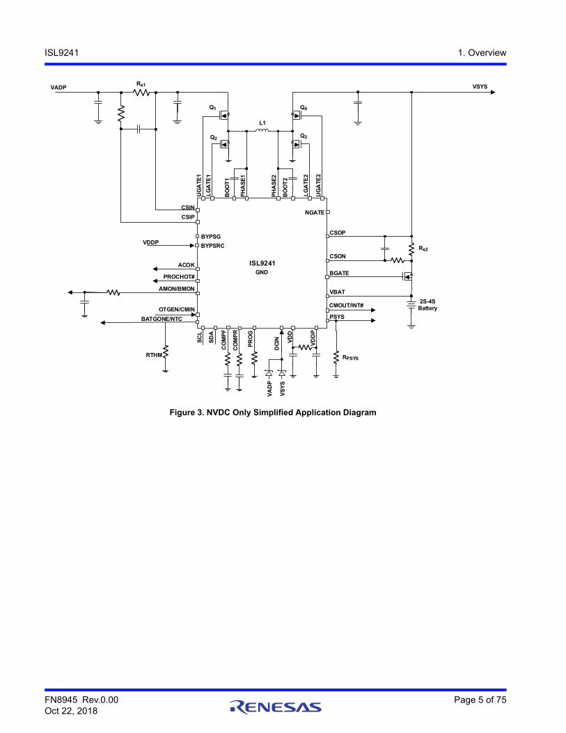
Figure 3. NVDC Only Simplified Application Diagram
ISL9241
BO
OT
1
PH
AS
E1
UG
ATE
1
VD
DP
LG
ATE
1
LG
ATE
2
UG
ATE
2
PH
AS
E2
BO
OT
2
SC
L
SD
A
VBAT
CSOP
CSON
DC
IN VD
D
PSYS
BGATEPROCHOT#
ACOK
GND
CSIP
CSIN
AMON/BMON
VADP
2S-4S
Battery
PR
OG
CMOUT/INT#OTGEN/CMIN
Q1
Q2
Q4
Q3
Rs1
Rs2
L1
BATGONE/NTC
NGATE
VSYS
RTHM
VS
YS
VA
DP
BYPSG
BYPSRC
RPSYS
CO
MP
F
CO
MP
R
VDDP
FN8945 Rev.0.00 Page 6 of 75Oct 22, 2018
ISL9241 1. Overview
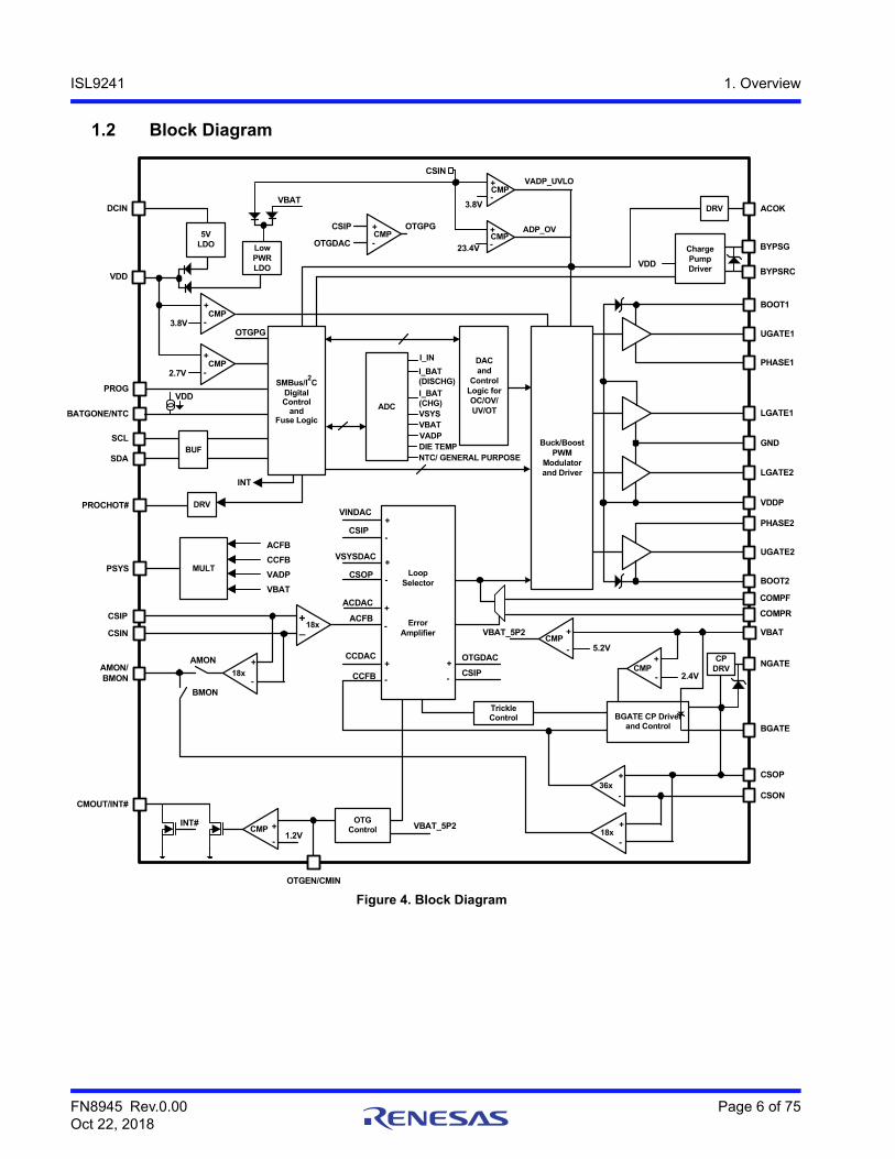
1.2 Block Diagram
Figure 4. Block Diagram
PROG
SCL
SMBus/I2C
Digital Control
andFuse Logic
DACand
Control Logic for OC/OV/UV/OT
5V LDO
BGATE CP Driver and Control
Buck/Boost PWM
Modulatorand Driver
DRV
CSON
CSOP
AMON/BMON
CSIN
CSIP
VDD
SDA
DCIN ACOK
BOOT1
UGATE1
PHASE1
LGATE1
GND
LGATE2
VDDP
PHASE2
UGATE2
BOOT2
COMPF
BGATE
18x
+_18x
CSOP
DRVPROCHOT#
BUF
CMOUT/INT#
VBAT
VSYSDAC
ACDAC
LoopSelector
ErrorAmplifier
ACFB
CCDAC
CCFB
BATGONE/NTC
18x
36x
BMON
AMON
CSIP
VINDAC
CSIP
Low PWR LDO
VBAT
CMP
CMP
1.2V
OTGEN/CMIN
OTGDAC
OTGControl
Trickle Control
CMP
3.8V
CMP
CMP
3.8V
2.7V
OTGDAC
CSIPCMP
CMP
2.4V
5.2V
VBAT_5P2
VBAT_5P2
+
+
-
-
++
- -
+
+
-
+
-
-
+
+
-
-
+
+
+
-
-
-
-
-
+
+
+
-
PSYS MULT
ACFB
CCFB
VADP
VBAT
ADC
VBATVADPDIE TEMPNTC/ GENERAL PURPOSE
VSYS
I_BAT (CHG)
I_IN
NGATE
BYPSG
BYPSRC
CP DRV
Charge Pump Driver
VDD
VDD
CSIN
INT#
INT
I_BAT (DISCHG)
CMP+
-23.4V
ADP_OV
VADP_UVLO
COMPR
OTGPG
OTGPG
FN8945 Rev.0.00 Page 7 of 75Oct 22, 2018
ISL9241 1. Overview
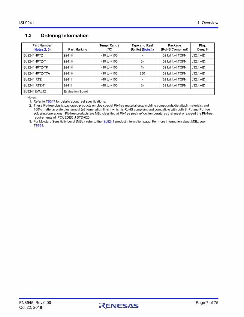
1.3 Ordering Information
Part Number(Notes 2, 3) Part Marking
Temp. Range(°C)
Tape and Reel(Units) (Note 1)
Package(RoHS Compliant)
Pkg.Dwg. #
ISL9241HRTZ 9241H -10 to +100 - 32 Ld 4x4 TQFN L32.4x4D
ISL9241HRTZ-T 9241H -10 to +100 6k 32 Ld 4x4 TQFN L32.4x4D
ISL9241HRTZ-TK 9241H -10 to +100 1k 32 Ld 4x4 TQFN L32.4x4D
ISL9241HRTZ-T7A 9241H -10 to +100 250 32 Ld 4x4 TQFN L32.4x4D
ISL9241IRTZ 9241I -40 to +100 - 32 Ld 4x4 TQFN L32.4x4D
ISL9241IRTZ-T 9241I -40 to +100 6k 32 Ld 4x4 TQFN L32.4x4D
ISL9241EVAL1Z Evaluation Board
Notes:1. Refer to TB347 for details about reel specifications.2. These Pb-free plastic packaged products employ special Pb-free material sets, molding compounds/die attach materials, and
100% matte tin plate plus anneal (e3 termination finish, which is RoHS compliant and compatible with both SnPb and Pb-free soldering operations). Pb-free products are MSL classified at Pb-free peak reflow temperatures that meet or exceed the Pb-free requirements of IPC/JEDEC J STD-020.
3. For Moisture Sensitivity Level (MSL), refer to the ISL9241 product information page. For more information about MSL, see TB363.
FN8945 Rev.0.00 Page 8 of 75Oct 22, 2018
ISL9241 1. Overview
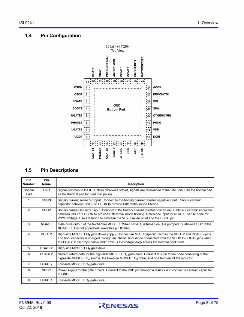
1.4 Pin Configuration
1.5 Pin Descriptions
32 Ld 4x4 TQFNTop View
PinNumber
PinName Description
BottomPad
GND Signal common to the IC. Unless otherwise stated, signals are referenced to the GND pin. Use the bottom pad as the thermal pad for heat dissipation.
1 CSON Battery current sense “–” input. Connect to the battery current resistor negative input. Place a ceramic capacitor between CSOP to CSON to provide Differential mode filtering.
2 CSOP Battery current sense “+” input. Connect to the battery current resistor positive input. Place a ceramic capacitor between CSOP to CSON to provide Differential mode filtering. Reference input for NGATE. Sense node for VSYS voltage. Use a Kelvin line between the VSYS sense point and the CSOP pin.
3 NGATE Gate drive output of the N-channel MOSFET. When NGATE is turned on, it is pumped 5V above CSOP. If the NGATE FET is not populated, leave this pin floating.
4 BOOT2 High-side MOSFET Q4 gate driver supply. Connect an MLCC capacitor across the BOOT2 and PHASE2 pins. The boot capacitor is charged through an internal boot diode connected from the VDDP to BOOT2 pins when the PHASE2 pin drops below VDDP minus the voltage drop across the internal boot diode.
5 UGATE2 High-side MOSFET Q4 gate drive.
6 PHASE2 Current return path for the high-side MOSFET Q4 gate drive. Connect this pin to the node consisting of the high-side MOSFET Q4 source, the low-side MOSFET Q3 drain, and one terminal of the inductor.
7 LGATE2 Low-side MOSFET Q3 gate drive.
8 VDDP Power supply for the gate drivers. Connect to the VDD pin through a resistor and connect a ceramic capacitor to GND.
9 LGATE1 Low-side MOSFET Q2 gate drive.
BG
AT
E
VB
AT
PS
YS
/(R
EF
AD
J)
AM
ON
/BM
ON
CO
MP
F
CO
MP
R
CM
OU
T/IN
T#
BA
TG
ON
E/N
TC
LG
AT
E1
PH
AS
E1
UG
AT
E1
BO
OT
1
BY
PS
RC
CS
IN
CS
IP
BY
PS
G
CSON
CSOP
NGATE
BOOT2
UGATE2
PHASE2
LGATE2
VDDP
ACOK
PROCHOT#
SCL
SDA
OTGEN/CMIN
PROG
VDD
DCIN
1
2
3
4
5
6
7
8
24
23
22
21
20
19
18
17
32 31 30 29 28 27 26 25
9 10 11 12 13 14 15 16
GNDBottom Pad
FN8945 Rev.0.00 Page 9 of 75Oct 22, 2018
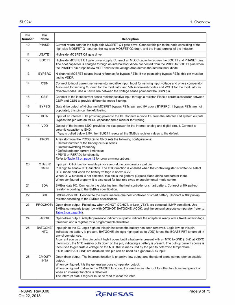
ISL9241 1. Overview
10 PHASE1 Current return path for the high-side MOSFET Q1 gate drive. Connect this pin to the node consisting of the high-side MOSFET Q1 source, the low-side MOSFET Q2 drain, and the input terminal of the inductor.
11 UGATE1 High-side MOSFET Q1 gate drive.
12 BOOT1 High-side MOSFET Q1 gate driver supply. Connect an MLCC capacitor across the BOOT1 and PHASE1 pins. The boot capacitor is charged through an internal boot diode connected from the VDDP to BOOT1 pins when the PHASE1 pin drops below VDDP minus the voltage drop across the internal boot diode.
13 BYPSRC N-channel MOSFET source input reference for bypass FETs. If not populating bypass FETs, this pin must be tied to VDDP.
14 CSIN Connect to input current sense resistor negative input. Input for sensing input voltage and phase comparator. Also used for sensing Q1 drain for the modulator and VIN in forward-modes and VOUT for the modulator in reverse-modes. Use a Kelvin line between the voltage sense point and the CSIN pin.
15 CSIP Connect to the input current sense resistor positive input through a resistor. Place a ceramic capacitor between CSIP and CSIN to provide differential-mode filtering.
16 BYPSG Gate drive output of N-channel MOSFET bypass FETs, pumped 5V above BYPSRC. If bypass FETs are not populated, this pin can be left floating.
17 DCIN Input of an internal LDO providing power to the IC. Connect a diode OR from the adapter and system outputs. Bypass this pin with an MLCC capacitor and a resistor for filtering.
18 VDD Output of the internal LDO; provides the bias power for the internal analog and digital circuit. Connect a ceramic capacitor to GND.If VDD is pulled below 2.5V, the ISL9241 resets all the SMBus register values to the default.
19 PROG A resistor from the PROG pin to GND sets the following configurations: • Default number of the battery cells in series• Default switching frequency• Default adapter current limit value• PSYS or REFADJ functionalityRefer to Table 13 on page 42 for programming options.
20 OTGEN/CMIN
Input pin. OTG function enable pin or stand-alone comparator input pin. Pull high to enable OTG function. The OTG function is enabled when the control register is written to select OTG mode and when the battery voltage is above 5.2V.When OTG function is not selected, this pin is the general purpose stand-alone comparator input. When configured properly, it is also used for fast role swap or supplemental mode control.
21 SDA SMBus data I/O. Connect to the data line from the host controller or smart battery. Connect a 10k pull-up resistor according to the SMBus specification.
22 SCL SMBus clock I/O. Connect to the clock line from the host controller or smart battery. Connect a 10k pull-up resistor according to the SMBus specification.
23 PROCHOT# Open-drain output. Pulled low when ACHOT, DCHOT, or Low_VSYS are detected. IMVP compliant. Use SMBus commands to pull low with OTGHOT, BATGONE, ACOK, and the general purpose comparator (refer to Table 6 on page 34).
24 ACOK Open-drain output. Adapter presence indicator output to indicate the adapter is ready with a fixed undervoltage threshold and a register for a programmable threshold.
25 BATGONE/NTC
Input pin to the IC. Logic high on this pin indicates the battery has been removed. Logic low on this pin indicates the battery is present. BATGONE pin logic high (pull up to VDD) forces the BGATE FET to turn off in any circumstances.A current source on this pin pulls it high if open, but if a battery is present with an NTC to GND (10kΩ at +25°C thermistor), the NTC resistor pulls down on the pin, indicating a battery is present. The pull-up current source is then used to generate a voltage on the NTC that is measured by the part to determine temperature.If NTC and BATGONE are disabled, this pin can be used as a general ADC input.
26 CMOUT/INT#
Open-drain output. The interrupt function is an active-low output and the stand-alone comparator selectable output. When configured, it is the general purpose comparator output.When configured to disable the CMOUT function, it is used as an interrupt for other functions and goes low when an interrupt function is detected. The interrupt status register must be read to clear the latch.
PinNumber
PinName Description
FN8945 Rev.0.00 Page 10 of 75Oct 22, 2018
ISL9241 1. Overview
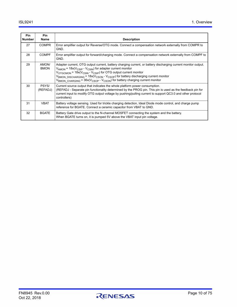
27 COMPR Error amplifier output for Reverse/OTG mode. Connect a compensation network externally from COMPR to GND.
28 COMPF Error amplifier output for forward/charging mode. Connect a compensation network externally from COMPF to GND.
29 AMON/BMON
Adapter current, OTG output current, battery charging current, or battery discharging current monitor output. VAMON = 18x(VCSIP - VCSIN) for adapter current monitorVOTGCMON = 18x(VCSIN - VCSIP) for OTG output current monitorVBMON_DISCHARGING = 18x(VCSON - VCSOP) for battery discharging current monitorVBMON_CHARGING = 36x(VCSOP - VCSON) for battery charging current monitor
30 PSYS/(REFADJ)
Current source output that indicates the whole platform power consumption.(REFADJ - Separate pin functionality determined by the PROG pin. This pin is used as the feedback pin for current input to modify OTG output voltage by pushing/pulling current to support QC3.0 and other protocol controllers)
31 VBAT Battery voltage sensing. Used for trickle charging detection, Ideal Diode mode control, and charge pump reference for BGATE. Connect a ceramic capacitor from VBAT to GND.
32 BGATE Battery Gate drive output to the N-channel MOSFET connecting the system and the battery.When BGATE turns on, it is pumped 5V above the VBAT input pin voltage.
PinNumber
PinName Description
FN8945 Rev.0.00 Page 11 of 75Oct 22, 2018
ISL9241 2. Specifications
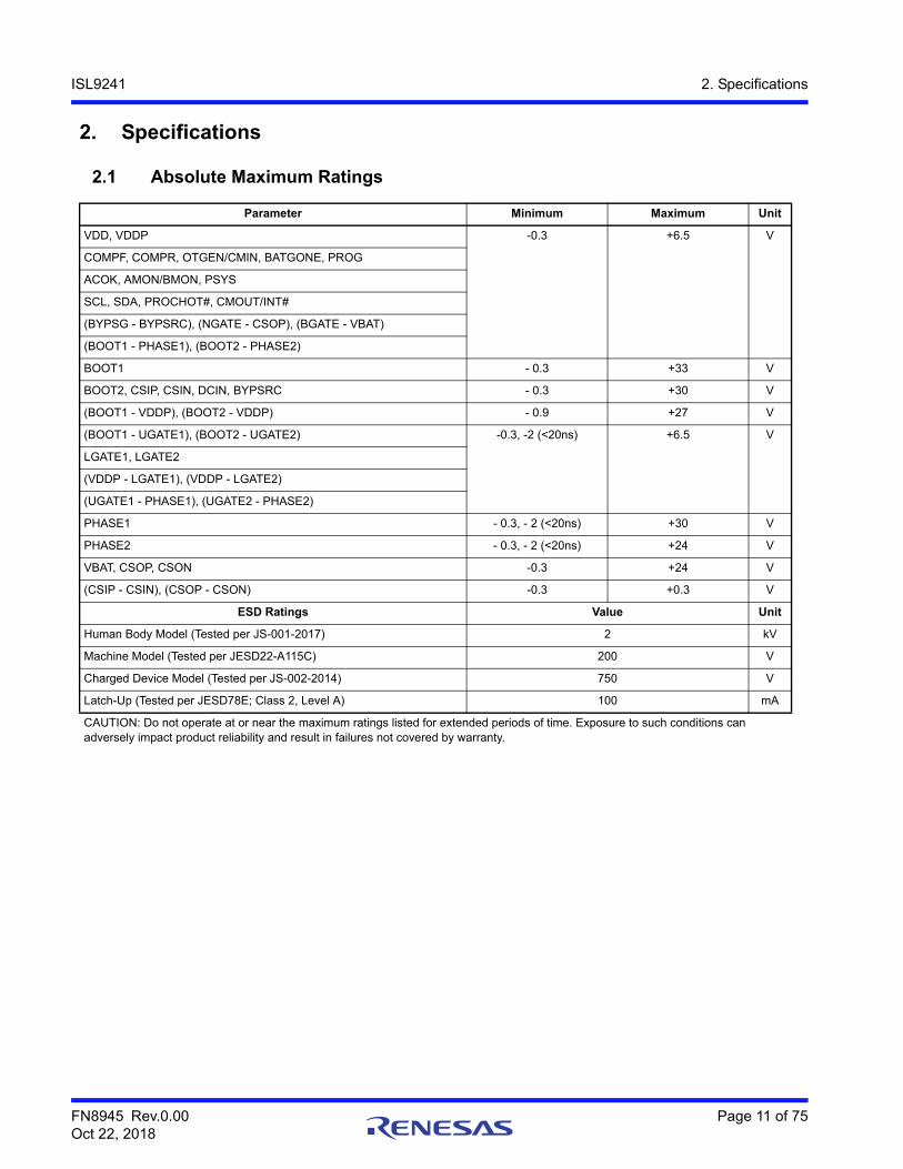
2. Specifications
2.1 Absolute Maximum Ratings
Parameter Minimum Maximum Unit
VDD, VDDP -0.3 +6.5 V
COMPF, COMPR, OTGEN/CMIN, BATGONE, PROG
ACOK, AMON/BMON, PSYS
SCL, SDA, PROCHOT#, CMOUT/INT#
(BYPSG - BYPSRC), (NGATE - CSOP), (BGATE - VBAT)
(BOOT1 - PHASE1), (BOOT2 - PHASE2)
BOOT1 - 0.3 +33 V
BOOT2, CSIP, CSIN, DCIN, BYPSRC - 0.3 +30 V
(BOOT1 - VDDP), (BOOT2 - VDDP) - 0.9 +27 V
(BOOT1 - UGATE1), (BOOT2 - UGATE2) -0.3, -2 (<20ns) +6.5 V
LGATE1, LGATE2
(VDDP - LGATE1), (VDDP - LGATE2)
(UGATE1 - PHASE1), (UGATE2 - PHASE2)
PHASE1 - 0.3, - 2 (<20ns) +30 V
PHASE2 - 0.3, - 2 (<20ns) +24 V
VBAT, CSOP, CSON -0.3 +24 V
(CSIP - CSIN), (CSOP - CSON) -0.3 +0.3 V
ESD Ratings Value Unit
Human Body Model (Tested per JS-001-2017) 2 kV
Machine Model (Tested per JESD22-A115C) 200 V
Charged Device Model (Tested per JS-002-2014) 750 V
Latch-Up (Tested per JESD78E; Class 2, Level A) 100 mA
CAUTION: Do not operate at or near the maximum ratings listed for extended periods of time. Exposure to such conditions can adversely impact product reliability and result in failures not covered by warranty.
FN8945 Rev.0.00 Page 12 of 75Oct 22, 2018
ISL9241 2. Specifications
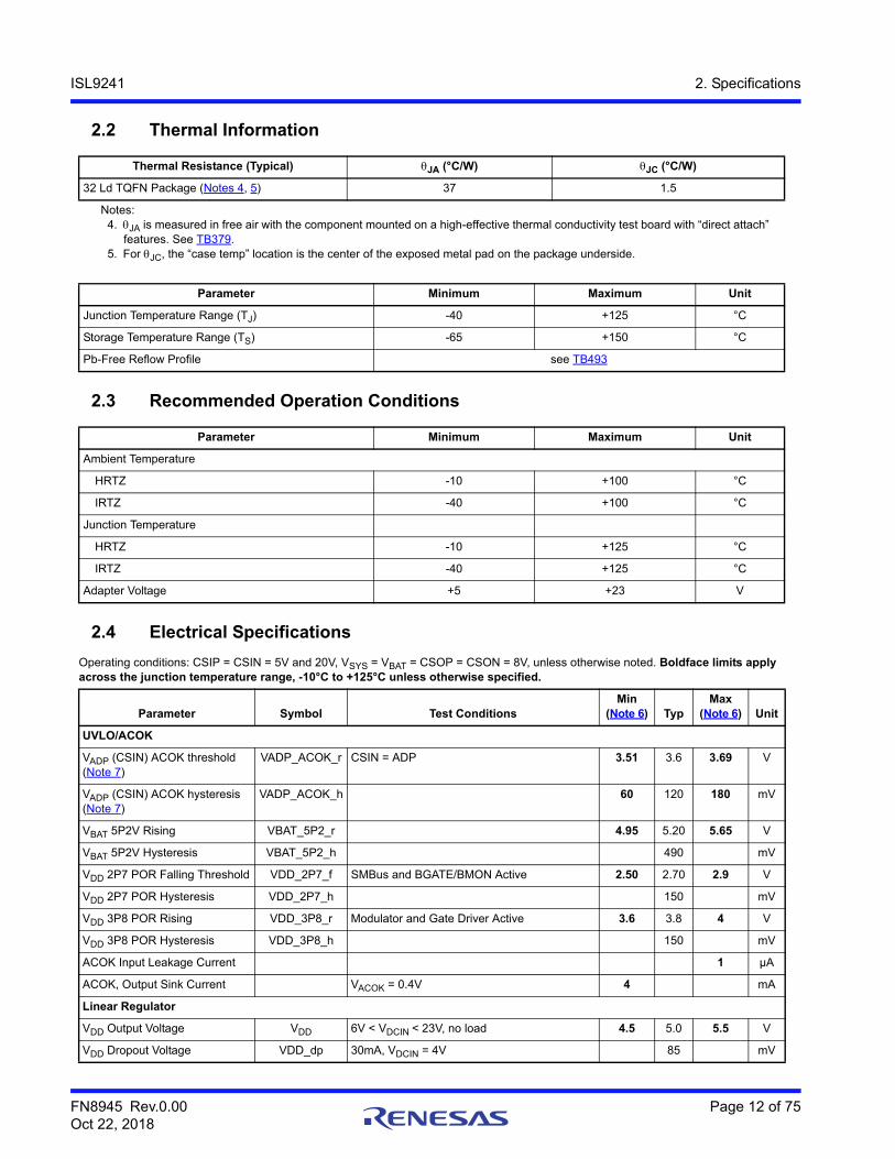
2.2 Thermal Information
2.3 Recommended Operation Conditions
2.4 Electrical Specifications
Thermal Resistance (Typical) JA (°C/W) JC (°C/W)
32 Ld TQFN Package (Notes 4, 5) 37 1.5
Notes:4. JA is measured in free air with the component mounted on a high-effective thermal conductivity test board with “direct attach”
features. See TB379.5. For JC, the “case temp” location is the center of the exposed metal pad on the package underside.
Parameter Minimum Maximum Unit
Junction Temperature Range (TJ) -40 +125 °C
Storage Temperature Range (TS) -65 +150 °C
Pb-Free Reflow Profile see TB493
Parameter Minimum Maximum Unit
Ambient Temperature
HRTZ -10 +100 °C
IRTZ -40 +100 °C
Junction Temperature
HRTZ -10 +125 °C
IRTZ -40 +125 °C
Adapter Voltage +5 +23 V
Operating conditions: CSIP = CSIN = 5V and 20V, VSYS = VBAT = CSOP = CSON = 8V, unless otherwise noted. Boldface limits apply across the junction temperature range, -10°C to +125°C unless otherwise specified.
Parameter Symbol Test ConditionsMin
(Note 6) TypMax
(Note 6) Unit
UVLO/ACOK
VADP (CSIN) ACOK threshold(Note 7)
VADP_ACOK_r CSIN = ADP 3.51 3.6 3.69 V
VADP (CSIN) ACOK hysteresis(Note 7)
VADP_ACOK_h 60 120 180 mV
VBAT 5P2V Rising VBAT_5P2_r 4.95 5.20 5.65 V
VBAT 5P2V Hysteresis VBAT_5P2_h 490 mV
VDD 2P7 POR Falling Threshold VDD_2P7_f SMBus and BGATE/BMON Active 2.50 2.70 2.9 V
VDD 2P7 POR Hysteresis VDD_2P7_h 150 mV
VDD 3P8 POR Rising VDD_3P8_r Modulator and Gate Driver Active 3.6 3.8 4 V
VDD 3P8 POR Hysteresis VDD_3P8_h 150 mV
ACOK Input Leakage Current 1 µA
ACOK, Output Sink Current VACOK = 0.4V 4 mA
Linear Regulator
VDD Output Voltage VDD 6V < VDCIN < 23V, no load 4.5 5.0 5.5 V
VDD Dropout Voltage VDD_dp 30mA, VDCIN = 4V 85 mV
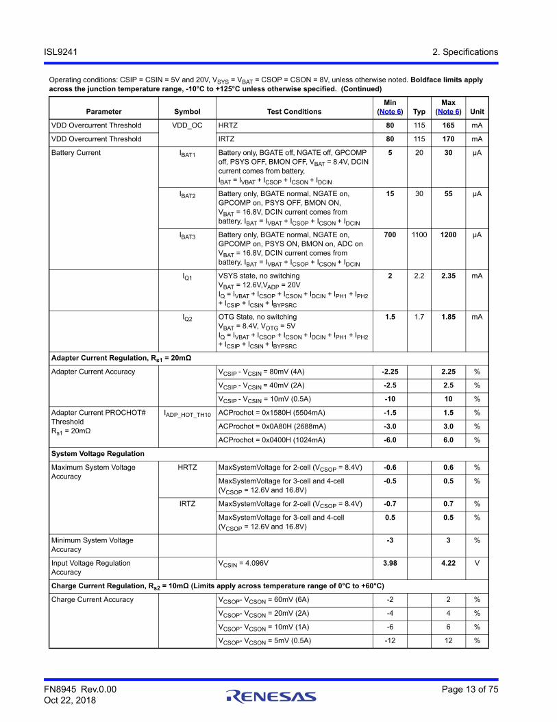
FN8945 Rev.0.00 Page 13 of 75Oct 22, 2018
ISL9241 2. Specifications
VDD Overcurrent Threshold VDD_OC HRTZ 80 115 165 mA
VDD Overcurrent Threshold IRTZ 80 115 170 mA
Battery Current IBAT1 Battery only, BGATE off, NGATE off, GPCOMP off, PSYS OFF, BMON OFF, VBAT = 8.4V, DCIN current comes from battery, IBAT = IVBAT + ICSOP + ICSON + IDCIN
5 20 30 µA
IBAT2 Battery only, BGATE normal, NGATE on, GPCOMP on, PSYS OFF, BMON ON, VBAT = 16.8V, DCIN current comes from battery, IBAT = IVBAT + ICSOP + ICSON + IDCIN
15 30 55 µA
IBAT3 Battery only, BGATE normal, NGATE on, GPCOMP on, PSYS ON, BMON on, ADC on VBAT = 16.8V, DCIN current comes from battery, IBAT = IVBAT + ICSOP + ICSON + IDCIN
700 1100 1200 µA
IQ1 VSYS state, no switching VBAT = 12.6V,VADP = 20V IQ = IVBAT + ICSOP + ICSON + IDCIN + IPH1 + IPH2 + ICSIP + ICSIN + IBYPSRC
2 2.2 2.35 mA
IQ2 OTG State, no switchingVBAT = 8.4V, VOTG = 5VIQ = IVBAT + ICSOP + ICSON + IDCIN + IPH1 + IPH2 + ICSIP + ICSIN + IBYPSRC
1.5 1.7 1.85 mA
Adapter Current Regulation, Rs1 = 20mΩ
Adapter Current Accuracy VCSIP - VCSIN = 80mV (4A) -2.25 2.25 %
VCSIP - VCSIN = 40mV (2A) -2.5 2.5 %
VCSIP - VCSIN = 10mV (0.5A) -10 10 %
Adapter Current PROCHOT# ThresholdRs1 = 20mΩ
IADP_HOT_TH10 ACProchot = 0x1580H (5504mA) -1.5 1.5 %
ACProchot = 0x0A80H (2688mA) -3.0 3.0 %
ACProchot = 0x0400H (1024mA) -6.0 6.0 %
System Voltage Regulation
Maximum System Voltage Accuracy
HRTZ MaxSystemVoltage for 2-cell (VCSOP = 8.4V) -0.6 0.6 %
MaxSystemVoltage for 3-cell and 4-cell (VCSOP = 12.6V and 16.8V)
-0.5 0.5 %
IRTZ MaxSystemVoltage for 2-cell (VCSOP = 8.4V) -0.7 0.7 %
MaxSystemVoltage for 3-cell and 4-cell (VCSOP = 12.6V and 16.8V)
0.5 0.5 %
Minimum System Voltage Accuracy
-3 3 %
Input Voltage Regulation Accuracy
VCSIN = 4.096V 3.98 4.22 V
Charge Current Regulation, Rs2 = 10mΩ (Limits apply across temperature range of 0°C to +60°C)
Charge Current Accuracy VCSOP- VCSON = 60mV (6A) -2 2 %
VCSOP- VCSON = 20mV (2A) -4 4 %
VCSOP- VCSON = 10mV (1A) -6 6 %
VCSOP- VCSON = 5mV (0.5A) -12 12 %
Operating conditions: CSIP = CSIN = 5V and 20V, VSYS = VBAT = CSOP = CSON = 8V, unless otherwise noted. Boldface limits apply across the junction temperature range, -10°C to +125°C unless otherwise specified. (Continued)
Parameter Symbol Test ConditionsMin
(Note 6) TypMax
(Note 6) Unit
FN8945 Rev.0.00 Page 14 of 75Oct 22, 2018
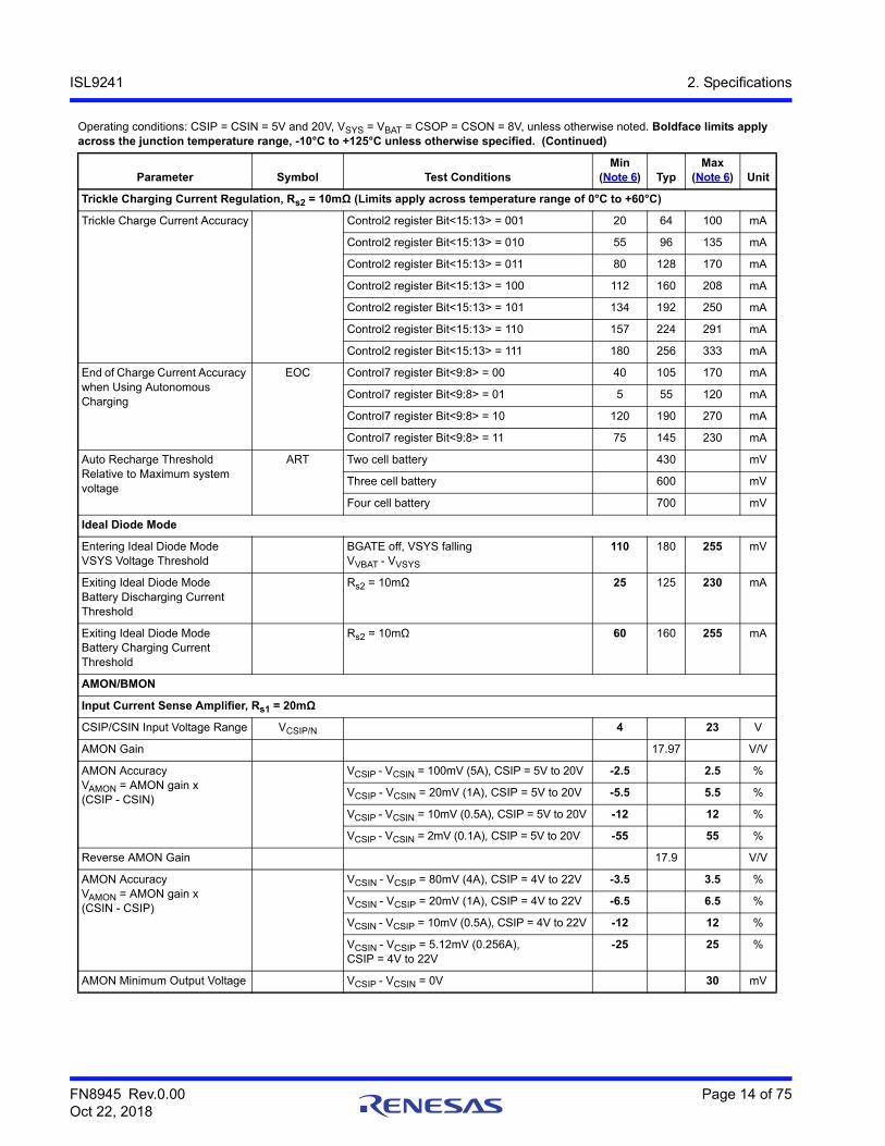
ISL9241 2. Specifications
Trickle Charging Current Regulation, Rs2 = 10mΩ (Limits apply across temperature range of 0°C to +60°C)
Trickle Charge Current Accuracy Control2 register Bit<15:13> = 001 20 64 100 mA
Control2 register Bit<15:13> = 010 55 96 135 mA
Control2 register Bit<15:13> = 011 80 128 170 mA
Control2 register Bit<15:13> = 100 112 160 208 mA
Control2 register Bit<15:13> = 101 134 192 250 mA
Control2 register Bit<15:13> = 110 157 224 291 mA
Control2 register Bit<15:13> = 111 180 256 333 mA
End of Charge Current Accuracy when Using Autonomous Charging
EOC Control7 register Bit<9:8> = 00 40 105 170 mA
Control7 register Bit<9:8> = 01 5 55 120 mA
Control7 register Bit<9:8> = 10 120 190 270 mA
Control7 register Bit<9:8> = 11 75 145 230 mA
Auto Recharge ThresholdRelative to Maximum system voltage
ART Two cell battery 430 mV
Three cell battery 600 mV
Four cell battery 700 mV
Ideal Diode Mode
Entering Ideal Diode Mode VSYS Voltage Threshold
BGATE off, VSYS fallingVVBAT - VVSYS
110 180 255 mV
Exiting Ideal Diode Mode Battery Discharging Current Threshold
Rs2 = 10mΩ 25 125 230 mA
Exiting Ideal Diode Mode Battery Charging Current Threshold
Rs2 = 10mΩ 60 160 255 mA
AMON/BMON
Input Current Sense Amplifier, Rs1 = 20mΩ
CSIP/CSIN Input Voltage Range VCSIP/N 4 23 V
AMON Gain 17.97 V/V
AMON AccuracyVAMON = AMON gain x (CSIP - CSIN)
VCSIP - VCSIN = 100mV (5A), CSIP = 5V to 20V -2.5 2.5 %
VCSIP - VCSIN = 20mV (1A), CSIP = 5V to 20V -5.5 5.5 %
VCSIP - VCSIN = 10mV (0.5A), CSIP = 5V to 20V -12 12 %
VCSIP - VCSIN = 2mV (0.1A), CSIP = 5V to 20V -55 55 %
Reverse AMON Gain 17.9 V/V
AMON AccuracyVAMON = AMON gain x (CSIN - CSIP)
VCSIN - VCSIP = 80mV (4A), CSIP = 4V to 22V -3.5 3.5 %
VCSIN - VCSIP = 20mV (1A), CSIP = 4V to 22V -6.5 6.5 %
VCSIN - VCSIP = 10mV (0.5A), CSIP = 4V to 22V -12 12 %
VCSIN - VCSIP = 5.12mV (0.256A), CSIP = 4V to 22V
-25 25 %
AMON Minimum Output Voltage VCSIP - VCSIN = 0V 30 mV
Operating conditions: CSIP = CSIN = 5V and 20V, VSYS = VBAT = CSOP = CSON = 8V, unless otherwise noted. Boldface limits apply across the junction temperature range, -10°C to +125°C unless otherwise specified. (Continued)
Parameter Symbol Test ConditionsMin
(Note 6) TypMax
(Note 6) Unit
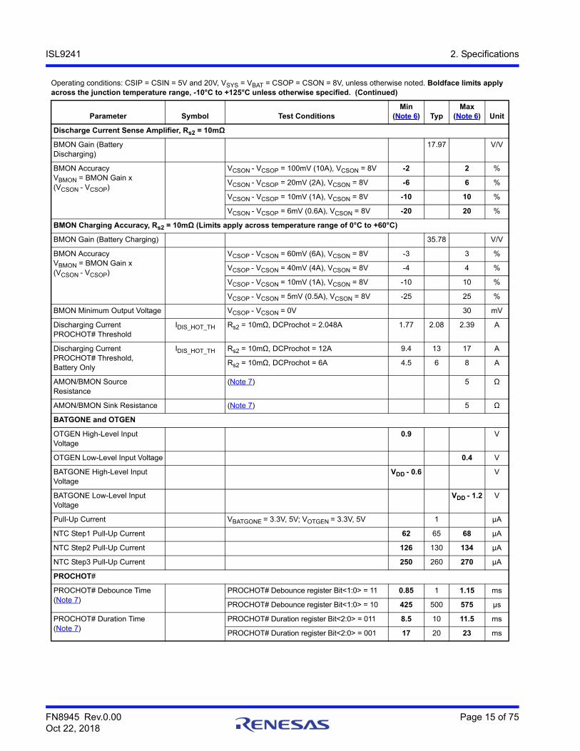
FN8945 Rev.0.00 Page 15 of 75Oct 22, 2018
ISL9241 2. Specifications
Discharge Current Sense Amplifier, Rs2 = 10mΩ
BMON Gain (Battery Discharging)
17.97 V/V
BMON AccuracyVBMON = BMON Gain x (VCSON - VCSOP)
VCSON - VCSOP = 100mV (10A), VCSON = 8V -2 2 %
VCSON - VCSOP = 20mV (2A), VCSON = 8V -6 6 %
VCSON - VCSOP = 10mV (1A), VCSON = 8V -10 10 %
VCSON - VCSOP = 6mV (0.6A), VCSON = 8V -20 20 %
BMON Charging Accuracy, Rs2 = 10mΩ (Limits apply across temperature range of 0°C to +60°C)
BMON Gain (Battery Charging) 35.78 V/V
BMON AccuracyVBMON = BMON Gain x (VCSON - VCSOP)
VCSOP - VCSON = 60mV (6A), VCSON = 8V -3 3 %
VCSOP - VCSON = 40mV (4A), VCSON = 8V -4 4 %
VCSOP - VCSON = 10mV (1A), VCSON = 8V -10 10 %
VCSOP - VCSON = 5mV (0.5A), VCSON = 8V -25 25 %
BMON Minimum Output Voltage VCSOP - VCSON = 0V 30 mV
Discharging Current PROCHOT# Threshold
IDIS_HOT_TH Rs2 = 10mΩ, DCProchot = 2.048A 1.77 2.08 2.39 A
Discharging Current PROCHOT# Threshold,Battery Only
IDIS_HOT_TH Rs2 = 10mΩ, DCProchot = 12A 9.4 13 17 A
Rs2 = 10mΩ, DCProchot = 6A 4.5 6 8 A
AMON/BMON Source Resistance
(Note 7) 5 Ω
AMON/BMON Sink Resistance (Note 7) 5 Ω
BATGONE and OTGEN
OTGEN High-Level Input Voltage
0.9 V
OTGEN Low-Level Input Voltage 0.4 V
BATGONE High-Level Input Voltage
VDD - 0.6 V
BATGONE Low-Level Input Voltage
VDD - 1.2 V
Pull-Up Current VBATGONE = 3.3V, 5V; VOTGEN = 3.3V, 5V 1 µA
NTC Step1 Pull-Up Current 62 65 68 µA
NTC Step2 Pull-Up Current 126 130 134 µA
NTC Step3 Pull-Up Current 250 260 270 µA
PROCHOT#
PROCHOT# Debounce Time(Note 7)
PROCHOT# Debounce register Bit<1:0> = 11 0.85 1 1.15 ms
PROCHOT# Debounce register Bit<1:0> = 10 425 500 575 µs
PROCHOT# Duration Time(Note 7)
PROCHOT# Duration register Bit<2:0> = 011 8.5 10 11.5 ms
PROCHOT# Duration register Bit<2:0> = 001 17 20 23 ms
Operating conditions: CSIP = CSIN = 5V and 20V, VSYS = VBAT = CSOP = CSON = 8V, unless otherwise noted. Boldface limits apply across the junction temperature range, -10°C to +125°C unless otherwise specified. (Continued)
Parameter Symbol Test ConditionsMin
(Note 6) TypMax
(Note 6) Unit
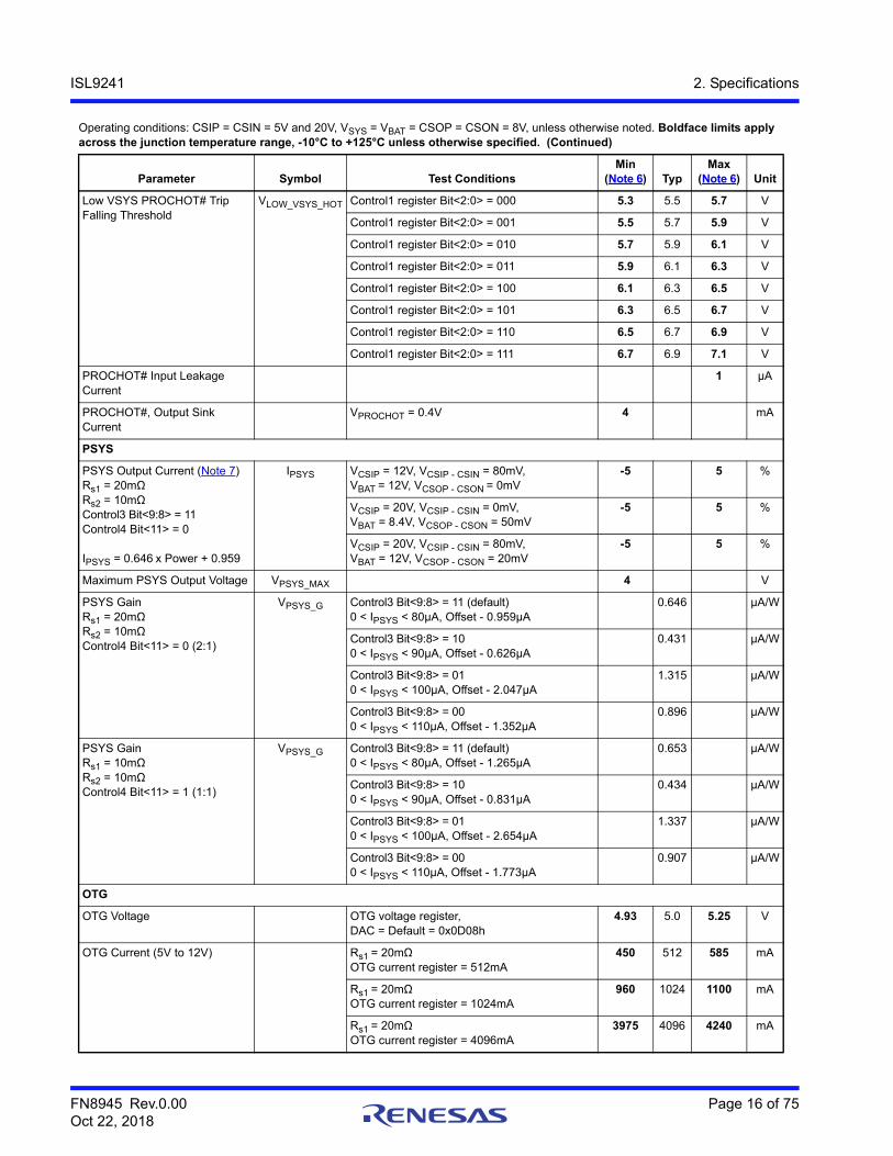
FN8945 Rev.0.00 Page 16 of 75Oct 22, 2018
ISL9241 2. Specifications
Low VSYS PROCHOT# Trip Falling Threshold
VLOW_VSYS_HOT Control1 register Bit<2:0> = 000 5.3 5.5 5.7 V
Control1 register Bit<2:0> = 001 5.5 5.7 5.9 V
Control1 register Bit<2:0> = 010 5.7 5.9 6.1 V
Control1 register Bit<2:0> = 011 5.9 6.1 6.3 V
Control1 register Bit<2:0> = 100 6.1 6.3 6.5 V
Control1 register Bit<2:0> = 101 6.3 6.5 6.7 V
Control1 register Bit<2:0> = 110 6.5 6.7 6.9 V
Control1 register Bit<2:0> = 111 6.7 6.9 7.1 V
PROCHOT# Input Leakage Current
1 µA
PROCHOT#, Output Sink Current
VPROCHOT = 0.4V 4 mA
PSYS
PSYS Output Current (Note 7)Rs1 = 20mΩRs2 = 10mΩControl3 Bit<9:8> = 11Control4 Bit<11> = 0
IPSYS = 0.646 x Power + 0.959
IPSYS VCSIP = 12V, VCSIP - CSIN = 80mV,VBAT = 12V, VCSOP - CSON = 0mV
-5 5 %
VCSIP = 20V, VCSIP - CSIN = 0mV,VBAT = 8.4V, VCSOP - CSON = 50mV
-5 5 %
VCSIP = 20V, VCSIP - CSIN = 80mV,VBAT = 12V, VCSOP - CSON = 20mV
-5 5 %
Maximum PSYS Output Voltage VPSYS_MAX 4 V
PSYS GainRs1 = 20mΩRs2 = 10mΩControl4 Bit<11> = 0 (2:1)
VPSYS_G Control3 Bit<9:8> = 11 (default)0 < IPSYS < 80µA, Offset - 0.959µA
0.646 µA/W
Control3 Bit<9:8> = 100 < IPSYS < 90µA, Offset - 0.626µA
0.431 µA/W
Control3 Bit<9:8> = 010 < IPSYS < 100µA, Offset - 2.047µA
1.315 µA/W
Control3 Bit<9:8> = 000 < IPSYS < 110µA, Offset - 1.352µA
0.896 µA/W
PSYS GainRs1 = 10mΩRs2 = 10mΩControl4 Bit<11> = 1 (1:1)
VPSYS_G Control3 Bit<9:8> = 11 (default)0 < IPSYS < 80µA, Offset - 1.265µA
0.653 µA/W
Control3 Bit<9:8> = 100 < IPSYS < 90µA, Offset - 0.831µA
0.434 µA/W
Control3 Bit<9:8> = 010 < IPSYS < 100µA, Offset - 2.654µA
1.337 µA/W
Control3 Bit<9:8> = 000 < IPSYS < 110µA, Offset - 1.773µA
0.907 µA/W
OTG
OTG Voltage OTG voltage register, DAC = Default = 0x0D08h
4.93 5.0 5.25 V
OTG Current (5V to 12V) Rs1 = 20mΩOTG current register = 512mA
450 512 585 mA
Rs1 = 20mΩOTG current register = 1024mA
960 1024 1100 mA
Rs1 = 20mΩOTG current register = 4096mA
3975 4096 4240 mA
Operating conditions: CSIP = CSIN = 5V and 20V, VSYS = VBAT = CSOP = CSON = 8V, unless otherwise noted. Boldface limits apply across the junction temperature range, -10°C to +125°C unless otherwise specified. (Continued)
Parameter Symbol Test ConditionsMin
(Note 6) TypMax
(Note 6) Unit
FN8945 Rev.0.00 Page 17 of 75Oct 22, 2018
ISL9241 2. Specifications
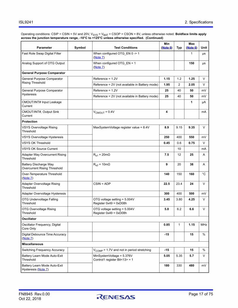
Fast Role Swap Digital Filter When configured OTG_EN 0 -> 1(Note 7)
1 µs
Analog Support of OTG Output When configured OTG_EN = 1(Note 7)
150 µs
General Purpose Comparator
General Purpose Comparator Rising Threshold
Reference = 1.2V 1.15 1.2 1.25 V
Reference = 2V (not available in Battery mode) 1.95 2 2.05 V
General Purpose Comparator Hysteresis
Reference = 1.2V 25 40 50 mV
Reference = 2V (not available in Battery mode) 25 40 50 mV
CMOUT/INT# Input Leakage Current
1 µA
CMOUT/INT#, Output Sink Current
VCMOUT = 0.4V 4 mA
Protection
VSYS Overvoltage Rising Threshold
MaxSystemVoltage register value = 8.4V 8.9 9.15 9.35 V
VSYS Overvoltage Hysteresis 250 400 550 mV
VSYS OK Threshold 0.45 0.6 0.75 V
VSYS OK Source Current 10 mA
Adapter Way Overcurrent Rising Threshold
Rs1 = 20mΩ 7.5 12 25 A
Battery Discharge Way Overcurrent Rising Threshold
Rs2 = 10mΩ 9 20 38 A
Over-Temperature Threshold (Note 7)
140 150 160 °C
Adapter Overvoltage Rising Threshold
CSIN = ADP 22.5 23.4 24 V
Adapter Overvoltage Hysteresis 300 400 500 mV
OTG Undervoltage Falling Threshold
OTG voltage setting = 5.004VRegister 0x49 = 0xD08h
3.45 3.80 4.25 V
OTG Overvoltage Rising Threshold
OTG voltage setting = 5.004VRegister 0x49 = 0xD08h
5.8 6.2 6.6 V
Oscillator
Oscillator Frequency, Digital Core Only
0.85 1 1.15 MHz
Digital Debounce Time Accuracy (Note 7)
-15 15 %
Miscellaneous
Switching Frequency Accuracy VCOMP > 1.7V and not in period stretching -15 15 %
Battery Learn Mode Auto-Exit Threshold
MinSystemVoltage = 5.376VControl1 register Bit<13> = 1
5.05 5.35 5.7 V
Battery Learn Mode Auto-Exit Hysteresis (Note 7)
180 330 480 mV
Operating conditions: CSIP = CSIN = 5V and 20V, VSYS = VBAT = CSOP = CSON = 8V, unless otherwise noted. Boldface limits apply across the junction temperature range, -10°C to +125°C unless otherwise specified. (Continued)
Parameter Symbol Test ConditionsMin
(Note 6) TypMax
(Note 6) Unit
FN8945 Rev.0.00 Page 18 of 75Oct 22, 2018
ISL9241 2. Specifications
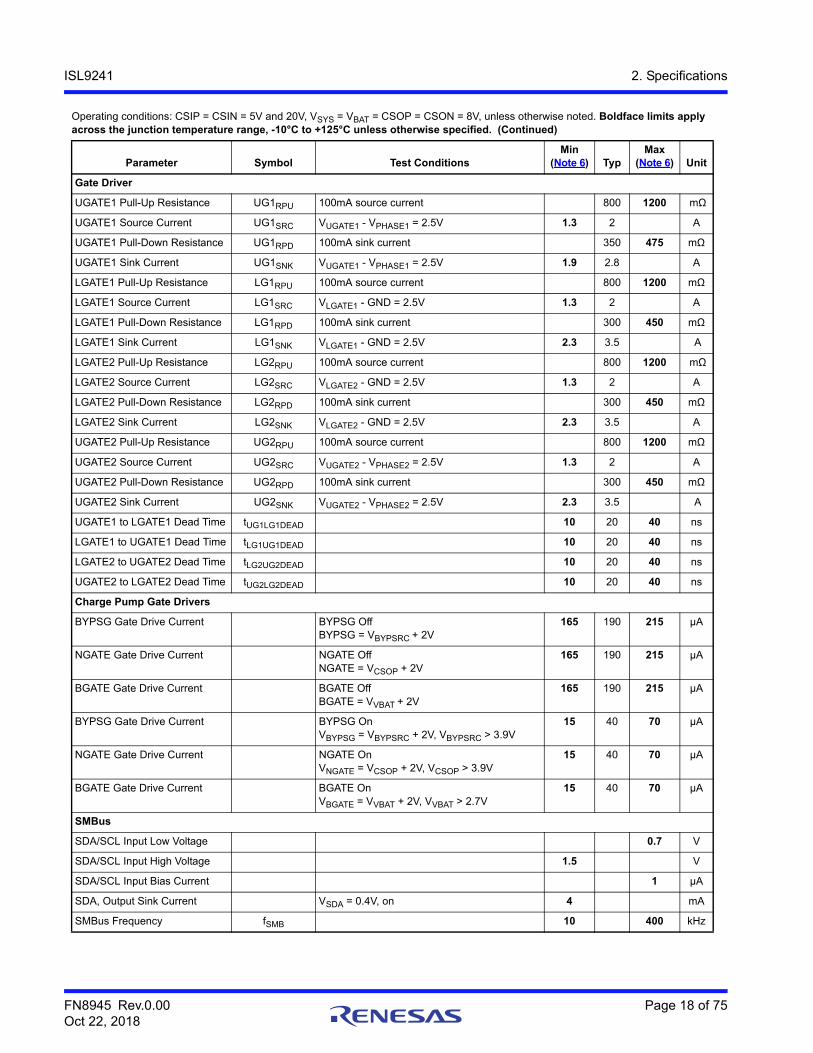
Gate Driver
UGATE1 Pull-Up Resistance UG1RPU 100mA source current 800 1200 mΩ
UGATE1 Source Current UG1SRC VUGATE1 - VPHASE1 = 2.5V 1.3 2 A
UGATE1 Pull-Down Resistance UG1RPD 100mA sink current 350 475 mΩ
UGATE1 Sink Current UG1SNK VUGATE1 - VPHASE1 = 2.5V 1.9 2.8 A
LGATE1 Pull-Up Resistance LG1RPU 100mA source current 800 1200 mΩ
LGATE1 Source Current LG1SRC VLGATE1 - GND = 2.5V 1.3 2 A
LGATE1 Pull-Down Resistance LG1RPD 100mA sink current 300 450 mΩ
LGATE1 Sink Current LG1SNK VLGATE1 - GND = 2.5V 2.3 3.5 A
LGATE2 Pull-Up Resistance LG2RPU 100mA source current 800 1200 mΩ
LGATE2 Source Current LG2SRC VLGATE2 - GND = 2.5V 1.3 2 A
LGATE2 Pull-Down Resistance LG2RPD 100mA sink current 300 450 mΩ
LGATE2 Sink Current LG2SNK VLGATE2 - GND = 2.5V 2.3 3.5 A
UGATE2 Pull-Up Resistance UG2RPU 100mA source current 800 1200 mΩ
UGATE2 Source Current UG2SRC VUGATE2 - VPHASE2 = 2.5V 1.3 2 A
UGATE2 Pull-Down Resistance UG2RPD 100mA sink current 300 450 mΩ
UGATE2 Sink Current UG2SNK VUGATE2 - VPHASE2 = 2.5V 2.3 3.5 A
UGATE1 to LGATE1 Dead Time tUG1LG1DEAD 10 20 40 ns
LGATE1 to UGATE1 Dead Time tLG1UG1DEAD 10 20 40 ns
LGATE2 to UGATE2 Dead Time tLG2UG2DEAD 10 20 40 ns
UGATE2 to LGATE2 Dead Time tUG2LG2DEAD 10 20 40 ns
Charge Pump Gate Drivers
BYPSG Gate Drive Current BYPSG OffBYPSG = VBYPSRC + 2V
165 190 215 µA
NGATE Gate Drive Current NGATE OffNGATE = VCSOP + 2V
165 190 215 µA
BGATE Gate Drive Current BGATE OffBGATE = VVBAT + 2V
165 190 215 µA
BYPSG Gate Drive Current BYPSG OnVBYPSG = VBYPSRC + 2V, VBYPSRC > 3.9V
15 40 70 µA
NGATE Gate Drive Current NGATE OnVNGATE = VCSOP + 2V, VCSOP > 3.9V
15 40 70 µA
BGATE Gate Drive Current BGATE OnVBGATE = VVBAT + 2V, VVBAT > 2.7V
15 40 70 µA
SMBus
SDA/SCL Input Low Voltage 0.7 V
SDA/SCL Input High Voltage 1.5 V
SDA/SCL Input Bias Current 1 µA
SDA, Output Sink Current VSDA = 0.4V, on 4 mA
SMBus Frequency fSMB 10 400 kHz
Operating conditions: CSIP = CSIN = 5V and 20V, VSYS = VBAT = CSOP = CSON = 8V, unless otherwise noted. Boldface limits apply across the junction temperature range, -10°C to +125°C unless otherwise specified. (Continued)
Parameter Symbol Test ConditionsMin
(Note 6) TypMax
(Note 6) Unit
FN8945 Rev.0.00 Page 19 of 75Oct 22, 2018
ISL9241 2. Specifications
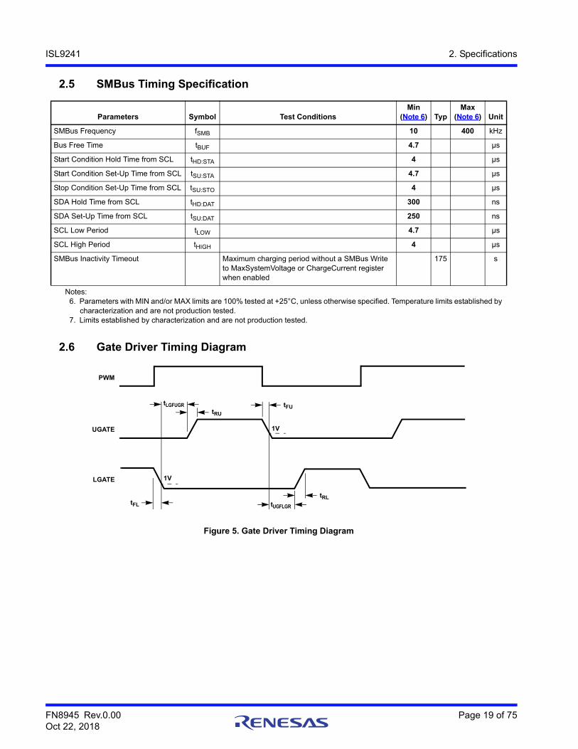
2.5 SMBus Timing Specification
2.6 Gate Driver Timing Diagram
Figure 5. Gate Driver Timing Diagram
Parameters Symbol Test ConditionsMin
(Note 6) TypMax
(Note 6) Unit
SMBus Frequency fSMB 10 400 kHz
Bus Free Time tBUF 4.7 µs
Start Condition Hold Time from SCL tHD:STA 4 µs
Start Condition Set-Up Time from SCL tSU:STA 4.7 µs
Stop Condition Set-Up Time from SCL tSU:STO 4 µs
SDA Hold Time from SCL tHD:DAT 300 ns
SDA Set-Up Time from SCL tSU:DAT 250 ns
SCL Low Period tLOW 4.7 µs
SCL High Period tHIGH 4 µs
SMBus Inactivity Timeout Maximum charging period without a SMBus Write to MaxSystemVoltage or ChargeCurrent register when enabled
175 s
Notes:6. Parameters with MIN and/or MAX limits are 100% tested at +25°C, unless otherwise specified. Temperature limits established by
characterization and are not production tested.7. Limits established by characterization and are not production tested.
PWM
UGATE
LGATE 1V
1V
tUGFLGR
tRL
tFUtRU
tFL
tLGFUGR
FN8945 Rev.0.00 Page 20 of 75Oct 22, 2018
ISL9241 3. Typical Performance
3. Typical Performance
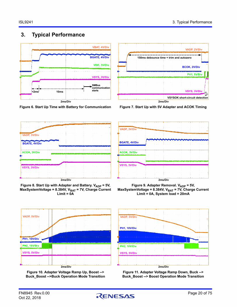
Figure 6. Start Up Time with Battery for Communication Figure 7. Start Up with 5V Adapter and ACOK Timing
Figure 8. Start Up with Adapter and Battery. VADP = 5V, MaxSystemVoltage = 8.384V, VBAT = 7V, Charge Current
Limit = 0A
Figure 9. Adapter Removal. VADP = 5V, MaxSystemVoltage = 8.384V, VBAT = 7V, Charge Current
Limit = 0A, System load = 20mA
Figure 10. Adapter Voltage Ramp Up, Boost --> Buck_Boost -->Buck Operation Mode Transition
Figure 11. Adapter Voltage Ramp Down, Buck --> Buck_Boost --> Boost Operation Mode Transition
VBAT, 4V/Div
BGATE, 4V/Div
VDD, 3V/Div
VSYS, 3V/Div
2ms/Div
<2ms 10ms
SMBuscommunicationstarts
VADP, 2V/Div
BCOK, 2V/Div
PH1, 5V/Div
VSYS, 3V/Div
150ms debounce time + trim and autozero
VSYSOK short-circuit detection
2ms/Div
VADP, 3V/Div
BGATE, 4V/Div
ACOK, 3V/Div
VSYS, 3V/Div
2ms/Div
VADP, 2V/Div
BCOK, 2V/Div
PH1, 5V/Div
VSYS, 3V/Div
2ms/Div
VADP, 3V/Div
BGATE, 4V/Div
ACOK, 3V/Div
VSYS, 3V/Div
2ms/Div
VADP, 5V/Div
PH1, 10V/Div
PH2, 10V/Div
VSYS, 5V/Div
2ms/Div
VADP, 5V/Div
PH1, 10V/Div
PH2, 10V/Div
VSYS, 5V/Div
2ms/Div
FN8945 Rev.0.00 Page 21 of 75Oct 22, 2018
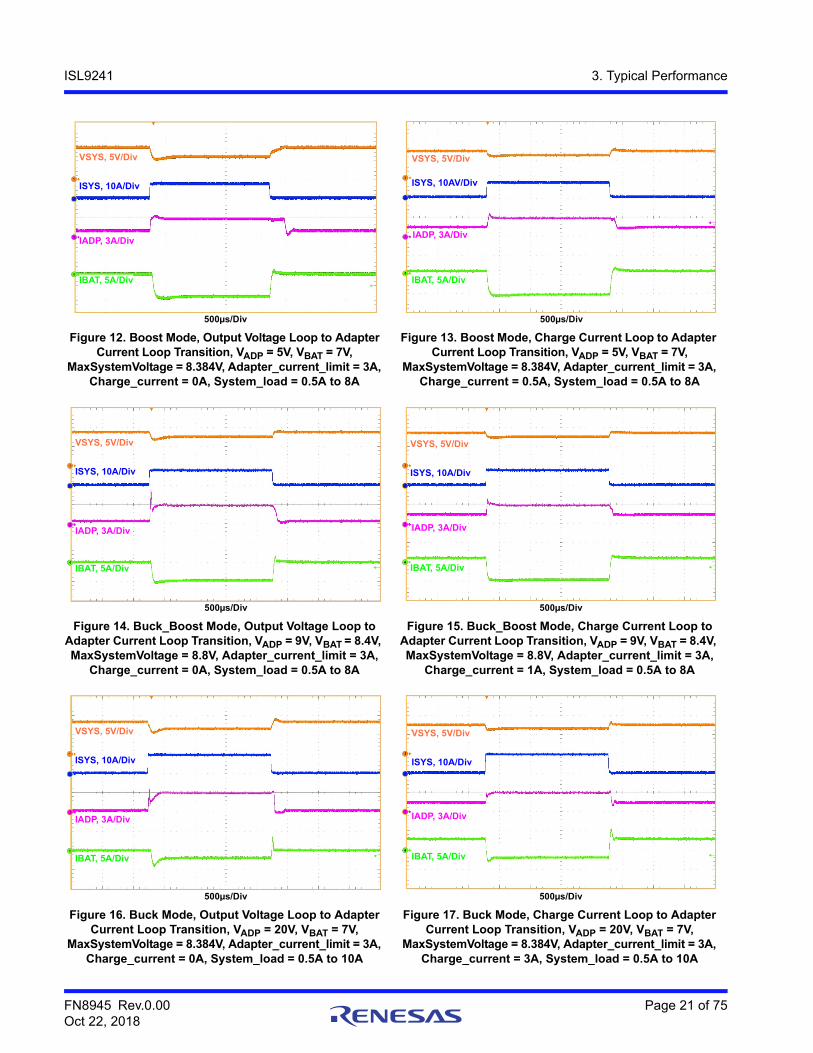
ISL9241 3. Typical Performance
Figure 12. Boost Mode, Output Voltage Loop to Adapter Current Loop Transition, VADP = 5V, VBAT = 7V,
MaxSystemVoltage = 8.384V, Adapter_current_limit = 3A, Charge_current = 0A, System_load = 0.5A to 8A
Figure 13. Boost Mode, Charge Current Loop to Adapter Current Loop Transition, VADP = 5V, VBAT = 7V,
MaxSystemVoltage = 8.384V, Adapter_current_limit = 3A, Charge_current = 0.5A, System_load = 0.5A to 8A
Figure 14. Buck_Boost Mode, Output Voltage Loop to Adapter Current Loop Transition, VADP = 9V, VBAT = 8.4V, MaxSystemVoltage = 8.8V, Adapter_current_limit = 3A,
Charge_current = 0A, System_load = 0.5A to 8A
Figure 15. Buck_Boost Mode, Charge Current Loop to Adapter Current Loop Transition, VADP = 9V, VBAT = 8.4V, MaxSystemVoltage = 8.8V, Adapter_current_limit = 3A,
Charge_current = 1A, System_load = 0.5A to 8A
Figure 16. Buck Mode, Output Voltage Loop to Adapter Current Loop Transition, VADP = 20V, VBAT = 7V,
MaxSystemVoltage = 8.384V, Adapter_current_limit = 3A, Charge_current = 0A, System_load = 0.5A to 10A
Figure 17. Buck Mode, Charge Current Loop to Adapter Current Loop Transition, VADP = 20V, VBAT = 7V,
MaxSystemVoltage = 8.384V, Adapter_current_limit = 3A, Charge_current = 3A, System_load = 0.5A to 10A
VSYS, 5V/Div
ISYS, 10A/Div
IBAT, 5A/Div
IADP, 3A/Div
500µs/Div
VSYS, 5V/Div
ISYS, 10AV/Div
IBAT, 5A/Div
IADP, 3A/Div
500µs/Div
VSYS, 5V/Div
ISYS, 10A/Div
IBAT, 5A/Div
IADP, 3A/Div
500µs/Div
VSYS, 5V/Div
ISYS, 10A/Div
IBAT, 5A/Div
IADP, 3A/Div
500µs/Div
VSYS, 5V/Div
ISYS, 10A/Div
IBAT, 5A/Div
IADP, 3A/Div
500µs/Div
VSYS, 5V/Div
ISYS, 10A/Div
IBAT, 5A/Div
500µs/Div
IADP, 3A/Div
FN8945 Rev.0.00 Page 22 of 75Oct 22, 2018
ISL9241 3. Typical Performance
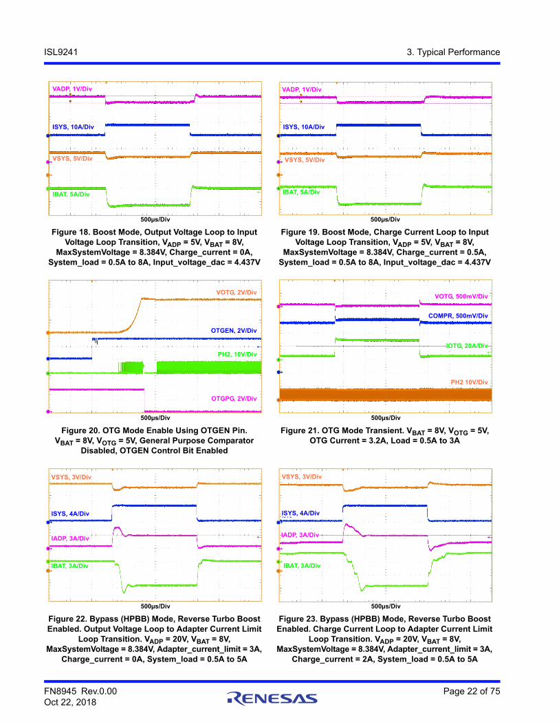
Figure 18. Boost Mode, Output Voltage Loop to Input Voltage Loop Transition, VADP = 5V, VBAT = 8V,
MaxSystemVoltage = 8.384V, Charge_current = 0A, System_load = 0.5A to 8A, Input_voltage_dac = 4.437V
Figure 19. Boost Mode, Charge Current Loop to Input Voltage Loop Transition, VADP = 5V, VBAT = 8V,
MaxSystemVoltage = 8.384V, Charge_current = 0.5A, System_load = 0.5A to 8A, Input_voltage_dac = 4.437V
Figure 20. OTG Mode Enable Using OTGEN Pin. VBAT = 8V, VOTG = 5V, General Purpose Comparator
Disabled, OTGEN Control Bit Enabled
Figure 21. OTG Mode Transient. VBAT = 8V, VOTG = 5V, OTG Current = 3.2A, Load = 0.5A to 3A
Figure 22. Bypass (HPBB) Mode, Reverse Turbo Boost Enabled. Output Voltage Loop to Adapter Current Limit
Loop Transition. VADP = 20V, VBAT = 8V, MaxSystemVoltage = 8.384V, Adapter_current_limit = 3A,
Charge_current = 0A, System_load = 0.5A to 5A
Figure 23. Bypass (HPBB) Mode, Reverse Turbo Boost Enabled. Charge Current Loop to Adapter Current Limit
Loop Transition. VADP = 20V, VBAT = 8V, MaxSystemVoltage = 8.384V, Adapter_current_limit = 3A,
Charge_current = 2A, System_load = 0.5A to 5A
VSYS, 5V/Div
ISYS, 10A/Div
IBAT, 5A/Div
500µs/Div
VADP, 1V/Div
VSYS, 5V/Div
ISYS, 10A/Div
IBAT, 5A/Div
500µs/Div
VADP, 1V/Div
VOTG, 2V/Div
OTGEN, 2V/Div
PH2, 10V/Div
500µs/Div
OTGPG, 2V/Div
PH2 10V/Div
COMPR, 500mV/Div
IOTG, 20A/Div
500µs/Div
VOTG, 500mV/Div
VSYS, 3V/Div
ISYS, 4A/Div
IBAT, 3A/Div
500µs/Div
IADP, 3A/Div
VSYS, 3V/Div
ISYS, 4A/Div
IBAT, 3A/Div
500µs/Div
IADP, 3A/Div
FN8945 Rev.0.00 Page 23 of 75Oct 22, 2018
ISL9241 3. Typical Performance
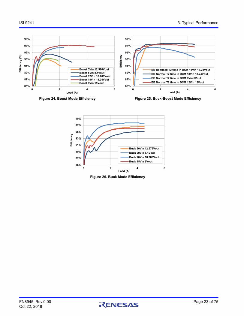
Figure 24. Boost Mode Efficiency Figure 25. Buck-Boost Mode Efficiency
Figure 26. Buck Mode Efficiency
85%
87%
89%
91%
93%
95%
97%
99%
0 2 4 6
Eff
icie
nc
y (
%)
Load (A)
Boost 5Vin 12.576Vout
Boost 5Vin 8.4Vout
Boost 12Vin 16.768Vout
Boost 15Vin 18.24Vout
Boost 6Vin 15Vout85%
87%
89%
91%
93%
95%
97%
99%
0 2 4 6
Eff
icie
nc
y
Load (A)
BB Reduced T2 time in DCM 18Vin 18.24Vout
BB Normal T2 time in DCM 18Vin 18.24Vout
BB Normal T2 time in DCM 6Vin 6Vout
BB Normal T2 time in DCM 12Vin 12Vout
85%
87%
89%
91%
93%
95%
97%
99%
0 2 4 6
Eff
icie
nc
y
Load (A)
Buck 20Vin 12.576Vout
Buck 20Vin 8.4Vout
Buck 20Vin 16.768Vout
Buck 15Vin 9Vout
FN8945 Rev.0.00 Page 24 of 75Oct 22, 2018
ISL9241 4. General SMBus Architecture
4. General SMBus Architecture
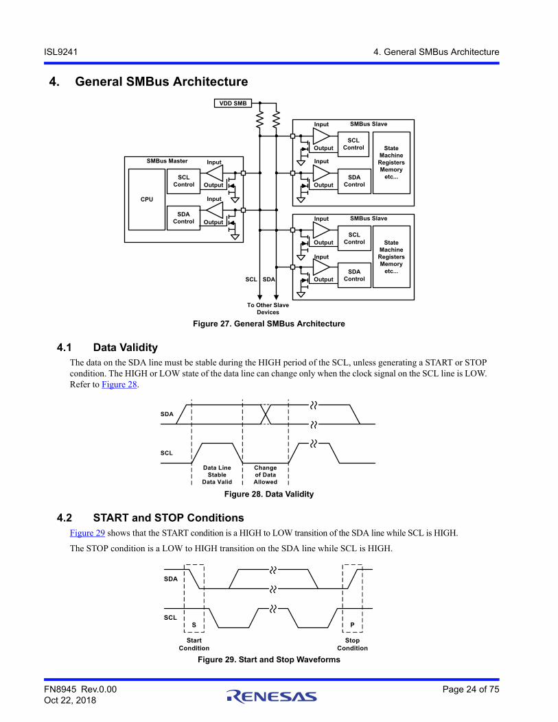
Figure 27. General SMBus Architecture
4.1 Data ValidityThe data on the SDA line must be stable during the HIGH period of the SCL, unless generating a START or STOP condition. The HIGH or LOW state of the data line can change only when the clock signal on the SCL line is LOW. Refer to Figure 28.
Figure 28. Data Validity
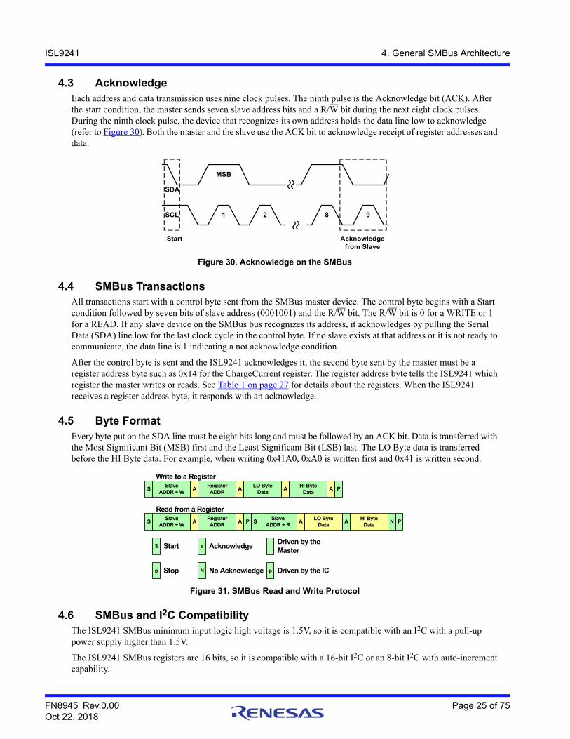
4.2 START and STOP ConditionsFigure 29 shows that the START condition is a HIGH to LOW transition of the SDA line while SCL is HIGH.
The STOP condition is a LOW to HIGH transition on the SDA line while SCL is HIGH.
Figure 29. Start and Stop Waveforms
SDA
SCL
Data LineStable
Data Valid
Changeof DataAllowed
SDA
SCLS
StartCondition
P
StopCondition
FN8945 Rev.0.00 Page 25 of 75Oct 22, 2018
ISL9241 4. General SMBus Architecture
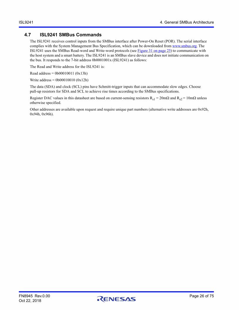
4.3 AcknowledgeEach address and data transmission uses nine clock pulses. The ninth pulse is the Acknowledge bit (ACK). After the start condition, the master sends seven slave address bits and a R/W bit during the next eight clock pulses. During the ninth clock pulse, the device that recognizes its own address holds the data line low to acknowledge (refer to Figure 30). Both the master and the slave use the ACK bit to acknowledge receipt of register addresses and data.
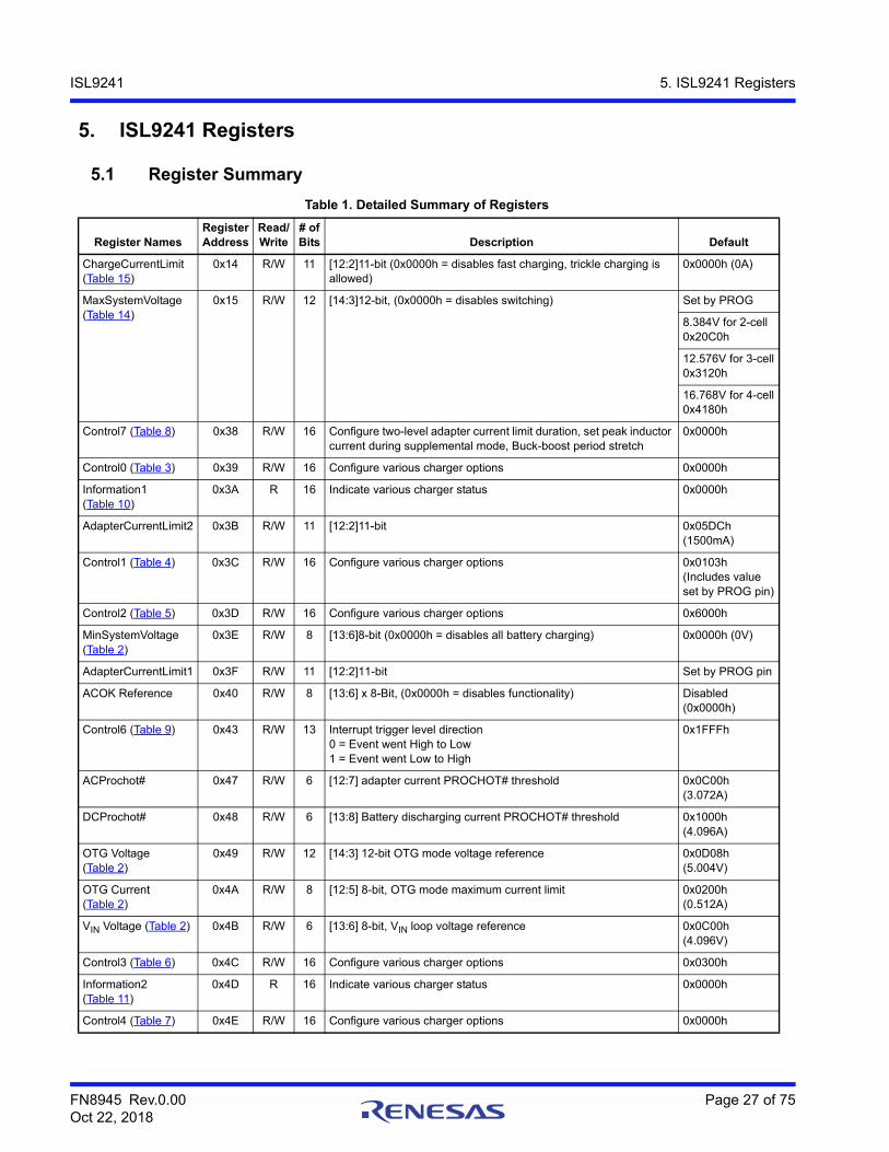
4.4 SMBus TransactionsAll transactions start with a control byte sent from the SMBus master device. The control byte begins with a Start condition followed by seven bits of slave address (0001001) and the R/W bit. The R/W bit is 0 for a WRITE or 1 for a READ. If any slave device on the SMBus bus recognizes its address, it acknowledges by pulling the Serial Data (SDA) line low for the last clock cycle in the control byte. If no slave exists at that address or it is not ready to communicate, the data line is 1 indicating a not acknowledge condition.
After the control byte is sent and the ISL9241 acknowledges it, the second byte sent by the master must be a register address byte such as 0x14 for the ChargeCurrent register. The register address byte tells the ISL9241 which register the master writes or reads. See Table 1 on page 27 for details about the registers. When the ISL9241 receives a register address byte, it responds with an acknowledge.
4.5 Byte FormatEvery byte put on the SDA line must be eight bits long and must be followed by an ACK bit. Data is transferred with the Most Significant Bit (MSB) first and the Least Significant Bit (LSB) last. The LO Byte data is transferred before the HI Byte data. For example, when writing 0x41A0, 0xA0 is written first and 0x41 is written second.
Figure 31. SMBus Read and Write Protocol
4.6 SMBus and I2C CompatibilityThe ISL9241 SMBus minimum input logic high voltage is 1.5V, so it is compatible with an I2C with a pull-up power supply higher than 1.5V.
The ISL9241 SMBus registers are 16 bits, so it is compatible with a 16-bit I2C or an 8-bit I2C with auto-increment capability.
Figure 30. Acknowledge on the SMBus
SDA
SCL
Start Acknowledgefrom Slave
1 2 8 9
MSB
SSlave
ADDR + WA
RegisterADDR
ALO Byte
DataA
HI Byte Data
A P
Write to a Register
SSlave
ADDR + WA
RegisterADDR
A
Read from a Register
P SSlave
ADDR + RA
LO Byte Data
AHI Byte
DataN P
S Start
p Stop
a Acknowledge
N No Acknowledge
Driven by the Master
p Driven by the IC
FN8945 Rev.0.00 Page 26 of 75Oct 22, 2018
ISL9241 4. General SMBus Architecture
4.7 ISL9241 SMBus CommandsThe ISL9241 receives control inputs from the SMBus interface after Power-On Reset (POR). The serial interface complies with the System Management Bus Specification, which can be downloaded from www.smbus.org. The ISL9241 uses the SMBus Read-word and Write-word protocols (see Figure 31 on page 25) to communicate with the host system and a smart battery. The ISL9241 is an SMBus slave device and does not initiate communication on the bus. It responds to the 7-bit address 0b0001001x (ISL9241) as follows:
The Read and Write address for the ISL9241 is:
Read address = 0b00010011 (0x13h)
Write address = 0b00010010 (0x12h)
The data (SDA) and clock (SCL) pins have Schmitt-trigger inputs that can accommodate slow edges. Choose pull-up resistors for SDA and SCL to achieve rise times according to the SMBus specifications.
Register DAC values in this datasheet are based on current-sensing resistors Rs1 = 20mΩand Rs2 = 10mΩ unless otherwise specified.
Other addresses are available upon request and require unique part numbers (alternative write addresses are 0x92h, 0x94h, 0x96h).
FN8945 Rev.0.00 Page 27 of 75Oct 22, 2018
ISL9241 5. ISL9241 Registers
5. ISL9241 Registers
5.1 Register Summary
Table 1. Detailed Summary of Registers
Register NamesRegisterAddress
Read/Write
# ofBits Description Default
ChargeCurrentLimit(Table 15)
0x14 R/W 11 [12:2]11-bit (0x0000h = disables fast charging, trickle charging is allowed)
0x0000h (0A)
MaxSystemVoltage(Table 14)
0x15 R/W 12 [14:3]12-bit, (0x0000h = disables switching) Set by PROG
8.384V for 2-cell0x20C0h
12.576V for 3-cell0x3120h
16.768V for 4-cell0x4180h
Control7 (Table 8) 0x38 R/W 16 Configure two-level adapter current limit duration, set peak inductor current during supplemental mode, Buck-boost period stretch
0x0000h
Control0 (Table 3) 0x39 R/W 16 Configure various charger options 0x0000h
Information1 (Table 10)
0x3A R 16 Indicate various charger status 0x0000h
AdapterCurrentLimit2 0x3B R/W 11 [12:2]11-bit 0x05DCh (1500mA)
Control1 (Table 4) 0x3C R/W 16 Configure various charger options 0x0103h (Includes value set by PROG pin)
Control2 (Table 5) 0x3D R/W 16 Configure various charger options 0x6000h
MinSystemVoltage(Table 2)
0x3E R/W 8 [13:6]8-bit (0x0000h = disables all battery charging) 0x0000h (0V)
AdapterCurrentLimit1 0x3F R/W 11 [12:2]11-bit Set by PROG pin
ACOK Reference 0x40 R/W 8 [13:6] x 8-Bit, (0x0000h = disables functionality) Disabled (0x0000h)
Control6 (Table 9) 0x43 R/W 13 Interrupt trigger level direction 0 = Event went High to Low1 = Event went Low to High
0x1FFFh
ACProchot# 0x47 R/W 6 [12:7] adapter current PROCHOT# threshold 0x0C00h (3.072A)
DCProchot# 0x48 R/W 6 [13:8] Battery discharging current PROCHOT# threshold 0x1000h(4.096A)
OTG Voltage (Table 2)
0x49 R/W 12 [14:3] 12-bit OTG mode voltage reference 0x0D08h (5.004V)
OTG Current (Table 2)
0x4A R/W 8 [12:5] 8-bit, OTG mode maximum current limit 0x0200h (0.512A)
VIN Voltage (Table 2) 0x4B R/W 6 [13:6] 8-bit, VIN loop voltage reference 0x0C00h (4.096V)
Control3 (Table 6) 0x4C R/W 16 Configure various charger options 0x0300h
Information2 (Table 11)
0x4D R 16 Indicate various charger status 0x0000h
Control4 (Table 7) 0x4E R/W 16 Configure various charger options 0x0000h
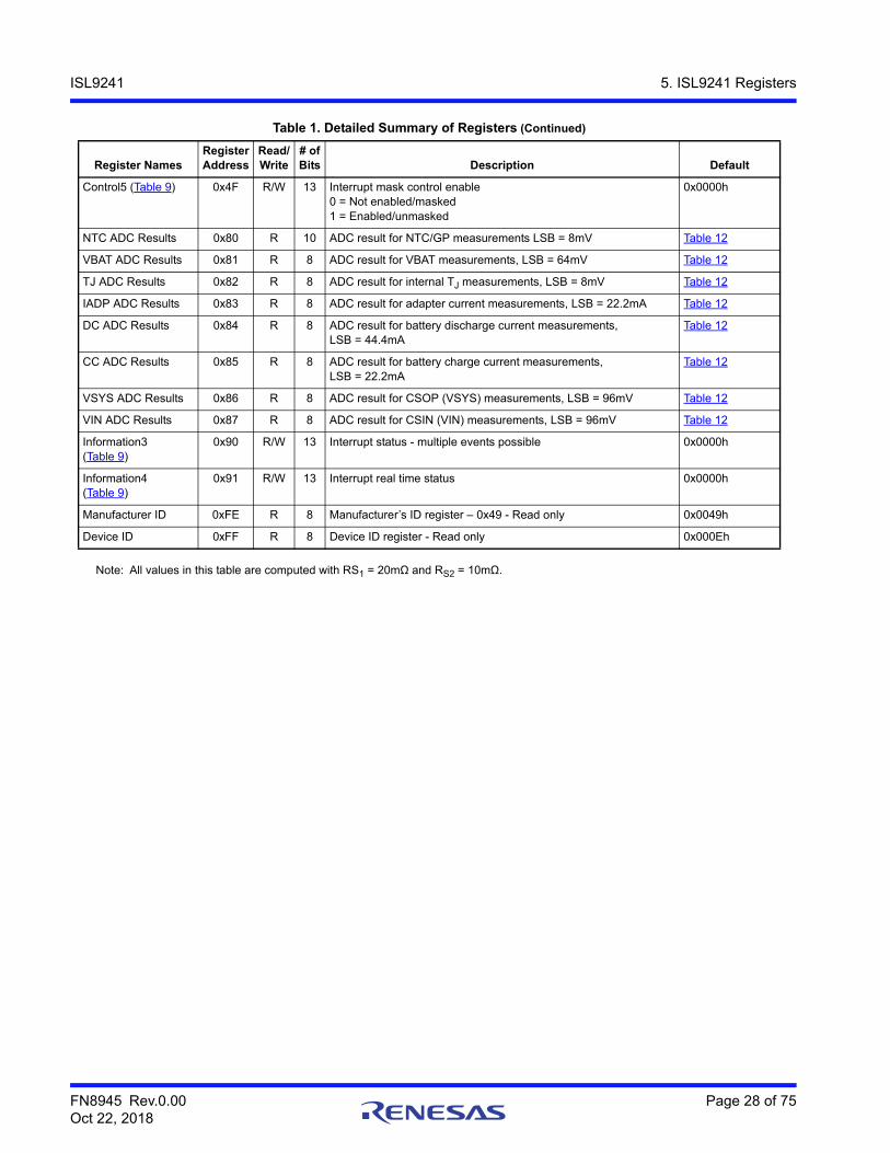
FN8945 Rev.0.00 Page 28 of 75Oct 22, 2018
ISL9241 5. ISL9241 Registers
Note: All values in this table are computed with RS1 = 20mΩ and RS2 = 10mΩ.
Control5 (Table 9) 0x4F R/W 13 Interrupt mask control enable0 = Not enabled/masked1 = Enabled/unmasked
0x0000h
NTC ADC Results 0x80 R 10 ADC result for NTC/GP measurements LSB = 8mV Table 12
VBAT ADC Results 0x81 R 8 ADC result for VBAT measurements, LSB = 64mV Table 12
TJ ADC Results 0x82 R 8 ADC result for internal TJ measurements, LSB = 8mV Table 12
IADP ADC Results 0x83 R 8 ADC result for adapter current measurements, LSB = 22.2mA Table 12
DC ADC Results 0x84 R 8 ADC result for battery discharge current measurements, LSB = 44.4mA
Table 12
CC ADC Results 0x85 R 8 ADC result for battery charge current measurements, LSB = 22.2mA
Table 12
VSYS ADC Results 0x86 R 8 ADC result for CSOP (VSYS) measurements, LSB = 96mV Table 12
VIN ADC Results 0x87 R 8 ADC result for CSIN (VIN) measurements, LSB = 96mV Table 12
Information3 (Table 9)
0x90 R/W 13 Interrupt status - multiple events possible 0x0000h
Information4 (Table 9)
0x91 R/W 13 Interrupt real time status 0x0000h
Manufacturer ID 0xFE R 8 Manufacturer’s ID register – 0x49 - Read only 0x0049h
Device ID 0xFF R 8 Device ID register - Read only 0x000Eh
Table 1. Detailed Summary of Registers (Continued)
Register NamesRegisterAddress
Read/Write
# ofBits Description Default
FN
894
5R
ev.0
.00
Pa
ge 2
9 of 75
Oct 2
2, 2
018
ISL
924
15. IS
L9
241 R
egiste
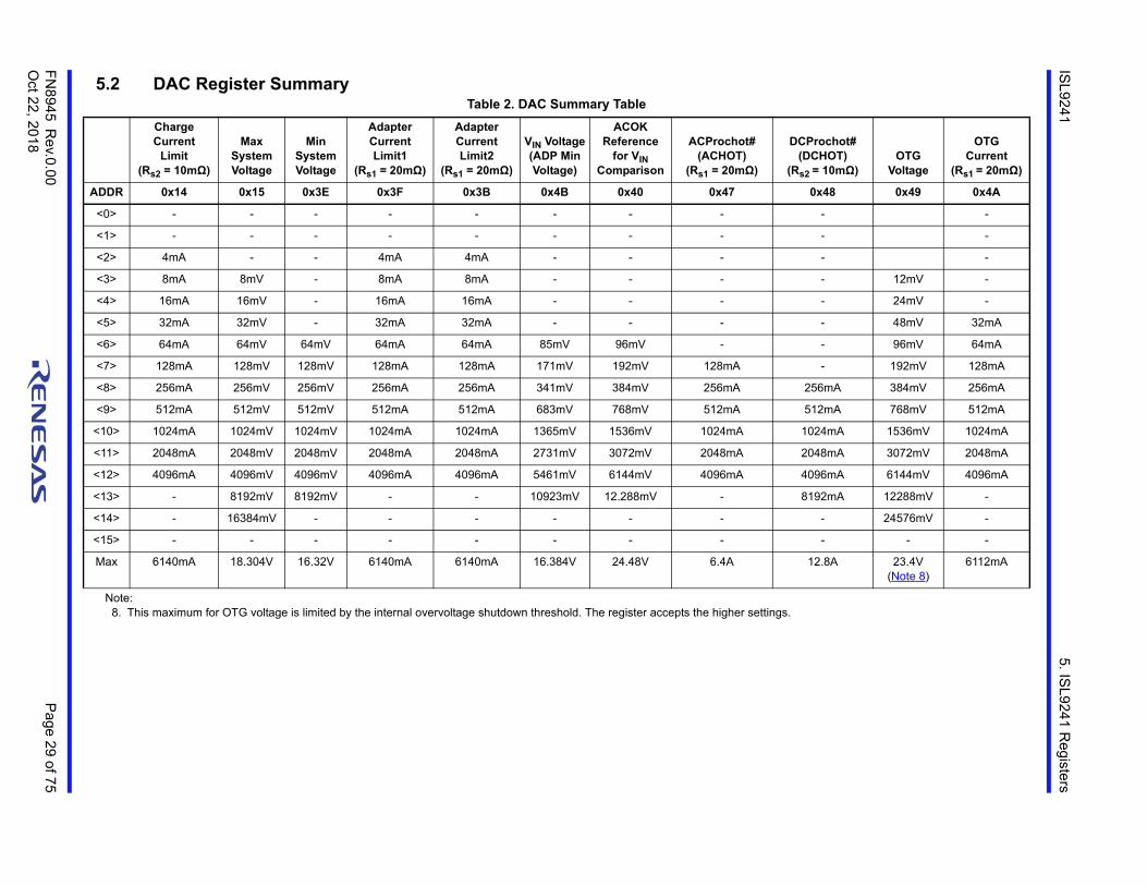
rs5.2 DAC Register Summary
Table 2. DAC Summary Table
Charge Current
Limit(Rs2 = 10mΩ)
Max SystemVoltage
Min SystemVoltage
Adapter CurrentLimit1
(Rs1 = 20mΩ)
Adapter CurrentLimit2
(Rs1 = 20mΩ)
VIN Voltage(ADP Min Voltage)
ACOK Reference
for VIN Comparison
ACProchot#(ACHOT)
(Rs1 = 20mΩ)
DCProchot#(DCHOT)
(Rs2 = 10mΩ)OTG
Voltage
OTGCurrent
(Rs1 = 20mΩ)
ADDR 0x14 0x15 0x3E 0x3F 0x3B 0x4B 0x40 0x47 0x48 0x49 0x4A
<0> - - - - - - - - - -
<1> - - - - - - - - - -
<2> 4mA - - 4mA 4mA - - - - -
<3> 8mA 8mV - 8mA 8mA - - - - 12mV -
<4> 16mA 16mV - 16mA 16mA - - - - 24mV -
<5> 32mA 32mV - 32mA 32mA - - - - 48mV 32mA
<6> 64mA 64mV 64mV 64mA 64mA 85mV 96mV - - 96mV 64mA
<7> 128mA 128mV 128mV 128mA 128mA 171mV 192mV 128mA - 192mV 128mA
<8> 256mA 256mV 256mV 256mA 256mA 341mV 384mV 256mA 256mA 384mV 256mA
<9> 512mA 512mV 512mV 512mA 512mA 683mV 768mV 512mA 512mA 768mV 512mA
<10> 1024mA 1024mV 1024mV 1024mA 1024mA 1365mV 1536mV 1024mA 1024mA 1536mV 1024mA
<11> 2048mA 2048mV 2048mV 2048mA 2048mA 2731mV 3072mV 2048mA 2048mA 3072mV 2048mA
<12> 4096mA 4096mV 4096mV 4096mA 4096mA 5461mV 6144mV 4096mA 4096mA 6144mV 4096mA
<13> - 8192mV 8192mV - - 10923mV 12.288mV - 8192mA 12288mV -
<14> - 16384mV - - - - - - - 24576mV -
<15> - - - - - - - - - - -
Max 6140mA 18.304V 16.32V 6140mA 6140mA 16.384V 24.48V 6.4A 12.8A 23.4V(Note 8)
6112mA
Note:8. This maximum for OTG voltage is limited by the internal overvoltage shutdown threshold. The register accepts the higher settings.
FN8945 Rev.0.00 Page 30 of 75Oct 22, 2018
ISL9241 5. ISL9241 Registers
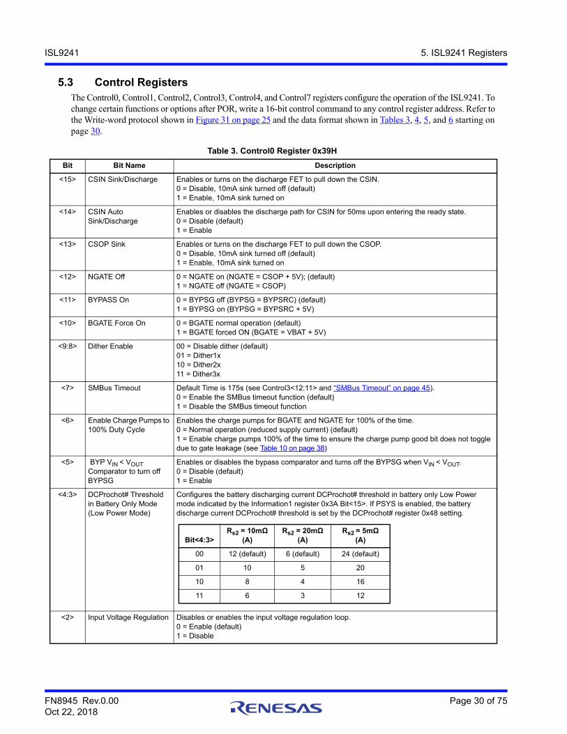
5.3 Control RegistersThe Control0, Control1, Control2, Control3, Control4, and Control7 registers configure the operation of the ISL9241. To change certain functions or options after POR, write a 16-bit control command to any control register address. Refer to the Write-word protocol shown in Figure 31 on page 25 and the data format shown in Tables 3, 4, 5, and 6 starting on page 30.
Table 3. Control0 Register 0x39H
Bit Bit Name Description
<15> CSIN Sink/Discharge Enables or turns on the discharge FET to pull down the CSIN.0 = Disable, 10mA sink turned off (default)1 = Enable, 10mA sink turned on
<14> CSIN Auto Sink/Discharge
Enables or disables the discharge path for CSIN for 50ms upon entering the ready state.0 = Disable (default)1 = Enable
<13> CSOP Sink Enables or turns on the discharge FET to pull down the CSOP.0 = Disable, 10mA sink turned off (default)1 = Enable, 10mA sink turned on
<12> NGATE Off 0 = NGATE on (NGATE = CSOP + 5V); (default)1 = NGATE off (NGATE = CSOP)
<11> BYPASS On 0 = BYPSG off (BYPSG = BYPSRC) (default)1 = BYPSG on (BYPSG = BYPSRC + 5V)
<10> BGATE Force On 0 = BGATE normal operation (default)1 = BGATE forced ON (BGATE = VBAT + 5V)
<9:8> Dither Enable 00 = Disable dither (default)01 = Dither1x10 = Dither2x11 = Dither3x
<7> SMBus Timeout Default Time is 175s (see Control3<12:11> and “SMBus Timeout” on page 45).0 = Enable the SMBus timeout function (default)1 = Disable the SMBus timeout function
<6> Enable Charge Pumps to 100% Duty Cycle
Enables the charge pumps for BGATE and NGATE for 100% of the time.0 = Normal operation (reduced supply current) (default)1 = Enable charge pumps 100% of the time to ensure the charge pump good bit does not toggle due to gate leakage (see Table 10 on page 38)
<5> BYP VIN < VOUT Comparator to turn off BYPSG
Enables or disables the bypass comparator and turns off the BYPSG when VIN < VOUT.0 = Disable (default)1 = Enable
<4:3> DCProchot# Threshold in Battery Only Mode(Low Power Mode)
Configures the battery discharging current DCProchot# threshold in battery only Low Power mode indicated by the Information1 register 0x3A Bit<15>. If PSYS is enabled, the battery discharge current DCProchot# threshold is set by the DCProchot# register 0x48 setting.
<2> Input Voltage Regulation Disables or enables the input voltage regulation loop.0 = Enable (default)1 = Disable
Bit<4:3>Rs2 = 10mΩ
(A)Rs2 = 20mΩ
(A)Rs2 = 5mΩ
(A)
00 12 (default) 6 (default) 24 (default)
01 10 5 20
10 8 4 16
11 6 3 12
FN8945 Rev.0.00 Page 31 of 75Oct 22, 2018
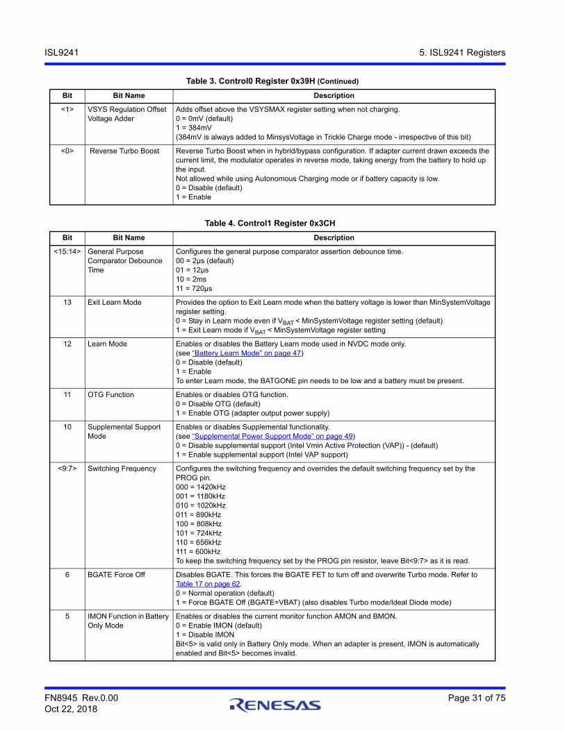
ISL9241 5. ISL9241 Registers
<1> VSYS Regulation Offset Voltage Adder
Adds offset above the VSYSMAX register setting when not charging. 0 = 0mV (default)1 = 384mV (384mV is always added to MinsysVoltage in Trickle Charge mode - irrespective of this bit)
<0> Reverse Turbo Boost Reverse Turbo Boost when in hybrid/bypass configuration. If adapter current drawn exceeds the current limit, the modulator operates in reverse mode, taking energy from the battery to hold up the input.Not allowed while using Autonomous Charging mode or if battery capacity is low.0 = Disable (default)1 = Enable
Table 4. Control1 Register 0x3CH
Bit Bit Name Description
<15:14> General Purpose Comparator Debounce Time
Configures the general purpose comparator assertion debounce time.00 = 2µs (default)01 = 12µs10 = 2ms11 = 720µs
13 Exit Learn Mode Provides the option to Exit Learn mode when the battery voltage is lower than MinSystemVoltage register setting.0 = Stay in Learn mode even if VBAT < MinSystemVoltage register setting (default)1 = Exit Learn mode if VBAT < MinSystemVoltage register setting
12 Learn Mode Enables or disables the Battery Learn mode used in NVDC mode only.(see “Battery Learn Mode” on page 47) 0 = Disable (default)1 = EnableTo enter Learn mode, the BATGONE pin needs to be low and a battery must be present.
11 OTG Function Enables or disables OTG function.0 = Disable OTG (default)1 = Enable OTG (adapter output power supply)
10 Supplemental Support Mode
Enables or disables Supplemental functionality. (see “Supplemental Power Support Mode” on page 49)0 = Disable supplemental support (Intel Vmin Active Protection (VAP)) - (default)1 = Enable supplemental support (Intel VAP support)
<9:7> Switching Frequency Configures the switching frequency and overrides the default switching frequency set by the PROG pin.000 = 1420kHz001 = 1180kHz010 = 1020kHz011 = 890kHz100 = 808kHz101 = 724kHz110 = 656kHz111 = 600kHzTo keep the switching frequency set by the PROG pin resistor, leave Bit<9:7> as it is read.
6 BGATE Force Off Disables BGATE. This forces the BGATE FET to turn off and overwrite Turbo mode. Refer to Table 17 on page 62.0 = Normal operation (default)1 = Force BGATE Off (BGATE=VBAT) (also disables Turbo mode/Ideal Diode mode)
5 IMON Function in Battery Only Mode
Enables or disables the current monitor function AMON and BMON.0 = Enable IMON (default)1 = Disable IMONBit<5> is valid only in Battery Only mode. When an adapter is present, IMON is automatically enabled and Bit<5> becomes invalid.
Table 3. Control0 Register 0x39H (Continued)
Bit Bit Name Description
FN8945 Rev.0.00 Page 32 of 75Oct 22, 2018
ISL9241 5. ISL9241 Registers
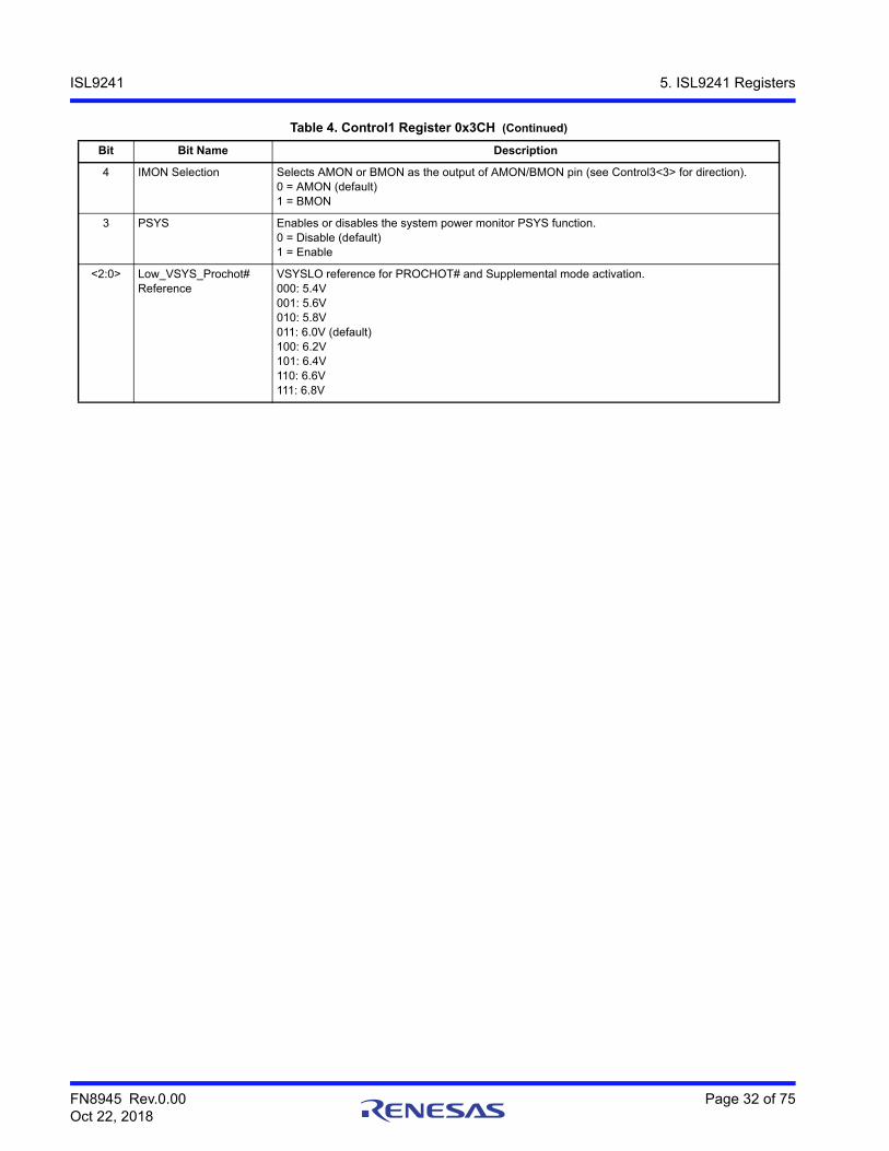
4 IMON Selection Selects AMON or BMON as the output of AMON/BMON pin (see Control3<3> for direction).0 = AMON (default)1 = BMON
3 PSYS Enables or disables the system power monitor PSYS function.0 = Disable (default)1 = Enable
<2:0> Low_VSYS_Prochot# Reference
VSYSLO reference for PROCHOT# and Supplemental mode activation.000: 5.4V001: 5.6V010: 5.8V011: 6.0V (default)100: 6.2V101: 6.4V110: 6.6V111: 6.8V
Table 4. Control1 Register 0x3CH (Continued)
Bit Bit Name Description
FN8945 Rev.0.00 Page 33 of 75Oct 22, 2018
ISL9241 5. ISL9241 Registers
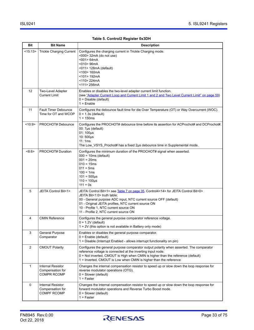
Table 5. Control2 Register 0x3DH
Bit Bit Name Description
<15:13> Trickle Charging Current Configures the charging current in Trickle Charging mode.<000> 32mA (do not use)<001> 64mA<010> 96mA<011> 128mA (default)<100> 160mA<101> 192mA<110> 224mA<111> 256mA
12 Two-Level Adapter Current Limit
Enables or disables the two-level adapter current limit function.(see “Adapter Current Loop and Current Limit 1 and 2 and Two Level Current Limit” on page 59)0 = Disable (default)1 = Enable
11 Fault Timer Debounce Time for OT and WCOP
Configures the debounce fault time for die Over Temperature (OT) or Way Overcurrent (WOC).0 = 1.3s (default)1 = 150ms
<10:9> PROCHOT# Debounce Configures the PROCHOT# debounce time before its assertion for ACProchot# and DCProchot#.00: 7µs (default)01: 100µs 10: 500µs11: 1msThe Low_VSYS_Prochot# has a fixed 2µs debounce time in Supplemental mode.
<8:6> PROCHOT# Duration Configures the minimum duration of the PROCHOT# signal when asserted.000 = 10ms (default)001 = 20ms010 = 15ms011 = 5ms100 = 1ms101 = 500µs110 = 100µs111 = 0s
5 JEITA Control Bit<1> JEITA Control Bit<1> see Table 7 on page 35, Control4<14> for JEITA Control Bit<0>JEITA Bit<1:0> truth table;00 - General purpose ADC input, NTC current source OFF (default)01 - Original JEITA profiles, NTC current source ON10 - Profile 1, NTC current source ON11 - Profile 2, NTC current source ON
4 CMIN Reference Configures the general purpose comparator reference voltage.0 = 1.2V (default)1 = 2V (this option is not available in Battery only mode)
3 General Purpose Comparator
Enables or disables the general purpose comparator.0 = Enable (default)1 = Disable (Interrupt Enabled - allows interrupt functionality on pin)
2 CMOUT Polarity Configures the general purpose comparator output polarity when asserted. The comparator reference voltage is connected at the inverting input node.0 = Not inverted, CMOUT is High when CMIN is higher than the reference (default)1 = Inverted, CMOUT is Low when CMIN is higher than the reference
1 Internal Resistor Compensation for COMPR RCOMP
Changes the internal compensation resistor to speed up or slow down the loop response for reverse modulator operations (OTG).0 = Slower (default)1 = Faster
0 Internal Resistor Compensation for COMPF RCOMP
Changes the internal compensation resistor to speed up or slow down the loop response for forward modulator operations and Reverse Turbo Boost mode.0 = Slower (default)1 = Faster
FN8945 Rev.0.00 Page 34 of 75Oct 22, 2018
ISL9241 5. ISL9241 Registers
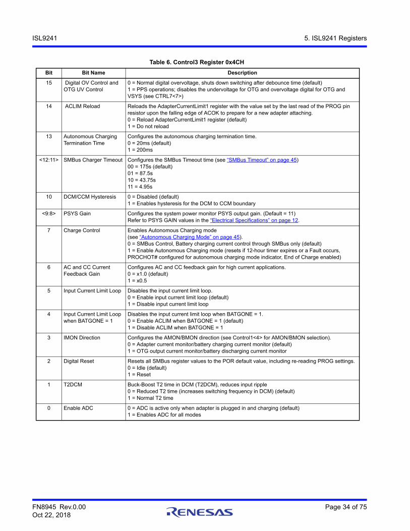
Table 6. Control3 Register 0x4CH
Bit Bit Name Description
15 Digital OV Control and OTG UV Control
0 = Normal digital overvoltage, shuts down switching after debounce time (default)1 = PPS operations; disables the undervoltage for OTG and overvoltage digital for OTG and VSYS (see CTRL7<7>)
14 ACLIM Reload Reloads the AdapterCurrentLimit1 register with the value set by the last read of the PROG pin resistor upon the falling edge of ACOK to prepare for a new adapter attaching. 0 = Reload AdapterCurrentLimit1 register (default)1 = Do not reload
13 Autonomous Charging Termination Time
Configures the autonomous charging termination time.0 = 20ms (default)1 = 200ms
<12:11> SMBus Charger Timeout Configures the SMBus Timeout time (see “SMBus Timeout” on page 45)00 = 175s (default)01 = 87.5s 10 = 43.75s11 = 4.95s
10 DCM/CCM Hysteresis 0 = Disabled (default)1 = Enables hysteresis for the DCM to CCM boundary
<9:8> PSYS Gain Configures the system power monitor PSYS output gain. (Default = 11)Refer to PSYS GAIN values in the “Electrical Specifications” on page 12.
7 Charge Control Enables Autonomous Charging mode(see “Autonomous Charging Mode” on page 45).0 = SMBus Control, Battery charging current control through SMBus only (default)1 = Enable Autonomous Charging mode (resets if 12-hour timer expires or a Fault occurs, PROCHOT# configured for autonomous charging mode indicator, End of Charge enabled)
6 AC and CC Current Feedback Gain
Configures AC and CC feedback gain for high current applications.0 = x1.0 (default)1 = x0.5
5 Input Current Limit Loop Disables the input current limit loop.0 = Enable input current limit loop (default)1 = Disable input current limit loop
4 Input Current Limit Loop when BATGONE = 1
Disables the input current limit loop when BATGONE = 1.0 = Enable ACLIM when BATGONE = 1 (default)1 = Disable ACLIM when BATGONE = 1
3 IMON Direction Configures the AMON/BMON direction (see Control1<4> for AMON/BMON selection).0 = Adapter current monitor/battery charging current monitor (default)1 = OTG output current monitor/battery discharging current monitor
2 Digital Reset Resets all SMBus register values to the POR default value, including re-reading PROG settings.0 = Idle (default)1 = Reset
1 T2DCM Buck-Boost T2 time in DCM (T2DCM), reduces input ripple 0 = Reduced T2 time (increases switching frequency in DCM) (default)1 = Normal T2 time
0 Enable ADC 0 = ADC is active only when adapter is plugged in and charging (default)1 = Enables ADC for all modes
FN8945 Rev.0.00 Page 35 of 75Oct 22, 2018
ISL9241 5. ISL9241 Registers
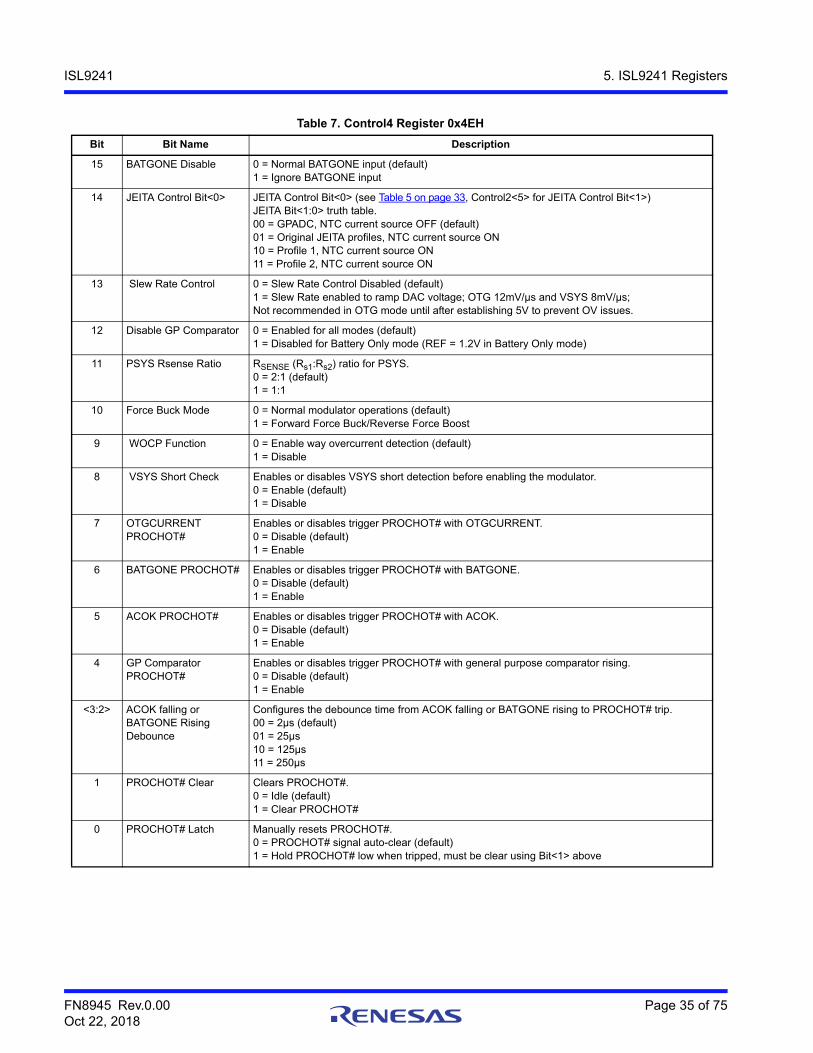
Table 7. Control4 Register 0x4EH
Bit Bit Name Description
15 BATGONE Disable 0 = Normal BATGONE input (default)1 = Ignore BATGONE input
14 JEITA Control Bit<0> JEITA Control Bit<0> (see Table 5 on page 33, Control2<5> for JEITA Control Bit<1>)JEITA Bit<1:0> truth table.00 = GPADC, NTC current source OFF (default)01 = Original JEITA profiles, NTC current source ON10 = Profile 1, NTC current source ON11 = Profile 2, NTC current source ON
13 Slew Rate Control 0 = Slew Rate Control Disabled (default)1 = Slew Rate enabled to ramp DAC voltage; OTG 12mV/µs and VSYS 8mV/µs; Not recommended in OTG mode until after establishing 5V to prevent OV issues.
12 Disable GP Comparator 0 = Enabled for all modes (default)1 = Disabled for Battery Only mode (REF = 1.2V in Battery Only mode)
11 PSYS Rsense Ratio RSENSE (Rs1:Rs2) ratio for PSYS.0 = 2:1 (default)1 = 1:1
10 Force Buck Mode 0 = Normal modulator operations (default)1 = Forward Force Buck/Reverse Force Boost
9 WOCP Function 0 = Enable way overcurrent detection (default)1 = Disable
8 VSYS Short Check Enables or disables VSYS short detection before enabling the modulator.0 = Enable (default)1 = Disable
7 OTGCURRENT PROCHOT#
Enables or disables trigger PROCHOT# with OTGCURRENT.0 = Disable (default)1 = Enable
6 BATGONE PROCHOT# Enables or disables trigger PROCHOT# with BATGONE.0 = Disable (default)1 = Enable
5 ACOK PROCHOT# Enables or disables trigger PROCHOT# with ACOK.0 = Disable (default)1 = Enable
4 GP Comparator PROCHOT#
Enables or disables trigger PROCHOT# with general purpose comparator rising.0 = Disable (default)1 = Enable
<3:2> ACOK falling or BATGONE Rising Debounce
Configures the debounce time from ACOK falling or BATGONE rising to PROCHOT# trip.00 = 2µs (default)01 = 25µs10 = 125µs11 = 250µs
1 PROCHOT# Clear Clears PROCHOT#.0 = Idle (default)1 = Clear PROCHOT#
0 PROCHOT# Latch Manually resets PROCHOT#.0 = PROCHOT# signal auto-clear (default)1 = Hold PROCHOT# low when tripped, must be clear using Bit<1> above
FN8945 Rev.0.00 Page 36 of 75Oct 22, 2018
ISL9241 5. ISL9241 Registers
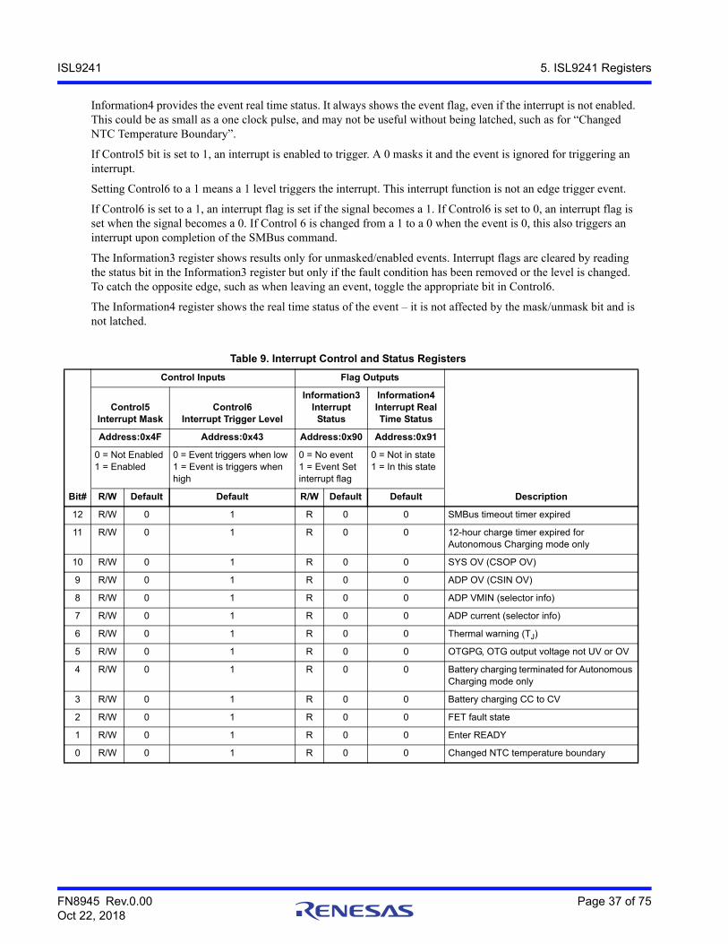
5.4 Interrupt FunctionalityThe INT# pin is shared with the CMOUT pins, so it must be enabled by setting Control2 Bit<3> = 1 (see Table 5). Setting the bit to 1 disables the comparator output function. After the INT# pin is enabled configure the faults or flags to be masked or unmasked and have the INT# trigger. If the flag is a fault, it must be read to clear the INT#. Thirteen possible functions are supported by the interrupt control registers. INT# is an active low, open-drain output that is shared with the GP comparator. It pulls low to signal an interrupt event and requires a pull-up source to toggle.
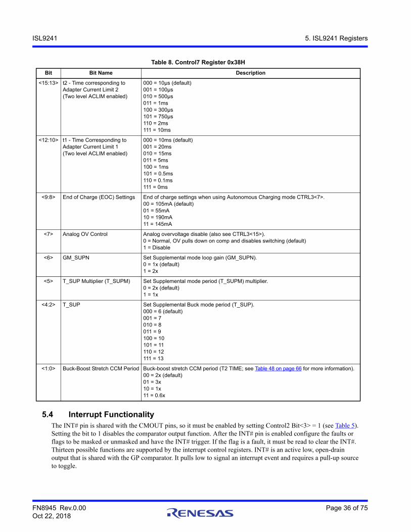
Table 8. Control7 Register 0x38H
Bit Bit Name Description
<15:13> t2 - Time corresponding to Adapter Current Limit 2(Two level ACLIM enabled)
000 = 10µs (default)001 = 100µs010 = 500µs011 = 1ms100 = 300µs101 = 750µs110 = 2ms111 = 10ms
<12:10> t1 - Time Corresponding to Adapter Current Limit 1(Two level ACLIM enabled)
000 = 10ms (default)001 = 20ms010 = 15ms011 = 5ms100 = 1ms101 = 0.5ms110 = 0.1ms111 = 0ms
<9:8> End of Charge (EOC) Settings End of charge settings when using Autonomous Charging mode CTRL3<7>.00 = 105mA (default)01 = 55mA10 = 190mA11 = 145mA
<7> Analog OV Control Analog overvoltage disable (also see CTRL3<15>).0 = Normal, OV pulls down on comp and disables switching (default)1 = Disable
<6> GM_SUPN Set Supplemental mode loop gain (GM_SUPN).0 = 1x (default)1 = 2x
<5> T_SUP Multiplier (T_SUPM) Set Supplemental mode period (T_SUPM) multiplier.0 = 2x (default)1 = 1x
<4:2> T_SUP Set Supplemental Buck mode period (T_SUP).000 = 6 (default)001 = 7010 = 8011 = 9100 = 10101 = 11110 = 12111 = 13
<1:0> Buck-Boost Stretch CCM Period Buck-boost stretch CCM period (T2 TIME; see Table 48 on page 66 for more information).00 = 2x (default)01 = 3x10 = 1x11 = 0.6x
FN8945 Rev.0.00 Page 37 of 75Oct 22, 2018
ISL9241 5. ISL9241 Registers
Information4 provides the event real time status. It always shows the event flag, even if the interrupt is not enabled. This could be as small as a one clock pulse, and may not be useful without being latched, such as for “Changed NTC Temperature Boundary”.
If Control5 bit is set to 1, an interrupt is enabled to trigger. A 0 masks it and the event is ignored for triggering an interrupt.
Setting Control6 to a 1 means a 1 level triggers the interrupt. This interrupt function is not an edge trigger event.
If Control6 is set to a 1, an interrupt flag is set if the signal becomes a 1. If Control6 is set to 0, an interrupt flag is set when the signal becomes a 0. If Control 6 is changed from a 1 to a 0 when the event is 0, this also triggers an interrupt upon completion of the SMBus command.
The Information3 register shows results only for unmasked/enabled events. Interrupt flags are cleared by reading the status bit in the Information3 register but only if the fault condition has been removed or the level is changed. To catch the opposite edge, such as when leaving an event, toggle the appropriate bit in Control6.
The Information4 register shows the real time status of the event – it is not affected by the mask/unmask bit and is not latched.
Table 9. Interrupt Control and Status Registers
Bit#
Control Inputs Flag Outputs
Description
Control5Interrupt Mask
Control6Interrupt Trigger Level
Information3Interrupt
Status
Information4 Interrupt Real Time Status
Address:0x4F Address:0x43 Address:0x90 Address:0x91
0 = Not Enabled1 = Enabled
0 = Event triggers when low1 = Event is triggers when high
0 = No event1 = Event Set interrupt flag
0 = Not in state 1 = In this state
R/W Default Default R/W Default Default
12 R/W 0 1 R 0 0 SMBus timeout timer expired
11 R/W 0 1 R 0 0 12-hour charge timer expired for Autonomous Charging mode only
10 R/W 0 1 R 0 0 SYS OV (CSOP OV)
9 R/W 0 1 R 0 0 ADP OV (CSIN OV)
8 R/W 0 1 R 0 0 ADP VMIN (selector info)
7 R/W 0 1 R 0 0 ADP current (selector info)
6 R/W 0 1 R 0 0 Thermal warning (TJ)
5 R/W 0 1 R 0 0 OTGPG, OTG output voltage not UV or OV
4 R/W 0 1 R 0 0 Battery charging terminated for Autonomous Charging mode only
3 R/W 0 1 R 0 0 Battery charging CC to CV
2 R/W 0 1 R 0 0 FET fault state
1 R/W 0 1 R 0 0 Enter READY
0 R/W 0 1 R 0 0 Changed NTC temperature boundary
FN8945 Rev.0.00 Page 38 of 75Oct 22, 2018
ISL9241 5. ISL9241 Registers
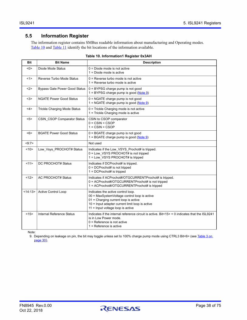
5.5 Information RegisterThe information register contains SMBus readable information about manufacturing and Operating modes. Table 10 and Table 11 identify the bit locations of the information available.
Table 10. Information1 Register 0x3AH
Bit Bit Name Description
<0> Diode Mode Status 0 = Diode mode is not active1 = Diode mode is active
<1> Reverse Turbo Mode Status 0 = Reverse turbo mode is not active1 = Reverse turbo mode is active
<2> Bypass Gate Power Good Status 0 = BYPSG charge pump is not good1 = BYPSG charge pump is good (Note 9)
<3> NGATE Power Good Status 0 = NGATE charge pump is not good1 = NGATE charge pump is good (Note 9)
<4> Trickle Charging Mode Status 0 = Trickle Charging mode is not active1 = Trickle Charging mode is active
<5> CSIN_CSOP Comparator Status CSIN to CSOP comparator0 = CSIN < CSOP1 = CSIN > CSOP
<6> BGATE Power Good Status 0 = BGATE charge pump is not good1 = BGATE charge pump is good (Note 9)
<9:7> Not used
<10> Low_Vsys_PROCHOT# Status Indicates if the Low_VSYS_Prochot# is tripped.0 = Low_VSYS PROCHOT# is not tripped1 = Low_VSYS PROCHOT# is tripped
<11> DC PROCHOT# Status Indicates if DCProchot# is tripped.0 = DCProchot# is not tripped1 = DCProchot# is tripped
<12> AC PROCHOT# Status Indicates if ACProchot#/OTGCURRENTProchot# is tripped.0 = ACProchot#/OTGCURRENTProchot# is not tripped1 = ACProchot#/OTGCURRENTProchot# is tripped
<14:13> Active Control Loop Indicates the active control loop.00 = MaxSystemVoltage control loop is active01 = Charging current loop is active10 = Input adapter current limit loop is active11 = Input voltage loop is active
<15> Internal Reference Status Indicates if the internal reference circuit is active. Bit<15> = 0 indicates that the ISL9241 is in Low Power mode.0 = Reference is not active1 = Reference is active
Note:9. Depending on leakage on pin, the bit may toggle unless set to 100% charge pump mode using CTRL3 Bit<6> (see Table 3 on
page 30).
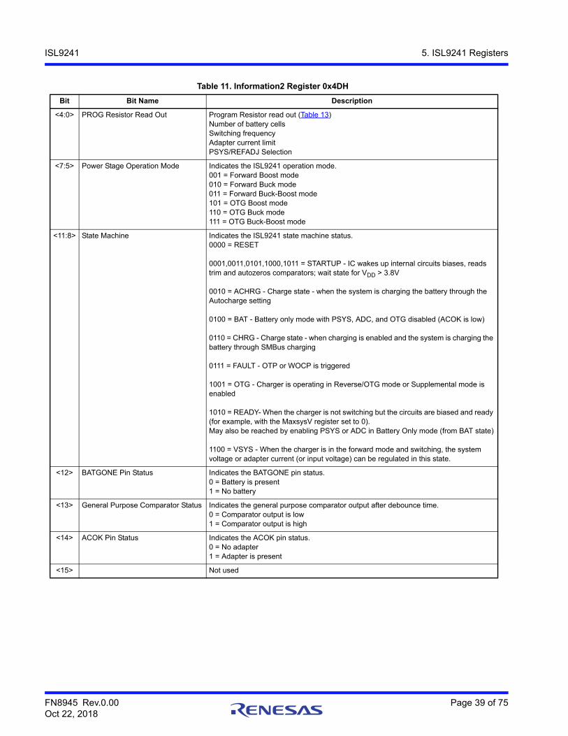
FN8945 Rev.0.00 Page 39 of 75Oct 22, 2018
ISL9241 5. ISL9241 Registers
Table 11. Information2 Register 0x4DH
Bit Bit Name Description
<4:0> PROG Resistor Read Out Program Resistor read out (Table 13)Number of battery cellsSwitching frequencyAdapter current limitPSYS/REFADJ Selection
<7:5> Power Stage Operation Mode Indicates the ISL9241 operation mode.001 = Forward Boost mode010 = Forward Buck mode011 = Forward Buck-Boost mode101 = OTG Boost mode110 = OTG Buck mode111 = OTG Buck-Boost mode
<11:8> State Machine Indicates the ISL9241 state machine status.0000 = RESET
0001,0011,0101,1000,1011 = STARTUP - IC wakes up internal circuits biases, reads trim and autozeros comparators; wait state for VDD > 3.8V
0010 = ACHRG - Charge state - when the system is charging the battery through the Autocharge setting
0100 = BAT - Battery only mode with PSYS, ADC, and OTG disabled (ACOK is low)
0110 = CHRG - Charge state - when charging is enabled and the system is charging the battery through SMBus charging
0111 = FAULT - OTP or WOCP is triggered
1001 = OTG - Charger is operating in Reverse/OTG mode or Supplemental mode is enabled
1010 = READY- When the charger is not switching but the circuits are biased and ready (for example, with the MaxsysV register set to 0). May also be reached by enabling PSYS or ADC in Battery Only mode (from BAT state)
1100 = VSYS - When the charger is in the forward mode and switching, the system voltage or adapter current (or input voltage) can be regulated in this state.
<12> BATGONE Pin Status Indicates the BATGONE pin status.0 = Battery is present1 = No battery
<13> General Purpose Comparator Status Indicates the general purpose comparator output after debounce time.0 = Comparator output is low1 = Comparator output is high
<14> ACOK Pin Status Indicates the ACOK pin status.0 = No adapter1 = Adapter is present
<15> Not used
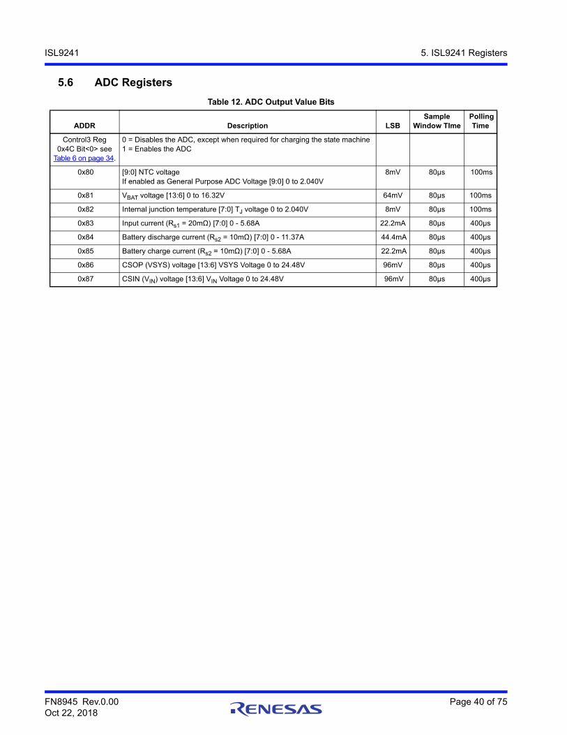
FN8945 Rev.0.00 Page 40 of 75Oct 22, 2018
ISL9241 5. ISL9241 Registers
5.6 ADC Registers
Table 12. ADC Output Value Bits
ADDR Description LSBSample
Window TIme Polling
Time
Control3 Reg 0x4C Bit<0> see
Table 6 on page 34.
0 = Disables the ADC, except when required for charging the state machine1 = Enables the ADC
0x80 [9:0] NTC voltageIf enabled as General Purpose ADC Voltage [9:0] 0 to 2.040V
8mV 80µs 100ms
0x81 VBAT voltage [13:6] 0 to 16.32V 64mV 80µs 100ms
0x82 Internal junction temperature [7:0] TJ voltage 0 to 2.040V 8mV 80µs 100ms
0x83 Input current (Rs1 = 20mΩ)[7:0] 0 - 5.68A 22.2mA 80µs 400µs
0x84 Battery discharge current (Rs2 = 10mΩ) [7:0] 0 - 11.37A 44.4mA 80µs 400µs
0x85 Battery charge current (Rs2 = 10mΩ) [7:0] 0 - 5.68A 22.2mA 80µs 400µs
0x86 CSOP (VSYS) voltage [13:6] VSYS Voltage 0 to 24.48V 96mV 80µs 400µs
0x87 CSIN (VIN) voltage [13:6] VIN Voltage 0 to 24.48V 96mV 80µs 400µs
FN8945 Rev.0.00 Page 41 of 75Oct 22, 2018
ISL9241 6. Application Information
6. Application Information
6.1 Start-Up and ACOKThe ISL9241 includes a low power LDO with a nominal 4.7V output and an internal input OR-ed from the VBAT and CSIN inputs. The ISL9241 also includes a high power LDO with a nominal 5V output that has an input from the DCIN pin connected both to the adapter and the system bus through an external OR-ing diode circuit. The low power LDO must be active above 2.7V to enable the high power LDO. Both LDO outputs are tied to the VDD pin to provide the bias power and gate drive power for the ISL9241. The VDDP pin is the ISL9241 gate drive power supply input. Use an RC filter to generate the VDDP pin voltage from the VDD pin voltage.
The ISL9241 monitors the CSIN pin voltage to determine the presence of the adapter. When CSIN is higher than the ACOK threshold and after VDD POR releases, the charger is initialized for 150ms of debounce time. Initialization takes about 4ms , and next the trim settings are read, the internal circuitry is autozeroed, and configuration is completed during the STARTUP state (see Table 11 on page 39). During the first time an adapter is plugged in, while the 150ms debounce time is running, the ISL9241 uses a Renesas technique to check if the VSYS output is shorted (see “System Voltage Rail Short Protection” on page 54).
When VDD > 2.7V, the ISL9241 digital block is activated and the SMBus register is ready to communicate with the master controller.
When the ISL9241 turns on the LDOs, it sources a current out of the PROG pin and reads the pin voltage to determine the PROG resistor value. The PROG resistor programs the configurations of the ISL9241. Refer to Table 13 on page 42.
When VDD > 3.8V, the ISL9241 allows the external circuit to pull up the ACOK pin. When ACOK is asserted, ISL9241 starts switching.
The ACOK is an open-drain output pin indicating the presence of the adapter and readiness of the adapter to supply power to the system bus. The ISL9241 actively pulls ACOK low in the absence of the adapter or for Way Overcurrent (WCOP) or for Over-Temperature (OTP).
Two thresholds affect ACOK. The higher of the two is in control of ACOK. One threshold is fixed at 3.6V rising and one programmable threshold using the DAC (refer to Table 2 on page 29 for the ACOK Ref register). Register 0x40 value sets the threshold. The default register value is set to 0x0000h, which disables the programmable threshold detection. The programmable threshold is helpful for monitoring the input supply when targeting higher voltages with USB Power Delivery communications. To detect an unplugged adapter, the adapter voltage has to fall below the ACOK threshold (higher of 3.4V falling and ACOK Ref register value).
CSIN voltage should be higher than ACOK threshold, and VDD should be higher than 3.8V for switching to start and continue.
In Battery Only mode, the ISL9241 enters Low Power mode if only the battery is present. VDD is 4.5V from the low power LDO to minimize the power consumption. VDD becomes 5V when it exits Low Power mode, such as when PSYS or ADC are enabled.
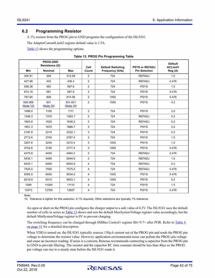
FN8945 Rev.0.00 Page 42 of 75Oct 22, 2018
ISL9241 6. Application Information
6.2 Programming ResistorA 1% resistor from the PROG pin to GND programs the configuration of the ISL9241.
The AdapterCurrentLimit2 register default value is 1.5A.
Table 13 shows the programming options.
An open or short on the PROG pin configures the charger output to a safe value of 4.2V. The ISL9241 uses the default number of cells in series as Table 13 shows and sets the default MaxSystemVoltage register value accordingly, but the default MinSystemVoltage register is 0V to prevent charging.
The switching frequency can be changed through SMBus Control1 register Bit<9:7> after POR. Refer to Table 4 on page 31 for a detailed description.
When VDD is turned on, the ISL9241 typically sources 130µA current out of the PROG pin and reads the PROG pin voltage to determine the resistor value. However, application environmental noise can pollute the PROG pin voltage and cause an incorrect reading. If noise is a concern, Renesas recommends connecting a capacitor from the PROG pin to GND to provide filtering. The resistor and the capacitor RC time constant should be less than 40µs so the PROG pin voltage can rise to a steady state before the ISL9241 reads it.
Table 13. PROG Pin Programming Table
PROG-GNDResistance (Ω)
Cell Count
Default Switching Frequency (kHz)
PSYS or REFADJ Pin Selection
Default ACLimit1 Reg (A)Min Nominal Max
305.91 309 312.09 2 724 REFADJ 1.5
427.68 432 436.3 2 724 REFADJ 0.476
556.38 562 567.6 2 724 PSYS 1.5
674.19 681 687.8 2 724 PSYS 0.476
797.94 806 814.06 2 1050 PSYS 0.476
930.069(Note 10)
931(Note 10)
931.931(Note 10)
2 1050 PSYS 0.2
1089.0 1100 1111 2 724 PSYS 3.0
1356.3 1370 1383.7 2 724 REFADJ 0.2
1603.8 1620 1636.2 3 724 REFADJ 0.2
1851.3 1870 1888.7 3 724 PSYS 3.0
2187.9 2210 2232.1 3 724 PSYS 0.2
2712.6 2740 2767.4 3 724 PSYS 1.5
3207.6 3240 3272.4 3 1050 PSYS 1.5
3702.6 3740 3777.4 3 1050 PSYS 0.476
4375.8 4420 4464.2 3 724 REFADJ 0.476
5435.1 5490 5544.9 3 724 REFADJ 1.5
6425.1 6490 6554.9 4 724 REFADJ 0.2
7425.0 7500 7575.0 4 724 REFADJ 0.476
8365.5 8450 8534.5 4 1050 PSYS 0.476
9216.9 9310 9403.1 4 1050 PSYS 0.2
1089 11000 11110 4 724 PSYS 1.5
12573 12700 12827 4 724 PSYS 0.476
Note:10. Tolerance is tighter for this selection, 0.1% required. Other selections are typically 1% tolerance.
FN8945 Rev.0.00 Page 43 of 75Oct 22, 2018
ISL9241 6. Application Information
By default, whenever the adapter is unplugged and ACOK goes from high to low, the ISL9241 resets the AdapterCurrentLimit1 register to the default setting determined by the PROG pin resistor. This current limit reloading can be disabled using Control3 Bit <14> as shown in Table 6 on page 34.
If PSYS is not enabled in Battery Only mode, the ISL9241 resets the MaxSystemVoltage register to the default value according to the PROG pin cell number setting. If PSYS is enabled, the ISL9241 keeps the value in the register.
The diagrams in this datasheet are based on current-sensing resistors Rs1 = 20mΩ and Rs2 = 10mΩ unless specified otherwise.
6.3 Charger Control Register Operations
6.3.1 System Voltage Regulation and Maximum Charging Voltage RegulationIf the battery is absent, or if a battery is present but BGATE is turned off, the ISL9241 regulates the system bus voltage at the MaxSystemVoltage register setting or optionally to the MaxSystemVoltage setting plus 384mV. The CSOP pin senses the system bus voltage. When a valid adapter voltage is not present and only the battery is present, the ISL9241 enters a low power state. In this state, the BGATE is turned on, and the charge current is not controlled if VSYS is raised above the battery voltage by an external source connected directly to VSYS. To set the maximum charging voltage or the system regulating voltage, write a 16-bit MaxSystemVoltage command to register address 0x15H using the Write-word protocol shown in Figure 31 on page 25 and the data format shown in Table 2.
The MaxSystemVoltage register accepts any voltage command, but only the valid register bits are written to the register and the maximum value is clamped. A 0x0000H command in REG 0x15H causes the ISL9241 to stop switching and enter READY state.
When the device is not charging but is in the VSYS state and Control0 register Bit<1> is a 0, the system voltage is regulated to the same setting as the DAC. When Control0 register Bit<1> is a 1 then system voltage is regulated to the DAC plus an offset of 384mV, which is useful to avoid discharging a full battery in VSYS state when there is a system load transient.
The MaxSystemVoltage register sets the battery full charging voltage limit. The MaxSystemVoltage register setting is also the system bus voltage regulation point when the battery is absent or present but not in Charging mode. The MinSystemVoltage register setting is also the system voltage regulation point when it is in Trickle Charging mode. The CSOP pin is the system voltage regulation sense point in Trickle Charging mode. Refer to Table 2 on page 29 for more information about the Min System Voltage register.
The CSOP pin senses the battery voltage for maximum charging voltage regulation. The CSOP pin is also the system bus voltage regulation sense point and controls the VSYS operating voltage.
6.3.2 Normal/Fast Battery Charging and Charging Current LimitTo set the charging current limit, write a 16-bit ChargeCurrentLimit command to register address 0x14H (Table 2) using the Write-word protocol shown in Figure 31 on page 25. Set ChargeCurrentLimit = 0 and MinSystemVoltage = 0 to stop charging. Set ChargeCurrent Limit and MinSystemVoltage to non zero to start trickle or fast/normal charging. It is not recommended to set only one of these registers to 0.
By default, the adapter current-sensing resistor, Rs1, is 20mΩ and the battery current-sensing resistor, Rs2, is 10mΩ. Using the Rs1 = 20mΩand Rs2 = 10mΩ option results in a 4mA/LSB correlation in the SMBus current commands.
If the Rs1 and Rs2 values are different from the Rs1 = 20mΩand Rs2 = 10mΩ option, scale the SMBus commands accordingly to obtain the correct current. Smaller current sense resistor values reduce the power loss while larger current sense resistor values give better accuracy. For example, if using a 5mΩ Rs2, multiply each value in the DAC table by 2.
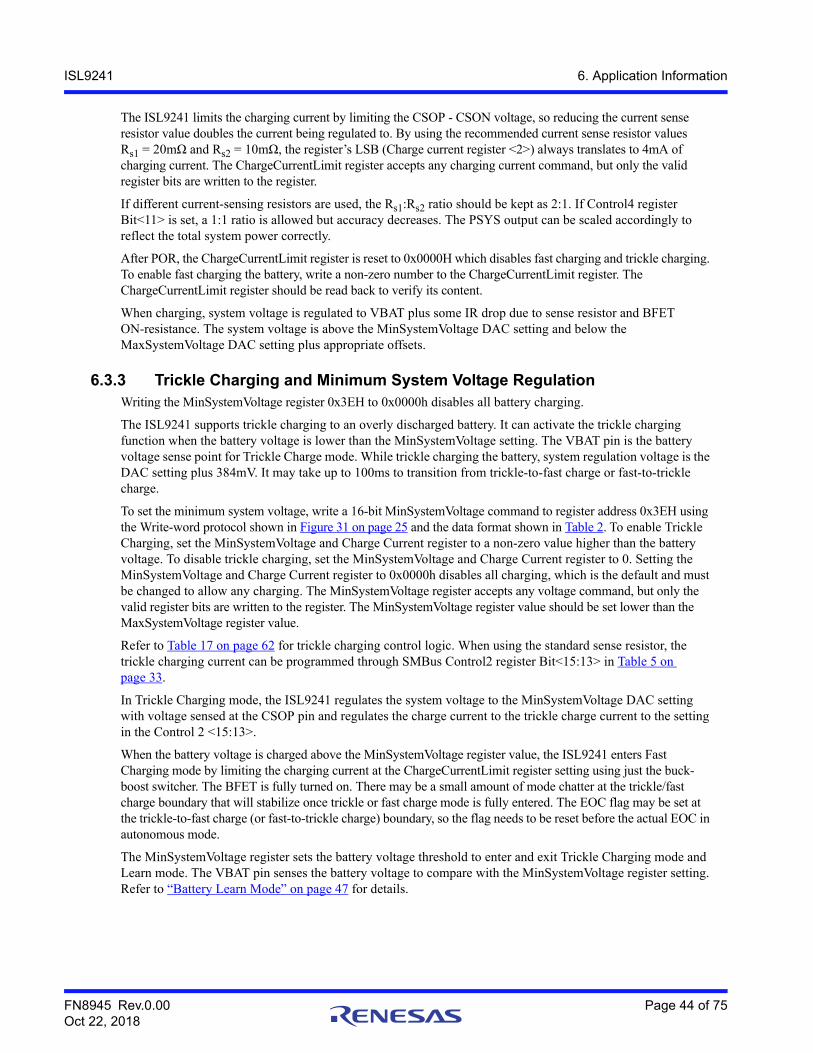
FN8945 Rev.0.00 Page 44 of 75Oct 22, 2018
ISL9241 6. Application Information
The ISL9241 limits the charging current by limiting the CSOP - CSON voltage, so reducing the current sense resistor value doubles the current being regulated to. By using the recommended current sense resistor values Rs1 = 20mΩand Rs2 = 10mΩ, the register’s LSB (Charge current register <2>) always translates to 4mA of charging current. The ChargeCurrentLimit register accepts any charging current command, but only the valid register bits are written to the register.
If different current-sensing resistors are used, the Rs1:Rs2 ratio should be kept as 2:1. If Control4 register Bit<11> is set, a 1:1 ratio is allowed but accuracy decreases. The PSYS output can be scaled accordingly to reflect the total system power correctly.
After POR, the ChargeCurrentLimit register is reset to 0x0000H which disables fast charging and trickle charging. To enable fast charging the battery, write a non-zero number to the ChargeCurrentLimit register. The ChargeCurrentLimit register should be read back to verify its content.
When charging, system voltage is regulated to VBAT plus some IR drop due to sense resistor and BFET ON-resistance. The system voltage is above the MinSystemVoltage DAC setting and below the MaxSystemVoltage DAC setting plus appropriate offsets.
6.3.3 Trickle Charging and Minimum System Voltage RegulationWriting the MinSystemVoltage register 0x3EH to 0x0000h disables all battery charging.
The ISL9241 supports trickle charging to an overly discharged battery. It can activate the trickle charging function when the battery voltage is lower than the MinSystemVoltage setting. The VBAT pin is the battery voltage sense point for Trickle Charge mode. While trickle charging the battery, system regulation voltage is the DAC setting plus 384mV. It may take up to 100ms to transition from trickle-to-fast charge or fast-to-trickle charge.
To set the minimum system voltage, write a 16-bit MinSystemVoltage command to register address 0x3EH using the Write-word protocol shown in Figure 31 on page 25 and the data format shown in Table 2. To enable Trickle Charging, set the MinSystemVoltage and Charge Current register to a non-zero value higher than the battery voltage. To disable trickle charging, set the MinSystemVoltage and Charge Current register to 0. Setting the MinSystemVoltage and Charge Current register to 0x0000h disables all charging, which is the default and must be changed to allow any charging. The MinSystemVoltage register accepts any voltage command, but only the valid register bits are written to the register. The MinSystemVoltage register value should be set lower than the MaxSystemVoltage register value.
Refer to Table 17 on page 62 for trickle charging control logic. When using the standard sense resistor, the trickle charging current can be programmed through SMBus Control2 register Bit<15:13> in Table 5 on page 33.
In Trickle Charging mode, the ISL9241 regulates the system voltage to the MinSystemVoltage DAC setting with voltage sensed at the CSOP pin and regulates the charge current to the trickle charge current to the setting in the Control 2 <15:13>.
When the battery voltage is charged above the MinSystemVoltage register value, the ISL9241 enters Fast Charging mode by limiting the charging current at the ChargeCurrentLimit register setting using just the buck-boost switcher. The BFET is fully turned on. There may be a small amount of mode chatter at the trickle/fast charge boundary that will stabilize once trickle or fast charge mode is fully entered. The EOC flag may be set at the trickle-to-fast charge (or fast-to-trickle charge) boundary, so the flag needs to be reset before the actual EOC in autonomous mode.
The MinSystemVoltage register sets the battery voltage threshold to enter and exit Trickle Charging mode and Learn mode. The VBAT pin senses the battery voltage to compare with the MinSystemVoltage register setting. Refer to “Battery Learn Mode” on page 47 for details.
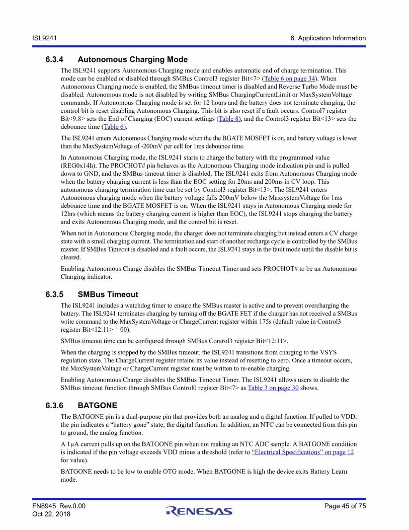
FN8945 Rev.0.00 Page 45 of 75Oct 22, 2018
ISL9241 6. Application Information
6.3.4 Autonomous Charging ModeThe ISL9241 supports Autonomous Charging mode and enables automatic end of charge termination. This mode can be enabled or disabled through SMBus Control3 register Bit<7> (Table 6 on page 34). When Autonomous Charging mode is enabled, the SMBus timeout timer is disabled and Reverse Turbo Mode must be disabled. Autonomous mode is not disabled by writing SMBus ChargingCurrentLimit or MaxSystemVoltage commands. If Autonomous Charging mode is set for 12 hours and the battery does not terminate charging, the control bit is reset disabling Autonomous Charging. This bit is also reset if a fault occurs. Control7 register Bit<9:8> sets the End of Charging (EOC) current settings (Table 8), and the Control3 register Bit<13> sets the debounce time (Table 6).
The ISL9241 enters Autonomous Charging mode when the the BGATE MOSFET is on, and battery voltage is lower than the MaxSystemVoltage of -200mV per cell for 1ms debounce time.
In Autonomous Charging mode, the ISL9241 starts to charge the battery with the programmed value (REG0x14h). The PROCHOT# pin behaves as the Autonomous Charging mode indication pin and is pulled down to GND, and the SMBus timeout timer is disabled. The ISL9241 exits from Autonomous Charging mode when the battery charging current is less than the EOC setting for 20ms and 200ms in CV loop. This autonomous charging termination time can be set by Control3 register Bit<13>. The ISL9241 enters Autonomous charging mode when the battery voltage falls 200mV below the MaxsystemVoltage for 1ms debounce time and the BGATE MOSFET is on. When the ISL9241 stays in Autonomous Charging mode for 12hrs (which means the battery charging current is higher than EOC), the ISL9241 stops charging the battery and exits Autonomous Charging mode, and the control bit is reset.
When not in Autonomous Charging mode, the charger does not terminate charging but instead enters a CV charge state with a small charging current. The termination and start of another recharge cycle is controlled by the SMBus master. If SMBus Timeout is disabled and a fault occurs, the ISL9241 stays in the fault mode until the disable bit is cleared.
Enabling Autonomous Charge disables the SMBus Timeout Timer and sets PROCHOT# to be an Autonomous Charging indicator.
6.3.5 SMBus TimeoutThe ISL9241 includes a watchdog timer to ensure the SMBus master is active and to prevent overcharging the battery. The ISL9241 terminates charging by turning off the BGATE FET if the charger has not received a SMBus write command to the MaxSystemVoltage or ChargeCurrent register within 175s (default value in Control3 register Bit<12:11> = 00).
SMBus timeout time can be configured through SMBus Control3 register Bit<12:11>.
When the charging is stopped by the SMBus timeout, the ISL9241 transitions from charging to the VSYS regulation state. The ChargeCurrent register retains its value instead of resetting to zero. Once a timeout occurs, the MaxSystemVoltage or ChargeCurrent register must be written to re-enable charging.
Enabling Autonomous Charge disables the SMBus Timeout Timer. The ISL9241 allows users to disable the SMBus timeout function through SMBus Control0 register Bit<7> as Table 3 on page 30 shows.
6.3.6 BATGONEThe BATGONE pin is a dual-purpose pin that provides both an analog and a digital function. If pulled to VDD, the pin indicates a “battery gone” state, the digital function. In addition, an NTC can be connected from this pin to ground, the analog function.
A 1µA current pulls up on the BATGONE pin when not making an NTC ADC sample. A BATGONE condition is indicated if the pin voltage exceeds VDD minus a threshold (refer to “Electrical Specifications” on page 12 for value).
BATGONE needs to be low to enable OTG mode. When BATGONE is high the device exits Battery Learn mode.
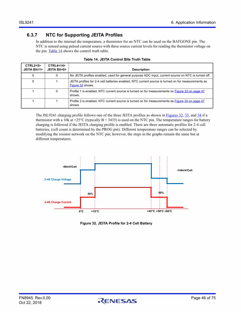
FN8945 Rev.0.00 Page 46 of 75Oct 22, 2018
ISL9241 6. Application Information
6.3.7 NTC for Supporting JEITA Profiles In addition to the internal die temperature, a thermistor for an NTC can be used on the BATGONE pin. The NTC is sensed using pulsed current source with three source current levels for reading the thermistor voltage on the pin. Table 14 shows the control truth table.
The ISL9241 charging profile follows one of the three JEITA profiles as shown in Figures 32, 33, and 34 if a thermistor with a 10k at +25°C (typically B = 3435) is used on the NTC pin. The temperature ranges for battery charging is followed if the JEITA charging profile is enabled. There are three automatic profiles for 2-4 cell batteries, (cell count is determined by the PROG pin). Different temperature ranges can be selected by modifying the resistor network on the NTC pin; however, the steps in the graphs remain the same but at different temperatures.
Table 14. JEITA Control Bits Truth Table
CTRL2<5>JEITA Bit<1>
CTRL4<14>JEITA Bit<0> Description
0 0 No JEITA profiles enabled, used for general purpose ADC input, current source on NTC is turned off.
0 1 JEITA profiles for 2-4 cell batteries enabled, NTC current source is turned on for measurements as Figure 32 shows.
1 0 Profile 1 is enabled, NTC current source is turned on for measurements as Figure 33 on page 47 shows.
1 1 Profile 2 is enabled, NTC current source is turned on for measurements as Figure 34 on page 47 shows.
Figure 32. JEITA Profile for 2-4 Cell Battery
FN8945 Rev.0.00 Page 47 of 75Oct 22, 2018
ISL9241 6. Application Information
6.3.8 Battery Learn ModeThe ISL9241 supports Battery Learn mode when in NVDC mode only. The ISL9241 enters Battery Learn mode when it receives the SMBus Control command.
Use Battery Learn mode to supply the system power from the battery even when the adapter is plugged in, such as calibration of the battery fuel gauge (so the name “Battery Learn mode”).
In Battery Learn mode, the ISL9241 turns on BGATE and turns off the buck-boost switcher regardless of whether the adapter is present.
The three ways of exiting Battery Learn mode are as follows:
• Receive Battery Learn mode exit command through SMBus (Control1 Bit<12> setting)
• Battery voltage is less than MinSystemVoltage register setting (Control1 Bit<13> setting)
• BATGONE pin voltage goes from logic LOW to HIGH
In all these cases, the ISL9241 resumes switching immediately to supply power to the system bus from the adapter to prevent system voltage collapse.
Figure 33. JEITA Profile 1
Figure 34. JEITA Profile 2
0°C +10°C +60°C
Profile1 Charge Voltage
P1 Charge Current
50%
0°C +10°C +45°C
Profile2 Charge Voltage
P3 Charge Current
50%
FN8945 Rev.0.00 Page 48 of 75Oct 22, 2018
ISL9241 6. Application Information
6.3.9 Battery Only Operation ModeWhen battery voltage VBAT is higher than 2.7V and the adapter voltage VADP (CSIN) is less than 3.2V, the ISL9241 operates in Battery Only mode. During Battery Only mode, the ISL9241 turns on the BGATE and NGATE to connect the battery to the system. In Battery Only mode, the ISL9241 consumes very low power. The battery discharging current monitor BMON can be turned on during this mode to monitor the battery discharging current. If the battery voltage VBAT is high enough to maintain VDD above 3.8V, the system power monitor PSYS, or ADC functions can be turned on during this mode to monitor system power or other parameters. OTG mode is only allowed to be enabled if the battery voltage is above 5.2V.
Turning on the additional functionality increases current consumed.
6.3.10 Battery Ship ModeThe ISL9241 supports Battery Ship mode. Ship mode sets the lowest power state for the IC. Ship mode can only be entered from Battery Only mode. To achieve the lowest power, several analog functions must be disabled. Many are disabled by default and do not need to be written, but all are listed for completeness. However, the power level may be customize to suit the system desired functionality.
Control0 0x39h (Table 3 on page 30)
• Bit<12> = 1 NGATE Off
• Bit<11> = 0 BPYSG Off
• Bit<10> = 0 BGATE Normal Operation
• Bit<6> = 0 Normal Charge Pump Operation
Control1 0x3Ch (Table 4 on page 31)
• Bit<10> = 0 Disable Supplemental support
• Bit<6> = 1 Force BGATE Off
• Bit<5> = 1 Disable IMON
• Bit<3> = 0 Disable PSYS
Control3 0x4Ch (Table 6 on page 34)
• Bit<0> = 0 ADC active only if adapter is plugged in and charging enabled
Control4 0x4Eh (Table 7 on page 35)
• Bit<12> = 1 Disable GP Comparator for battery only mode
To exit Ship mode, either plug in an adapter or use the SMBus to change these control bits.
6.4 Reverse Modes
6.4.1 USB On The Go (OTG), USB - Power Delivery (PD)When the OTG function is enabled with the SMBus command and OTGEN pin and if the battery voltage VBAT is higher than 5.2V, the ISL9241 operates in Reverse Buck, Reverse Boost, or Reverse Buck-Boost mode.
When the ISL9241 receives the command to enable the OTG function, it starts switching after a small delay. When the OTG output voltage reaches to the OTG output voltage set by register 0x49 Bit<14:3>, OTG power-good OTGPG is internally set and can be observed on the INT# if the interrupt is enabled (Table 9 on page 37).
It should be noted that the OTGPG on ISL9241 is latched on the INT# pin and needs to be cleared. Information4 indicates the real-time status. This is different from the previous generations where the OTGPG pin indicated the real time OTGPG status.
FN8945 Rev.0.00 Page 49 of 75Oct 22, 2018
ISL9241 6. Application Information
Before OTG mode starts switching, the CSIN pin voltage needs to drop below the OTG output overvoltage protection threshold (OTGVDAC + 100mV).
The ISL9241 includes the OTG output undervoltage and overvoltage protection functions. The UVP threshold is OTG output voltage -1.2V and the OVP threshold is OTG output voltage +1.2V.
The UVP threshold can be disabled for USB-C Programmable Power Supply (PPS) support using Control 3<15>.
When OV is detected, the ISL9241 stops switching and deasserts OTGPG. It resumes switching 100µs after the OTG voltage drops below the OTG OV threshold.
BATGONE needs to be low to enable OTG mode. OTG mode is not available if the battery voltage is below 5.2V.
6.4.1.1 OTG Voltage RegisterThe OTG voltage register contains SMBus readable and writable OTG mode output regulation voltage references. The default is 5.004V. This register accepts any voltage command. Do not program it higher than 23.4V due to internal overvoltage protection (OVP), although the register accepts the value.
OTG mode is allowed to be enabled only if the battery voltage is above 5.2V.
6.4.1.2 OTG Current RegisterThe OTG current register contains the SMBus readable and writable OTG current limit. The default is 512mA. This register accepts any current command, but only the valid register bits are written to the register and the maximum value is clamped at 6112mA when the current is sensed across Rs1 = 20mΩ.
6.4.2 Fast Role SwapThe ISL9241 supports USB-C Power Delivery Fast Role Swap (FRS). FRS means quickly going from charging the battery to providing an OTG output voltage to provide power to accessories when another power source is disconnected. If FRS support is desired, enable the OTG mode using the external pin, set up the OTG Voltage register for 5.004V, and toggle the external pin for OTGEN/CMIN to enable the OTG mode when the FRS command is detected. If the adapter voltage is higher than 5V, the ISL9241 does not switch until CSIN is below the 5.004V DAC target.
6.4.3 Supplemental Power Support ModeSupplemental power mode (also known as Intel VMIN Active mode or VAP) allows the use of the unattached input bias capacitor to store energy and releases it to the system during a high power demand. In this mode, the IC uses OTG mode to fill the input capacitance to store energy. When a large power event drops the VSYS voltage below the Low_VSYS_PROCHOT# level (set by Control1 Bit<1:0>), it quickly uses the stored energy and begins to buck from the input capacitance to hold up the VSYS node voltage. Additionally, the VSYS drop causes a PROCHOT# to let the processor know to throttle the power request. Supplemental mode is designed to temporarily support the VSYS rail because impedance from the battery pack (including battery impedance) to VSYS causes a drop during increased current loads. Set the OTGV voltage register 0x49H (Table 2 on page 29) to the highest tolerable voltage on the input capacitance to store the maximum available energy. Note that many capacitors reduce their total capacitance with higher applied voltage. Using the recommend maximum input capacitor of 150µF, the stored capacitor energy momentarily supplements the power provided by the battery under this condition.
During the OTG mode switching operation to fill the input capacitance, the battery discharge current should be limited to prevent an undesired PROCHOT warning during the charging of the input capacitor. The current used to refill the input cap is the value of the discharge current set by register 0x14H (Table 2 on page 29) minus the system load.
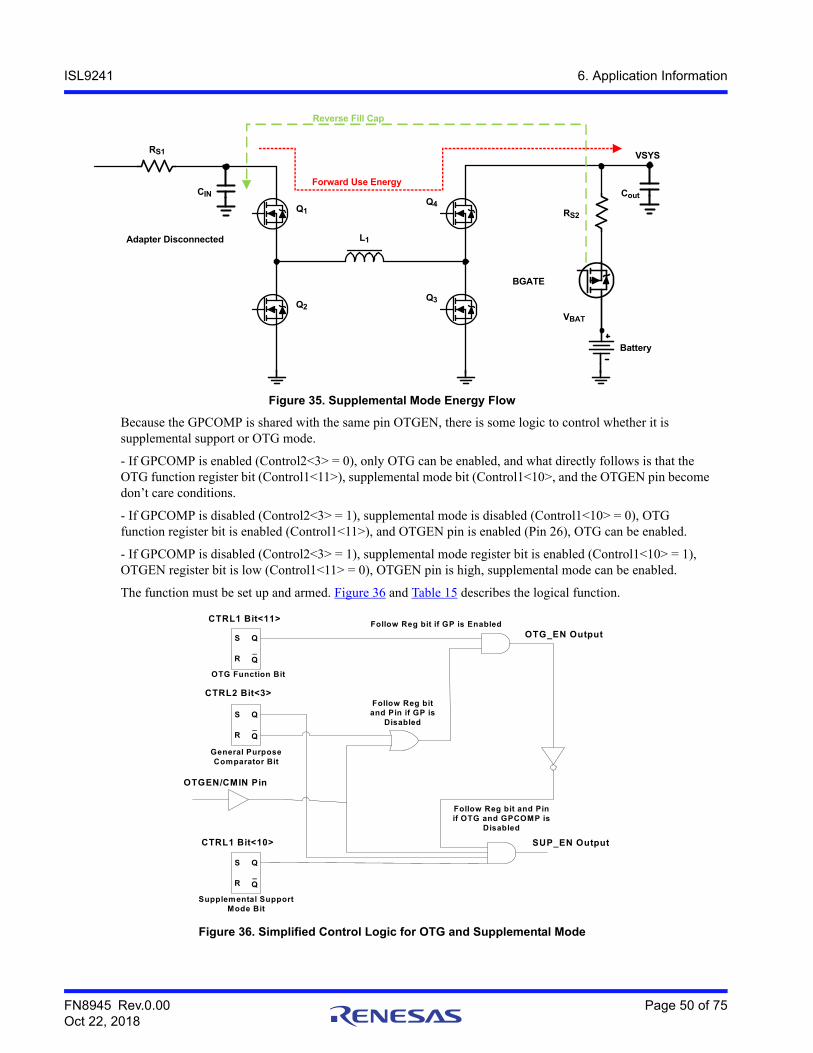
FN8945 Rev.0.00 Page 50 of 75Oct 22, 2018
ISL9241 6. Application Information
Figure 35. Supplemental Mode Energy Flow
Because the GPCOMP is shared with the same pin OTGEN, there is some logic to control whether it is supplemental support or OTG mode.
- If GPCOMP is enabled (Control2<3> = 0), only OTG can be enabled, and what directly follows is that the OTG function register bit (Control1<11>), supplemental mode bit (Control1<10>, and the OTGEN pin become don’t care conditions.
- If GPCOMP is disabled (Control2<3> = 1), supplemental mode is disabled (Control1<10> = 0), OTG function register bit is enabled (Control1<11>), and OTGEN pin is enabled (Pin 26), OTG can be enabled.
- If GPCOMP is disabled (Control2<3> = 1), supplemental mode register bit is enabled (Control1<10> = 1), OTGEN register bit is low (Control1<11> = 0), OTGEN pin is high, supplemental mode can be enabled.
The function must be set up and armed. Figure 36 and Table 15 describes the logical function.
Figure 36. Simplified Control Logic for OTG and Supplemental Mode
Q1
Q3Q2
Q4
VSYS
Battery
L1
RS1
RS2
Adapter Disconnected
BGATE
VBAT
Reverse Fill Cap
Forward Use EnergyCoutCIN
OTG_EN Output
SUP_EN Output
CTRL1 Bit<11>
CTRL1 Bit<10>
CTRL2 Bit<3>
OTGEN/CMIN Pin
R
S Q
_Q
R
S Q
_Q
R
S Q
_Q
Follow Reg bit if GP is Enabled
Follow Reg bit and Pin if GP is
Disabled
Follow Reg bit and Pin if OTG and GPCOMP is
Disabled
Supplemental Support Mode Bit
OTG Function Bit
General Purpose Comparator Bit
FN8945 Rev.0.00 Page 51 of 75Oct 22, 2018
ISL9241 6. Application Information
6.5 Monitoring
6.5.1 Current MonitorThe ISL9241 provides an adapter current monitor/OTG current monitor or a battery charging current monitor/battery discharging current monitor through the AMON/BMON pin. The AMON output voltage is 18x (CSIP - CSIN) and 18x (CSIN - CSIP) voltage, and the BMON output voltage is 18x (CSON - CSOP) and 36x (CSOP - CSON) voltage.
The AMON and BMON functions can be enabled or disabled through SMBus Control1 register Bit<5>, AMON or BMON can be selected through SMBus Control1 register Bit<4>, and AMON/BMON direction can be configured through SMBus Control3 register Bit<3>.
6.5.2 PSYS MonitorThe ISL9241 PSYS pin provides a measure of the instantaneous power consumption of the entire platform. The PSYS pin outputs a current source described by Equation 1.
KPSYS is based on current-sensing resistor Rs1 = 20mΩ and Rs2 = 10mΩ. VADP (CSIN) is the adapter voltage in Volts, IADP is the adapter current in Amperes, VBAT (CSON) is the battery voltage, and IBAT is the battery discharging current. When the battery is discharging, IBAT is a positive value; when the battery is being charged, IBAT is a negative value. The battery voltage VBAT is detected through the CSON pin to maximize the power monitor accuracy in NVDC configuration Trickle Charge mode.
The Rs1 to Rs2 ratio must be 2:1 for a valid power calculation to occur. If the resistance values are higher (or lower) than the suggested values mentioned previously, KPSYS is proportionally higher (or lower). As an example, if Rs1 = 10mΩ and Rs2 = 5mΩ, the output current is half that above for the same power. Optionally, the Rs1 to Rs2 ratio can be 1:1 for a valid power calculation to occur by setting Control4 Bit<11>. If the PSYS information is not needed, then any Rs1:Rs2 ratio is acceptable.
The PSYS gain can be configured through SMBus Control3 register Bit<9:8>. The default PSYS gain is set on VDD POR and three other settings for PSYS gain are available (see Table 6 on page 34). This gain scaling selection allows a range of power to be sensed on PSYS. The default setting is good for 60W systems, and the
Table 15. Control Logic Truth Table for OTG and Supplemental Mode
Inputs Outputs
External Pin OTGEN/CMIN
CTRL1 Bit<10>Supplemental Mode
CTRL2 Bit<3> GP Comparator
CTRL1 Bit<11>OTG Function Logic Control Signal Logic Control Signal
1 - SUP0 - OTG
1 - Disable0 - Enable
1 -Enable0 - Disable
OTG mode(OTG_EN)
Supplemental mode (SUP_EN)
0 1 1 0 0 0
0 1 1 1 1 0
0 0 1 0 0 0
0 0 1 1 1 0
1 1 1 0 0 1
1 1 1 1 1 0
1 0 1 0 1 0
1 0 1 1 1 0
x x 0 0 0 0
x x 0 1 1 0
(EQ. 1) IPSYS KPSYS VADP IADP VBAT IBAT+ Offset+=
FN8945 Rev.0.00 Page 52 of 75Oct 22, 2018
ISL9241 6. Application Information
lowest (00) setting is good for 200W systems. It may be beneficial to change this gain based on the operating condition to achieve the best accuracy.
The PSYS information includes the power loss of the charger circuit and the actual power delivered to the system. Resistor RPSYS connected between the PSYS pin and GND converts the PSYS information from current to voltage.
The PSYS function can be enabled or disabled through SMBus Control1 register Bit<3> as shown in Table 4 on page 31. Enabling the PSYS function increases the ISL9241 IC current consumption.
6.5.3 PROCHOT#PROCHOT# is an open drain output used to support IMVP protocols. On systems that do not need IMVP this pin can be used as an additional interrupt pin.
In Autonomous Charging mode, the ISL9241 starts to charge the battery with the programmed value (REG0x14h). The PROCHOT# pin behaves as Autonomous Charging mode indication pin and is pulled down to GND while charging.
6.5.3.1 Setting PROCHOT# Threshold for Adapter Overcurrent ConditionTo set the PROCHOT# assertion threshold for adapter overcurrent conditions, write a 16-bit ACProchot# command to register address 0x47H using the Write-word protocol shown in Table 31 on page 25 and the data format shown in Table 2 on page 29. By using the recommended current sense resistor values, the register’s LSB always translates to 128mA of adapter current. The ACProchot# register accepts any current command; however, only the valid register bits are written to the register, and the maximum value is clamped at 6400mA for Rs1 = 20mΩ.
After POR, the ACProchot# register is reset to 0x0C00H. The ACProchot# register can be read back to verify its content.
If the adapter current exceeds the ACProchot# register setting, the PROCHOT# signal asserts after the debounce time programmed by the Control2 register Bit<10:9> and latches on for a minimum time programmed by Control2 register Bit<8:6>.
6.5.3.2 Setting PROCHOT# Threshold for Battery Over Discharging Current Condition
To set the PROCHOT# signal assertion threshold for battery over discharging current condition, write a 16-bit DCProchot# command to register address 0x48H using the Write-word protocol shown in Figure 31 on page 25. By using the recommended current sense resistor values, the register’s LSB always translates to 256mA of adapter current. The DCProchot# register accepts any current command; however, only the valid register bits are written to the register, and the maximum value is clamped at 12.8A for Rs2 = 10mΩ.
After POR, the DCProchot# register is reset to 0x1000H. The DCProchot# register can be read back to verify its content.
If the battery discharging current exceeds the DCProchot# register setting, the PROCHOT# signal asserts after the debounce time programmed by the Control2 register Bit<10:9> and latches on for a minimum time programmed by Control2 register Bit<8:6>.
In Battery Only and Low Power mode, the DCProchot# threshold is set by Control0 register Bit<4:3>.
In Battery Only mode, the DCProchot# function using the DAC (0x48H) works only when PSYS is enabled, because enabling PSYS activates the internal comparator reference. The Information1 register Bit<15> indicates whether the internal comparator reference is active. When the adapter is present, the internal comparator reference is always active.
FN8945 Rev.0.00 Page 53 of 75Oct 22, 2018
ISL9241 6. Application Information
6.5.3.3 Low_VSYS PROCHOT#Low_VSYS is configured using Control1 Bits<2:0> (Table 4 on page 31); there are eight settings available.
6.5.3.4 Supplemental Low_VSYS PROCHOT#During supplemental mode, the Low_VSYS is configured to activate the forward mode using the energy stored in the input capacitance. See “Supplemental Power Support Mode” on page 49 for more information about how supplemental power affects PROCHOT#.
Low_VSYS is set using Control1 Bits<2:0> (Table 4 on page 31). Eight settings are available.
6.5.3.5 Other PROCHOT# ConfigurationControl4 Bits<7:4> (see Table 7 on page 35) can be used to configure the PROCHOT# to be asserted for the following triggers: OTG Current, BATGONE, ACOK, or General Purpose Comparator.
6.5.3.6 Setting PROCHOT# Debounce Time and Duration TimeControl2 register Bit<10:9> (see Table 5 on page 33) configures the PROCHOT# signal debounce time before its assertion for ACProchot# and DCProchot#.
The low system (VSYS_LOW) voltage PROCHOT# has a fixed debounce time of 10µs; but when Supplemental mode is enabled, the signal is shortened to approximately 2µs.
Control2 register Bit<8:6> configures the minimum duration of the PROCHOT# signal when asserted for VSYS_LOW, ACPROCHOT#, and DCPROCHOT#.
For the ACOK and BATGONE, Control4 Bits<3:2> (see Table 7 on page 35) can configure the debounce time before PROCHOT# is asserted.
6.5.3.7 Setting PROCHOT# Clear and Latch Control BitsControl4 Bit<1> Table 7 on page 35 can be used to configure the PROCHOT# to latch and hold its state. This is helpful as an interrupt flag to allow the system to figure out what happened. If this bit is set then the Control4 Bit<1> Table 7 on page 35 must be used to clear the asserted PROCHOT#.
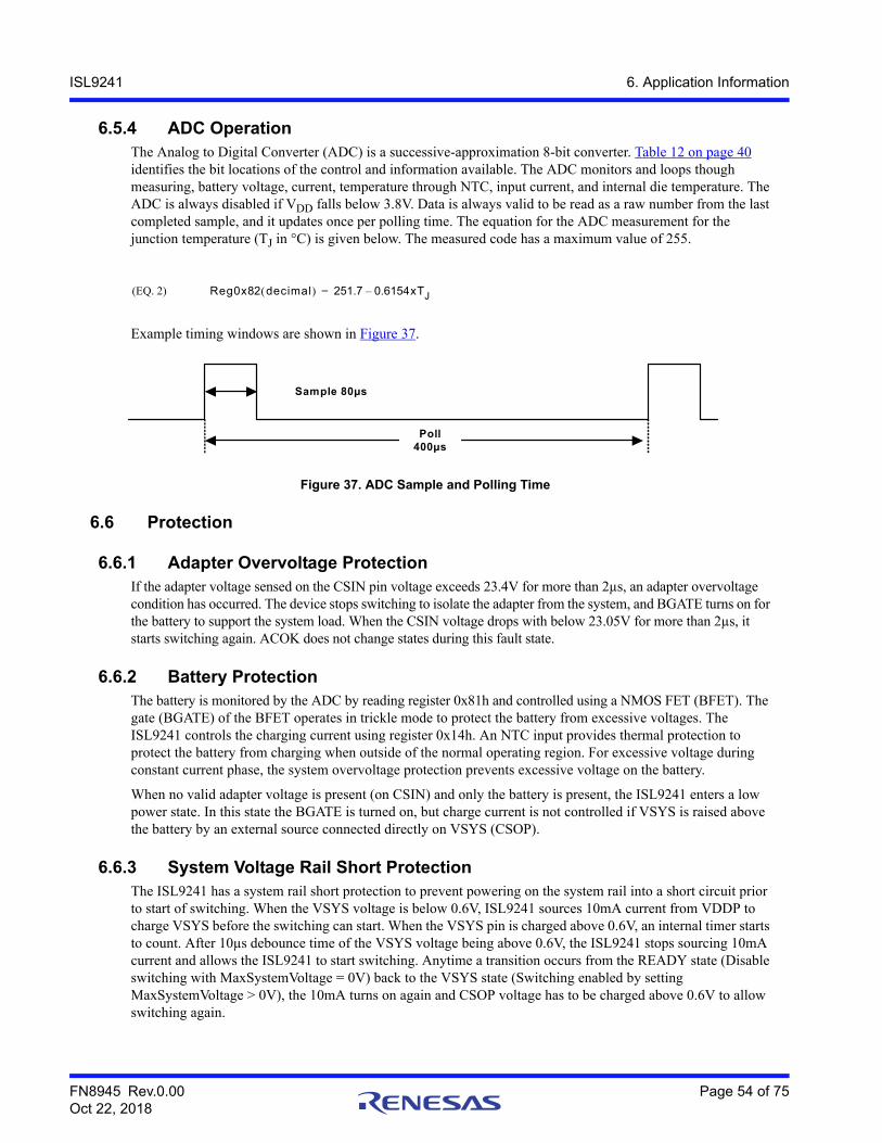
FN8945 Rev.0.00 Page 54 of 75Oct 22, 2018
ISL9241 6. Application Information
6.5.4 ADC OperationThe Analog to Digital Converter (ADC) is a successive-approximation 8-bit converter. Table 12 on page 40 identifies the bit locations of the control and information available. The ADC monitors and loops though measuring, battery voltage, current, temperature through NTC, input current, and internal die temperature. The ADC is always disabled if VDD falls below 3.8V. Data is always valid to be read as a raw number from the last completed sample, and it updates once per polling time. The equation for the ADC measurement for the junction temperature (TJ in °C) is given below. The measured code has a maximum value of 255.
Example timing windows are shown in Figure 37.
6.6 Protection
6.6.1 Adapter Overvoltage ProtectionIf the adapter voltage sensed on the CSIN pin voltage exceeds 23.4V for more than 2µs, an adapter overvoltage condition has occurred. The device stops switching to isolate the adapter from the system, and BGATE turns on for the battery to support the system load. When the CSIN voltage drops with below 23.05V for more than 2µs, it starts switching again. ACOK does not change states during this fault state.
6.6.2 Battery ProtectionThe battery is monitored by the ADC by reading register 0x81h and controlled using a NMOS FET (BFET). The gate (BGATE) of the BFET operates in trickle mode to protect the battery from excessive voltages. The ISL9241 controls the charging current using register 0x14h. An NTC input provides thermal protection to protect the battery from charging when outside of the normal operating region. For excessive voltage during constant current phase, the system overvoltage protection prevents excessive voltage on the battery.
When no valid adapter voltage is present (on CSIN) and only the battery is present, the ISL9241 enters a low power state. In this state the BGATE is turned on, but charge current is not controlled if VSYS is raised above the battery by an external source connected directly on VSYS (CSOP).
6.6.3 System Voltage Rail Short ProtectionThe ISL9241 has a system rail short protection to prevent powering on the system rail into a short circuit prior to start of switching. When the VSYS voltage is below 0.6V, ISL9241 sources 10mA current from VDDP to charge VSYS before the switching can start. When the VSYS pin is charged above 0.6V, an internal timer starts to count. After 10µs debounce time of the VSYS voltage being above 0.6V, the ISL9241 stops sourcing 10mA current and allows the ISL9241 to start switching. Anytime a transition occurs from the READY state (Disable switching with MaxSystemVoltage = 0V) back to the VSYS state (Switching enabled by setting MaxSystemVoltage > 0V), the 10mA turns on again and CSOP voltage has to be charged above 0.6V to allow switching again.
Figure 37. ADC Sample and Polling Time
(EQ. 2) Reg0x82 decimal 251.7 0.6154xTJ–=
Sample 80µs
Poll400µs
FN8945 Rev.0.00 Page 55 of 75Oct 22, 2018
ISL9241 6. Application Information
6.6.4 System Voltage Overvoltage ProtectionThe ISL9241 provides system rail overvoltage protection. If the system voltage VSYS is 800mV higher than the MaxSystemVoltage register set value, it declares the system overvoltage and stops switching. It resumes switching without debounce when VSYS drops 400mV below the system overvoltage threshold.
6.6.5 Way Overcurrent Protection (WOCP)If the system bus is shorted, either a MOSFET short or an inductor short, the input current could be high. The ISL9241 includes input overcurrent protection to turn off the BYPSG and stop switching.
The ISL9241 provides adapter current and battery discharging current Way Overcurrent Protection (WOCP) function against the MOSFET shorts, system bus shorts, and inductor shorts. The ISL9241 monitors the CSIP - CSIN voltage and CSON - CSOP voltage, and compares them with the WOCP threshold (12A for adapter current and 20A for battery discharge current).
When the WOC comparator is tripped, the ISL9241 increments a timer every 10µs. Whenever the timer reaches 7 counts, the charger deasserts ACOK, and stops switching immediately. The timer is reset every 50ms. After the 1.3s or 150ms debounce time set by Control2 register Bit<11>, it goes through the start-up sequence to retry.
The WOCP function can be disabled through Control4 register Bit<9>.
6.6.6 Over-Temperature ProtectionThe ISL9241 stops switching for self protection when the junction temperature exceeds +140°C.
When the temperature falls below +120°C for 100µs and after the 1.3s or 150ms delay, the ISL9241 starts switching.
Internal die temperature can be monitored using the ADC, and firmware can update parameters to avoid thermal shutdown.
In addition to the internal die temperature, you can use a thermistor for an NTC on the BATGONE pin to control charging in accordance to the JEITA profiles. Refer to “BATGONE” on page 45 for more details.
6.7 Additional Features
6.7.1 Stand-Alone ComparatorThe ISL9241 includes a general purpose stand-alone comparator. The OTGEN/CMIN pin is the comparator input. The internal comparator reference is connected to the inverting input of the comparator and is configured by Control2 register Bit<4> as 1.2V or 2V (Table 5 on page 33). The comparator output is the CMOUT/INT# pin, and the output polarity when the comparator is tripped can be configured through the SMBus register bit.
When Control2 register Bit<2> = 0 for normal comparator output polarity and if CMIN > Reference, CMOUT = High; if CMIN < Reference, CMOUT = Low.
When Control2 register Bit<2> = 1 for inversed comparator output polarity and if CMIN > Reference, CMOUT = Low; if CMIN < Reference, CMOUT = High.
By default in Battery Only mode, the stand-alone comparator is enabled. This comparator can be enabled/disabled in Battery Only mode using Control4 register Bit<12> (Table 7 on page 35); however, the reference is set to 1.2V. Control 2 <3> should also be enabled to enable the General purpose comparator in Battery only mode.
The general purpose comparator and INT# share the same pin, so either of them can pull the pin low if interrupts and GPCOMP are enabled. If all interrupts are disabled, the CMOUT/INT# pin shows the output of the GPCOMP. If GPCOMP is disabled, the pin indicates interrupt status only.
Figure 38 shows the Interrupt and the stand-alone comparator implementation.
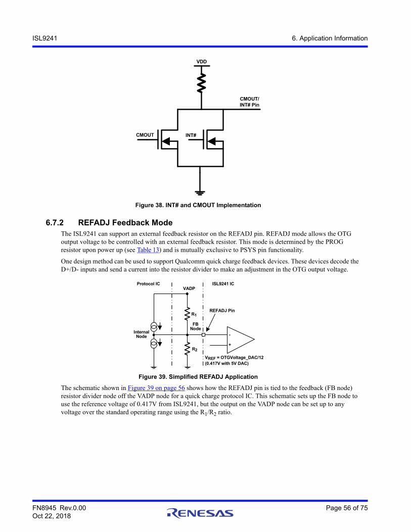
FN8945 Rev.0.00 Page 56 of 75Oct 22, 2018
ISL9241 6. Application Information
Figure 38. INT# and CMOUT Implementation
6.7.2 REFADJ Feedback ModeThe ISL9241 can support an external feedback resistor on the REFADJ pin. REFADJ mode allows the OTG output voltage to be controlled with an external feedback resistor. This mode is determined by the PROG resistor upon power up (see Table 13) and is mutually exclusive to PSYS pin functionality.
One design method can be used to support Qualcomm quick charge feedback devices. These devices decode the D+/D- inputs and send a current into the resistor divider to make an adjustment in the OTG output voltage.
Figure 39. Simplified REFADJ Application
The schematic shown in Figure 39 on page 56 shows how the REFADJ pin is tied to the feedback (FB node) resistor divider node off the VADP node for a quick charge protocol IC. This schematic sets up the FB node to use the reference voltage of 0.417V from ISL9241, but the output on the VADP node can be set up to any voltage over the standard operating range using the R1/R2 ratio.
VDD
CMOUT/INT# Pin
CMOUT INT#
REFADJ Pin
R2
VADP
R1
VREF = OTGVoltage_DAC/12 (0.417V with 5V DAC)
Internal Node
Protocol IC ISL9241 IC
+
-
FB Node
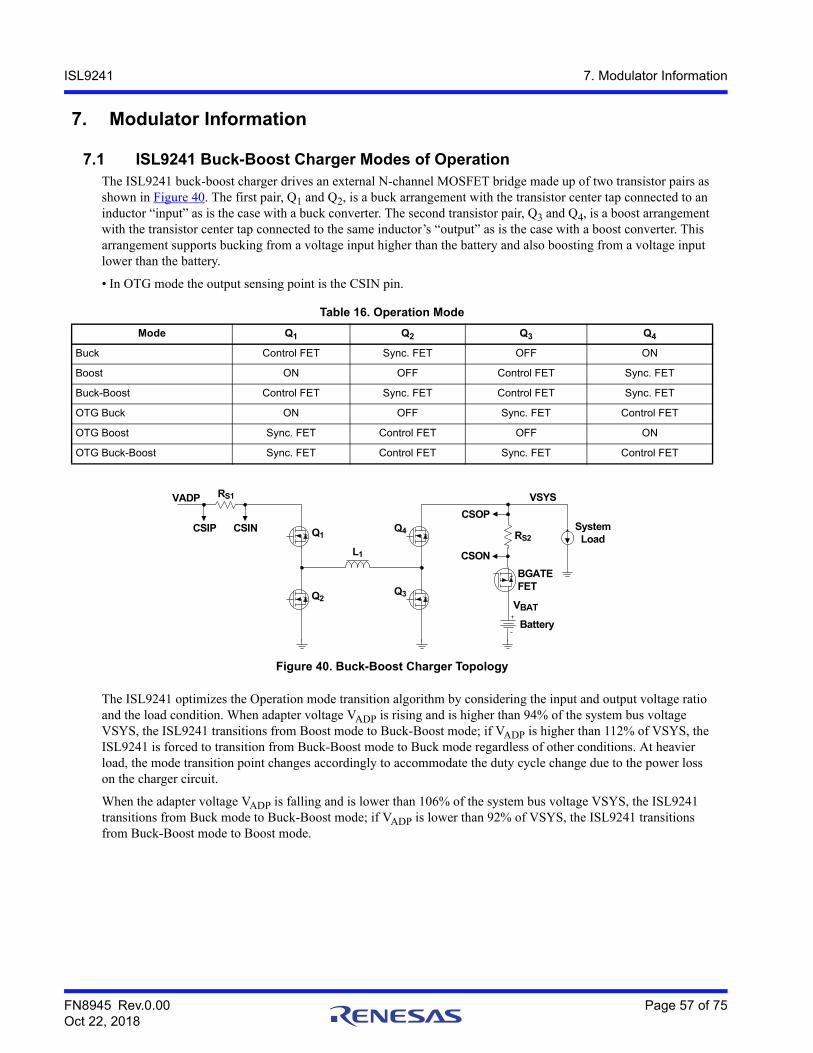
FN8945 Rev.0.00 Page 57 of 75Oct 22, 2018
ISL9241 7. Modulator Information
7. Modulator Information
7.1 ISL9241 Buck-Boost Charger Modes of OperationThe ISL9241 buck-boost charger drives an external N-channel MOSFET bridge made up of two transistor pairs as shown in Figure 40. The first pair, Q1 and Q2, is a buck arrangement with the transistor center tap connected to an inductor “input” as is the case with a buck converter. The second transistor pair, Q3 and Q4, is a boost arrangement with the transistor center tap connected to the same inductor’s “output” as is the case with a boost converter. This arrangement supports bucking from a voltage input higher than the battery and also boosting from a voltage input lower than the battery.
• In OTG mode the output sensing point is the CSIN pin.
The ISL9241 optimizes the Operation mode transition algorithm by considering the input and output voltage ratio and the load condition. When adapter voltage VADP is rising and is higher than 94% of the system bus voltage VSYS, the ISL9241 transitions from Boost mode to Buck-Boost mode; if VADP is higher than 112% of VSYS, the ISL9241 is forced to transition from Buck-Boost mode to Buck mode regardless of other conditions. At heavier load, the mode transition point changes accordingly to accommodate the duty cycle change due to the power loss on the charger circuit.
When the adapter voltage VADP is falling and is lower than 106% of the system bus voltage VSYS, the ISL9241 transitions from Buck mode to Buck-Boost mode; if VADP is lower than 92% of VSYS, the ISL9241 transitions from Buck-Boost mode to Boost mode.
Table 16. Operation Mode
Mode Q1 Q2 Q3 Q4
Buck Control FET Sync. FET OFF ON
Boost ON OFF Control FET Sync. FET
Buck-Boost Control FET Sync. FET Control FET Sync. FET
OTG Buck ON OFF Sync. FET Control FET
OTG Boost Sync. FET Control FET OFF ON
OTG Buck-Boost Sync. FET Control FET Sync. FET Control FET
Figure 40. Buck-Boost Charger Topology
CSIN
CSON
CSIPCSOP
Q1
Q3Q2
Q4
VSYS
Battery
SystemLoad
L1
RS1
RS2
VADP
BGATEFET
VBAT
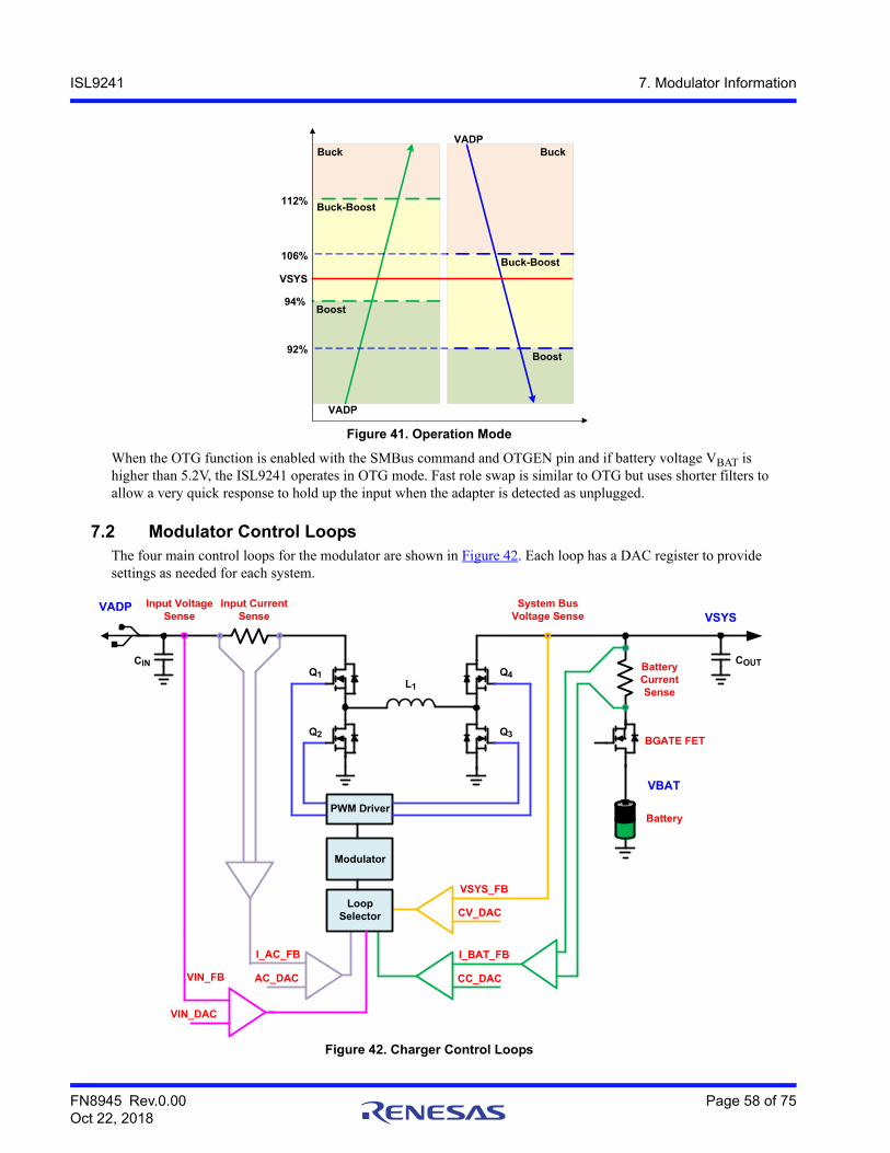
FN8945 Rev.0.00 Page 58 of 75Oct 22, 2018
ISL9241 7. Modulator Information
Figure 41. Operation Mode
When the OTG function is enabled with the SMBus command and OTGEN pin and if battery voltage VBAT is higher than 5.2V, the ISL9241 operates in OTG mode. Fast role swap is similar to OTG but uses shorter filters to allow a very quick response to hold up the input when the adapter is detected as unplugged.
7.2 Modulator Control LoopsThe four main control loops for the modulator are shown in Figure 42. Each loop has a DAC register to provide settings as needed for each system.
Figure 42. Charger Control Loops
94%
112%
106%
92%
VSYS
VADP
VADP
Buck-Boost
Buck
Boost
Boost
Buck-Boost
Buck
COUT
L1
Input Current Sense
Battery Current Sense
VSYS
PWM Driver Battery
Q1
Q2
Q4
Q3
AC_DAC
I_BAT_FB
CC_DAC
I_AC_FB
VSYS_FB
CV_DACLoop
Selector
Modulator
System Bus Voltage Sense
VIN_DAC
VIN_FB
Input Voltage Sense
BGATE FET
VBAT
VADP
CIN
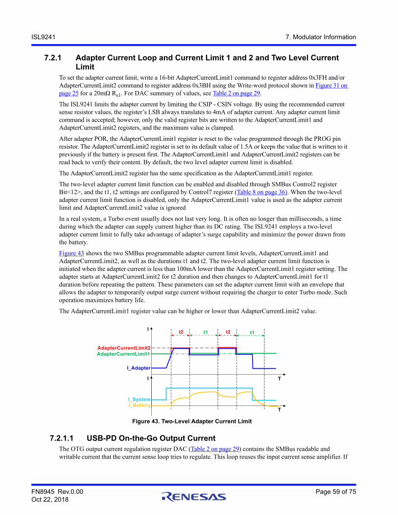
FN8945 Rev.0.00 Page 59 of 75Oct 22, 2018
ISL9241 7. Modulator Information
7.2.1 Adapter Current Loop and Current Limit 1 and 2 and Two Level Current Limit
To set the adapter current limit, write a 16-bit AdapterCurrentLimit1 command to register address 0x3FH and/or AdapterCurrentLimit2 command to register address 0x3BH using the Write-word protocol shown in Figure 31 on page 25 for a 20mΩ Rs1. For DAC summary of values, see Table 2 on page 29.
The ISL9241 limits the adapter current by limiting the CSIP - CSIN voltage. By using the recommended current sense resistor values, the register’s LSB always translates to 4mA of adapter current. Any adapter current limit command is accepted; however, only the valid register bits are written to the AdapterCurrentLimit1 and AdapterCurrentLimit2 registers, and the maximum value is clamped.
After adapter POR, the AdapterCurrentLimit1 register is reset to the value programmed through the PROG pin resistor. The AdapterCurrentLimit2 register is set to its default value of 1.5A or keeps the value that is written to it previously if the battery is present first. The AdapterCurrentLimit1 and AdapterCurrentLimit2 registers can be read back to verify their content. By default, the two level adapter current limit is disabled.
The AdapterCurrentLimit2 register has the same specification as the AdapterCurrentLimit1 register.
The two-level adapter current limit function can be enabled and disabled through SMBus Control2 register Bit<12>, and the t1, t2 settings are configured by Control7 register (Table 8 on page 36). When the two-level adapter current limit function is disabled, only the AdapterCurrentLimit1 value is used as the adapter current limit and AdapterCurrentLimit2 value is ignored
In a real system, a Turbo event usually does not last very long. It is often no longer than milliseconds, a time during which the adapter can supply current higher than its DC rating. The ISL9241 employs a two-level adapter current limit to fully take advantage of adapter’s surge capability and minimize the power drawn from the battery.
Figure 43 shows the two SMBus programmable adapter current limit levels, AdapterCurrentLimit1 and AdapterCurrentLimit2, as well as the durations t1 and t2. The two-level adapter current limit function is initiated when the adapter current is less than 100mA lower than the AdapterCurrentLimit1 register setting. The adapter starts at AdapterCurrentLimit2 for t2 duration and then changes to AdapterCurrentLimit1 for t1 duration before repeating the pattern. These parameters can set the adapter current limit with an envelope that allows the adapter to temporarily output surge current without requiring the charger to enter Turbo mode. Such operation maximizes battery life.
The AdapterCurrentLimit1 register value can be higher or lower than AdapterCurrentLimit2 value.
Figure 43. Two-Level Adapter Current Limit
7.2.1.1 USB-PD On-the-Go Output CurrentThe OTG output current regulation register DAC (Table 2 on page 29) contains the SMBus readable and writable current that the current sense loop tries to regulate. This loop reuses the input current sense amplifier. If
AdapterCurrentLimit1
I_Adapter
I_SystemI_Battery
t2 t1
T
T
I
I
AdapterCurrentLimit2
t2 t1
FN8945 Rev.0.00 Page 60 of 75Oct 22, 2018
ISL9241 7. Modulator Information
USB-PD Programmable Power Supply is desired, this is the current limit loop. Note that the OTG_UV needs to be disabled (see CTRL3 Bit<15> in Table 6 on page 34).
This register accepts any current command, but only the valid register bits are written to the register. The maximum value is clamped.
7.2.2 Input Voltage Regulation Loop
7.2.2.1 Adapter Support VoltageThe input voltage regulation register DAC (Table 2 on page 29) contains the SMBus readable and writable input voltage limit at which the input voltage loop tries to regulate when the input voltage is dropping. When the ADP is browning out or weak, the input voltage can droop and the input voltage loop tries to regulate to this setting by reducing battery charging current and then system power to try to hold up the input voltage. The system voltage may start to drop if the input power is not high enough to support the system.
This register accepts any current command but only the valid register bits are written to the register The maximum value is clamped.
7.2.2.2 USB-PD On-the-Go Output VoltageThe OTG output voltage regulation register DAC (Table 2 on page 29) contains the SMBus readable and writable voltage that the voltage loop tries to regulate. This loop reuses the input voltage sense amp.
This register accepts any current command, but only the valid register bits are written to the register. The maximum value is clamped.
7.2.3 System Voltage Regulation LoopThis loop works for two different voltage settings, one MaxSystemVoltage and the other MinSystemVoltage.
If the battery is absent, or present but BGATE is turned off or not charging and then if Control0 register Bit<1> is a 0, the system voltage is regulated to the same setting as the DAC. When Control0 register Bit<1> is a 1, the system voltage is regulated to the DAC plus an offset of 384mV (Table 3 on page 30). This additional offset is useful to avoid discharging a full battery in VSYS state when there is a system load transient.
To set the maximum charging voltage or the system regulating voltage, write a 16-bit MaxSystemVoltage command to register address 0x15H using the Write-word protocol shown in Figure 31 on page 25 and the data format shown in Table 14 on page 46. A 0V command causes the ISL9241 to stop switching and enter READY state.
The ISL9241 supports trickle charging to an overly discharged battery. It can activate the trickle charging function when the battery voltage is lower than the MinSystemVoltage setting. The VBAT pin is the battery voltage sense point for Trickle Charge mode. While trickle charging the battery, the system regulation voltage is the DAC setting plus 384mV.
To enable Trickle Charging, set the MinSystemVoltage and Charge Current register to a non-zero value higher than battery voltage. To disable trickle charging, set the MinSystemVoltage and Charge Current register to 0. Refer to Table 17 on page 62 for trickle charging control logic.
The CSOP pin senses the system voltage for MaxSystemVoltage and MinSystemVoltage during trickle charging and controls the VSYS operating voltage.
7.2.4 Charging Current LoopThis loop uses the charge current DAC (see Table 15 on page 51) to set the fast charging current limit. In Trickle Charging mode, the ISL9241 regulates the trickle charging current through the buck-boost switcher. Another independent control loop controls the BGATE FET so that the system voltage is maintained at the voltage set in the MinSystemVoltage register.
FN8945 Rev.0.00 Page 61 of 75Oct 22, 2018
ISL9241 7. Modulator Information
To set it, write a 16-bit ChargeCurrentLimit command to register address 0x14H (Table 2) using the Write-word protocol shown in Figure 31 on page 25.
The ISL9241 limits the charging current by limiting the CSOP - CSON voltage, so reducing the current sense resistor value doubles the current being regulated to. By using the recommended current sense resistor values Rs1 = 20mΩand Rs2 = 10mΩ, the register’s LSB always translates to 4mA of charging current. The ChargeCurrentLimit register accepts any charging current command, but only the valid register bits are written to the register.
7.3 Buck Boost Configurable ChargerThe ISL9241 is a Buck-Boost battery charger that can support both Narrow Voltage DC (NVDC) charging or Hybrid Power Buck Boost (HPBB) charging. NVDC is the initial start up state for the ISL9241, and firmware from a controller using the I2C interface is used to change the configuration to HPBB.
The ISL9241 allows the system to be optimized for both types of configurations. For lower power systems, the NVDC mode may be appropriate and reduces system complexity. For higher power systems, the hybrid mode may be the choice to allow a smaller inductor but support higher system power with improved efficiency.
Because the system power does not pass through the inductor, hybrid power mode allows high power systems to size the inductor for just the maximum charging current or the turbo boost current. Because main power goes directly from the adapter to the system, the system efficiency improves, and the inductor is smaller saving board area. For NVDC mode configuration, the inductor has to support the full system power and needs to be a larger size, because it supports both charging and system power.
This mode allows the whole switch circuit to be bypassed only when the ADP is greater than the battery voltage. It connects the ADP to the VSYS through two NFETs using an internal charge pump for the gate drive. This mode is primarily controlled by firmware to ensure flexibility and has only fault protections for safety. Ensure that ADP > VBAT either by guaranteeing that ADP > VBAT or enabling the VIN > VOUT bypass comparator (Control0 Bit<5> (Table 3 on page 30) to automatically turn off the BYPSG gate.
NGATE turning on after exit Bypass mode should wait until discharge current or VSYS ≈ VBAT.
OTG and Fast role swap must not be allowed while in Bypass mode, and firmware must prevent the toggling of the OTGEN pin. Bypass mode must be enabled to allow reverse turbo boost operation.
Refer to the ISL9241 product information page for firmware documentation.
7.3.1 NVDC ChargerFor NVDC mode configuration, the inductor supports the full system power and the power for charging the battery. This means the inductor typically needs to be a larger size, because it supports both charging and system.
The ISL9241 automatically selects the adapter and/or the battery as the source for system power. The BGATE pin drives an N-channel MOSFET (NFET) gate that connects or disconnects the battery from the system and the switcher.
7.3.1.1 Normal ChargingFor NVDC mode configuration, the charging current is selected for the charge rate into the battery. However, the input current limit should be set for the total system plus battery charging current.
If VDD is higher than 3.8V, the ISL9241 enters Forward Buck, Forward Boost, or Forward Buck-Boost mode depending upon the adapter and system voltage VSYS duty cycle ratio. The system bus voltage is regulated at the voltage set on the MaxSystemVoltage register. If the charge current register is programmed (non-zero), the ISL9241 charges the battery either in Trickle Charging mode or Fast Charging mode as long as BATGONE is low.
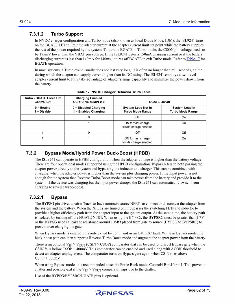
FN8945 Rev.0.00 Page 62 of 75Oct 22, 2018
ISL9241 7. Modulator Information
7.3.1.2 Turbo SupportIn NVDC charger configuration and Turbo mode (also known as Ideal Diode Mode, IDM), the ISL9241 turns on the BGATE FET to limit the adapter current at the adapter current limit set point while the battery supplies the rest of the power required by the system. To turn on BGATE in Turbo mode, the CSON pin voltage needs to be 175mV lower than the VBAT pin voltage. If the ISL9241 detects 150mA charging current or if the battery discharging current is less than 140mA for 140ms, it turns off BGATE to exit Turbo mode. Refer to Table 17 for BGATE operation.
In most systems, a Turbo event usually does not last very long. It is often no longer than milliseconds, a time during which the adapter can supply current higher than its DC rating. The ISL9241 employs a two-level adapter current limit to fully take advantage of adapter’s surge capability and minimize the power drawn from the battery.
7.3.2 Bypass Mode/Hybrid Power Buck-Boost (HPBB)The ISL9241 can operate in HPBB configuration when the adapter voltage is higher than the battery voltage. There are four operational modes supported using the HPBB configuration. Bypass refers to both passing the adapter power directly to the system and bypassing the inductor and charger. This can be combined with charging, when the adapter power is higher than the system plus charging power. If the input power is not enough for the system then Reverse Turbo-Boost mode can take power from the battery and provide it to the system. If the device was charging but the input power droops, the ISL9241 can automatically switch from charging to reverse turbo-boost.
7.3.2.1 BypassThe BYPSG pin drives a pair of back-to-back common source NFETs to connect or disconnect the adapter from the system and the battery. When the NFETs are turned on, it bypasses the switching FETs and inductor to provide a higher efficiency path from the adapter input to the system output. At the same time, the battery path is isolated by turning off the NGATE NFET. When using the BYPSG, the BYPSRC must be greater than 2.7V, or the BYPSG needs a leakage resistance around 10MΩ placed from gate to source (BYPSG to BYPSRC) to prevent over charging the gate.
When Bypass mode is entered, it is only exited by command or an OVP/OC fault. While in Bypass mode, the buck-boost path can then support a Reverse Turbo Boost mode and augment the adapter power from the battery.
There is an optional VIN > VOUT (CSIN > CSOP) comparator that can be used to turn off Bypass gate when the CSIN falls below CSOP + 400mV. This comparator can be enabled and used along with ACOK threshold to detect an adapter unplug event. The comparator turns on Bypass gate again when CSIN rises above CSOP + 800mV.
When using Bypass mode, it is recommended to set the Force Buck mode, Control4 Bit<10> = 1. This prevents chatter and possible exit if the VIN > VOUT comparator trips due to the chatter.
Use of the BYPSG/BYPSRC/NGATE pins is optional.
Table 17. NVDC Charger Behavior Truth Table
Turbo - BGATE Force Off Control Bit
Charging EnabledCC ≠ 0; VSYSMIN ≠ 0 BGATE On/Off
0 = Enable 1 = Disable
0 = Disabled Charging1 = Enabled Charging
System Load Not InTurbo Mode Range
System Load InTurbo Mode Range
0 0 Off On
0 1 ON for fast charge;trickle charge enabled
On
1 0 Off Off
1 1 ON for fast charge;trickle charge enabled
On
FN8945 Rev.0.00 Page 63 of 75Oct 22, 2018
ISL9241 7. Modulator Information
7.3.2.2 Bypass + ChargingWhen in Bypass mode, normal battery charging is similar to the normal charging.
7.3.2.3 Reverse Turbo-Boost ModeTurbo mode refers to the scenario in which the system draws more power than the adapter’s power rating. Turbo mode prompts the need for the switcher to change from Forward mode of operation to Reverse mode of operation in order to reverse the energy flow from going into the battery from going out of the battery. This mode of operation enables the battery to help the adapter provide the required system power. Such operation has been widely used in many systems, such as “Sun mode” and “Eclipse mode” for bidirectional battery charger/discharger used on satellites with solar panels as the power source acting as the adapter (reference “A zero voltage switching bidirectional battery charger/discharger for the NASA EOS Satellite”, Dan M. Sable, Fred C. Lee and Bo H. Cho, APEC 1992 Conference Proceedings). To use HPBB charger configuration, follow the steps from the Bypass Application document.
The ISL9241 automatically selects the adapter and/or the battery as the source for system power. When the adapter power is not enough for the system as detected by the input current limit loop, the battery needs to supplement the adapter. When this occurs, the charger operates in the reverse direction taking energy from the battery to hold up the input voltage.
The Control0 register Bit<0> enables or disables the Reverse Turbo-Boost function. Refer to Table 3 on page 30 for details. Use caution when enabling reverse Turbo, as the BFET is held on and there is potential to have excessive current into the battery. Autonomous Charging must be disabled before enabling Reverse Turbo-Boost function.
In Reverse Turbo-Boost mode, the ISL9241 operates the switcher in reverse mode to pull energy from the battery and give energy to the adapter voltage rail so that the adapter current is limited at the adapter current limit set point, while the battery supplies the additional power required by the system.
7.3.2.4 Reverse Turbo Boost Mode + ChargingOnce in Bypass mode with Reverse Turbo Enabled, normal battery charging is similar to the normal charging. Unless the adapter power is not enough for the system as detected by the input current limit loop. The battery needs to supplement the adapter. When this occurs, first the charging stops, and if the power demand increases, the ISL9241 operates in the reverse direction taking energy from the battery to hold up the input voltage.
The ISL9241 automatically enters this Reverse Turbo mode when all of the following three criteria are met:
• Adapter current is within 80mA of AdapterCurrentLimit1 (or AdapterCurrentLimit2 if two-level adapter current limit function is enabled) register setting
• Battery charging current is less than 150mA
• COMP pin voltage is lower than 1.4V
Meeting these three criteria means that the ISL9241 enters Reverse Turbo mode only when it is absolutely necessary.
For example, assuming the adapter voltage is 20V, the adapter current limit is 4A (80W rating), and the ISL9241 is charging an 8V battery at a 5A rate (40W charging power). If the system load increases from 0W to 79W instantaneously, the adapter current increases from 2A to 5.95A instantaneously exceeding the 4A current limit level. However, the adapter current loop takes control and decreases the charging current to limit the adapter current at 4A, eventually providing 79W of system power and 1W of battery charging power. In this case, the ISL9241 does not need to enter Turbo mode adapter and can conserve battery energy. In the same example, if the system load increases from 0W to 81W instantaneously, the adapter current increases from 2A to 6.05A instantaneously, exceeding the 4A current limit level. The adapter current loop takes control and decreases the charging current to limit the adapter current at 4A. Therefore, the ISL9241 eventually determines that it needs to enter Turbo mode so that the adapter provides 80W, and the battery provides 1W to provide 81W to the system.
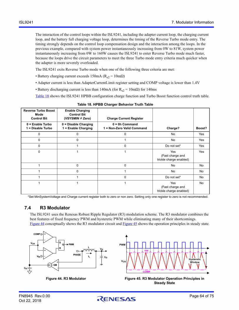
FN8945 Rev.0.00 Page 64 of 75Oct 22, 2018
ISL9241 7. Modulator Information
The interaction of the control loops within the ISL9241, including the adapter current loop, the charging current loop, and the battery full charging voltage loop, determines the timing of the Reverse Turbo mode entry. The timing strongly depends on the control loop compensation design and the interaction among the loops. In the previous example, compared with system power instantaneously increasing from 0W to 81W, system power instantaneously increasing from 0W to 160W causes the ISL9241 to enter Reverse Turbo mode much faster, because the loops drive the circuit parameters to meet the three Turbo mode entry criteria much quicker when the adapter is more severely overloaded.
The ISL9241 exits Reverse Turbo mode when one of the following three criteria are met:
• Battery charging current exceeds 150mA (Rs2 = 10mΩ)
• Adapter current is less than AdapterCurrentLimit register setting and COMP voltage is lower than 1.4V
• Battery discharging current is less than 140mA (for Rs2 = 10mΩ) for 140ms
Table 18 shows the ISL9241 HPBB configuration charge function and Turbo Boost function control truth table.
7.4 R3 ModulatorThe ISL9241 uses the Renesas Robust Ripple Regulator (R3) modulation scheme. The R3 modulator combines the best features of fixed frequency PWM and hysteretic PWM while eliminating many of their shortcomings. Figure 44 conceptually shows the R3 modulator circuit and Figure 45 shows the operation principles in steady state.
Table 18. HPBB Charger Behavior Truth Table
Reverse Turbo Boost Mode
Control Bit
Enable ChargingControl Bit
(VSYSMIN ≠ Zero) Charge Current Register
Charge? Boost?0 = Enable Turbo1 = Disable Turbo
0 = Disable Charging1 = Enable Charging
0 = 0h Command1 = Non-Zero Valid Command
0 0 0 No Yes
0 0 1 No Yes
0 1 0 Do not set* Yes
0 1 1 Yes(Fast charge and
trickle charge enabled)
Yes
1 0 0 No No
1 0 1 No No
1 1 0 Do not set* No
1 1 1 Yes(Fast charge and
trickle charge enabled)
No
*Set MinSystemVoltage and Charge current register both to zero or non zero. Setting only one register to zero is not recommended.
Figure 44. R3 Modulator Figure 45. R3 Modulator Operation Principles in Steady State
COMP
R
IL
GM
PHASE
CR
VW
SQ PWM
L
CO
VO
VCR
+
+
+
-
-
-
COMP
PWM
VCRHysteretic Window
VW
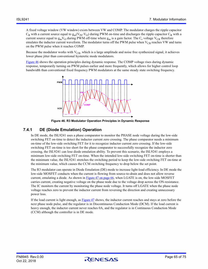
FN8945 Rev.0.00 Page 65 of 75Oct 22, 2018
ISL9241 7. Modulator Information
A fixed voltage window (VW window) exists between VW and COMP. The modulator charges the ripple capacitor CR with a current source equal to gm(VIN-VO) during PWM on-time and discharges the ripple capacitor CR with a current source equal to gmVO during PWM off-time where gm is a gain factor. The Cr voltage VCR therefore emulates the inductor current waveform. The modulator turns off the PWM pulse when VCR reaches VW and turns on the PWM pulse when it reaches COMP.
Because the modulator works with VCR, which is a large amplitude and noise free synthesized signal, it achieves lower phase jitter than conventional hysteretic mode modulators.
Figure 46 shows the operation principles during dynamic response. The COMP voltage rises during dynamic response, temporarily turning on PWM pulses earlier and more frequently, which allows for higher control loop bandwidth than conventional fixed frequency PWM modulators at the same steady state switching frequency.
7.4.1 DE (Diode Emulation) OperationIn DE mode, the ISL9241 uses a phase comparator to monitor the PHASE node voltage during the low-side switching FET on-time to detect the inductor current zero crossing. The phase comparator needs a minimum on-time of the low-side switching FET for it to recognize inductor current zero crossing. If the low-side switching FET on-time is too short for the phase comparator to successfully recognize the inductor zero crossing, the ISL9241 can lose diode emulation ability. To prevent this scenario, the ISL9241 employs a minimum low-side switching FET on-time. When the intended low-side switching FET on-time is shorter than the minimum value, the ISL9241 stretches the switching period to keep the low-side switching FET on-time at the minimum value, which causes the CCM switching frequency to drop below the set point.
The R3 modulator can operate in Diode Emulation (DE) mode to increase light-load efficiency. In DE mode the low-side MOSFET conducts when the current is flowing from source-to-drain and does not allow reverse current, emulating a diode. As shown in Figure 47 on page 66, when LGATE is on, the low-side MOSFET carries current, creating negative voltage on the phase node due to the voltage drop across the ON-resistance. The IC monitors the current by monitoring the phase node voltage. It turns off LGATE when the phase node voltage reaches zero to prevent the inductor current from reversing the direction and creating unnecessary power loss.
If the load current is light enough, as Figure 47 shows, the inductor current reaches and stays at zero before the next phase node pulse, and the regulator is in Discontinuous Conduction Mode (DCM). If the load current is heavy enough, the inductor current never reaches 0A, and the regulator is in Continuous Conduction Mode (CCM) although the controller is in DE mode.
Figure 46. R3 Modulator Operation Principles in Dynamic Response
PWM
VCR
VW
COMP
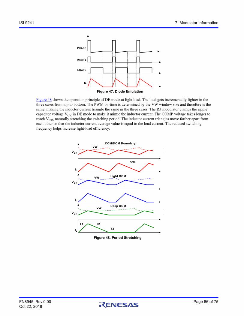
FN8945 Rev.0.00 Page 66 of 75Oct 22, 2018
ISL9241 7. Modulator Information
Figure 48 shows the operation principle of DE mode at light load. The load gets incrementally lighter in the three cases from top to bottom. The PWM on-time is determined by the VW window size and therefore is the same, making the inductor current triangle the same in the three cases. The R3 modulator clamps the ripple capacitor voltage VCR in DE mode to make it mimic the inductor current. The COMP voltage takes longer to reach VCR, naturally stretching the switching period. The inductor current triangles move farther apart from each other so that the inductor current average value is equal to the load current. The reduced switching frequency helps increase light-load efficiency.
Figure 47. Diode Emulation
Figure 48. Period Stretching
UGATE
PHASE
IL
LGATE
IL
IL
VCR
IL
VCR
VCR
VWCCM/DCM Boundary
Light DCM
Deep DCM
VW
VW
T1 T2
T3
CCM
FN8945 Rev.0.00 Page 67 of 75Oct 22, 2018
ISL9241 8. Design Guide
8. Design GuideThis design guide provides a high-level explanation of the steps necessary to design a single-phase power converter. It is assumed that the reader is familiar with many of the basic skills and techniques referenced in the following section. In addition to this, complete reference designs that include schematics, bills of materials, and example board layouts are provided.
8.1 Selecting the Sense ResistorsSense resistors are the easiest and most flexible method of monitoring/controlling current in the battery charge, discharge path, or the adapter input/output current. Most of the electrical specifications in this data sheet used Rs1 = 20mΩ and Rs2 = 10mΩ. However, any value can be selected because it is the voltage across the CSIN/CSIP and CSON/CSOP pins that are used for the control loops.
A sense resistor can introduce significant voltage drop and power loss to the load. In an application with high current requirements, the sense resistors require the use of low value sense resistor or a parallel combination of multiple sense resistors to support the higher power.
Appropriate scaling of the current values should be based on the voltage across the CSIN/CSIP and CSON/CSOP.
For example, if DAC is set for 2A at R = 20mΩ, Vsx = 40mV; with R = 10mΩ, which is half the previous value, the DAC setting ends up being doubled to 4A to preserve Vsx = 40mV.
8.1.1 Adapter Sense ResistorThe adapter sense resistor (Rs1) controls the current being pulled from an adapter when in forward mode, and senses the maximum current for ACProchot#. In Reverse mode, the sense resistor regulates the output current for OTG mode.
8.1.2 Battery Sense ResistorThe battery sense resistor (Rs2) controls the battery charging current when in Forward mode. In Reverse mode, the sense resistor senses the battery discharging current for DCProchot#.
8.2 Selecting the LC Output FilterThe duty cycle of an ideal buck converter in CCM is a function of the input and the output voltage. This relationship is written by Equation 3:
The output inductor peak-to-peak ripple current is written by Equation 4:
A typical step-down DC/DC converter has an IP-P of 20% to 40% of the maximum DC output load current for a practical design. The value of IP-P is selected based upon several criteria such as MOSFET switching loss, inductor core loss, and the resistive loss of the inductor winding.
The DC copper loss of the inductor can be estimated by Equation 5:
where ILOAD is the converter output DC current.
The copper loss can be significant so attention has to be given to the DCR selection. Another factor to consider when choosing the inductor is its saturation characteristics at elevated temperatures. A saturated inductor can destroy circuit components.
DVOUTVIN
---------------=(EQ. 3)
(EQ. 4) IP-P
VOUT 1 D–
fSW L--------------------------------------=
(EQ. 5) PCOPPER ILOAD2
DCR=
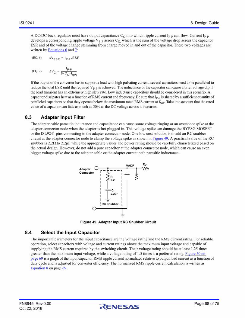
FN8945 Rev.0.00 Page 68 of 75Oct 22, 2018
ISL9241 8. Design Guide
A DC/DC buck regulator must have output capacitance CO into which ripple current IP-P can flow. Current IP-P develops a corresponding ripple voltage VP-P across CO, which is the sum of the voltage drop across the capacitor ESR and of the voltage change stemming from charge moved in and out of the capacitor. These two voltages are written by Equations 6 and 7:
If the output of the converter has to support a load with high pulsating current, several capacitors need to be paralleled to reduce the total ESR until the required VP-P is achieved. The inductance of the capacitor can cause a brief voltage dip if the load transient has an extremely high slew rate. Low inductance capacitors should be considered in this scenario. A capacitor dissipates heat as a function of RMS current and frequency. Be sure that IP-P is shared by a sufficient quantity of paralleled capacitors so that they operate below the maximum rated RMS current at fSW. Take into account that the rated value of a capacitor can fade as much as 50% as the DC voltage across it increases.
8.3 Adapter Input FilterThe adapter cable parasitic inductance and capacitance can cause some voltage ringing or an overshoot spike at the adapter connector node when the adapter is hot plugged in. This voltage spike can damage the BYPSG MOSFET or the ISL9241 pins connecting to the adapter connector node. One low cost solution is to add an RC snubber circuit at the adapter connector node to clamp the voltage spike as shown in Figure 49. A practical value of the RC snubber is 2.2Ω to 2.2µF while the appropriate values and power rating should be carefully characterized based on the actual design. However, do not add a pure capacitor at the adapter connector node, which can cause an even bigger voltage spike due to the adapter cable or the adapter current path parasitic inductance.
8.4 Select the Input CapacitorThe important parameters for the input capacitance are the voltage rating and the RMS current rating. For reliable operation, select capacitors with voltage and current ratings above the maximum input voltage and capable of supplying the RMS current required by the switching circuit. Their voltage rating should be at least 1.25 times greater than the maximum input voltage, while a voltage rating of 1.5 times is a preferred rating. Figure 50 on page 69 is a graph of the input capacitor RMS ripple current normalized relative to output load current as a function of duty cycle and is adjusted for converter efficiency. The normalized RMS ripple current calculation is written as Equation 8 on page 69.
Figure 49. Adapter Input RC Snubber Circuit
VESR IP-P E SR=(EQ. 6)
VC
IP-P8 CO f
SW
-----------------------------=(EQ. 7)
AdapterConnector
Ri
Ci
2.2
2.2µF
RC Snubber
VADP Rs1
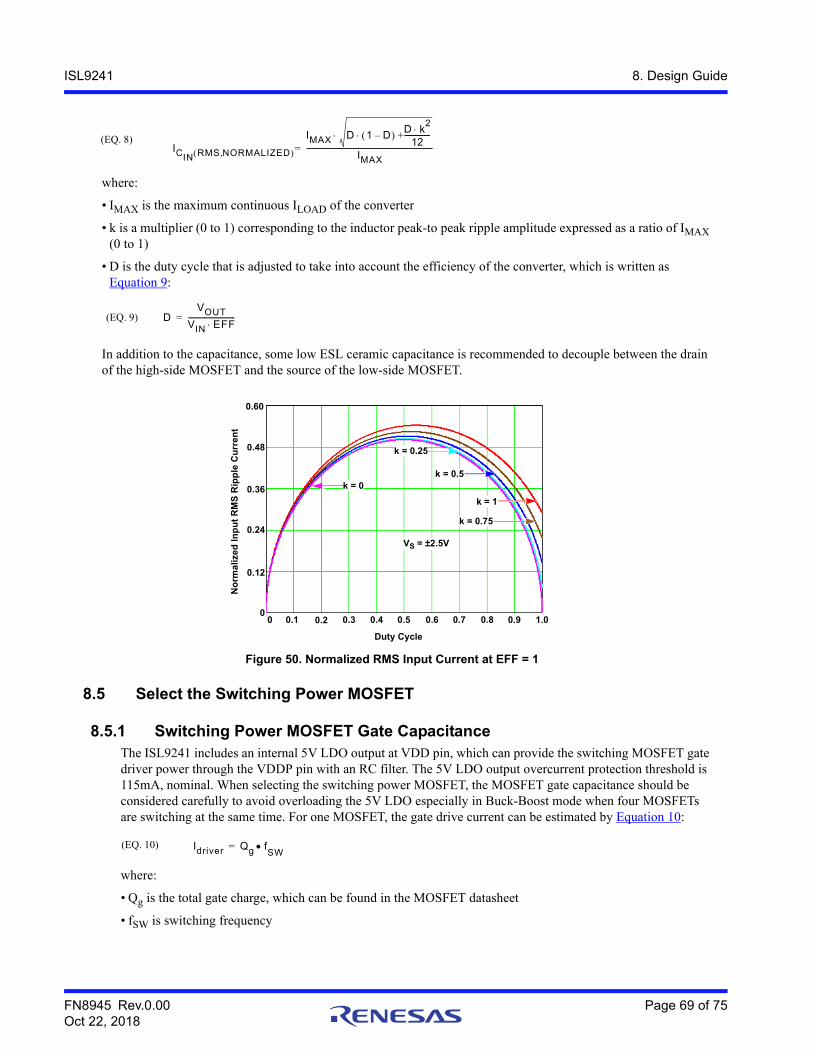
FN8945 Rev.0.00 Page 69 of 75Oct 22, 2018
ISL9241 8. Design Guide
where:
• IMAX is the maximum continuous ILOAD of the converter
• k is a multiplier (0 to 1) corresponding to the inductor peak-to peak ripple amplitude expressed as a ratio of IMAX (0 to 1)
• D is the duty cycle that is adjusted to take into account the efficiency of the converter, which is written as Equation 9:
In addition to the capacitance, some low ESL ceramic capacitance is recommended to decouple between the drain of the high-side MOSFET and the source of the low-side MOSFET.
Figure 50. Normalized RMS Input Current at EFF = 1
8.5 Select the Switching Power MOSFET
8.5.1 Switching Power MOSFET Gate CapacitanceThe ISL9241 includes an internal 5V LDO output at VDD pin, which can provide the switching MOSFET gate driver power through the VDDP pin with an RC filter. The 5V LDO output overcurrent protection threshold is 115mA, nominal. When selecting the switching power MOSFET, the MOSFET gate capacitance should be considered carefully to avoid overloading the 5V LDO especially in Buck-Boost mode when four MOSFETs are switching at the same time. For one MOSFET, the gate drive current can be estimated by Equation 10:
where:
• Qg is the total gate charge, which can be found in the MOSFET datasheet
• fSW is switching frequency
(EQ. 8)ICIN RMS NORMALIZED,
IMAX D 1 D– D k2
12--------------+
IMAX-----------------------------------------------------------------------=
DVOUT
VIN EFF--------------------------=(EQ. 9)
No
rmal
ized
Inp
ut
RM
S R
ipp
le C
urr
ent
Duty Cycle
0 0.1 0.2 0.3 0.4 0.6 0.7 0.8 0.9 1.00.50
0.12
0.24
0.36
0.48
0.60
k = 0.75
k = 0.5
k = 0.25
k = 0
VS = ±2.5V
k = 1
Idriver Qg fSW
=(EQ. 10)
FN8945 Rev.0.00 Page 70 of 75Oct 22, 2018
ISL9241 8. Design Guide
8.5.2 Switching Power MOSFET Power Typically, a MOSFET cannot tolerate even brief excursions beyond its maximum drain-to-source voltage rating. The MOSFETs used in the power stage of the converter should have a maximum VDS rating that exceeds the sum of the upper voltage tolerance of the input power source and the voltage spike that occurs when the MOSFET switches off.
Several power MOSFETs are readily available that are optimized for DC/DC converter applications. The preferred high-side MOSFET emphasizes low gate charge so that the device spends the least amount of time dissipating power in the linear region and does not exceed the VDDP current rating. Unlike the low-side MOSFET, which has the drain-to-source voltage clamped by its body diode during turn off, the high-side MOSFET turns off with a VDS of approximately VIN - VOUT plus the spike across it. The preferred low-side MOSFET emphasizes low rDS(ON) when fully saturated to minimize conduction loss. Note, this is an optimal configuration of MOSFET selection for low duty cycle applications (D < 50%). For higher output and low input voltage solutions, a more balanced MOSFET selection for high- and low-side devices may be warranted.
For the Low-Side (LS) MOSFET, the power loss can be assumed to be conductive only and is written as Equation 11:
For the High-Side (HS) MOSFET, the conduction loss is written by Equation 12:
For the High-Side MOSFET, the switching loss is written as Equation 13:
where:
• IVALLEY is the difference of the DC component of the inductor current minus 1/2 of the inductor ripple current
• IPEAK is the sum of the DC component of the inductor current plus 1/2 of the inductor ripple current
• tSW(ON) is the time required to drive the device into saturation
• tSW(OFF) is the time required to drive the device into cut-off
8.6 Select the Bootstrap CapacitorThe selection of the bootstrap capacitor is written by Equation 14:
where:
• Qg is the total gate charge required to turn on the high-side MOSFET
• VBOOT is the maximum allowed voltage decay across the boot capacitor each time the high-side MOSFET is switched on.
As an example, suppose the high-side MOSFET has a total gate charge Qg, of 25nC at VGS = 5V and a VBOOT of 200mV. The calculated bootstrap capacitance is 0.125µF; for a comfortable margin, select a capacitor that is double the calculated capacitance. In this example, 0.22µF suffices. Use an X7R or X5R ceramic capacitor.
One additional consideration is the gate charge power loss written by Equation 15 and the VDDP current consumption. Care should be taken to keep the Pg below the VDDP overcurrent threshold.
(EQ. 11) PCON_LS ILOAD2
r DS ON _LS 1 D–
(EQ. 12) PCON_HS ILOAD2
r DS ON _HS D=
(EQ. 13) PSW_HS
VIN IVALLEY tSWON fSW
2--------------------------------------------------------------------------
VIN IPEAK tSWOFF fSW
2-----------------------------------------------------------------------+=
CBOOT
QgVBOOT------------------------=(EQ. 14)
Pg Qg LS Qg HS VGS SFW+=(EQ. 15)
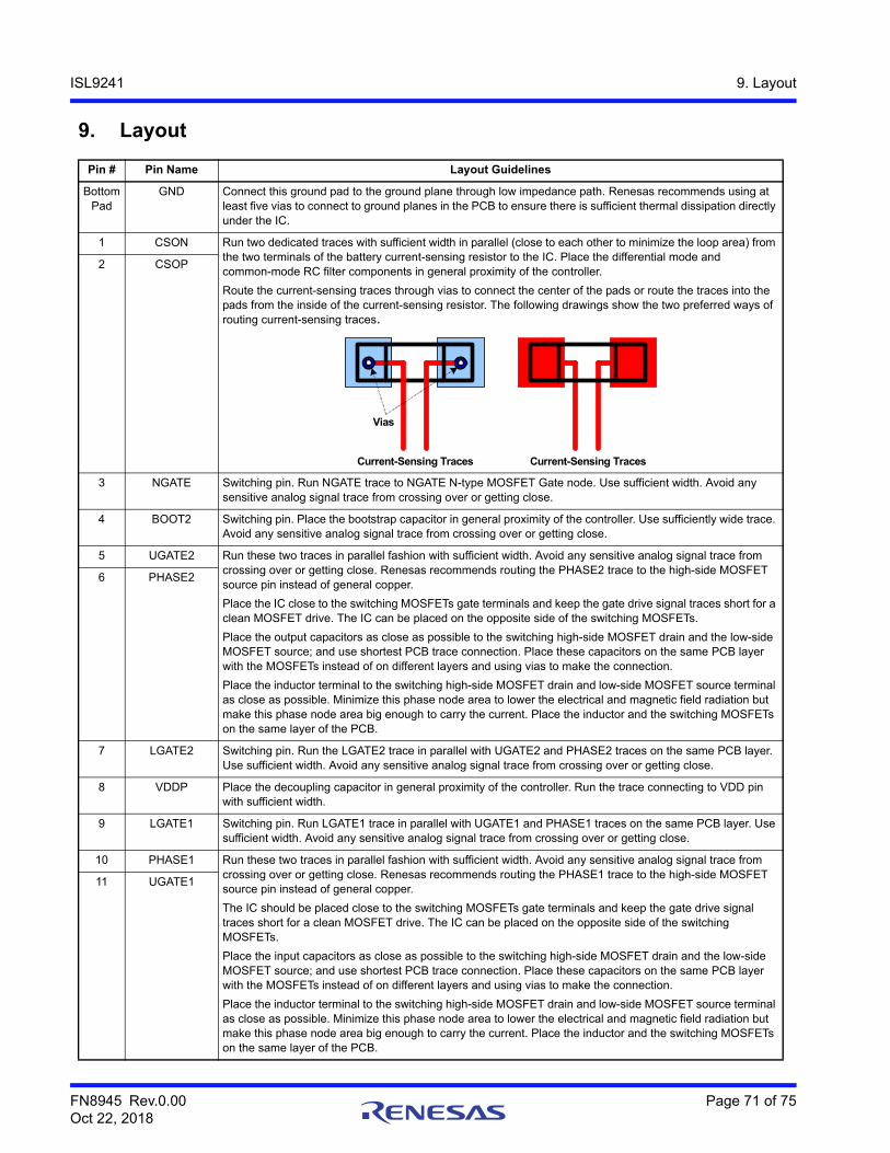
FN8945 Rev.0.00 Page 71 of 75Oct 22, 2018
ISL9241 9. Layout
9. Layout
Pin # Pin Name Layout Guidelines
BottomPad
GND Connect this ground pad to the ground plane through low impedance path. Renesas recommends using at least five vias to connect to ground planes in the PCB to ensure there is sufficient thermal dissipation directly under the IC.
1 CSON Run two dedicated traces with sufficient width in parallel (close to each other to minimize the loop area) from the two terminals of the battery current-sensing resistor to the IC. Place the differential mode and common-mode RC filter components in general proximity of the controller.
Route the current-sensing traces through vias to connect the center of the pads or route the traces into the pads from the inside of the current-sensing resistor. The following drawings show the two preferred ways of routing current-sensing traces.
2 CSOP
3 NGATE Switching pin. Run NGATE trace to NGATE N-type MOSFET Gate node. Use sufficient width. Avoid any sensitive analog signal trace from crossing over or getting close.
4 BOOT2 Switching pin. Place the bootstrap capacitor in general proximity of the controller. Use sufficiently wide trace. Avoid any sensitive analog signal trace from crossing over or getting close.
5 UGATE2 Run these two traces in parallel fashion with sufficient width. Avoid any sensitive analog signal trace from crossing over or getting close. Renesas recommends routing the PHASE2 trace to the high-side MOSFET source pin instead of general copper.
Place the IC close to the switching MOSFETs gate terminals and keep the gate drive signal traces short for a clean MOSFET drive. The IC can be placed on the opposite side of the switching MOSFETs.
Place the output capacitors as close as possible to the switching high-side MOSFET drain and the low-side MOSFET source; and use shortest PCB trace connection. Place these capacitors on the same PCB layer with the MOSFETs instead of on different layers and using vias to make the connection.
Place the inductor terminal to the switching high-side MOSFET drain and low-side MOSFET source terminal as close as possible. Minimize this phase node area to lower the electrical and magnetic field radiation but make this phase node area big enough to carry the current. Place the inductor and the switching MOSFETs on the same layer of the PCB.
6 PHASE2
7 LGATE2 Switching pin. Run the LGATE2 trace in parallel with UGATE2 and PHASE2 traces on the same PCB layer. Use sufficient width. Avoid any sensitive analog signal trace from crossing over or getting close.
8 VDDP Place the decoupling capacitor in general proximity of the controller. Run the trace connecting to VDD pin with sufficient width.
9 LGATE1 Switching pin. Run LGATE1 trace in parallel with UGATE1 and PHASE1 traces on the same PCB layer. Use sufficient width. Avoid any sensitive analog signal trace from crossing over or getting close.
10 PHASE1 Run these two traces in parallel fashion with sufficient width. Avoid any sensitive analog signal trace from crossing over or getting close. Renesas recommends routing the PHASE1 trace to the high-side MOSFET source pin instead of general copper.
The IC should be placed close to the switching MOSFETs gate terminals and keep the gate drive signal traces short for a clean MOSFET drive. The IC can be placed on the opposite side of the switching MOSFETs.
Place the input capacitors as close as possible to the switching high-side MOSFET drain and the low-side MOSFET source; and use shortest PCB trace connection. Place these capacitors on the same PCB layer with the MOSFETs instead of on different layers and using vias to make the connection.
Place the inductor terminal to the switching high-side MOSFET drain and low-side MOSFET source terminal as close as possible. Minimize this phase node area to lower the electrical and magnetic field radiation but make this phase node area big enough to carry the current. Place the inductor and the switching MOSFETs on the same layer of the PCB.
11 UGATE1
Current-Sensing Traces
Vias
Current-Sensing Traces
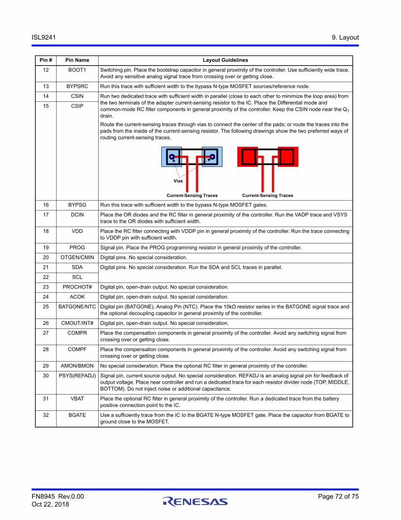
FN8945 Rev.0.00 Page 72 of 75Oct 22, 2018
ISL9241 9. Layout
12 BOOT1 Switching pin. Place the bootstrap capacitor in general proximity of the controller. Use sufficiently wide trace. Avoid any sensitive analog signal trace from crossing over or getting close.
13 BYPSRC Run this trace with sufficient width to the bypass N-type MOSFET sources/reference node.
14 CSIN Run two dedicated trace with sufficient width in parallel (close to each other to minimize the loop area) from the two terminals of the adapter current-sensing resistor to the IC. Place the Differential mode and common-mode RC filter components in general proximity of the controller. Keep the CSIN node near the Q1 drain.
Route the current-sensing traces through vias to connect the center of the pads; or route the traces into the pads from the inside of the current-sensing resistor. The following drawings show the two preferred ways of routing current-sensing traces.
15 CSIP
16 BYPSG Run this trace with sufficient width to the bypass N-type MOSFET gates.
17 DCIN Place the OR diodes and the RC filter in general proximity of the controller. Run the VADP trace and VSYS trace to the OR diodes with sufficient width.
18 VDD Place the RC filter connecting with VDDP pin in general proximity of the controller. Run the trace connecting to VDDP pin with sufficient width.
19 PROG Signal pin. Place the PROG programming resistor in general proximity of the controller.
20 OTGEN/CMIN Digital pins. No special consideration.
21 SDA Digital pins. No special consideration. Run the SDA and SCL traces in parallel.
22 SCL
23 PROCHOT# Digital pin, open-drain output. No special consideration.
24 ACOK Digital pin, open-drain output. No special consideration.
25 BATGONE/NTC Digital pin (BATGONE), Analog Pin (NTC). Place the 10kΩ resistor series in the BATGONE signal trace and the optional decoupling capacitor in general proximity of the controller.
26 CMOUT/INT# Digital pin, open-drain output. No special consideration.
27 COMPR Place the compensation components in general proximity of the controller. Avoid any switching signal from crossing over or getting close.
28 COMPF Place the compensation components in general proximity of the controller. Avoid any switching signal from crossing over or getting close.
29 AMON/BMON No special consideration. Place the optional RC filter in general proximity of the controller.
30 PSYS(REFADJ) Signal pin, current source output. No special consideration. REFADJ is an analog signal pin for feedback of output voltage. Place near controller and run a dedicated trace for each resistor divider node (TOP, MIDDLE, BOTTOM). Do not inject noise or additional capacitance.
31 VBAT Place the optional RC filter in general proximity of the controller. Run a dedicated trace from the battery positive connection point to the IC.
32 BGATE Use a sufficiently trace from the IC to the BGATE N-type MOSFET gate. Place the capacitor from BGATE to ground close to the MOSFET.
Pin # Pin Name Layout Guidelines
Current-Sensing Traces
Vias
Current-Sensing Traces
FN8945 Rev.0.00 Page 73 of 75Oct 22, 2018
ISL9241 10. Revision History
10. Revision History
Rev. Date Description
0.00 Oct 22, 2018 Initial release
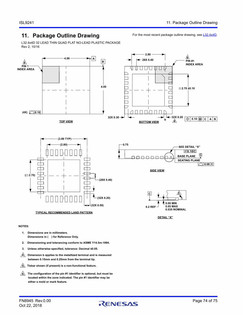
FN8945 Rev.0.00 Page 74 of 75Oct 22, 2018
ISL9241 11. Package Outline Drawing
11. Package Outline DrawingL32.4x4D 32 LEAD THIN QUAD FLAT NO-LEAD PLASTIC PACKAGE Rev 2, 10/16
PIN #16
INDEX AREA
TYPICAL RECOMMENDED LAND PATTERN
TOP VIEW
located within the zone indicated. The pin #1 identifier may be
Unless otherwise specified, tolerance: Decimal ±0.05.
Tiebar shown (if present) is a non-functional feature.
The configuration of the pin #1 identifier is optional, but must be
between 0.15mm and 0.25mm from the terminal tip.
Dimension b applies to the metallized terminal and is measured
Dimensions in ( ) for Reference Only.
Dimensioning and tolerancing conform to ASME Y14.5m-1994.
6.
either a mold or mark feature.
3.
5.
4.
2.
Dimensions are in millimeters.1.
NOTES:
DETAIL “X”
0.00 MIN0.05 MAX
5
0.2 REF
C
BOTTOM VIEW
INDEX AREAPIN 1
6
(4X) 0.10
4.00 AB
4.00
B0.10 M AC
28X 0.40
2.80
2.70 ±0.10
32X 0.20
432X 0.30
b
(32X 0.50)
(28X 0.40)
(32X 0.20)
(2.80)
(3.90 TYP)
( 2.70)
SEE DETAIL “X”
0.08 CSEATING PLANE
0.75
BASE PLANE CC0.10//
SIDE VIEW
0.035 NOMINAL
For the most recent package outline drawing, see L32.4x4D.
http://www.renesas.comRefer to "http://www.renesas.com/" for the latest and detailed information.
Renesas Electronics CorporationTOYOSU FORESIA, 3-2-24 Toyosu, Koto-ku, Tokyo 135-0061, JapanRenesas Electronics America Inc.1001 Murphy Ranch Road, Milpitas, CA 95035, U.S.A.Tel: +1-408-432-8888, Fax: +1-408-434-5351Renesas Electronics Canada Limited9251 Yonge Street, Suite 8309 Richmond Hill, Ontario Canada L4C 9T3Tel: +1-905-237-2004Renesas Electronics Europe LimitedDukes Meadow, Millboard Road, Bourne End, Buckinghamshire, SL8 5FH, U.KTel: +44-1628-651-700Renesas Electronics Europe GmbH
Arcadiastrasse 10, 40472 Düsseldorf, Germany Tel: +49-211-6503-0, Fax: +49-211-6503-1327Renesas Electronics (China) Co., Ltd.Room 1709 Quantum Plaza, No.27 ZhichunLu, Haidian District, Beijing, 100191 P. R. ChinaTel: +86-10-8235-1155, Fax: +86-10-8235-7679Renesas Electronics (Shanghai) Co., Ltd.Unit 301, Tower A, Central Towers, 555 Langao Road, Putuo District, Shanghai, 200333 P. R. China Tel: +86-21-2226-0888, Fax: +86-21-2226-0999Renesas Electronics Hong Kong LimitedUnit 1601-1611, 16/F., Tower 2, Grand Century Place, 193 Prince Edward Road West, Mongkok, Kowloon, Hong KongTel: +852-2265-6688, Fax: +852 2886-9022Renesas Electronics Taiwan Co., Ltd.13F, No. 363, Fu Shing North Road, Taipei 10543, TaiwanTel: +886-2-8175-9600, Fax: +886 2-8175-9670Renesas Electronics Singapore Pte. Ltd.80 Bendemeer Road, Unit #06-02 Hyflux Innovation Centre, Singapore 339949Tel: +65-6213-0200, Fax: +65-6213-0300Renesas Electronics Malaysia Sdn.Bhd.Unit 1207, Block B, Menara Amcorp, Amcorp Trade Centre, No. 18, Jln Persiaran Barat, 46050 Petaling Jaya, Selangor Darul Ehsan, MalaysiaTel: +60-3-7955-9390, Fax: +60-3-7955-9510Renesas Electronics India Pvt. Ltd.No.777C, 100 Feet Road, HAL 2nd Stage, Indiranagar, Bangalore 560 038, IndiaTel: +91-80-67208700, Fax: +91-80-67208777Renesas Electronics Korea Co., Ltd.17F, KAMCO Yangjae Tower, 262, Gangnam-daero, Gangnam-gu, Seoul, 06265 KoreaTel: +82-2-558-3737, Fax: +82-2-558-5338
SALES OFFICES
© 2018 Renesas Electronics Corporation. All rights reserved.Colophon 7.2
(Rev.4.0-1 November 2017)
Notice1. Descriptions of circuits, software and other related information in this document are provided only to illustrate the operation of semiconductor products and application examples. You are fully responsible for
the incorporation or any other use of the circuits, software, and information in the design of your product or system. Renesas Electronics disclaims any and all liability for any losses and damages incurred by
you or third parties arising from the use of these circuits, software, or information.
2. Renesas Electronics hereby expressly disclaims any warranties against and liability for infringement or any other claims involving patents, copyrights, or other intellectual property rights of third parties, by or
arising from the use of Renesas Electronics products or technical information described in this document, including but not limited to, the product data, drawings, charts, programs, algorithms, and application
examples.
3. No license, express, implied or otherwise, is granted hereby under any patents, copyrights or other intellectual property rights of Renesas Electronics or others.
4. You shall not alter, modify, copy, or reverse engineer any Renesas Electronics product, whether in whole or in part. Renesas Electronics disclaims any and all liability for any losses or damages incurred by
you or third parties arising from such alteration, modification, copying or reverse engineering.
5. Renesas Electronics products are classified according to the following two quality grades: “Standard” and “High Quality”. The intended applications for each Renesas Electronics product depends on the
product’s quality grade, as indicated below.
"Standard": Computers; office equipment; communications equipment; test and measurement equipment; audio and visual equipment; home electronic appliances; machine tools; personal electronic
equipment; industrial robots; etc.
"High Quality": Transportation equipment (automobiles, trains, ships, etc.); traffic control (traffic lights); large-scale communication equipment; key financial terminal systems; safety control equipment; etc.
Unless expressly designated as a high reliability product or a product for harsh environments in a Renesas Electronics data sheet or other Renesas Electronics document, Renesas Electronics products are
not intended or authorized for use in products or systems that may pose a direct threat to human life or bodily injury (artificial life support devices or systems; surgical implantations; etc.), or may cause
serious property damage (space system; undersea repeaters; nuclear power control systems; aircraft control systems; key plant systems; military equipment; etc.). Renesas Electronics disclaims any and all
liability for any damages or losses incurred by you or any third parties arising from the use of any Renesas Electronics product that is inconsistent with any Renesas Electronics data sheet, user’s manual or
other Renesas Electronics document.
6. When using Renesas Electronics products, refer to the latest product information (data sheets, user’s manuals, application notes, “General Notes for Handling and Using Semiconductor Devices” in the
reliability handbook, etc.), and ensure that usage conditions are within the ranges specified by Renesas Electronics with respect to maximum ratings, operating power supply voltage range, heat dissipation
characteristics, installation, etc. Renesas Electronics disclaims any and all liability for any malfunctions, failure or accident arising out of the use of Renesas Electronics products outside of such specified
ranges.
7. Although Renesas Electronics endeavors to improve the quality and reliability of Renesas Electronics products, semiconductor products have specific characteristics, such as the occurrence of failure at a
certain rate and malfunctions under certain use conditions. Unless designated as a high reliability product or a product for harsh environments in a Renesas Electronics data sheet or other Renesas
Electronics document, Renesas Electronics products are not subject to radiation resistance design. You are responsible for implementing safety measures to guard against the possibility of bodily injury, injury
or damage caused by fire, and/or danger to the public in the event of a failure or malfunction of Renesas Electronics products, such as safety design for hardware and software, including but not limited to
redundancy, fire control and malfunction prevention, appropriate treatment for aging degradation or any other appropriate measures. Because the evaluation of microcomputer software alone is very difficult
and impractical, you are responsible for evaluating the safety of the final products or systems manufactured by you.
8. Please contact a Renesas Electronics sales office for details as to environmental matters such as the environmental compatibility of each Renesas Electronics product. You are responsible for carefully and
sufficiently investigating applicable laws and regulations that regulate the inclusion or use of controlled substances, including without limitation, the EU RoHS Directive, and using Renesas Electronics
products in compliance with all these applicable laws and regulations. Renesas Electronics disclaims any and all liability for damages or losses occurring as a result of your noncompliance with applicable
laws and regulations.
9. Renesas Electronics products and technologies shall not be used for or incorporated into any products or systems whose manufacture, use, or sale is prohibited under any applicable domestic or foreign laws
or regulations. You shall comply with any applicable export control laws and regulations promulgated and administered by the governments of any countries asserting jurisdiction over the parties or
transactions.
10. It is the responsibility of the buyer or distributor of Renesas Electronics products, or any other party who distributes, disposes of, or otherwise sells or transfers the product to a third party, to notify such third
party in advance of the contents and conditions set forth in this document.
11. This document shall not be reprinted, reproduced or duplicated in any form, in whole or in part, without prior written consent of Renesas Electronics.
12. Please contact a Renesas Electronics sales office if you have any questions regarding the information contained in this document or Renesas Electronics products.
(Note 1) “Renesas Electronics” as used in this document means Renesas Electronics Corporation and also includes its directly or indirectly controlled subsidiaries.
(Note 2) “Renesas Electronics product(s)” means any product developed or manufactured by or for Renesas Electronics.
All trademarks and registered trademarks are the property of their respective owners.