Embed Size (px)
Citation preview
Integrated Silicon Solution, Inc. — www.issi.com 1Rev. A06/13/2012
Copyright©2012IntegratedSiliconSolution,Inc.Allrightsreserved.ISSIreservestherighttomakechangestothisspecificationanditsproductsatanytimewithoutnotice.ISSIassumesnoliabilityarisingoutoftheapplicationoruseofanyinformation,productsorservicesdescribedherein.Customersareadvisedtoobtainthelatestversionofthisdevicespecificationbeforerelyingonanypublishedinformationandbeforeplacingordersforproducts.
IS42/45S16100F, IS42VS16100F
IntegratedSiliconSolution,Inc.doesnotrecommendtheuseofanyofitsproductsinlifesupportapplicationswherethefailureormalfunctionoftheproductcanreason-ablybeexpectedtocausefailureofthelifesupportsystemortosignificantlyaffectitssafetyoreffectiveness.ProductsarenotauthorizedforuseinsuchapplicationsunlessIntegratedSiliconSolution,Inc.receiveswrittenassurancetoitssatisfaction,that:a.)theriskofinjuryordamagehasbeenminimized;b.)theuserassumeallsuchrisks;andc.)potentialliabilityofIntegratedSiliconSolution,Incisadequatelyprotectedunderthecircumstances
JUNE 2012
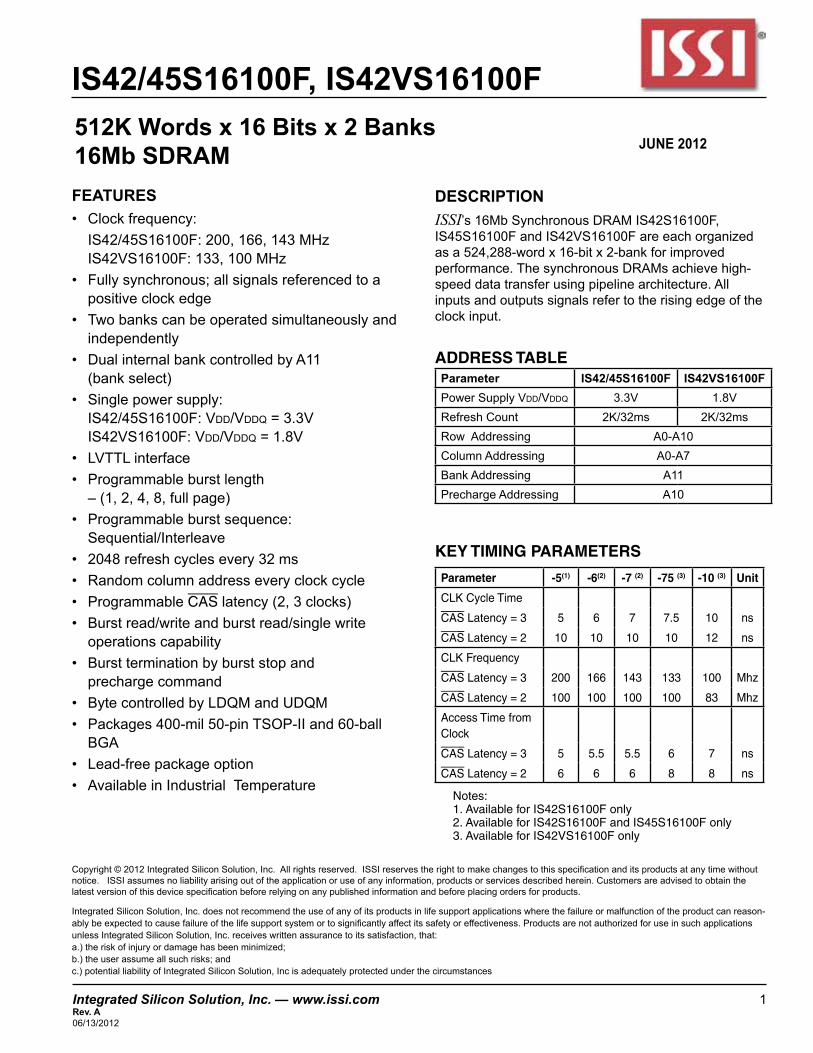
FEATURES• Clockfrequency: IS42/45S16100F:200,166,143MHzIS42VS16100F:133,100MHz
• Fullysynchronous;allsignalsreferencedtoapositiveclockedge
• Twobankscanbeoperatedsimultaneouslyandindependently
• DualinternalbankcontrolledbyA11(bankselect)
• Singlepowersupply:IS42/45S16100F:Vdd/Vddq=3.3VIS42VS16100F:Vdd/Vddq=1.8V
• LVTTLinterface• Programmableburstlength–(1,2,4,8,fullpage)
• Programmableburstsequence:Sequential/Interleave
• 2048refreshcyclesevery32ms• Randomcolumnaddresseveryclockcycle• ProgrammableCASlatency(2,3clocks)• Burstread/writeandburstread/singlewriteoperationscapability
• Burstterminationbyburststopandprechargecommand
• BytecontrolledbyLDQMandUDQM• Packages400-mil50-pinTSOP-IIand60-ballBGA
• Lead-freepackageoption• AvailableinIndustrialTemperature
DESCRIPTIONISSI’s16MbSynchronousDRAMIS42S16100F,IS45S16100FandIS42VS16100Fareeachorganizedasa524,288-wordx16-bitx2-bankforimprovedperformance.ThesynchronousDRAMsachievehigh-speeddatatransferusingpipelinearchitecture.Allinputsandoutputssignalsrefertotherisingedgeoftheclockinput.
512K Words x 16 Bits x 2 Banks16Mb SDRAM
Parameter IS42/45S16100F IS42VS16100FPowerSupplyVdd/Vddq 3.3V 1.8VRefreshCount 2K/32ms 2K/32msRowAddressing A0-A10ColumnAddressing A0-A7BankAddressing A11PrechargeAddressing A10
ADDRESS TABLE
Parameter -5(1) -6(2) -7 (2) -75 (3) -10 (3) Unit
CLK Cycle Time
CAS Latency = 3 5 6 7 7.5 10 ns
CAS Latency = 2 10 10 10 10 12 ns
CLK Frequency
CAS Latency = 3 200 166 143 133 100 Mhz
CAS Latency = 2 100 100 100 100 83 Mhz
Access Time from Clock
CAS Latency = 3 5 5.5 5.5 6 7 ns
CAS Latency = 2 6 6 6 8 8 ns
KEY TIMING PARAMETERS
Notes:1. Available for IS42S16100F only2. Available for IS42S16100F and IS45S16100F only3. Available for IS42VS16100F only
IS42/45S16100F, IS42VS16100F
2 Integrated Silicon Solution, Inc. — www.issi.com Rev. A
06/13/2012
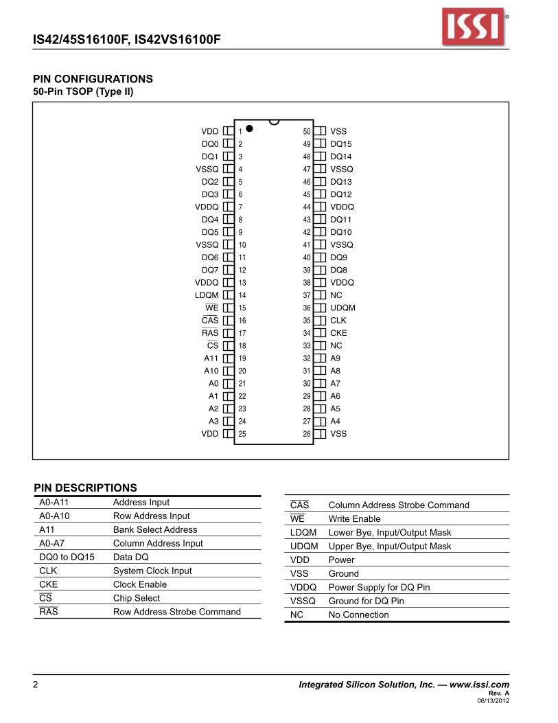
PIN DESCRIPTIONSA0-A11 AddressInputA0-A10 RowAddressInputA11 BankSelectAddressA0-A7 ColumnAddressInputDQ0toDQ15 DataDQCLK SystemClockInputCKE ClockEnableCS ChipSelectRAS RowAddressStrobeCommand
CAS ColumnAddressStrobeCommandWE WriteEnableLDQM LowerBye,Input/OutputMaskUDQM UpperBye,Input/OutputMaskVDD PowerVSS GroundVDDQ PowerSupplyforDQPinVSSQ GroundforDQPinNC NoConnection
PIN CONFIGURATIONS50-Pin TSOP (Type II)
1
2
3
4
5
6
7
8
9
10
11
12
13
14
15
16
17
18
19
20
21
22
23
24
25
50
49
48
47
46
45
44
43
42
41
40
39
38
37
36
35
34
33
32
31
30
29
28
27
26
VDD
DQ0
DQ1
VSSQ
DQ2
DQ3
VDDQ
DQ4
DQ5
VSSQ
DQ6
DQ7
VDDQ
LDQM
WE
CAS
RAS
CS
A11
A10
A0
A1
A2
A3
VDD
VSS
DQ15
DQ14
VSSQ
DQ13
DQ12
VDDQ
DQ11
DQ10
VSSQ
DQ9
DQ8
VDDQ
NC
UDQM
CLK
CKE
NC
A9
A8
A7
A6
A5
A4
VSS
Integrated Silicon Solution, Inc. — www.issi.com 3Rev. A06/13/2012
IS42/45S16100F, IS42VS16100F
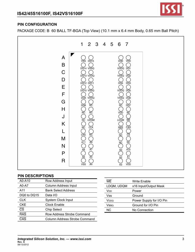
PIN CONFIGURATIONPACKAGECODE:B60BALLTF-BGA(TopView)(10.1mmx6.4mmBody,0.65mmBallPitch)
1 2 3 4 5 6 7
A
B
C
D
E
F
G
H
J
K
L
M
N
P
R
VSS
DQ14
DQ13
DQ12
DQ10
DQ9
DQ8
NC
NC
NC
CKE
A11
A8
A6
VSS
DQ15
VSSQ
VDDQ
DQ11
VSSQ
VDDQ
NC
NC
UDQM
CLK
NC
A9
A7
A5
A4
DQ0
VDDQ
VSSQ
DQ4
VDDQ
VSSQ
NC
VDD
LDQM
RAS
NC
NC
A0
A2
A3
VDD
DQ1
DQ2
DQ3
DQ5
DQ6
DQ7
NC
WE
CAS
CS
NC
A10
A1
VDD
PIN DESCRIPTIONSA0-A10 RowAddressInputA0-A7 ColumnAddressInputA11 BankSelectAddressDQ0toDQ15 DataI/OCLK SystemClockInputCKE ClockEnableCS ChipSelectRAS RowAddressStrobeCommandCAS ColumnAddressStrobeCommand
WE WriteEnableLDQM,UDQM x16Input/OutputMaskVdd PowerVss GroundVddq PowerSupplyforI/OPinVssq GroundforI/OPinNC NoConnection
IS42/45S16100F, IS42VS16100F
4 Integrated Silicon Solution, Inc. — www.issi.com Rev. A
06/13/2012
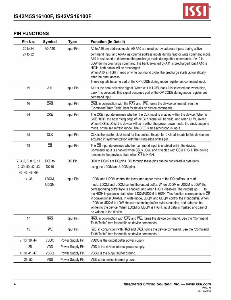
PIN FUNCTIONS
Pin No. Symbol Type Function (In Detail)
20to24 A0-A10 InputPin A0toA10areaddressinputs.A0-A10areusedasrowaddressinputsduringactive 27to32 commandinputandA0-A7ascolumnaddressinputsduringreadorwritecommandinput.
A10isalsousedtodeterminetheprechargemodeduringothercommands.IfA10isLOWduringprechargecommand,thebankselectedbyA11isprecharged,butifA10isHIGH,bothbankswillbeprecharged.WhenA10isHIGHinreadorwritecommandcycle,theprechargestartsautomaticallyaftertheburstaccess.ThesesignalsbecomepartoftheOPCODEduringmoderegistersetcommandinput.
19 A11 InputPin A11isthebankselectionsignal.WhenA11isLOW,bank0isselectedandwhenhigh,bank1isselected.ThissignalbecomespartoftheOPCODEduringmoderegistersetcommandinput.
16 CAS InputPin CAS,inconjunctionwiththeRASandWE,formsthedevicecommand.Seethe“CommandTruthTable”itemfordetailsondevicecommands.
34 CKE InputPin TheCKEinputdetermineswhethertheCLKinputisenabledwithinthedevice.WhenisCKEHIGH,thenextrisingedgeoftheCLKsignalwillbevalid,andwhenLOW,invalid.WhenCKEisLOW,thedevicewillbeineitherthepower-downmode,theclocksuspendmode,ortheselfrefreshmode.TheCKEisanasynchronousinput.
35 CLK InputPin CLKisthemasterclockinputforthisdevice.ExceptforCKE,allinputstothisdeviceareacquiredinsynchronizationwiththerisingedgeofthispin.
18 CS InputPin TheCSinputdetermineswhethercommandinputisenabledwithinthedevice. CommandinputisenabledwhenCSisLOW,anddisabledwithCSisHIGH.ThedeviceremainsinthepreviousstatewhenCSisHIGH.
2,3,5,6,8,9,11 DQ0to DQPin DQ0toDQ15areDQpins.DQthroughthesepinscanbecontrolledinbyteunits 12,39,40,42,43, DQ15 usingtheLDQMandUDQMpins. 45,46,48,49
14,36 LDQM, InputPin LDQMandUDQMcontrolthelowerandupperbytesoftheDQbuffers.Inread UDQM mode,LDQMandUDQMcontroltheoutputbuffer.WhenLDQMorUDQMisLOW,the
correspondingbufferbyteisenabled,andwhenHIGH,disabled.Theoutputsgo totheHIGHimpedancestatewhenLDQM/UDQMisHIGH.ThisfunctioncorrespondstoOEinconventionalDRAMs.Inwritemode,LDQMandUDQMcontroltheinputbuffer.WhenLDQMorUDQMisLOW,thecorrespondingbufferbyteisenabled,anddatacanbewrittentothedevice.WhenLDQMorUDQMisHIGH,inputdataismaskedandcannotbewrittentothedevice.
17 RAS InputPin RAS,inconjunctionwithCASandWE,formsthedevicecommand.Seethe“CommandTruthTable”itemfordetailsondevicecommands.
15 WE InputPin WE,inconjunctionwithRASandCAS,formsthedevicecommand.Seethe“CommandTruthTable”itemfordetailsondevicecommands.
7,13,38,44 VddQ PowerSupplyPin VddQistheoutputbufferpowersupply.
1,25 Vdd PowerSupplyPin Vddisthedeviceinternalpowersupply.
4,10,41,47 VSSQ PowerSupplyPin VSSQistheoutputbufferground.
26,50 VSS PowerSupplyPin VSSisthedeviceinternalground.
Integrated Silicon Solution, Inc. — www.issi.com 5Rev. A06/13/2012
IS42/45S16100F, IS42VS16100F
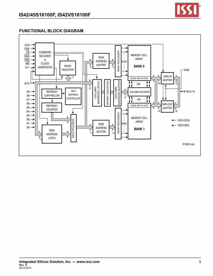
FUNCTIONAL BLOCK DIAGRAM
CLKCKE
CSRASCASWEA11
A9A8A7A6A5A4A3A2A1A0
A10
COMMANDDECODER
&CLOCK
GENERATOR MODEREGISTER
REFRESHCONTROLLER
REFRESHCOUNTER
SELF
REFRESH
CONTROLLER
ROWADDRESS
LATCH MU
LTIP
LE
XE
R
ROWADDRESSBUFFER
ROWADDRESSBUFFER
CO
LU
MN
AD
DR
ES
S L
AT
CH
BU
RS
T C
OU
NT
ER
CO
LU
MN
AD
DR
ES
S B
UF
FE
RR
OW
DE
CO
DE
RR
OW
DE
CO
DE
R
MEMORY CELLARRAY
BANK 0
COLUMN DECODER
MEMORY CELLARRAY
BANK 1
DATA INBUFFER
DATA OUTBUFFER
SENSE AMP I/O GATE
SENSE AMP I/O GATE
2048
2048
DQM
DQ 0-15
VDD/VDDQ
VSS/VSSQ
11
11
11 11
8
11 11
8
16
16 16
16 256
256
S16BLK.eps
IS42/45S16100F, IS42VS16100F
6 Integrated Silicon Solution, Inc. — www.issi.com Rev. A
06/13/2012
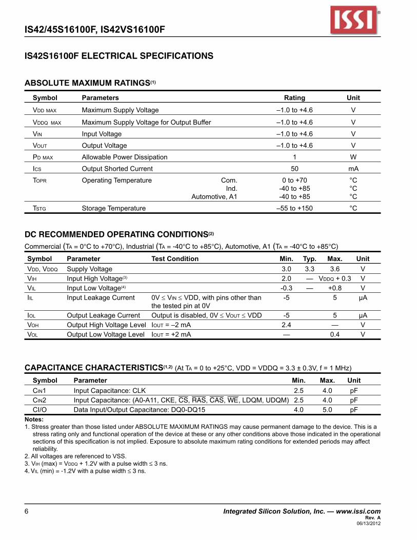
ABSOLUTE MAXIMUM RATINGS(1)
Symbol Parameters Rating Unit
Vdd max MaximumSupplyVoltage –1.0to+4.6 V
Vddqmax MaximumSupplyVoltageforOutputBuffer –1.0to+4.6 V
Vin InputVoltage –1.0to+4.6 V
Vout OutputVoltage –1.0to+4.6 V
Pd max AllowablePowerDissipation 1 W
Ics outputShortedCurrent 50 mA
Topr operatingTemperature Com. 0to+70 °C Ind. -40to+85 °C Automotive,A1 -40to+85 °C
Tstg StorageTemperature –55to+150 °C
DC RECOMMENDED OPERATING CONDITIONS(2) Commercial (Ta = 0°C to +70°C), Industrial (Ta = -40°C to +85°C), Automotive, A1 (Ta = -40°C to +85°C)
Symbol Parameter Test Condition Min. Typ. Max. UnitVdd, Vddq SupplyVoltage 3.0 3.3 3.6 VVih InputHighVoltage(3) 2.0 — Vddq +0.3 VVil InputLowVoltage(4) -0.3 — +0.8 Viil InputLeakageCurrent 0V≤Vin≤Vdd,withpinsotherthan -5 5 µA thetestedpinat0Viol OutputLeakageCurrent Outputisdisabled,0V≤Vout≤Vdd -5 5 µAVoh OutputHighVoltageLevel iout=–2mA 2.4 — VVol OutputLowVoltageLevel iout=+2mA — 0.4 V
CAPACITANCE CHARACTERISTICS(1,2) (AtTa=0to+25°C,VDD=VDDQ=3.3±0.3V,f=1MHz)
Symbol Parameter Min. Max. Unit Cin1 InputCapacitance:CLK 2.5 4.0 pF Cin2 InputCapacitance:(A0-A11,CKE, CS, RAS,CAS,WE,LDQM,UDQM) 2.5 4.0 pF CI/O DataInput/OutputCapacitance:DQ0-DQ15 4.0 5.0 pFNotes:1.StressgreaterthanthoselistedunderABSOLUTEMAXIMUMRATINGSmaycausepermanentdamagetothedevice.Thisisa
stressratingonlyandfunctionaloperationofthedeviceattheseoranyotherconditionsabovethoseindicatedintheoperationalsectionsofthisspecificationisnotimplied.Exposuretoabsolutemaximumratingconditionsforextendedperiodsmayaffectreliability.
2.AllvoltagesarereferencedtoVSS.3.Vih(max)=Vddq+1.2Vwithapulsewidth≤3ns.4. Vil (min) = -1.2V with a pulse width ≤ 3 ns.
IS42S16100F ELECTRICAL SPECIFICATIONS
Integrated Silicon Solution, Inc. — www.issi.com 7Rev. A06/13/2012
IS42/45S16100F, IS42VS16100F
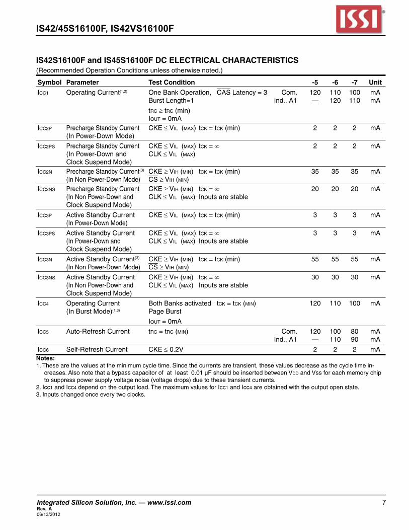
IS42S16100F and IS45S16100F DC ELECTRICAL CHARACTERISTICS
(Recommended Operation Conditions unless otherwise noted.)
Symbol Parameter Test Condition -5 -6 -7 Unit
icc1 Operating Current(1,2) One Bank Operation, CAS Latency = 3 Com. 120 110 100 mA Burst Length=1 Ind., A1 — 120 110 mA
trc ≥ trc (min) Iout = 0mA icc2p Precharge Standby Current CKE ≤ Vil (max) tck = tck (min) 2 2 2 mA (In Power-Down Mode)
Icc2ps Precharge Standby Current CKE ≤ Vil (max) tck=∞ 2 2 2 mA (In Power-Down and CLK ≤ Vil (max) Clock Suspend Mode)icc2n Precharge Standby Current(3) CKE ≥ Vih (min) tck = tck (min) 35 35 35 mA (In Non Power-Down Mode) CS ≥ Vih (min) Icc2ns Precharge Standby Current CKE ≥ Vih (min) tck=∞ 20 20 20 mA (In Non Power-Down and CLK ≤ Vil (max) Inputs are stable Clock Suspend Mode)
icc3P Active Standby Current CKE ≤ Vil (max) tck = tck (min) 3 3 3 mA (In Power-Down Mode)
Icc3Ps Active Standby Current CKE ≤ Vil (max) tck=∞ 3 3 3 mA (In Power-Down and CLK ≤ Vil (max) Inputs are stable Clock Suspend Mode)
icc3n Active Standby Current(3) CKE ≥ Vih (min) tck = tck (min) 55 55 55 mA (In Non Power-Down Mode) CS ≥ Vih (min)
Icc3ns Active Standby Current CKE ≥ Vih (min) tck=∞ 30 30 30 mA (In Non Power-Down and CLK ≤ Vil (max) Inputs are stable Clock Suspend Mode)
icc4 Operating Current Both Banks activated tck = tck (min) 120 110 100 mA (In Burst Mode)(1,3) Page Burst
Iout= 0mA
icc5 Auto-Refresh Current trc = trc(min) Com. 120 100 80 mA Ind., A1 — 110 90 mA
icc6 Self-Refresh Current CKE ≤ 0.2V 2 2 2 mANotes:1. These are the values at the minimum cycle time. Since the currents are transient, these values decrease as the cycle time in-
creases. Also note that a bypass capacitor of at least 0.01 µF should be inserted between Vddand Vss for each memory chip to suppress power supply voltage noise (voltage drops) due to these transient currents.
2. Icc1 and Icc4 depend on the output load. The maximum values for Icc1 and Icc4 are obtained with the output open state.3. Inputs changed once every two clocks.
IS42/45S16100F, IS42VS16100F
8 Integrated Silicon Solution, Inc. — www.issi.com Rev. A
06/13/2012
IS42S16100F and IS45S16100F AC CHARACTERISTICS(1,2,3)
-5 -6 -7 Symbol Parameter Min. Max. Min. Max. Min. Max. Units
tck3 ClockCycleTime CASLatency=3 5 — 6 — 7 — ns tck2 CASLatency=2 10 — 10 — 10 — ns
tac3 AccessTimeFromCLK(4) CASLatency=3 — 5 — 5.5 — 5.5 ns tac2 CASLatency=2 — 6 — 6 — 6 ns
tchi CLKHIGHLevelWidth 2 — 2.5 — 2.5 — ns
tcl CLKLOWLevelWidth 2 — 2.5 — 2.5 — ns
toh3 OutputDataHoldTime CASLatency=3 2 — 2.0 — 2.0 — ns toh2 CAS Latency=2 2.5 — 2.5 — 2.5 — ns
tlz OutputLOWImpedanceTime 0 — 0 — 0 — ns
thz3 OutputHIGHImpedanceTime(5) CASLatency=3 — 5 — 5.5 — 5.5 ns thz2 CASLatency=2 — 6 — 6 — 6 ns
tds InputDataSetupTime 2 — 2 — 2 — ns
tdh InputDataHoldTime 1 — 1 — 1 — ns
tas AddressSetupTime 2 — 2 — 2 — ns
tah AddressHoldTime 1 — 1 — 1 — ns
tcks CKESetupTime 2 — 2 — 2 — ns
tckh CKEHoldTime 1 — 1 — 1 — ns
tcka CKEtoCLKRecoveryDelayTime 1CLK+3 — 1CLK+3 — 1CLK+3 — ns
tcs CommandSetupTime(CS,RAS,CAS,WE,DQM) 2 — 2 — 2 — ns
tch CommandHoldTime(CS,RAS,CAS,WE,DQM) 1 — 1 — 1 — ns
trc CommandPeriod(REFtoREF/ACTtoACT) 50 — 54 — 63 — ns
tras CommandPeriod(ACTtoPRE) 35 100,000 36 100,000 42 100,000 ns
trp CommandPeriod(PREtoACT) 15 — 18 — 20 — ns
trcd ActiveCommandToRead/WriteCommandDelayTime 15 — 18 — 20 — ns
trrd CommandPeriod(ACT[0]toACT[1]) 10 — 12 — 14 — ns
tdpl3 InputDataToPrecharge CASLatency=3 2CLK — 2CLK — 2CLK — ns tdpl2 CommandDelaytime CAS Latency=2 2CLK — 2CLK — 2CLK — ns
tdal3 InputDataToActive/Refresh CASLatency=3 2CLK+trp — 2CLK+trp — 2CLK+trp — ns tdal2 CommandDelaytime(DuringAuto-Precharge) CAS Latency=2 2CLK+trp — 2CLK+trp — 2CLK+trp — ns
txsr ExitSelf-RefreshtoActiveTime 55 — 60 — 70 — ns
tt TransitionTime 0.3 1.2 0.3 1.2 0.3 1.2 ns
tref RefreshCycleTime(2048) — 32 — 32 — 32 msNotes:1.Whenpowerisfirstapplied,memoryoperationshouldbestarted100µsafterVdd andVddq reachtheirstipulatedvoltages.Alsonotethatthepower-on sequencemustbeexecutedbeforestartingmemoryoperation.2.measuredwithtt =1ns.Ifclockrisingtimeislongerthan1ns,(tt/2-0.5)nsshouldbeaddedtotheparameter.3.Thereferencelevelis1.4Vwhenmeasuringinputsignaltiming.RiseandfalltimesaremeasuredbetweenVih (min.)andVil (max.).4.Accesstimeismeasuredat1.4Vwiththeloadshowninthefigurethatfollows.5.Thetimethz (max.)isdefinedasthetimerequiredfortheoutputvoltagetotransitionby±200mVfromVoh (min.)orVol(max.)whenthe outputisinthehighimpedancestate.
Integrated Silicon Solution, Inc. — www.issi.com 9Rev. A06/13/2012
IS42/45S16100F, IS42VS16100F
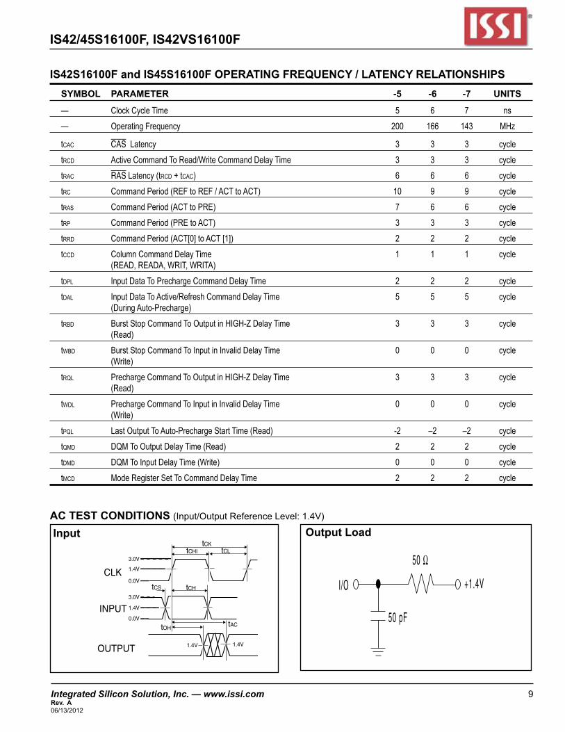
IS42S16100F and IS45S16100F OPERATING FREQUENCY / LATENCY RELATIONSHIPS SYMBOL PARAMETER -5 -6 -7 UNITS
— ClockCycleTime 5 6 7 ns
— OperatingFrequency 200 166 143 MHz
tcac CASLatency 3 3 3 cycle
trcd ActiveCommandToRead/WriteCommandDelayTime 3 3 3 cycle
trac RASLatency(trcd+tcac) 6 6 6 cycle
trc CommandPeriod(REFtoREF/ACTtoACT) 10 9 9 cycle
tras CommandPeriod(ACTtoPRE) 7 6 6 cycle
trp CommandPeriod(PREtoACT) 3 3 3 cycle
trrd CommandPeriod(ACT[0]toACT[1]) 2 2 2 cycle
tccd ColumnCommandDelayTime 1 1 1 cycle (READ,READA,WRIT,WRITA)
tdpl InputDataToPrechargeCommandDelayTime 2 2 2 cycle
tdal InputDataToActive/RefreshCommandDelayTime 5 5 5 cycle (DuringAuto-Precharge)
trbd BurstStopCommandToOutputinHIGH-ZDelayTime 3 3 3 cycle (Read)
twbd BurstStopCommandToInputinInvalidDelayTime 0 0 0 cycle (Write)
trql PrechargeCommandToOutputinHIGH-ZDelayTime 3 3 3 cycle (Read)
twdl PrechargeCommandToInputinInvalidDelayTime 0 0 0 cycle (Write)
tpql LastOutputToAuto-PrechargeStartTime(Read) -2 –2 –2 cycle
tqmd DQMToOutputDelayTime(Read) 2 2 2 cycle
tdmd DQMToInputDelayTime(Write) 0 0 0 cycle
tmcd ModeRegisterSetToCommandDelayTime 2 2 2 cycle
AC TEST CONDITIONS (Input/OutputReferenceLevel:1.4V)
I/O
50 Ω
+1.4V
50 pF
Output LoadInput
tOH tAC
1.4V 1.4V
tCHtCS
tCKtCHI tCL
3.0V
1.4V
0.0V
3.0V
1.4V
0.0V
CLK
INPUT
OUTPUT
IS42/45S16100F, IS42VS16100F
10 Integrated Silicon Solution, Inc. — www.issi.com Rev. A
06/13/2012
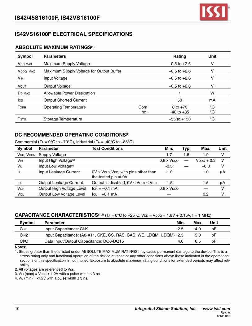
ABSOLUTE MAXIMUM RATINGS(1)
Symbol Parameters Rating Unit
Vddmax Maximum Supply Voltage –0.5 to +2.6 V
Vddq max Maximum Supply Voltage for Output Buffer –0.5 to +2.6 V
Vin Input Voltage –0.5 to +2.6 V
Vout Output Voltage –0.5 to +2.6 V
Pdmax Allowable Power Dissipation 1 W
Ics output Shorted Current 50 mA
Topr operating Temperature Com 0 to +70 °C Ind. -40 to +85 °C
Tstg Storage Temperature –55 to +150 °C
DC RECOMMENDED OPERATING CONDITIONS(2) Commercial (Ta = 0°C to +70°C), Industrial (Ta = -40°C to +85°C)
Symbol Parameter Test Conditions Min. Typ. Max. Unit
Vdd,Vddq Supply Voltage 1.7 1.8 1.9 V Vih Input High Voltage(3) 0.8 x Vddq — Vddq+ 0.3 V Vil Input Low Voltage(4) -0.3 — +0.3 V iil Input Leakage Current 0V ≤ Vin ≤ Vdd, with pins other than -1.0 1.0 mA the tested pin at 0V iol Output Leakage Current Output is disabled, 0V ≤ Vout ≤ Vdd -1.5 1.5 mA Voh Output High Voltage Level ioh = –0.1 mA 0.9 x Vddq — V Vol Output Low Voltage Level iol = +0.1 mA — 0.2 V
CAPACITANCE CHARACTERISTICS(1,2) (Ta = 0°C to +25°C, Vdd = Vddq=1.8V + 0.15V, f = 1 MHz)
Symbol Parameter Min. Max. Unit
Cin1 Input Capacitance: CLK 2.5 4.0 pF
Cin2 Input Capacitance: (A0-A11, CKE, CS, RAS, CAS, WE, LDQM, UDQM) 2.5 5.0 pF
CI/O Data Input/Output Capacitance: DQ0-DQ15 4.0 6.5 pFNotes:1. Stress greater than those listed under ABSOLUTE MAXIMUM RATINGS may cause permanent damage to the device. This is a
stress rating only and functional operation of the device at these or any other conditions above those indicated in the operational sections of this specification is not implied. Exposure to absolute maximum rating conditions for extended periods may affect reli-ability.
2. All voltages are referenced to Vss.3. Vih (max) = Vddq + 1.2V with a pulse width ≤ 3 ns.4. Vil (min) = -1.2V with a pulse width ≤ 3 ns.
IS42VS16100F ELECTRICAL SPECIFICATIONS
Integrated Silicon Solution, Inc. — www.issi.com 11Rev. A06/13/2012
IS42/45S16100F, IS42VS16100F
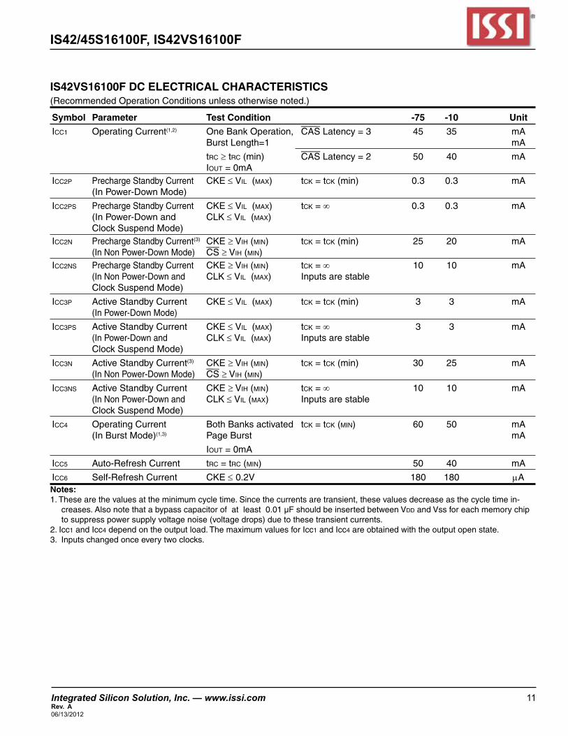
IS42VS16100F DC ELECTRICAL CHARACTERISTICS
(Recommended Operation Conditions unless otherwise noted.)
Symbol Parameter Test Condition -75 -10 Unit
icc1 Operating Current(1,2) One Bank Operation, CAS Latency = 3 45 35 mA Burst Length=1 mA
trc ≥ trc (min) CAS Latency = 2 50 40 mA Iout = 0mA icc2p Precharge Standby Current CKE ≤ Vil (max) tck = tck (min) 0.3 0.3 mA (In Power-Down Mode)
Icc2ps Precharge Standby Current CKE ≤ Vil (max) tck=∞ 0.3 0.3 mA (In Power-Down and CLK ≤ Vil (max) Clock Suspend Mode)icc2n Precharge Standby Current(3) CKE ≥ Vih (min) tck = tck (min) 25 20 mA (In Non Power-Down Mode) CS ≥ Vih (min) Icc2ns Precharge Standby Current CKE ≥ Vih (min) tck=∞ 10 10 mA (In Non Power-Down and CLK ≤ Vil (max) Inputs are stable Clock Suspend Mode)
icc3P Active Standby Current CKE ≤ Vil (max) tck = tck (min) 3 3 mA (In Power-Down Mode)
Icc3Ps Active Standby Current CKE ≤ Vil (max) tck=∞ 3 3 mA (In Power-Down and CLK ≤ Vil (max) Inputs are stable Clock Suspend Mode)
icc3n Active Standby Current(3) CKE ≥ Vih (min) tck = tck (min) 30 25 mA (In Non Power-Down Mode) CS ≥ Vih (min)
Icc3ns Active Standby Current CKE ≥ Vih (min) tck=∞ 10 10 mA (In Non Power-Down and CLK ≤ Vil (max) Inputs are stable Clock Suspend Mode)
icc4 Operating Current Both Banks activated tck = tck (min) 60 50 mA (In Burst Mode)(1,3) Page Burst mA
Iout= 0mA
icc5 Auto-Refresh Current trc = trc(min) 50 40 mA
icc6 Self-Refresh Current CKE ≤ 0.2V 180 180 µANotes:1. These are the values at the minimum cycle time. Since the currents are transient, these values decrease as the cycle time in-
creases. Also note that a bypass capacitor of at least 0.01 µF should be inserted between Vddand Vss for each memory chip to suppress power supply voltage noise (voltage drops) due to these transient currents.
2. Icc1 and Icc4 depend on the output load. The maximum values for Icc1 and Icc4 are obtained with the output open state.3. Inputs changed once every two clocks.
IS42/45S16100F, IS42VS16100F
12 Integrated Silicon Solution, Inc. — www.issi.com Rev. A
06/13/2012
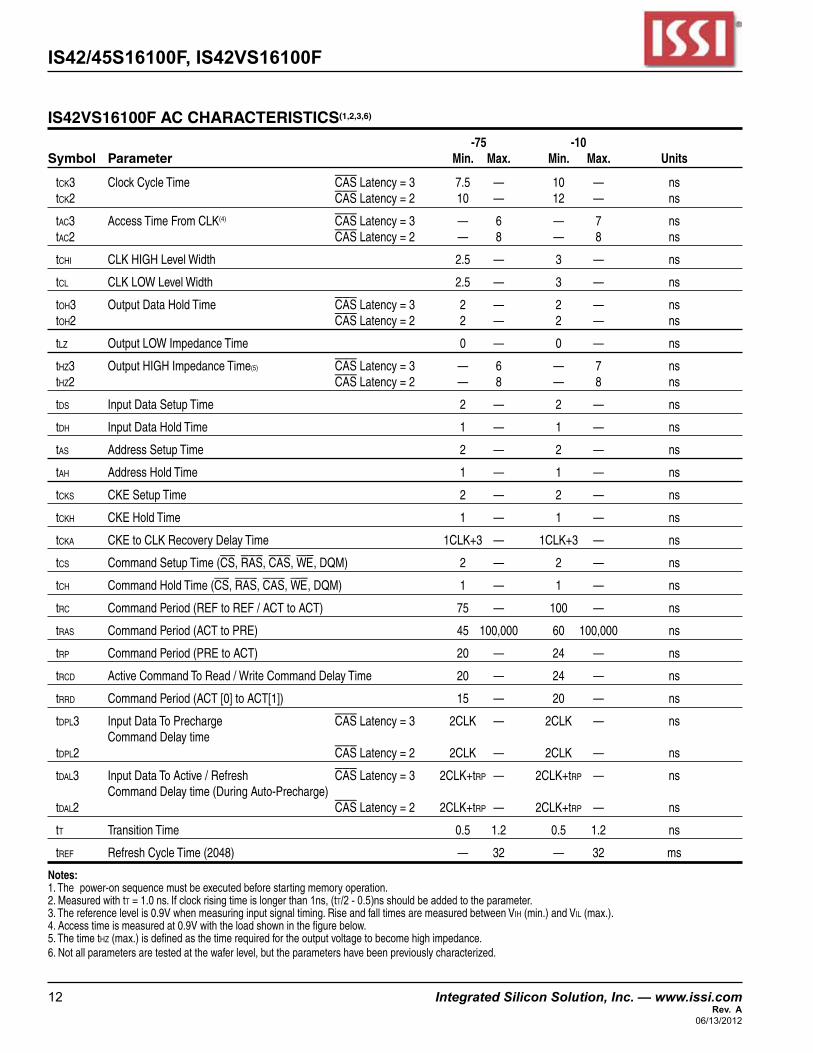
IS42VS16100F AC CHARACTERISTICS(1,2,3,6)
-75 -10 Symbol Parameter Min. Max. Min. Max. Units
tck3 Clock Cycle Time CAS Latency = 3 7.5 — 10 — ns tck2 CAS Latency = 2 10 — 12 — ns
tac3 Access Time From CLK(4) CAS Latency = 3 — 6 — 7 ns tac2 CAS Latency = 2 — 8 — 8 ns
tchi CLK HIGH Level Width 2.5 — 3 — ns
tcl CLK LOW Level Width 2.5 — 3 — ns
toh3 Output Data Hold Time CAS Latency = 3 2 — 2 — ns toh2 CAS Latency = 2 2 — 2 — ns
tlz Output LOW Impedance Time 0 — 0 — ns
thz3 Output HIGH Impedance Time(5) CAS Latency = 3 — 6 — 7 ns thz2 CAS Latency = 2 — 8 — 8 ns
tds Input Data Setup Time 2 — 2 — ns
tdh Input Data Hold Time 1 — 1 — ns
tas Address Setup Time 2 — 2 — ns
tah Address Hold Time 1 — 1 — ns
tcks CKE Setup Time 2 — 2 — ns
tckh CKE Hold Time 1 — 1 — ns
tcka CKE to CLK Recovery Delay Time 1CLK+3 — 1CLK+3 — ns
tcs Command Setup Time (CS, RAS, CAS, WE, DQM) 2 — 2 — ns
tch Command Hold Time (CS, RAS, CAS, WE, DQM) 1 — 1 — ns
trc Command Period (REF to REF / ACT to ACT) 75 — 100 — ns
tras Command Period (ACT to PRE) 45 100,000 60 100,000 ns
trp Command Period (PRE to ACT) 20 — 24 — ns
trcd Active Command To Read / Write Command Delay Time 20 — 24 — ns
trrd Command Period (ACT [0] to ACT[1]) 15 — 20 — ns
tdpl3 Input Data To Precharge CAS Latency = 3 2CLK — 2CLK — ns Command Delay time tdpl2 CAS Latency = 2 2CLK — 2CLK — ns
tdal3 Input Data To Active / Refresh CAS Latency = 3 2CLK+trp — 2CLK+trp — ns Command Delay time (During Auto-Precharge) tdal2 CAS Latency = 2 2CLK+trp — 2CLK+trp — ns
tt Transition Time 0.5 1.2 0.5 1.2 ns
tref Refresh Cycle Time (2048) — 32 — 32 ms
Notes:1. The power-on sequence must be executed before starting memory operation.2. measured with tt= 1.0 ns. Ifclockrisingtimeislongerthan1ns,(tt/2-0.5)nsshouldbeaddedtotheparameter.3. The reference level is 0.9V when measuring input signal timing. Rise and fall times are measured between Vih(min.) and Vil(max.).4. Access time is measured at 0.9V with the load shown in the figure below.5. The time thz(max.) is defined as the time required for the output voltage to become high impedance.6. Not all parameters are tested at the wafer level, but the parameters have been previously characterized.
Integrated Silicon Solution, Inc. — www.issi.com 13Rev. A06/13/2012
IS42/45S16100F, IS42VS16100F
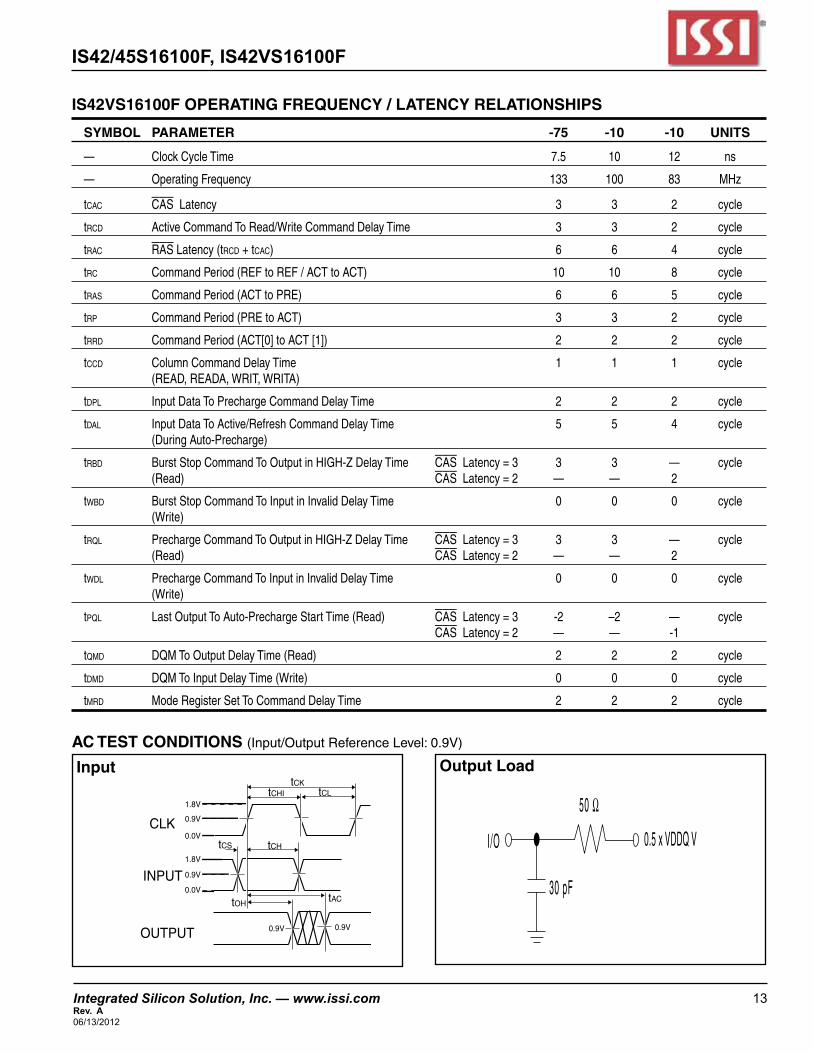
AC TEST CONDITIONS (Input/Output Reference Level: 0.9V)
I/O
50 Ω
0.5 x VDDQ V
30 pF
Output LoadInput
tOH tAC
0.9V 0.9V
tCHtCS
tCKtCHI tCL
1.8V
0.9V
0.0V
1.8V
0.9V
0.0V
CLK
INPUT
OUTPUT
IS42VS16100F OPERATING FREQUENCY / LATENCY RELATIONSHIPS
SYMBOL PARAMETER -75 -10 -10 UNITS
— Clock Cycle Time 7.5 10 12 ns
— Operating Frequency 133 100 83 MHz
tcac CAS Latency 3 3 2 cycle
trcd Active Command To Read/Write Command Delay Time 3 3 2 cycle
trac RAS Latency (trcd + tcac) 6 6 4 cycle
trc Command Period (REF to REF / ACT to ACT) 10 10 8 cycle
tras Command Period (ACT to PRE) 6 6 5 cycle
trp Command Period (PRE to ACT) 3 3 2 cycle
trrd Command Period (ACT[0] to ACT [1]) 2 2 2 cycle
tccd Column Command Delay Time 1 1 1 cycle (READ, READA, WRIT, WRITA)
tdpl Input Data To Precharge Command Delay Time 2 2 2 cycle
tdal Input Data To Active/Refresh Command Delay Time 5 5 4 cycle (During Auto-Precharge)
trbd Burst Stop Command To Output in HIGH-Z Delay Time CAS Latency = 3 3 3 — cycle (Read) CAS Latency = 2 — — 2
twbd Burst Stop Command To Input in Invalid Delay Time 0 0 0 cycle (Write)
trql Precharge Command To Output in HIGH-Z Delay Time CAS Latency = 3 3 3 — cycle (Read) CAS Latency = 2 — — 2
twdl Precharge Command To Input in Invalid Delay Time 0 0 0 cycle (Write)
tpql Last Output To Auto-Precharge Start Time (Read) CAS Latency = 3 -2 –2 — cycle CAS Latency = 2 — — -1
tqmd DQM To Output Delay Time (Read) 2 2 2 cycle
tdmd DQM To Input Delay Time (Write) 0 0 0 cycle
tmrd Mode Register Set To Command Delay Time 2 2 2 cycle
IS42/45S16100F, IS42VS16100F
14 Integrated Silicon Solution, Inc. — www.issi.com Rev. A
06/13/2012
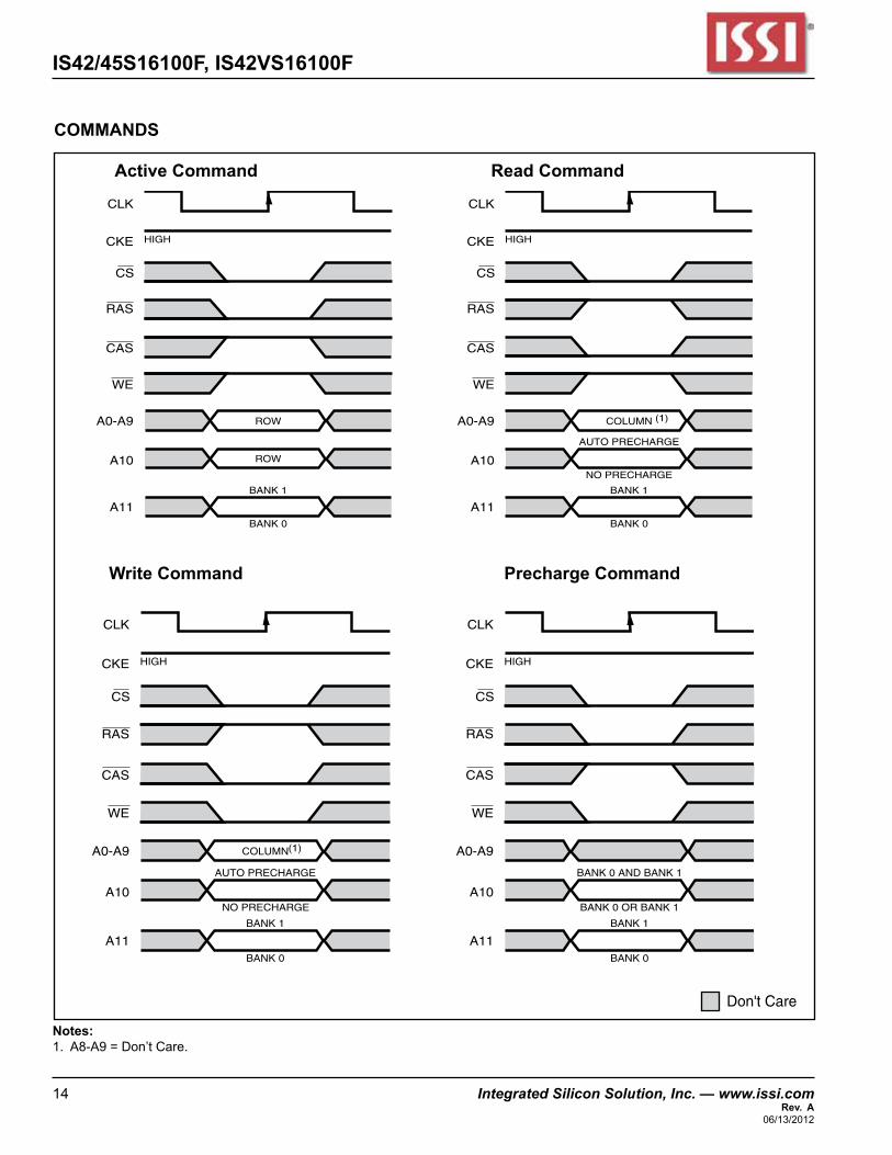
COMMANDS
CLK
CKE HIGH
ROW
ROW
BANK 1
BANK 0
CS
RAS
CAS
WE
A0-A9
A10
A11
CLK
CKE HIGH
COLUMN
BANK 1
AUTO PRECHARGE
NO PRECHARGE
BANK 0
CS
RAS
CAS
WE
A0-A9
A10
A11
(1)
CLK
CKE HIGH
COLUMN
AUTO PRECHARGE
BANK 1
BANK 0
CS
RAS
CAS
WE
A0-A9
A10
A11
CLK
CKE HIGH
BANK 1
BANK 0 AND BANK 1
BANK 0 OR BANK 1NO PRECHARGE
BANK 0
CS
RAS
CAS
WE
A0-A9
A10
A11
(1)
Notes:1.A8-A9=Don’tCare.
Don't Care
Active Command Read Command
Write Command Precharge Command
Integrated Silicon Solution, Inc. — www.issi.com 15Rev. A06/13/2012
IS42/45S16100F, IS42VS16100F
COMMANDS (cont.)
CLK
CKE HIGH
CS
RAS
CAS
WE
A0-A9
A10
A11
CLK
CKE HIGH
CS
RAS
CAS
WE
A0-A9
A10
A11
CLK
CKE HIGH
CS
RAS
CAS
WE
A0-A9
A10
A11
CLK
CKE HIGH
CS
RAS
CAS
WE
A0-A9
A10
A11
OP-CODE
OP-CODE
OP-CODE
Don't Care
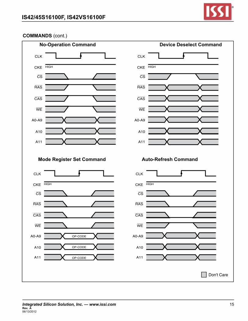
No-Operation Command Device Deselect Command
Mode Register Set Command Auto-Refresh Command
IS42/45S16100F, IS42VS16100F
16 Integrated Silicon Solution, Inc. — www.issi.com Rev. A
06/13/2012
COMMANDS (cont.)
CLK
CKE
CS
RAS
CAS
WE
A0-A9
A10
A11
CLK
CKE
CS
RAS
CAS
WE
A0-A9
A10
A11
BANK(S) ACTIVE HIGH
NOP
NOP
NOP
NOP
CLK
CKE
CS
RAS
CAS
WE
A0-A9
A10
A11
CLK
CKE
CS
RAS
CAS
WE
A0-A9
A10
A11
ALL BANKS IDLE
NOP
NOP
NOP
NOP
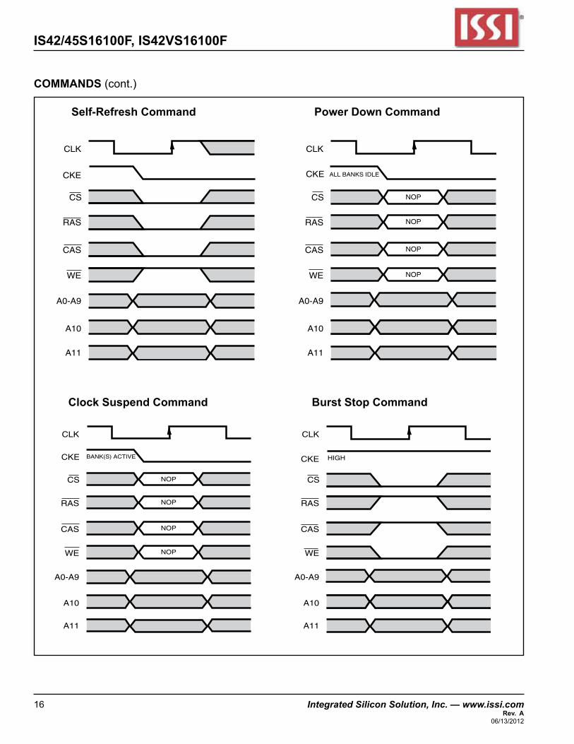
Self-Refresh Command Power Down Command
Clock Suspend Command Burst Stop Command
Integrated Silicon Solution, Inc. — www.issi.com 17Rev. A06/13/2012
IS42/45S16100F, IS42VS16100F
Mode Register Set Command(CS,RAS,CAS,WE=LOW)
The IS42/45S16100F and IS42VS16100F productincorporatesaregisterthatdefinesthedeviceoperatingmode.ThiscommandfunctionsasadatainputpinthatloadsthisregisterfromthepinsA0toA11.Whenpowerisfirstapplied,thestipulatedpower-onsequenceshouldbeexecutedandthentheSDRAMshouldbeinitializedbyexecutingamoderegistersetcommand.
Note that the mode register set command can beexecutedonlywhenbothbanksareintheidlestate(i.e.deactivated).
Another command cannot be executed after a moderegistersetcommanduntilafterthepassageoftheperiodtmcd, whichistheperiodrequiredformoderegistersetcommandexecution.
Active Command (CS,RAS=LOW,CAS,WE=HIGH)
TheSDRAMincludestwobanksof2048rowseach.ThiscommandselectsoneofthetwobanksaccordingtotheA11pinandactivatestherowselectedbythepinsA0toA10.
ThiscommandcorrespondstothefalloftheRASsignalfromHIGHtoLOWinconventionalDRAMs.
Precharge Command (CS,RAS,WE=LOW,CAS=HIGH)
ThiscommandstartsprechargingthebankselectedbypinsA10andA11.WhenA10 isHIGH,bothbanksareprecharged at the same time.WhenA10 is LOW, thebankselectedbyA11isprecharged.Afterexecutingthiscommand, thenext command for theselectedbank(s)isexecutedafterpassageoftheperiodtrp,whichistheperiodrequiredforbankprecharging.
ThiscommandcorrespondstotheRASsignalfromLOWtoHIGHinconventionalDRAMs
Read Command (CS,CAS=LOW,RAS,WE=HIGH)
ThiscommandselectsthebankspecifiedbytheA11pinand starts a burst read operation at the start addressspecifiedbypinsA0toA9.DataisoutputfollowingCASlatency.
Theselectedbankmustbeactivatedbeforeexecutingthiscommand.
WhentheA10pinisHIGH,thiscommandfunctionsasareadwithauto-prechargecommand.Aftertheburstreadcompletes,thebankselectedbypinA11isprecharged.WhentheA10pinisLOW,thebankselectedbytheA11pin remains in the activated state after the burst readcompletes.
Write Command(CS,CAS,WE=LOW,RAS=HIGH)
Whenburstwritemodehasbeenselectedwiththemoderegister set command, this command selects the bankspecifiedbytheA11pinandstartsaburstwriteoperationatthestartaddressspecifiedbypinsA0toA9.ThisfirstdatamustbeinputtotheDQpinsinthecycleinwhichthiscommand.
Theselectedbankmustbeactivatedbeforeexecutingthiscommand.
WhenA10 pin is HIGH, this command functions as awritewithauto-prechargecommand.Aftertheburstwritecompletes,thebankselectedbypinA11isprecharged.WhentheA10pinis low,thebankselectedbytheA11pin remains in the activated state after the burst writecompletes.
Aftertheinputofthelastburstwritedata,theapplicationmustwaitforthewriterecoveryperiod(tdpl,tdal)toelapseaccordingtoCASlatency.
Auto-Refresh Command(CS,RAS,CAS=LOW,WE,CKE=HIGH)
Thiscommandexecutestheauto-refreshoperation.Therowaddressandbanktoberefreshedareautomaticallygeneratedduringthisoperation.
Bothbanksmustbeplacedintheidlestatebeforeexecutingthiscommand.
Thestipulatedperiod(trc)isrequiredforasinglerefreshoperation, and no other commands can be executedduringthisperiod.
Thedevicegoestotheidlestateaftertheinternalrefreshoperationcompletes.
This commandmust be executed at least 2048 timesevery32ms.
This command corresponds to CBR auto-refresh inconventionalDRAMs.
IS42/45S16100F, IS42VS16100F
18 Integrated Silicon Solution, Inc. — www.issi.com Rev. A
06/13/2012
Self-Refresh Command(CS, RAS, CAS, CKE = LOW, WE = HIGH)
This command executes the self-refresh operation. The row address to be refreshed, the bank, and the refresh interval are generated automatically internally during this operation. The self-refresh operation is started by dropping the CKE pin from HIGH to LOW. The self-refresh operation continues as long as the CKE pin remains LOW and there is no need for external control of any other pins. The self-refresh operation is terminated by raising the CKE pin from LOW to HIGH. The next command cannot be executed until the device internal recovery period (trc)has elapsed. After the self-refresh, since it is impossible to determine the address of the last row to be refreshed, an auto-refresh should immediately be performed for all addresses (2048 cycles).
Both banks must be placed in the idle state before executing this command.
Burst Stop Command (CS, WE, = LOW, RAS, CAS = HIGH)
The command forcibly terminates burst read and write operations. When this command is executed during a burst read operation, data output stops after the CAS latency period has elapsed.
No Operation(CS, = LOW, RAS, CAS, WE = HIGH)
This command has no effect on the device.
Device Deselect Command (CS = HIGH)
This command does not select the device for an object of operation. In other words, it performs no operation with respect to the device.
Power-Down Command(CKE = LOW, CS = HIGH)
When both banks are in the idle (inactive) state, or when at least one of the banks is not in the idle (inactive) state, this command can be used to suppress device power dissipation by reducing device internal operations to the minimal level in order to retain data content. Power-down
mode is started by dropping the CKE pin from HIGH to LOW, while satisfying the other command input conditions (see CKE Truth Table). Power-down mode continues as long as the CKE pin is held low. All pins other than the CKE pin are invalid and none of the other commands can be executed in this mode. The power-down operation is terminated by raising the CKE pin from LOW to HIGH. The next command cannot be executed until the recovery period (tcka) has elapsed.
Since this command differs from the self-refresh command described above in that the refresh operation is not performed automatically internally, the refresh operation must be performed within the refresh period (tref). Thus the maximum time that power-down mode can be held is just under the refresh cycle time.
Clock Suspend(CKE = LOW)
This command can be used to stop the device internal clock temporarily during a read or write cycle. Clock suspend mode is started by dropping the CKE pin from HIGH to LOW. Clock suspend mode continues as long as the CKE pin is held LOW. All input pins other than the CKE pin are invalid and none of the other commands can be executed in this mode. Also note that the device internal state is maintained. Clock suspend mode is terminated by raising the CKE pin from LOW to HIGH, at which point device operation restarts. The next command cannot be executed until the recovery period (tcka) has elapsed.
Since this command differs from the self-refresh command described above in that the refresh operation is not performed automatically internally, the refresh operation must be performed within the refresh period (tref). Thus the maximum time that clock suspend mode can be held is just under the refresh cycle time.
Integrated Silicon Solution, Inc. — www.issi.com 19Rev. A06/13/2012
IS42/45S16100F, IS42VS16100F
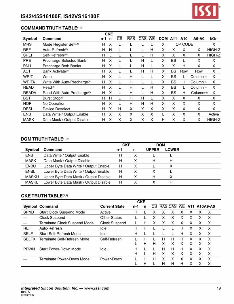
COMMAND TRUTH TABLE(1,2)
CKE Symbol Command n-1 n CS RAS CAS WE DQM A11 A10 A9-A0 I/On
MRS Mode Register Set(3,4) H X L L L L X OP CODE X REF Auto-Refresh(5) H H L L L H X X X X HIGH-Z SREF Self-Refresh(5,6) H L L L L H X X X X HIGH-Z PRE Precharge Selected Bank H X L L H L X BS L X X PALL Precharge Both Banks H X L L H L X X H X X ACT Bank Activate(7) H X L L H H X BS Row Row X WRIT Write H X L H L L X BS L Column(18) X WRITA Write With Auto-Precharge(8) H X L H L L X BS H Column(18) X READ Read(8) H X L H L H X BS L Column(18) X READA Read With Auto-Precharge(8) H X L H L H X BS H Column(18) X BST Burst Stop(9) H H L H H L X X X X X NOP No Operation H X L H H H X X X X X DESL Device Deselect H X H X X X X X X X X ENB Data Write / Output Enable H X X X X X L X X X Active MASK Data Mask / Output Disable H X X X X X H X X X HIGH-Z
DQM TRUTH TABLE(1,2)
CKE DQM Symbol Command n-1 n UPPER LOWER
ENB Data Write / Output Enable H X L L MASK Data Mask / Output Disable H X H H ENBU Upper Byte Data Write / Output Enable H X L X ENBL Lower Byte Data Write / Output Enable H X X L MASKU Upper Byte Data Mask / Output Disable H X H X MASKL Lower Byte Data Mask / Output Disable H X X H
CKE TRUTH TABLE(1,2)
CKE Symbol Command Current State n-1 n CS RAS CAS WE A11 A10 A9-A0
SPND Start Clock Suspend Mode Active H L X X X X X X X — Clock Suspend Other States L L X X X X X X X — Terminate Clock Suspend Mode Clock Suspend L H X X X X X X X REF Auto-Refresh Idle H H L L L H X X X SELF Start Self-Refresh Mode Idle H L L L L H X X X SELFX Terminate Self-Refresh Mode Self-Refresh L H L H H H X X X L H H X X X X X X PDWN Start Power-Down Mode Idle H L L H H H X X X H L H X X X X X X — Terminate Power-Down Mode Power-Down L H H X X X X X X L H L H H H X X X
IS42/45S16100F, IS42VS16100F
20 Integrated Silicon Solution, Inc. — www.issi.com Rev. A
06/13/2012
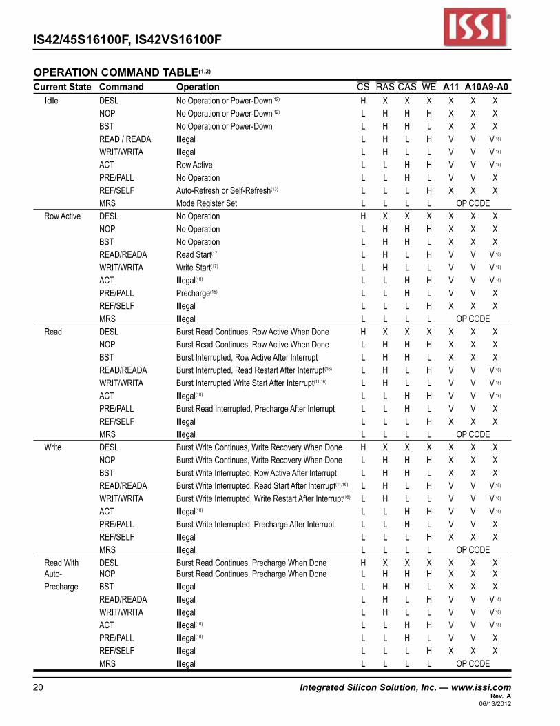
OPERATION COMMAND TABLE(1,2)
Current State Command Operation CS RAS CAS WE A11 A10 A9-A0 Idle DESL NoOperationorPower-Down(12) H X X X X X X NOP NoOperationorPower-Down(12) L H H H X X X BST NoOperationorPower-Down L H H L X X X READ/READA Illegal L H L H V V V(18)
WRIT/WRITA Illegal L H L L V V V(18)
ACT RowActive L L H H V V V(18)
PRE/PALL NoOperation L L H L V V X REF/SELF Auto-RefreshorSelf-Refresh(13) L L L H X X X MRS ModeRegisterSet L L L L OPCODE RowActive DESL NoOperation H X X X X X X NOP NoOperation L H H H X X X BST NoOperation L H H L X X X READ/READA ReadStart(17) L H L H V V V(18)
WRIT/WRITA WriteStart(17) L H L L V V V(18)
ACT Illegal(10) L L H H V V V(18)
PRE/PALL Precharge(15) L L H L V V X REF/SELF Illegal L L L H X X X MRS Illegal L L L L OPCODE Read DESL BurstReadContinues,RowActiveWhenDone H X X X X X X NOP BurstReadContinues,RowActiveWhenDone L H H H X X X BST BurstInterrupted,RowActiveAfterInterrupt L H H L X X X READ/READA BurstInterrupted,ReadRestartAfterInterrupt(16) L H L H V V V(18)
WRIT/WRITA BurstInterruptedWriteStartAfterInterrupt(11,16) L H L L V V V(18)
ACT Illegal(10) L L H H V V V(18)
PRE/PALL BurstReadInterrupted,PrechargeAfterInterrupt L L H L V V X REF/SELF Illegal L L L H X X X MRS Illegal L L L L OPCODE Write DESL BurstWriteContinues,WriteRecoveryWhenDone H X X X X X X NOP BurstWriteContinues,WriteRecoveryWhenDone L H H H X X X BST BurstWriteInterrupted,RowActiveAfterInterrupt L H H L X X X READ/READA BurstWriteInterrupted,ReadStartAfterInterrupt(11,16) L H L H V V V(18)
WRIT/WRITA BurstWriteInterrupted,WriteRestartAfterInterrupt(16) L H L L V V V(18)
ACT Illegal(10) L L H H V V V(18)
PRE/PALL BurstWriteInterrupted,PrechargeAfterInterrupt L L H L V V X REF/SELF Illegal L L L H X X X MRS Illegal L L L L OPCODE ReadWith DESL BurstReadContinues,PrechargeWhenDone H X X X X X X Auto- NOP BurstReadContinues,PrechargeWhenDone L H H H X X X Precharge BST Illegal L H H L X X X READ/READA Illegal L H L H V V V(18)
WRIT/WRITA Illegal L H L L V V V(18)
ACT Illegal(10) L L H H V V V(18)
PRE/PALL Illegal(10) L L H L V V X REF/SELF Illegal L L L H X X X MRS Illegal L L L L OPCODE
Integrated Silicon Solution, Inc. — www.issi.com 21Rev. A06/13/2012
IS42/45S16100F, IS42VS16100F
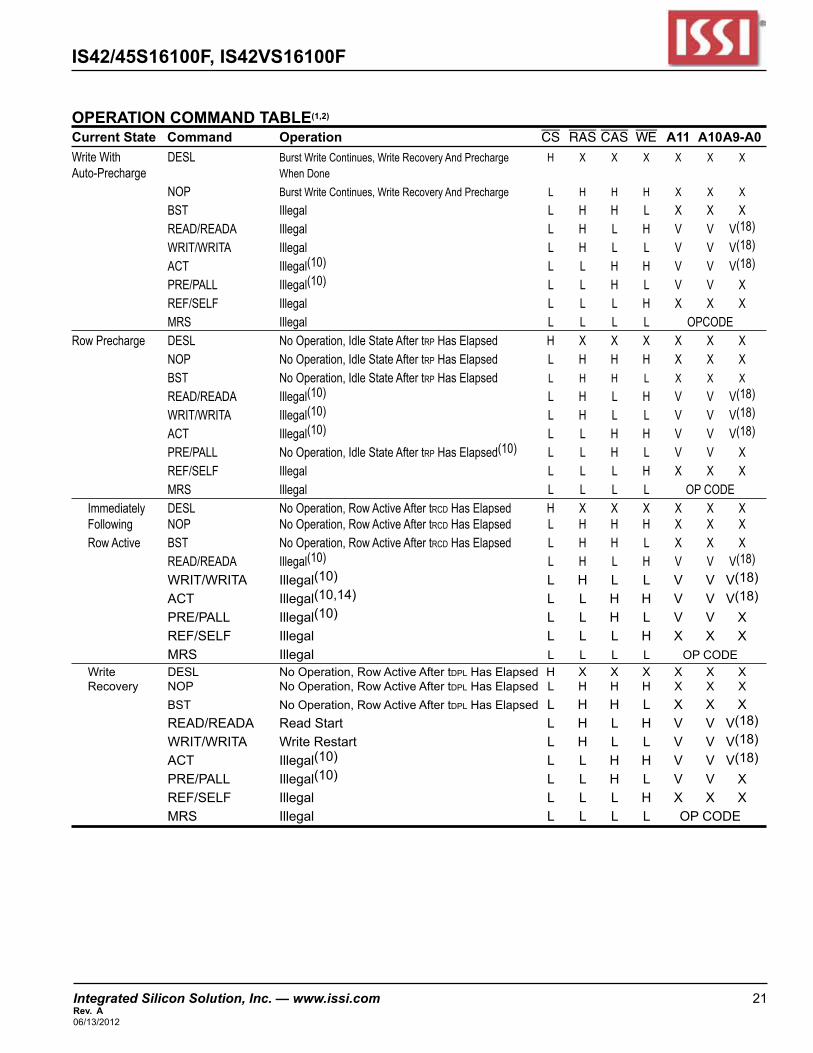
OPERATION COMMAND TABLE(1,2)
Current State Command Operation CS RAS CAS WE A11 A10 A9-A0 WriteWith DESL BurstWriteContinues,WriteRecoveryAndPrecharge H X X X X X XAuto-Precharge WhenDone NOP BurstWriteContinues,WriteRecoveryAndPrecharge L H H H X X X BST Illegal L H H L X X X READ/READA Illegal L H L H V V V(18) WRIT/WRITA Illegal L H L L V V V(18) ACT Illegal(10) L L H H V V V(18) PRE/PALL Illegal(10) L L H L V V X REF/SELF Illegal L L L H X X X MRS Illegal L L L L OPCODERowPrecharge DESL NoOperation,IdleStateAftertrpHasElapsed H X X X X X X NOP NoOperation,IdleStateAftertrp HasElapsed L H H H X X X BST NoOperation,IdleStateAftertrpHasElapsed L H H L X X X READ/READA Illegal(10) L H L H V V V(18) WRIT/WRITA Illegal(10) L H L L V V V(18) ACT Illegal(10) L L H H V V V(18) PRE/PALL NoOperation,IdleStateAftertrpHasElapsed(10) L L H L V V X REF/SELF Illegal L L L H X X X MRS Illegal L L L L OPCODE Immediately DESL NoOperation,RowActiveAftertrcdHasElapsed H X X X X X X Following NOP NoOperation,RowActiveAftertrcdHasElapsed L H H H X X X RowActive BST NoOperation,RowActiveAftertrcdHasElapsed L H H L X X X READ/READA Illegal(10) L H L H V V V(18) WRIT/WRITA Illegal(10) L H L L V V V(18) ACT Illegal(10,14) L L H H V V V(18) PRE/PALL Illegal(10) L L H L V V X REF/SELF Illegal L L L H X X X MRS Illegal L L L L OPCODE Write DESL NoOperation,RowActiveAftertdpl HasElapsed H X X X X X X Recovery NOP NoOperation,RowActiveAftertdpl HasElapsed L H H H X X X BST NoOperation,RowActiveAftertdplHasElapsed L H H L X X X READ/READA ReadStart L H L H V V V(18) WRIT/WRITA WriteRestart L H L L V V V(18) ACT Illegal(10) L L H H V V V(18) PRE/PALL Illegal(10) L L H L V V X REF/SELF Illegal L L L H X X X MRS Illegal L L L L OPCODE
IS42/45S16100F, IS42VS16100F
22 Integrated Silicon Solution, Inc. — www.issi.com Rev. A
06/13/2012
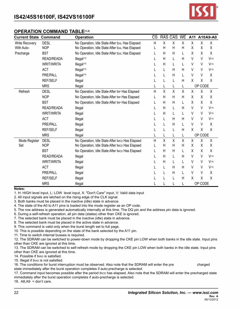
OPERATION COMMAND TABLE(1,2)
Current State Command Operation CS RAS CAS WE A11 A10 A9-A0 WriteRecovery DESL NoOperation,IdleStateAftertdalHasElapsed H X X X X X XWithAuto- NOP NoOperation,IdleStateAftertdalHasElapsed L H H H X X XPrecharge BST NoOperation,IdleStateAftertdalHasElapsed L H H L X X X READ/READA Illegal(10) L H L H V V V(18)
WRIT/WRITA Illegal(10) L H L L V V V(18)
ACT Illegal(10) L L H H V V V(18)
PRE/PALL Illegal(10) L L H L V V X REF/SELF Illegal L L L H X X X MRS Illegal L L L L OPCODE Refresh DESL NoOperation,IdleStateAftertrp HasElapsed H X X X X X X NOP NoOperation,IdleStateAftertrpHasElapsed L H H H X X X BST NoOperation,IdleStateAftertrpHasElapsed L H H L X X X READ/READA Illegal L H L H V V V(18)
WRIT/WRITA Illegal L H L L V V V(18)
ACT Illegal L L H H V V V(18)
PRE/PALL Illegal L L H L V V X REF/SELF Illegal L L L H X X X MRS Illegal L L L L OPCODE ModeRegister DESL NoOperation,IdleStateAftertmcdHasElapsed H X X X X X X Set NOP NoOperation,IdleStateAftertmcdHasElapsed L H H H X X X BST NoOperation,IdleStateAftertmcdHasElapsed L H H L X X X READ/READA Illegal L H L H V V V(18)
WRIT/WRITA Illegal L H L L V V V(18)
ACT Illegal L L H H V V V(18)
PRE/PALL Illegal L L H L V V X REF/SELF Illegal L L L H X X X MRS Illegal L L L L OPCODENotes:1.H:HIGHlevelinput,L:LOWlevelinput,X:"Don'tCare"input,V:Validdatainput2.AllinputsignalsarelatchedontherisingedgeoftheCLKsignal.3.Bothbanksmustbeplacedintheinactive(idle)stateinadvance.4.ThestateoftheA0toA11pinsisloadedintothemoderegisterasanOPcode.5.Therowaddressisgeneratedautomaticallyinternallyatthistime.TheDQpinandtheaddresspindataisignored.6.Duringaself-refreshoperation,allpindata(states)otherthanCKEisignored.7.Theselectedbankmustbeplacedintheinactive(idle)stateinadvance.8.Theselectedbankmustbeplacedintheactivestateinadvance.9.Thiscommandisvalidonlywhentheburstlengthsettofullpage.10.ThisispossibledependingonthestateofthebankselectedbytheA11pin.11.Timetoswitchinternalbussesisrequired.12.TheSDRAMcanbeswitchedtopower-downmodebydroppingtheCKEpinLOWwhenbothbanksintheidlestate.InputpinsotherthanCKEareignoredatthistime.13.TheSDRAMcanbeswitchedtoself-refreshmodebydroppingtheCKEpinLOWwhenbothbanksintheidlestate.InputpinsotherthanCKEareignoredatthistime.14.Possibleiftrrdissatisfied.15.Illegaliftrasisnotsatisfied.16.Theconditionsforburstinterruptionmustbeobserved.AlsonotethattheSDRAMwillenterthepre chargedstateimmediatelyaftertheburstoperationcompletesifauto-prechargeisselected.17.Commandinputbecomespossibleaftertheperiodtrcd haselapsed.AlsonotethattheSDRAMwillentertheprechargedstateimmediatelyaftertheburstoperationcompletesifauto-prechargeisselected.18.A8,A9=don’tcare.
Integrated Silicon Solution, Inc. — www.issi.com 23Rev. A06/13/2012
IS42/45S16100F, IS42VS16100F
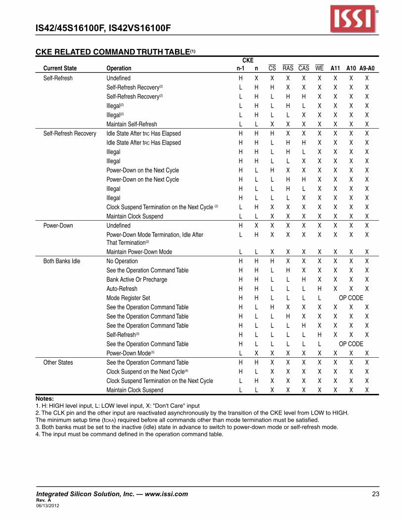
CKE RELATED COMMAND TRUTH TABLE(1)
CKE Current State Operation n-1 n CS RAS CAS WE A11 A10 A9-A0
Self-Refresh Undefined H X X X X X X X X Self-Refresh Recovery(2) L H H X X X X X X Self-Refresh Recovery(2) L H L H H X X X X Illegal(2) L H L H L X X X X Illegal(2) L H L L X X X X X Maintain Self-Refresh L L X X X X X X X Self-Refresh Recovery Idle State After trc Has Elapsed H H H X X X X X X Idle State After trc Has Elapsed H H L H H X X X X Illegal H H L H L X X X X Illegal H H L L X X X X X Power-Down on the Next Cycle H L H X X X X X X Power-Down on the Next Cycle H L L H H X X X X Illegal H L L H L X X X X Illegal H L L L X X X X X Clock Suspend Termination on the Next Cycle (2) L H X X X X X X X Maintain Clock Suspend L L X X X X X X X Power-Down Undefined H X X X X X X X X Power-Down Mode Termination, Idle After L H X X X X X X X That Termination(2)
Maintain Power-Down Mode L L X X X X X X X Both Banks Idle No Operation H H H X X X X X X See the Operation Command Table H H L H X X X X X Bank Active Or Precharge H H L L H X X X X Auto-Refresh H H L L L H X X X Mode Register Set H H L L L L OP CODE See the Operation Command Table H L H X X X X X X See the Operation Command Table H L L H X X X X X See the Operation Command Table H L L L H X X X X Self-Refresh(3) H L L L L H X X X See the Operation Command Table H L L L L L OP CODE Power-Down Mode(3) L X X X X X X X X Other States See the Operation Command Table H H X X X X X X X Clock Suspend on the Next Cycle(4) H L X X X X X X X Clock Suspend Termination on the Next Cycle L H X X X X X X X Maintain Clock Suspend L L X X X X X X XNotes: 1. H: HIGH level input, L: LOW level input, X: "Don't Care" input2. The CLK pin and the other input are reactivated asynchronously by the transition of the CKE level from LOW to HIGH. The minimum setup time (tcka) required before all commands other than mode termination must be satisfied.3. Both banks must be set to the inactive (idle) state in advance to switch to power-down mode or self-refresh mode.4. The input must be command defined in the operation command table.
IS42/45S16100F, IS42VS16100F
24 Integrated Silicon Solution, Inc. — www.issi.com Rev. A
06/13/2012
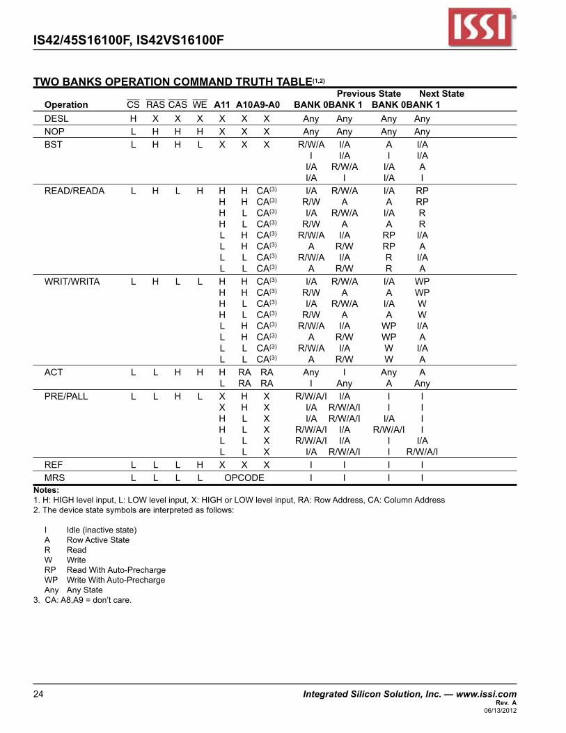
TWO BANKS OPERATION COMMAND TRUTH TABLE(1,2)
Previous State Next State Operation CS RAS CAS WE A11 A10 A9-A0 BANK 0 BANK 1 BANK 0 BANK 1 DESL H X X X X X X Any Any Any Any NOP L H H H X X X Any Any Any Any BST L H H L X X X R/W/A I/A A I/A I I/A I I/A I/A R/W/A I/A A I/A I I/A I READ/READA L H L H H H CA(3) I/A R/W/A I/A RP H H CA(3) R/W A A RP H L CA(3) I/A R/W/A I/A R H L CA(3) R/W A A R L H CA(3) R/W/A I/A RP I/A L H CA(3) A R/W RP A L L CA(3) R/W/A I/A R I/A L L CA(3) A R/W R A WRIT/WRITA L H L L H H CA(3) I/A R/W/A I/A WP H H CA(3) R/W A A WP H L CA(3) I/A R/W/A I/A W H L CA(3) R/W A A W L H CA(3) R/W/A I/A WP I/A L H CA(3) A R/W WP A L L CA(3) R/W/A I/A W I/A L L CA(3) A R/W W A ACT L L H H H RA RA Any I Any A L RA RA I Any A Any PRE/PALL L L H L X H X R/W/A/I I/A I I X H X I/A R/W/A/I I I H L X I/A R/W/A/I I/A I H L X R/W/A/I I/A R/W/A/I I L L X R/W/A/I I/A I I/A L L X I/A R/W/A/I I R/W/A/I REF L L L H X X X I I I I MRS L L L L OPCODE I I I INotes:1.H:HIGHlevelinput,L:LOWlevelinput,X:HIGHorLOWlevelinput,RA:RowAddress,CA:ColumnAddress2.Thedevicestatesymbolsareinterpretedasfollows:
I Idle(inactivestate) A RowActiveState R Read W Write RP ReadWithAuto-Precharge WP WriteWithAuto-Precharge Any AnyState3.CA:A8,A9=don’tcare.
Integrated Silicon Solution, Inc. — www.issi.com 25Rev. A06/13/2012
IS42/45S16100F, IS42VS16100F
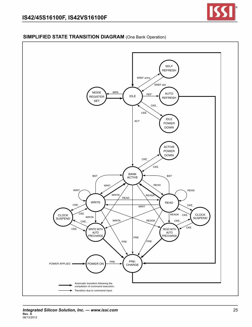
SIMPLIFIED STATE TRANSITION DIAGRAM (OneBankOperation)
SELF
REFRESH
AUTO
REFRESH
IDLE
POWER
DOWN
ACTIVE
POWER
DOWN
IDLEMODE
REGISTER
SET
READ
BANKACTIVE
WRITE
CLOCKSUSPEND
READ WITHAUTO
PRECHARGE
PRE-CHARGEPOWER ON
WRITE WITHAUTO
PRECHARGE
CLOCKSUSPEND
Transition due to command input.
Automatic transition following the completion of command execution.
MRS
SREF entry
SREF exit
REF
CKE_
CKE
ACT
CKE_
CKE
BST BST
READ
CKE_
CKEREADA
CKE_
CKE
READ
READAREAD
WRITA
WRIT
WRIT
CKE_
CKEWRITA
CKE_
CKE
WRIT
WRITA
PRE
PRE
READA
PRE
PRE POWER APPLIED
IS42/45S16100F, IS42VS16100F
26 Integrated Silicon Solution, Inc. — www.issi.com Rev. A
06/13/2012
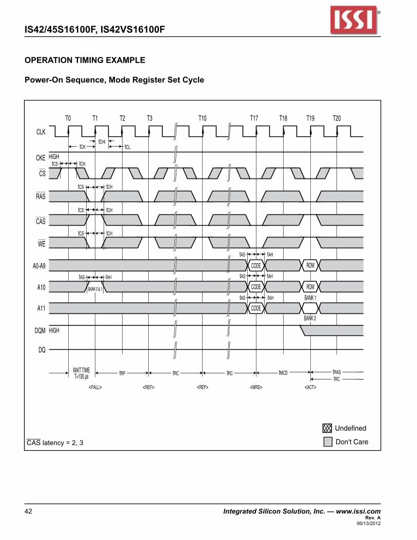
Device Initialization At Power-On(Power-OnSequence)
As is the casewith conventional DRAMs, the SDRAMproductmustbeinitializedbyexecutingastipulatedpower-onsequenceafterpowerisapplied.
Afterpower isappliedandVddandVddQreach theirstipulatedvoltages,setandholdtheCKEandDQMpinsHIGHfor100µs.Then,executetheprechargecommandtoprechargebothbank.Next,execute theauto-refreshcommandtwiceormoreanddefinethedeviceoperationmodebyexecutingamoderegistersetcommand.
Themoderegistersetcommandcanbealsosetbeforeauto-refreshcommand.
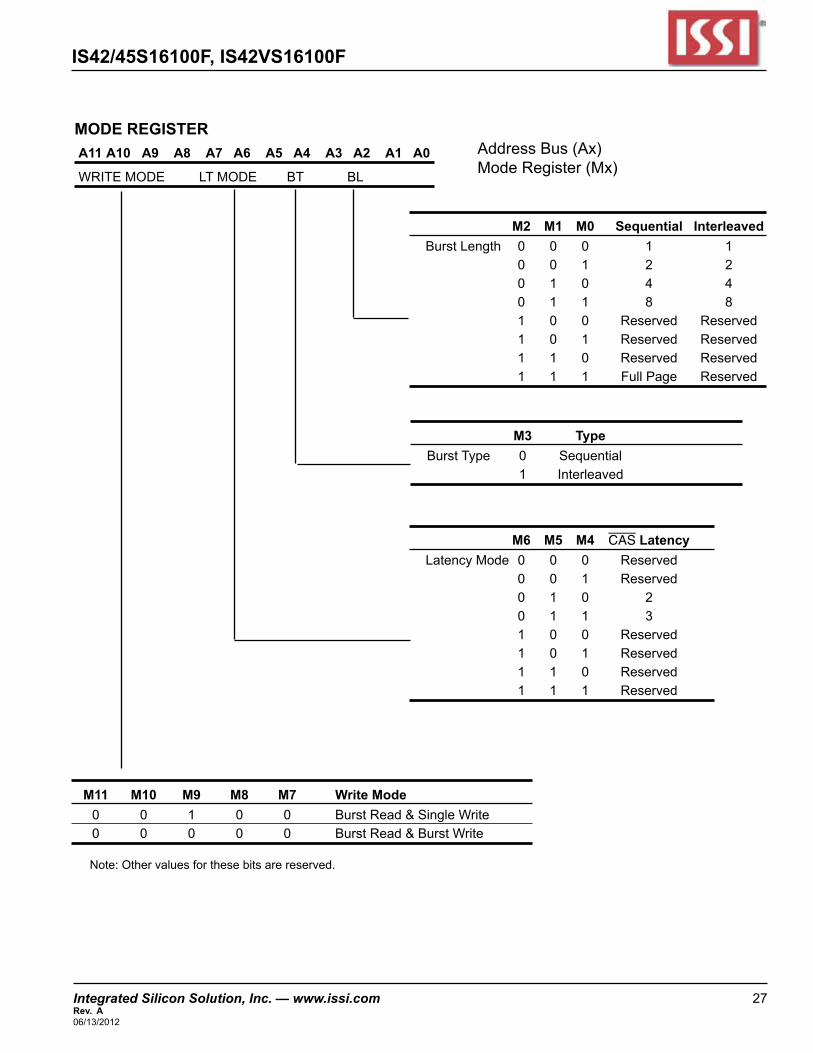
Mode Register Settings Themoderegistersetcommandsetsthemoderegister.Whenthiscommandisexecuted,pinsA0toA9,A10,andA11functionasdatainputpinsforsettingtheregister,andthisdatabecomesthedeviceinternalOPcode.ThisOPcodehasfourfieldsaslistedinthetablebelow.
Notethatthemoderegistersetcommandcanbeexecutedonlywhenbothbanksareintheidle(inactive)state.Waitat least twocyclesafter executingamode register setcommandbeforeexecutingthenextcommand.
CAS LatencyDuringareadoperation,thebetweentheexecutionofthereadcommandanddataoutputisstipulatedastheCASlatency.Thisperiodcanbesetusingthemoderegisterset command. The optimalCAS latency is determinedbytheclockfrequencyanddevicespeedgrade.Seethe“OperatingFrequency/LatencyRelationships”itemfordetailson therelationshipbetweentheclock frequencyandtheCASlatency.Seethetableonthenextpagefordetailsonsettingthemoderegister.
Input Pin Field A11,A10,A9,A8,A7 ModeOptions A6,A5,A4 CASLatency A3 BurstType A2,A1,A0 BurstLength
Burst LengthWhenwritingorreading,datacanbeinputoroutputdatacontinuously.Intheseoperations,anaddressisinputonlyonceandthataddress is takenasthestartingaddressinternally by thedevice.Thedevice thenautomaticallygenerates the followingaddress.Theburst lengthfieldinthemoderegisterstipulatesthenumberofdataitemsinputoroutput in sequence. In theSDRAMproduct,aburst lengthof1,2,4,8,or fullpagecanbespecified.Seethetableonthenextpagefordetailsonsettingthemoderegister.
Burst TypeTheburstdataorderduringareadorwriteoperationisstipulatedbythebursttype,whichcanbesetbythemoderegister set command. The SDRAM product supportssequentialmodeandinterleavedmodebursttypesettings.Seethetableonthenextpagefordetailsonsettingthemoderegister.Seethe“BurstLengthandColumnAddressSequence” item fordetailsonDQdataorders in thesemodes.
Write ModeBurstwriteorsinglewritemodeisselectedbytheOPcode(A11,A10,A9)ofthemoderegister.
AburstwriteoperationisenabledbysettingtheOPcode(A11,A10,A9)to(0,0,0).Aburstwritestartsonthesamecycleasawritecommandset.Thewritestartaddressisspecifiedbythecolumnaddressandbankselectaddressatthewritecommandsetcycle.
AsinglewriteoperationisenabledbysettingOPcode(A11,A10,A9)to(0,0,1).Inasinglewriteoperation,dataisonlywrittentothecolumnaddressandbankselectaddressspecifiedbythewritecommandsetcyclewithoutregardtothebustlengthsetting.
Integrated Silicon Solution, Inc. — www.issi.com 27Rev. A06/13/2012
IS42/45S16100F, IS42VS16100F
MODE REGISTER
M2 M1 M0 Sequential Interleaved BurstLength 0 0 0 1 1 0 0 1 2 2 0 1 0 4 4 0 1 1 8 8 1 0 0 Reserved Reserved 1 0 1 Reserved Reserved 1 1 0 Reserved Reserved 1 1 1 FullPage Reserved
A11 A10 A9 A8 A7 A6 A5 A4 A3 A2 A1 A0
WRITEMODE LTMODE BT BL
M3 Type BurstType 0 Sequential 1 Interleaved
M6 M5 M4 CAS Latency LatencyMode 0 0 0 Reserved 0 0 1 Reserved 0 1 0 2 0 1 1 3 1 0 0 Reserved 1 0 1 Reserved 1 1 0 Reserved 1 1 1 Reserved
M11 M10 M9 M8 M7 Write Mode 0 0 1 0 0 BurstRead&SingleWrite 0 0 0 0 0 BurstRead&BurstWrite
AddressBus(Ax)ModeRegister(Mx)
Note:Othervaluesforthesebitsarereserved.
IS42/45S16100F, IS42VS16100F
28 Integrated Silicon Solution, Inc. — www.issi.com Rev. A
06/13/2012
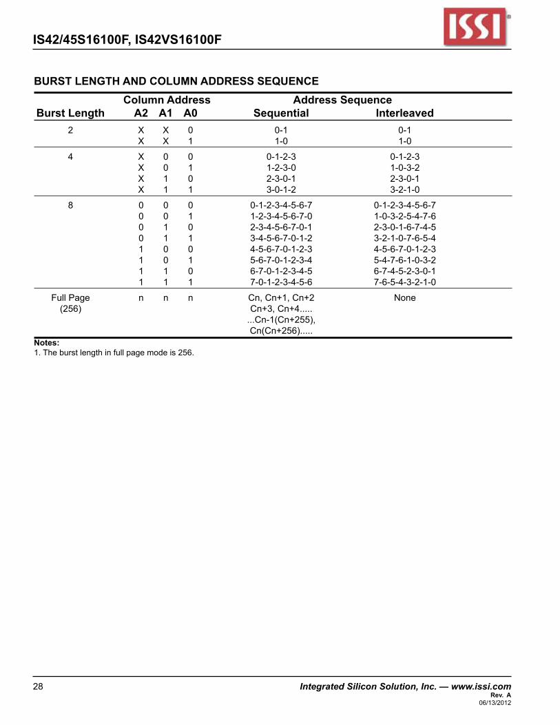
BURST LENGTH AND COLUMN ADDRESS SEQUENCE Column Address Address Sequence Burst Length A2 A1 A0 Sequential Interleaved 2 X X 0 0-1 0-1 X X 1 1-0 1-0
4 X 0 0 0-1-2-3 0-1-2-3 X 0 1 1-2-3-0 1-0-3-2 X 1 0 2-3-0-1 2-3-0-1 X 1 1 3-0-1-2 3-2-1-0
8 0 0 0 0-1-2-3-4-5-6-7 0-1-2-3-4-5-6-7 0 0 1 1-2-3-4-5-6-7-0 1-0-3-2-5-4-7-6 0 1 0 2-3-4-5-6-7-0-1 2-3-0-1-6-7-4-5 0 1 1 3-4-5-6-7-0-1-2 3-2-1-0-7-6-5-4 1 0 0 4-5-6-7-0-1-2-3 4-5-6-7-0-1-2-3 1 0 1 5-6-7-0-1-2-3-4 5-4-7-6-1-0-3-2 1 1 0 6-7-0-1-2-3-4-5 6-7-4-5-2-3-0-1 1 1 1 7-0-1-2-3-4-5-6 7-6-5-4-3-2-1-0
FullPage n n n Cn,Cn+1,Cn+2 None (256) Cn+3,Cn+4..... ...Cn-1(Cn+255), Cn(Cn+256).....Notes:1.Theburstlengthinfullpagemodeis256.
Integrated Silicon Solution, Inc. — www.issi.com 29Rev. A06/13/2012
IS42/45S16100F, IS42VS16100F
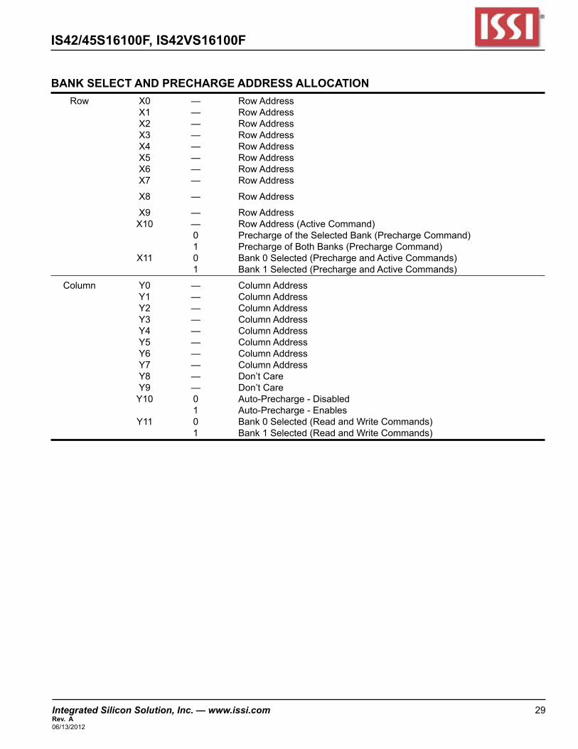
BANK SELECT AND PRECHARGE ADDRESS ALLOCATION Row X0 — RowAddress X1 — RowAddress X2 — RowAddress X3 — RowAddress X4 — RowAddress X5 — RowAddress X6 — RowAddress X7 — RowAddress
X8 — RowAddress
X9 — RowAddress X10 — RowAddress(ActiveCommand) 0 PrechargeoftheSelectedBank(PrechargeCommand) 1 PrechargeofBothBanks(PrechargeCommand) X11 0 Bank0Selected(PrechargeandActiveCommands) 1 Bank1Selected(PrechargeandActiveCommands)
Column Y0 — ColumnAddress Y1 — ColumnAddress Y2 — ColumnAddress Y3 — ColumnAddress Y4 — ColumnAddress Y5 — ColumnAddress Y6 — ColumnAddress Y7 — ColumnAddress Y8 — Don’tCare Y9 — Don’tCare Y10 0 Auto-Precharge-Disabled 1 Auto-Precharge-Enables Y11 0 Bank0Selected(ReadandWriteCommands) 1 Bank1Selected(ReadandWriteCommands)
IS42/45S16100F, IS42VS16100F
30 Integrated Silicon Solution, Inc. — www.issi.com Rev. A
06/13/2012
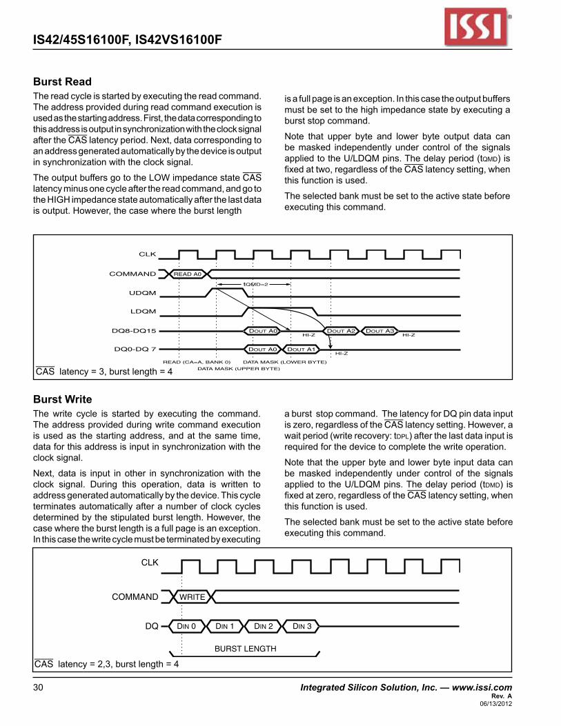
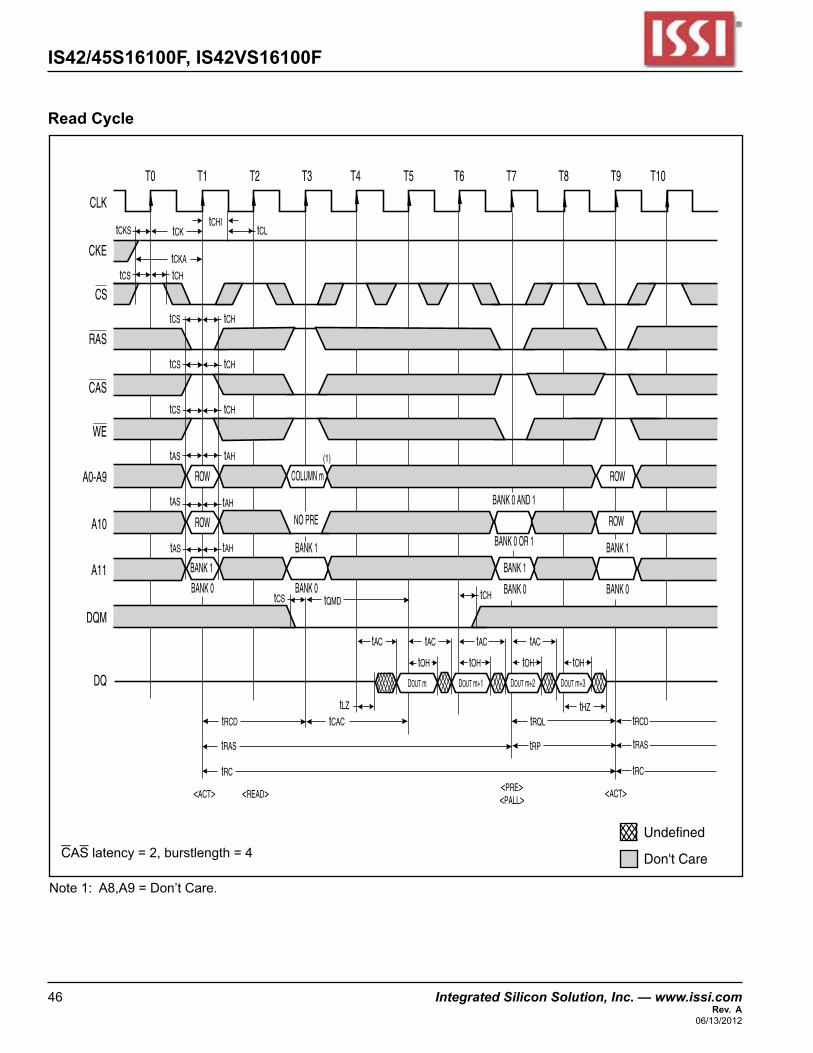
Burst ReadThereadcycleisstartedbyexecutingthereadcommand.Theaddressprovidedduringreadcommandexecutionisusedasthestartingaddress.First,thedatacorrespondingtothisaddressisoutputinsynchronizationwiththeclocksignalaftertheCASlatencyperiod.Next,datacorrespondingtoanaddressgeneratedautomaticallybythedeviceisoutputinsynchronizationwiththeclocksignal.
TheoutputbuffersgototheLOWimpedancestateCASlatencyminusonecycleafterthereadcommand,andgototheHIGHimpedancestateautomaticallyafterthelastdataisoutput.However,thecasewheretheburstlength
isafullpageisanexception.Inthiscasetheoutputbuffersmustbesettothehighimpedancestatebyexecutingaburststopcommand.
Note that upper byte and lower byte output data canbemasked independentlyunder control of thesignalsappliedtotheU/LDQMpins.Thedelayperiod(tqmd)isfixedattwo,regardlessoftheCASlatencysetting,whenthisfunctionisused.
Theselectedbankmustbesettotheactivestatebeforeexecutingthiscommand.
CAS latency=3,burstlength=4
Burst WriteThewrite cycle is started by executing the command.Theaddressprovidedduringwritecommandexecutionisusedas thestartingaddress,andat thesametime,dataforthisaddressisinputinsynchronizationwiththeclocksignal.
Next, data is input inother in synchronizationwith theclock signal. During this operation, data is written toaddressgeneratedautomaticallybythedevice.Thiscycleterminatesautomaticallyafteranumberofclockcyclesdeterminedbythestipulatedburstlength.However,thecasewheretheburstlengthisafullpageisanexception.Inthiscasethewritecyclemustbeterminatedbyexecuting
aburststopcommand.ThelatencyforDQpindatainputiszero,regardlessoftheCASlatencysetting.However,awaitperiod(writerecovery:tdpl)afterthelastdatainputisrequiredforthedevicetocompletethewriteoperation.
Notethattheupperbyteandlowerbyteinputdatacanbemasked independently under control of the signalsappliedtotheU/LDQMpins.Thedelayperiod(tdmd) isfixedatzero,regardlessoftheCASlatencysetting,whenthisfunctionisused.
Theselectedbankmustbesettotheactivestatebeforeexecutingthiscommand.
CAS latency=2,3,burstlength=4
READ A0COMMAND
UDQM
LDQM
DQ8-DQ15
DQ0-DQ 7
CLK
DOUT A0
tQMD=2
HI-Z
HI-Z
HI-Z
READ (CA=A, BANK 0) DATA MASK (LOWER BYTE)
DATA MASK (UPPER BYTE)
DOUT A2 DOUT A3
DOUT A1DOUT A0
BURST LENGTH
WRITECOMMAND
DQ
CLK
DIN 0 DIN 1 DIN 2 DIN 3
Integrated Silicon Solution, Inc. — www.issi.com 31Rev. A06/13/2012
IS42/45S16100F, IS42VS16100F
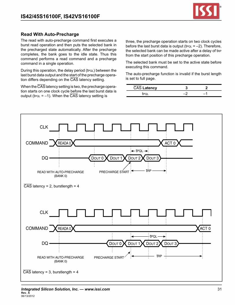
Read With Auto-PrechargeThereadwithauto-prechargecommandfirstexecutesaburstreadoperationandthenputstheselectedbankintheprechargedstateautomatically.After theprechargecompletes, the bank goes to the idle state. Thus thiscommandperformsa readcommandandaprechargecommandinasingleoperation.
Duringthisoperation,thedelayperiod(tpql)betweenthelastburstdataoutputandthestartoftheprechargeopera-tiondiffersdependingontheCASlatencysetting.
WhentheCASlatencysettingistwo,theprechargeopera-tionstartsononeclockcyclebeforethelastburstdataisoutput(tpql=–1).WhentheCASlatencysettingis
three,theprechargeoperationstartsontwoclockcyclesbeforethelastburstdataisoutput(tpql=–2).Therefore,theselectedbankcanbemadeactiveafteradelayoftrpfromthestartpositionofthisprechargeoperation.
Theselectedbankmustbesettotheactivestatebeforeexecutingthiscommand.
Theauto-prechargefunctionisinvalidiftheburstlengthissettofullpage.
CAS Latency 3 2 tpql –2 –1
COMMAND
DQ
CLK
tRP
tPQL
READA 0 ACT 0
PRECHARGE STARTREAD WITH AUTO-PRECHARGE(BANK 0)
DOUT 0 DOUT 1 DOUT 2 DOUT 3
COMMAND
DQ
CLK
READA 0 ACT 0
tRPPRECHARGE STARTREAD WITH AUTO-PRECHARGE(BANK 0)
tPQL
DOUT 0 DOUT 1 DOUT 2 DOUT 3
CASlatency=2,burstlength=4
CAS latency=3,burstlength=4
IS42/45S16100F, IS42VS16100F
32 Integrated Silicon Solution, Inc. — www.issi.com Rev. A
06/13/2012
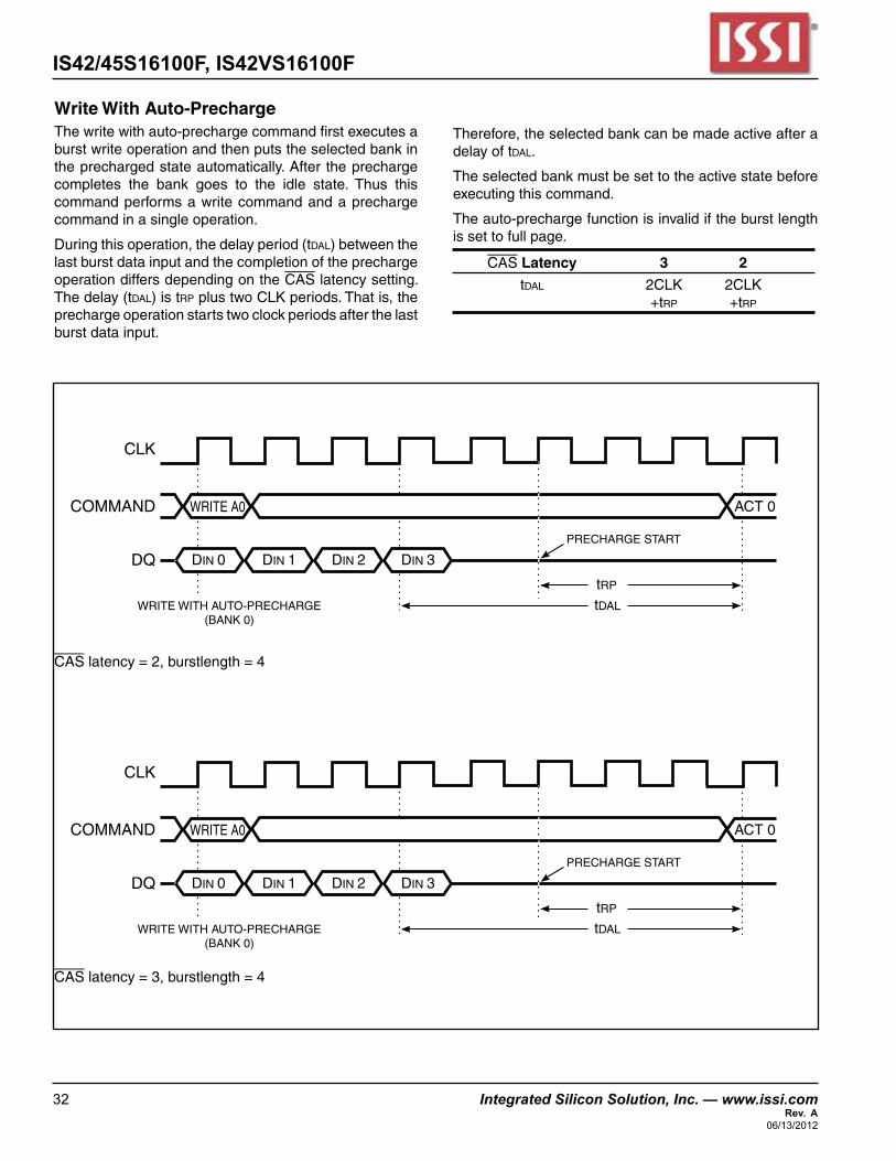
Write With Auto-PrechargeThe write with auto-precharge command first executes a burst write operation and then puts the selected bank in the precharged state automatically. After the precharge completes the bank goes to the idle state. Thus this command performs a write command and a precharge command in a single operation.
During this operation, the delay period (tdal) between the last burst data input and the completion of the precharge operation differs depending on the CAS latency setting. The delay (tdal) is trp plus two CLK periods. That is, the precharge operation starts two clock periods after the last burst data input.
Therefore, the selected bank can be made active after a delay of tdal.
The selected bank must be set to the active state before executing this command.
The auto-precharge function is invalid if the burst length is set to full page.
CAS Latency 3 2
tdal 2CLK 2CLK +trp +trp
tRP
tDAL
PRECHARGE START
DQ
WRITE A0COMMAND
CLK
ACT 0
WRITE WITH AUTO-PRECHARGE(BANK 0)
DIN 0 DIN 1 DIN 2 DIN 3
tRP
tDAL
PRECHARGE START
DQ
WRITE A0COMMAND
CLK
ACT 0
WRITE WITH AUTO-PRECHARGE(BANK 0)
DIN 0 DIN 1 DIN 2 DIN 3
CAS latency = 2, burstlength = 4
CAS latency = 3, burstlength = 4
Integrated Silicon Solution, Inc. — www.issi.com 33Rev. A06/13/2012
IS42/45S16100F, IS42VS16100F
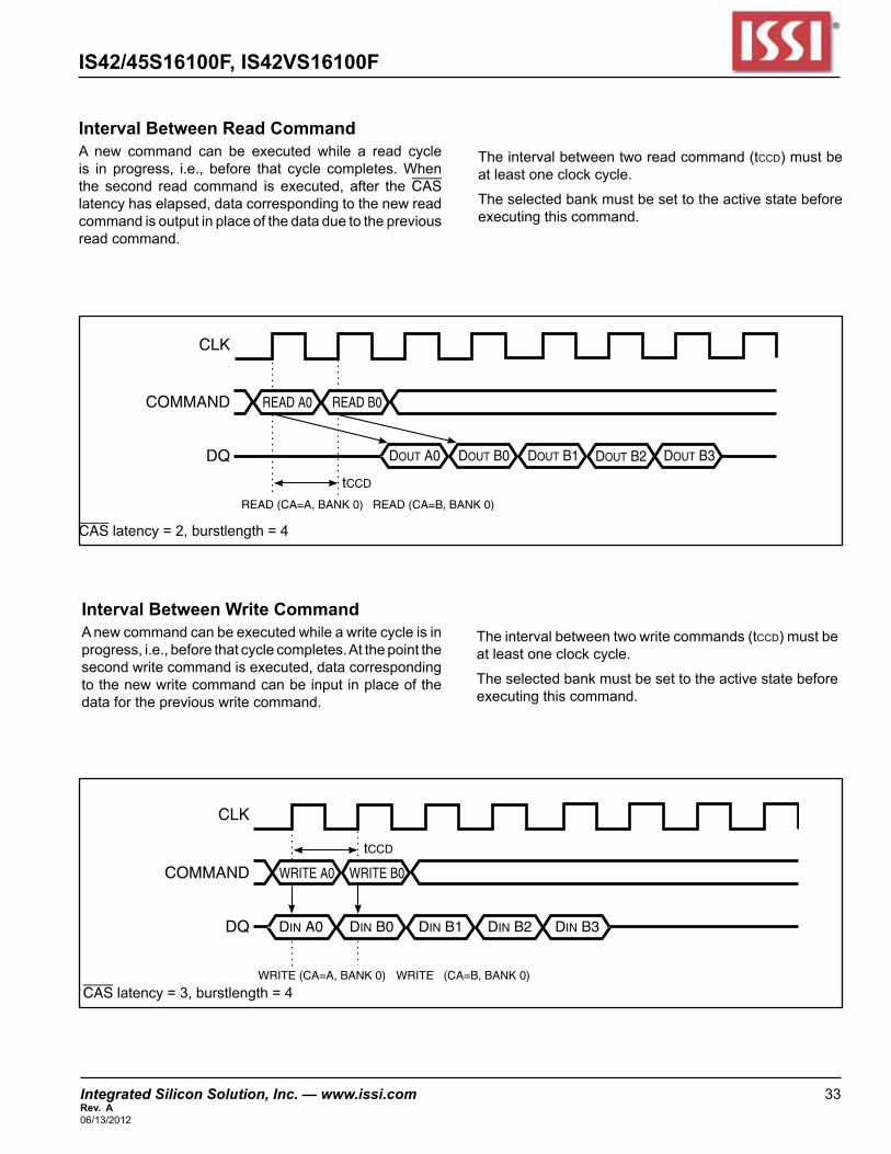
Interval Between Read CommandA new command can be executed while a read cycleis in progress, i.e., before that cycle completes.Whenthe second read command is executed, after theCASlatencyhaselapsed,datacorrespondingtothenewreadcommandisoutputinplaceofthedataduetothepreviousreadcommand.
Theintervalbetweentworeadcommand(tccd)mustbeatleastoneclockcycle.
Theselectedbankmustbesettotheactivestatebeforeexecutingthiscommand.
Interval Between Write CommandAnewcommandcanbeexecutedwhileawritecycleisinprogress,i.e.,beforethatcyclecompletes.Atthepointthesecondwritecommandisexecuted,datacorrespondingtothenewwritecommandcanbeinputinplaceofthedataforthepreviouswritecommand.
Theintervalbetweentwowritecommands(tccd)mustbeatleastoneclockcycle.
Theselectedbankmustbesettotheactivestatebeforeexecutingthiscommand.
READ A0 READ B0COMMAND
DQ
CLK
DOUT A0 DOUT B0 DOUT B1 DOUT B2
READ (CA=A, BANK 0) READ (CA=B, BANK 0)
tCCD
DOUT B3
CASlatency=2,burstlength=4
WRITE A0 WRITE B0COMMAND
DQ
CLK
DIN A0 DIN B0 DIN B1 DIN B2 DIN B3
WRITE (CA=A, BANK 0) WRITE (CA=B, BANK 0)
tCCD
CASlatency=3,burstlength=4
IS42/45S16100F, IS42VS16100F
34 Integrated Silicon Solution, Inc. — www.issi.com Rev. A
06/13/2012
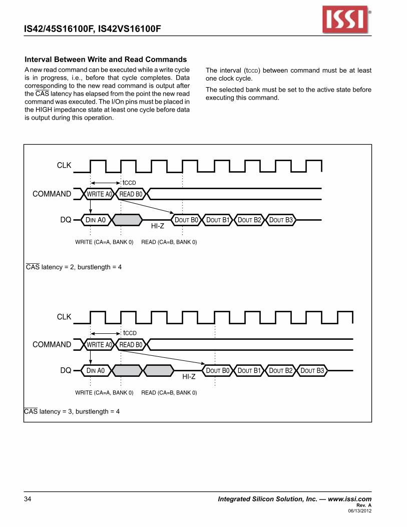
Interval Between Write and Read CommandsAnewreadcommandcanbeexecutedwhileawritecycleis in progress, i.e., before that cycle completes. DatacorrespondingtothenewreadcommandisoutputaftertheCASlatencyhaselapsedfromthepointthenewreadcommandwasexecuted.TheI/OnpinsmustbeplacedintheHIGHimpedancestateatleastonecyclebeforedataisoutputduringthisoperation.
The interval (tccd)betweencommandmustbeat leastoneclockcycle.
Theselectedbankmustbesettotheactivestatebeforeexecutingthiscommand.
DQ
WRITE A0 READ B0COMMAND
CLK
DIN A0 DOUT B0 DOUT B2DOUT B1 DOUT B3
tCCD
HI-Z
WRITE (CA=A, BANK 0) READ (CA=B, BANK 0)
DQ
WRITE A0 READ B0COMMAND
CLK
DIN A0 DOUT B0 DOUT B2DOUT B1 DOUT B3
tCCD
HI-Z
WRITE (CA=A, BANK 0) READ (CA=B, BANK 0)
CASlatency=2,burstlength=4
CASlatency=3,burstlength=4
Integrated Silicon Solution, Inc. — www.issi.com 35Rev. A06/13/2012
IS42/45S16100F, IS42VS16100F
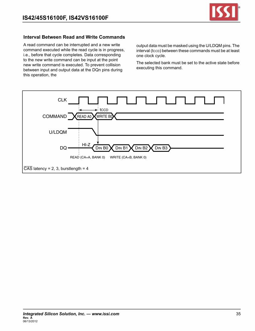
Interval Between Read and Write CommandsAreadcommandcanbeinterruptedandanewwritecommandexecutedwhilethereadcycleisinprogress,i.e.,beforethatcyclecompletes.Datacorrespondingtothenewwritecommandcanbeinputatthepointnewwritecommandisexecuted.TopreventcollisionbetweeninputandoutputdataattheDQnpinsduringthisoperation,the
outputdatamustbemaskedusingtheU/LDQMpins.Theinterval(tccd)betweenthesecommandsmustbeatleastoneclockcycle.
Theselectedbankmustbesettotheactivestatebeforeexecutingthiscommand.
WRITE B0READ A0COMMAND
U/LDQM
DQ
CLK
DIN B0 DIN B2DIN B1 DIN B3
tCCD
HI-Z
READ (CA=A, BANK 0) WRITE (CA=B, BANK 0)
CAS latency=2,3,burstlength=4
IS42/45S16100F, IS42VS16100F
36 Integrated Silicon Solution, Inc. — www.issi.com Rev. A
06/13/2012
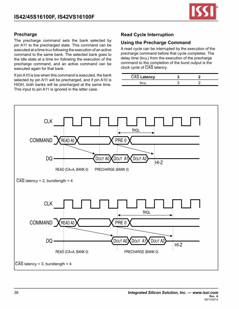
PrechargeThe precharge command sets the bank selected bypinA11totheprechargedstate.Thiscommandcanbeexecutedatatimetras followingtheexecutionofanactivecommandtothesamebank.Theselectedbankgoestotheidlestateatatimetrpfollowingtheexecutionoftheprecharge command, and an active command can beexecutedagainforthatbank.
IfpinA10islowwhenthiscommandisexecuted,thebankselectedbypinA11willbeprecharged,andifpinA10isHIGH,bothbankswillbeprechargedatthesametime.ThisinputtopinA11isignoredinthelattercase.
Read Cycle InterruptionUsing the Precharge CommandAreadcyclecanbeinterruptedbytheexecutionoftheprechargecommandbeforethatcyclecompletes.Thedelaytime(trql)fromtheexecutionoftheprechargecommandtothecompletionoftheburstoutputistheclockcycleofCASlatency.
CAS Latency 3 2 trql 3 2
tRQL
tRQL
PRE 0READ A0COMMAND
DQ
CLK
DOUT A0 DOUT A1 DOUT A2HI-Z
READ (CA=A, BANK 0) PRECHARGE (BANK 0)
PRE 0READ A0COMMAND
DQ
CLK
DOUT A0 DOUT A1 DOUT A2HI-Z
READ (CA=A, BANK 0) PRECHARGE (BANK 0)
CASlatency=2,burstlength=4
CAS latency=3,burstlength=4
Integrated Silicon Solution, Inc. — www.issi.com 37Rev. A06/13/2012
IS42/45S16100F, IS42VS16100F
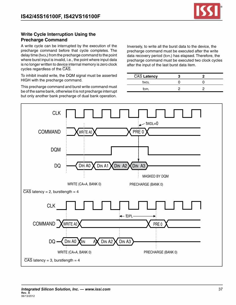
Write Cycle Interruption Using the Precharge CommandA write cycle can be interrupted by the execution of the precharge command before that cycle completes. The delay time (twdl) from the precharge command to the point where burst input is invalid, i.e., the point where input data is no longer written to device internal memory is zero clock cycles regardless of the CAS.
To inhibit invalid write, the DQM signal must be asserted HIGH with the precharge command.
This precharge command and burst write command must be of the same bank, otherwise it is not precharge interrupt but only another bank precharge of dual bank operation.
Inversely, to write all the burst data to the device, the precharge command must be executed after the write data recovery period (tdpl) has elapsed. Therefore, the precharge command must be executed two clock cycles after the input of the last burst data item.
CAS Latency 3 2
twdl 0 0
tdpl 2 2
PRE 0WRITE A0COMMAND
DQM
DQ
CLK
DIN A0 DIN A1 DIN A2 DIN A3
tWDL=0
WRITE (CA=A, BANK 0) PRECHARGE (BANK 0)
MASKED BY DQM
WRITE A0COMMAND
DQ
CLK
DIN A0 DIN A1 DIN A2 DIN A3
tDPL
WRITE (CA=A, BANK 0) PRECHARGE (BANK 0)
PRE 0
CAS latency = 2, burstlength = 4
CAS latency = 3, burstlength = 4
IS42/45S16100F, IS42VS16100F
38 Integrated Silicon Solution, Inc. — www.issi.com Rev. A
06/13/2012
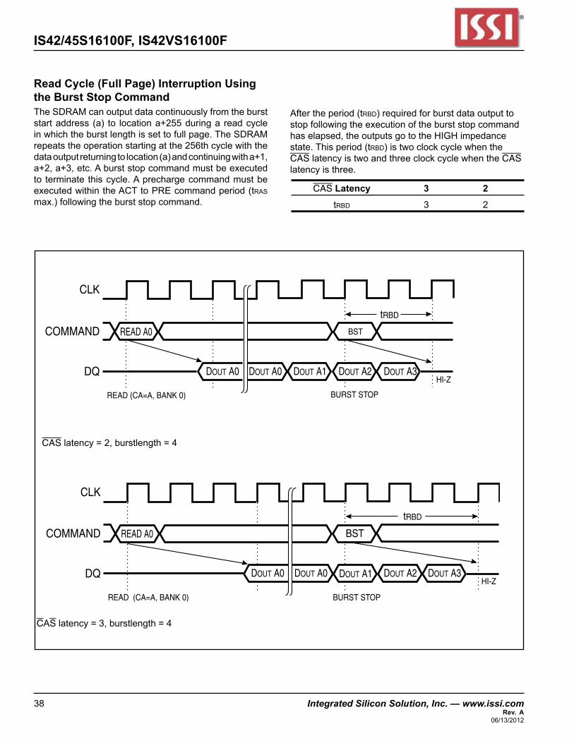
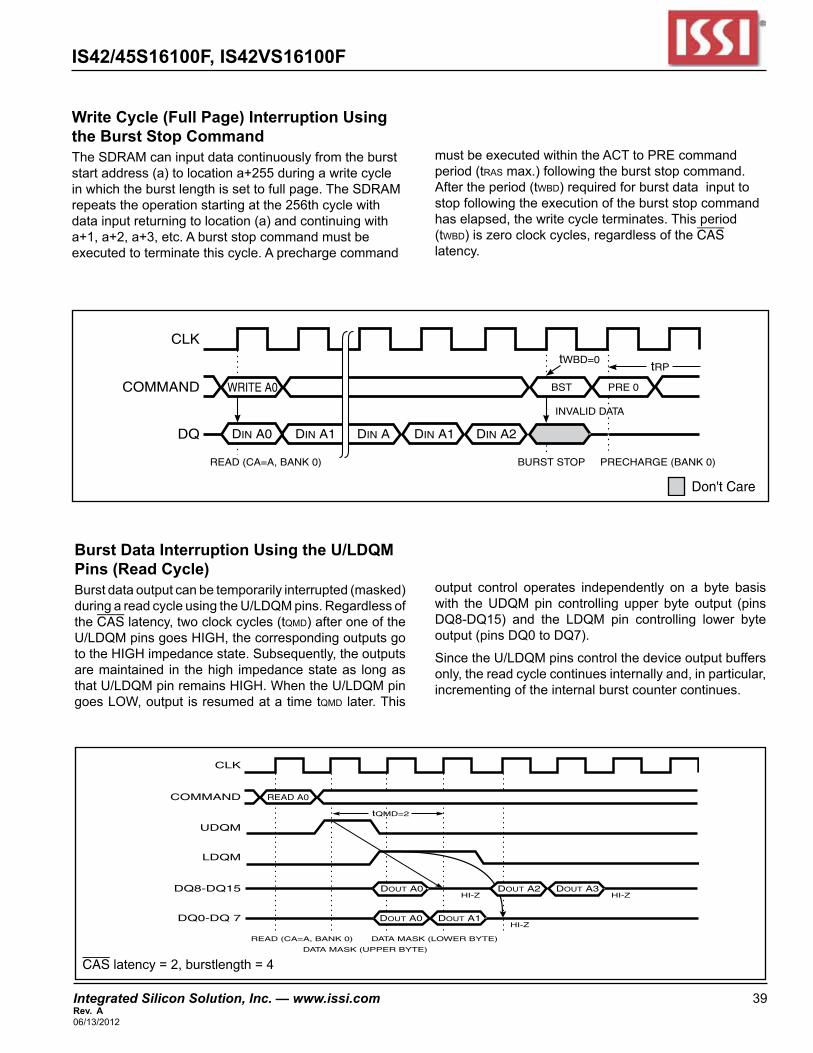
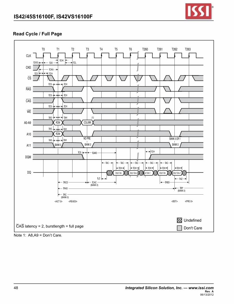
Read Cycle (Full Page) Interruption Using the Burst Stop CommandTheSDRAMcanoutputdatacontinuouslyfromtheburststartaddress(a) to locationa+255duringa readcycleinwhichtheburstlengthissettofullpage.TheSDRAMrepeatstheoperationstartingatthe256thcyclewiththedataoutputreturningtolocation(a)andcontinuingwitha+1,a+2,a+3,etc.Aburststopcommandmustbeexecutedto terminate thiscycle.AprechargecommandmustbeexecutedwithintheACTtoPREcommandperiod(trasmax.)followingtheburststopcommand.
Aftertheperiod(trbd)requiredforburstdataoutputtostopfollowingtheexecutionoftheburststopcommandhaselapsed,theoutputsgototheHIGHimpedancestate.Thisperiod(trbd)istwoclockcyclewhentheCASlatencyistwoandthreeclockcyclewhentheCASlatencyisthree.
CAS Latency 3 2 trbd 3 2
BSTREAD A0COMMAND
DQ
CLK
tRBD
READ (CA=A, BANK 0) BURST STOP
HI-ZDOUT A0 DOUT A0 DOUT A1 DOUT A2
COMMAND
DQ
CLK
tRBD
READ A0
READ (CA=A, BANK 0) BURST STOP
BST
HI-ZDOUT A0 DOUT A0 DOUT A1 DOUT A2 DOUT A3
DOUT A3
CASlatency=3,burstlength=4
CASlatency=2,burstlength=4
Integrated Silicon Solution, Inc. — www.issi.com 39Rev. A06/13/2012
IS42/45S16100F, IS42VS16100F
Write Cycle (Full Page) Interruption Using the Burst Stop CommandTheSDRAMcaninputdatacontinuouslyfromtheburststartaddress(a)tolocationa+255duringawritecycleinwhichtheburstlengthissettofullpage.TheSDRAMrepeatstheoperationstartingatthe256thcyclewithdatainputreturningtolocation(a)andcontinuingwitha+1,a+2,a+3,etc.Aburststopcommandmustbeexecutedtoterminatethiscycle.Aprechargecommand
mustbeexecutedwithintheACTtoPREcommandperiod(trasmax.)followingtheburststopcommand.Aftertheperiod(twbd)requiredforburstdatainputtostopfollowingtheexecutionoftheburststopcommandhaselapsed,thewritecycleterminates.Thisperiod(twbd)iszeroclockcycles,regardlessoftheCASlatency.
Burst Data Interruption Using the U/LDQM Pins (Read Cycle)Burstdataoutputcanbetemporarilyinterrupted(masked)duringareadcycleusingtheU/LDQMpins.RegardlessoftheCASlatency,twoclockcycles(tqmd)afteroneoftheU/LDQMpinsgoesHIGH,thecorrespondingoutputsgototheHIGHimpedancestate.Subsequently,theoutputsaremaintained in thehigh impedancestateas longasthatU/LDQMpinremainsHIGH.WhentheU/LDQMpingoesLOW,outputisresumedatatimetqmd later.This
output control operates independently on a byte basiswith theUDQMpin controlling upper byte output (pinsDQ8-DQ15) and the LDQM pin controlling lower byteoutput(pinsDQ0toDQ7).
SincetheU/LDQMpinscontrolthedeviceoutputbuffersonly,thereadcyclecontinuesinternallyand,inparticular,incrementingoftheinternalburstcountercontinues.
CAS latency=2,burstlength=4
READ A0COMMAND
UDQM
LDQM
DQ8-DQ15
DQ0-DQ 7
CLK
DOUT A0
tQMD=2
HI-Z
HI-Z
HI-Z
READ (CA=A, BANK 0) DATA MASK (LOWER BYTE)
DATA MASK (UPPER BYTE)
DOUT A2 DOUT A3
DOUT A1DOUT A0
WRITE A0COMMAND
DQ
CLK
DIN A0 DIN A1 DIN A DIN A1 DIN A2
tWBD=0tRP
READ (CA=A, BANK 0) BURST STOP
BST PRE 0
INVALID DATA
PRECHARGE (BANK 0)
Don't Care
IS42/45S16100F, IS42VS16100F
40 Integrated Silicon Solution, Inc. — www.issi.com Rev. A
06/13/2012
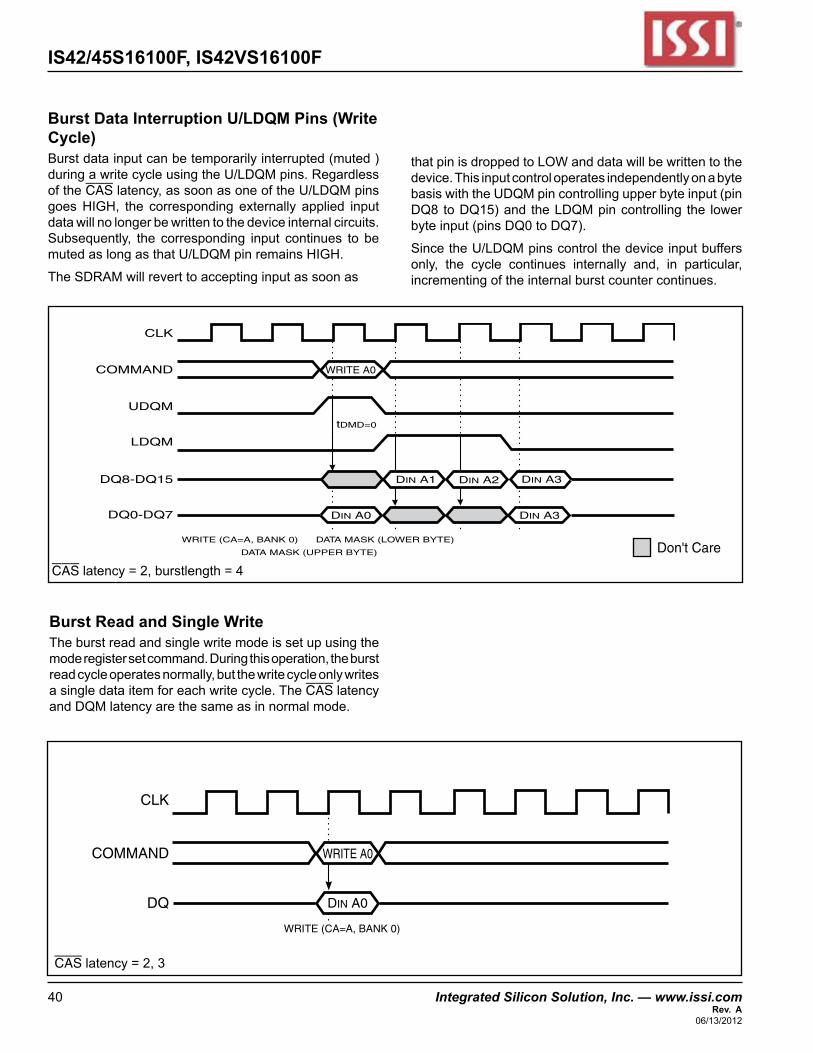
Burst Data Interruption U/LDQM Pins (Write Cycle)Burstdatainputcanbetemporarilyinterrupted(muted)duringawritecycleusingtheU/LDQMpins.RegardlessoftheCASlatency,assoonasoneoftheU/LDQMpinsgoesHIGH, the corresponding externally applied inputdatawillnolongerbewrittentothedeviceinternalcircuits.Subsequently, the corresponding input continues to bemutedaslongasthatU/LDQMpinremainsHIGH.
TheSDRAMwillreverttoacceptinginputassoonas
thatpinisdroppedtoLOWanddatawillbewrittentothedevice.ThisinputcontroloperatesindependentlyonabytebasiswiththeUDQMpincontrollingupperbyteinput(pinDQ8toDQ15)and theLDQMpincontrolling the lowerbyteinput(pinsDQ0toDQ7).
SincetheU/LDQMpinscontrolthedeviceinputbuffersonly, the cycle continues internally and, in particular,incrementingoftheinternalburstcountercontinues.
Burst Read and Single WriteTheburstreadandsinglewritemodeissetupusingthemoderegistersetcommand.Duringthisoperation,theburstreadcycleoperatesnormally,butthewritecycleonlywritesasingledataitemforeachwritecycle.TheCASlatencyandDQMlatencyarethesameasinnormalmode.
WRITE A0COMMAND
UDQM
LDQM
DQ8-DQ15
DQ0-DQ7
CLK
DIN A1
WRITE (CA=A, BANK 0) DATA MASK (LOWER BYTE)
DATA MASK (UPPER BYTE)
tDMD=0
DIN A2 DIN A3
DIN A0 DIN A3
Don't Care
CASlatency=2,3
CASlatency=2,burstlength=4
WRITE A0COMMAND
DQ
CLK
DIN A0
WRITE (CA=A, BANK 0)
Integrated Silicon Solution, Inc. — www.issi.com 41Rev. A06/13/2012
IS42/45S16100F, IS42VS16100F
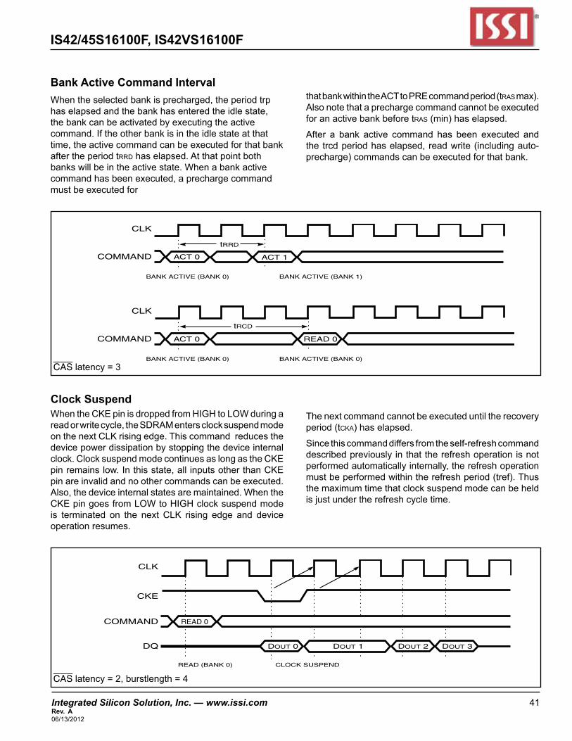
Bank Active Command IntervalWhentheselectedbankisprecharged,theperiodtrphaselapsedandthebankhasenteredtheidlestate,thebankcanbeactivatedbyexecutingtheactivecommand.Iftheotherbankisintheidlestateatthattime,theactivecommandcanbeexecutedforthatbankaftertheperiodtrrdhaselapsed.Atthatpointbothbankswillbeintheactivestate.Whenabankactivecommandhasbeenexecuted,aprechargecommandmustbeexecutedfor
thatbankwithintheACTtoPREcommandperiod(trasmax).Alsonotethataprechargecommandcannotbeexecutedforanactivebankbeforetras(min)haselapsed.
After a bank active command has been executed andthetrcdperiodhaselapsed,readwrite(includingauto-precharge)commandscanbeexecutedforthatbank.
CASlatency=3
Clock SuspendWhentheCKEpinisdroppedfromHIGHtoLOWduringareadorwritecycle,theSDRAMentersclocksuspendmodeonthenextCLKrisingedge.Thiscommandreducesthedevicepowerdissipationbystoppingthedeviceinternalclock.ClocksuspendmodecontinuesaslongastheCKEpinremainslow.Inthisstate,allinputsotherthanCKEpinareinvalidandnoothercommandscanbeexecuted.Also,thedeviceinternalstatesaremaintained.WhentheCKEpingoesfromLOWtoHIGHclocksuspendmodeis terminated on the next CLK rising edge and deviceoperationresumes.
Thenextcommandcannotbeexecuteduntiltherecoveryperiod(tcka)haselapsed.
Sincethiscommanddiffersfromtheself-refreshcommanddescribedpreviouslyinthattherefreshoperationisnotperformedautomaticallyinternally,therefreshoperationmustbeperformedwithintherefreshperiod(tref).Thusthemaximumtimethatclocksuspendmodecanbeheldisjustundertherefreshcycletime.
READ 0COMMAND
CKE
DQ
CLK
DOUT 0 DOUT 1 DOUT 2 DOUT 3
READ (BANK 0) CLOCK SUSPEND
CAS latency=2,burstlength=4
ACT 0COMMAND
CLK
BANK ACTIVE (BANK 0) BANK ACTIVE (BANK 1)
tRRD
ACT 0 READ 0COMMAND
CLK
BANK ACTIVE (BANK 0) BANK ACTIVE (BANK 0)
tRCD
ACT 1
IS42/45S16100F, IS42VS16100F
42 Integrated Silicon Solution, Inc. — www.issi.com Rev. A
06/13/2012
OPERATION TIMING EXAMPLE
Power-On Sequence, Mode Register Set Cycle
CLK
CKE HIGH
HIGH
CS
RAS
CAS
WE
A0-A9
A10
A11
DQM
DQ
T0 T1 T2 T3 T10 T17 T18 T19 T20
tCKtCHI
tCL
tCHtCS
tCHtCS
tCHtCS
tCHtCS
tAHtAS
BANK 0 & 1
tAHtAS
tAHtAS
tAHtAS
CODE
CODE
CODE
ROW
ROW
BANK 1
BANK 0
WAIT TIMET=100 µs tRP tRC tRC tMCD tRAS
tRC
<ACT><MRS><REF><PALL> <REF>
CASlatency=2,3 Don't Care
Undefined
Integrated Silicon Solution, Inc. — www.issi.com 43Rev. A06/13/2012
IS42/45S16100F, IS42VS16100F
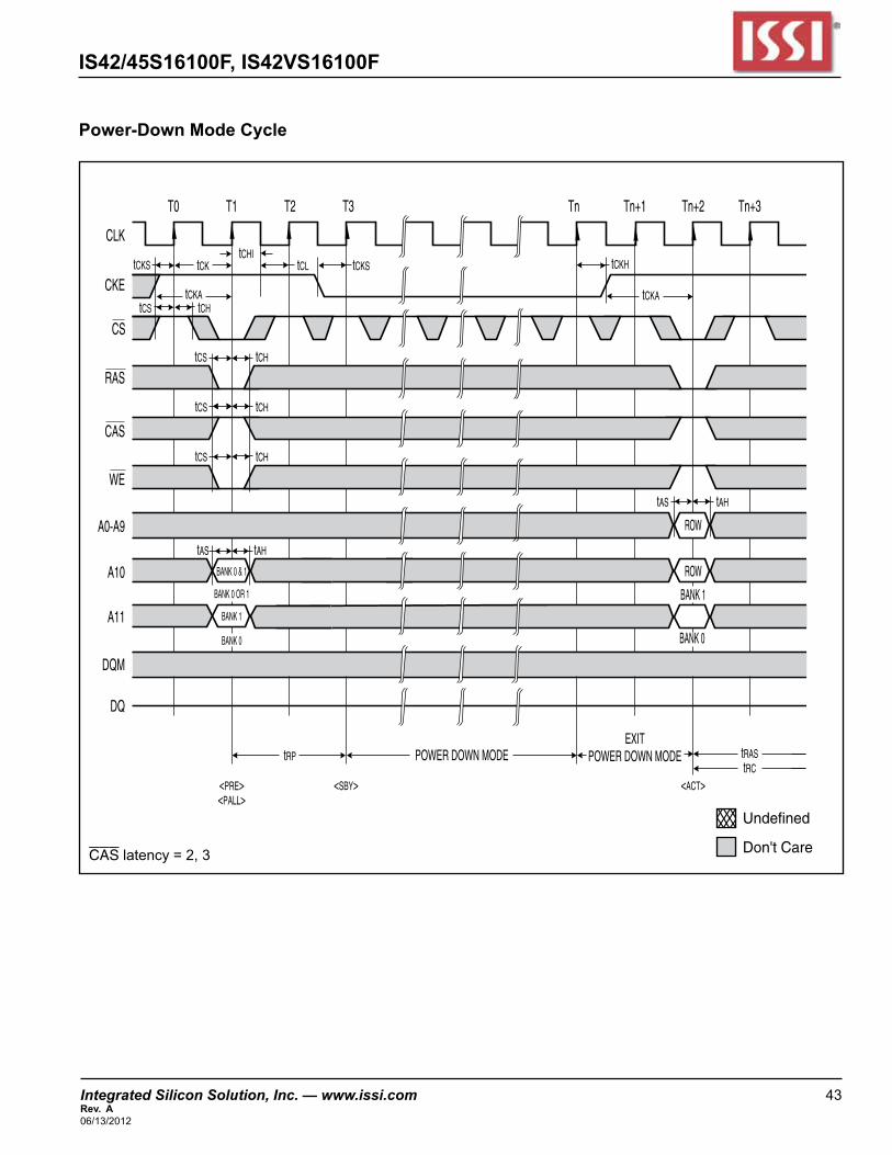
Power-Down Mode Cycle
CLK
CKE
CS
RAS
CAS
WE
A0-A9
A10
A11
DQM
DQ
T0 T1 T2 T3 Tn Tn+1 Tn+2 Tn+3
tCKtCKStCHI
tCL
tCHtCS
tCHtCS
tCHtCS
tCHtCS
tAHtAS
ROW
ROW
BANK 1
BANK 0
tCKS tCKH
tCKAtCKA
tAHtAS
tRP POWER DOWN MODEEXIT
POWER DOWN MODE tRAStRC
<ACT><SBY><PRE><PALL>
BANK 0 & 1
BANK 0 OR 1
BANK 1
BANK 0
CASlatency=2,3 Don't Care
Undefined
IS42/45S16100F, IS42VS16100F
44 Integrated Silicon Solution, Inc. — www.issi.com Rev. A
06/13/2012
CASlatency=2,3
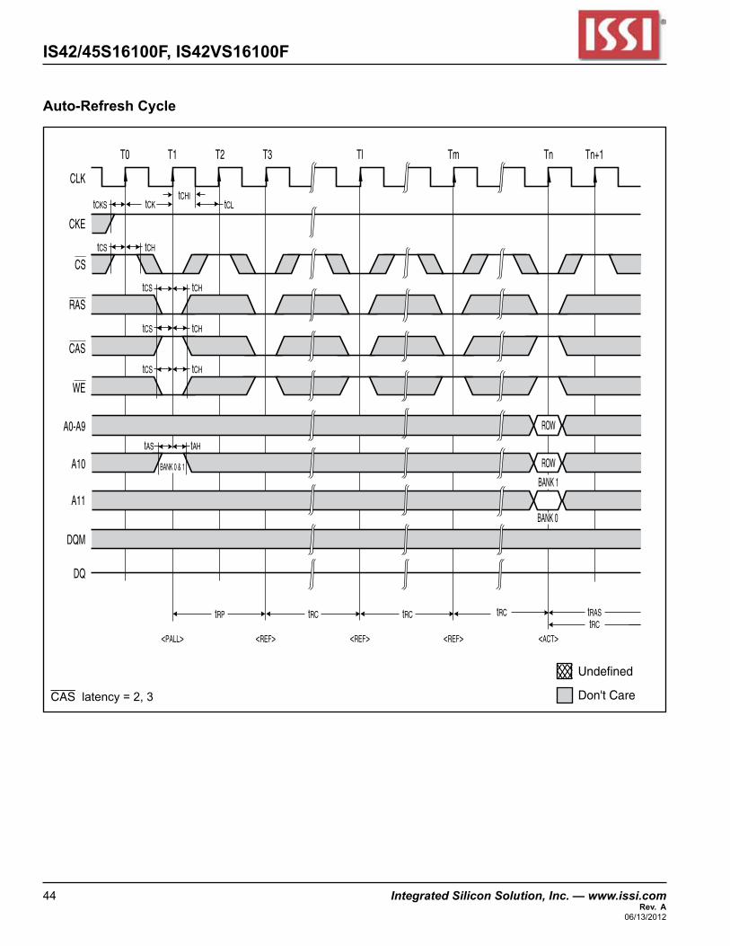
Auto-Refresh Cycle
CLK
CKE
CS
RAS
CAS
WE
A0-A9
A10
A11
DQM
DQ
T0 T1 T2 T3 Tl Tm Tn Tn+1
tCKtCHI
tCL
tCHtCS
tCHtCS
tCHtCS
tCHtCS
tAHtAS
BANK 0 & 1
ROW
ROW
BANK 1
BANK 0
tRP tRC tRC tRC tRAStRC
<ACT><REF> <REF><PALL> <REF>
tCKS
Don't Care
Undefined
Integrated Silicon Solution, Inc. — www.issi.com 45Rev. A06/13/2012
IS42/45S16100F, IS42VS16100F
CASlatency=2,3
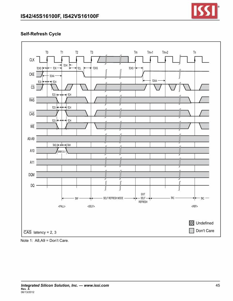
Self-Refresh Cycle
Don't Care
Undefined
CLK
CKE
CS
RAS
CAS
WE
A0-A9
A10
A11
DQM
DQ
T0 T1 T2 T3 Tm Tm+2Tm+1 Tn
tCKtCHI
tCL
tCHtCS
tCHtCS
tCHtCS
tCHtCS
tAHtAS
BANK 0 & 1
tCKStCKS
tCKA
tCKA
tRP SELF REFRESH MODEEXITSELF
REFRESHtRC tRC
<REF><PALL> <SELF>
tCKS
Note1:A8,A9=Don’tCare.
IS42/45S16100F, IS42VS16100F
46 Integrated Silicon Solution, Inc. — www.issi.com Rev. A
06/13/2012
CASlatency=2,burstlength=4 Don't Care
Undefined
CLK
CKE
CS
RAS
CAS
WE
A0-A9
A10
A11
DQM
DQ
T0 T1 T2 T3 T4 T5 T6 T7 T8 T9 T10
tCKtCHI
tCL
tCHtCS
tCHtCS
tCHtCS
tCHtCS
tAHtAS
BANK 1
BANK 0 AND 1
BANK 0 OR 1
NO PRE
tAHtAS
tCS
tAHtAS
tCKS
tCKA
BANK 0BANK 0
BANK 1 BANK 1
BANK 0
BANK 1
BANK 0
ROW ROW
ROW
COLUMN m
ROW
tQMD
tLZ
tRAS
tRC
<ACT> <READ> <ACT><PRE><PALL>
tRCD tCAC tRQL
tRP
tRCD
tAC tAC
tOH
tAC tAC
tOH
tCH
tOH
DOUT m DOUT m+1 DOUT m+2
tOH
tHZ
DOUT m+3
tRC
tRAS
(1)
Read Cycle
Note1:A8,A9=Don’tCare.
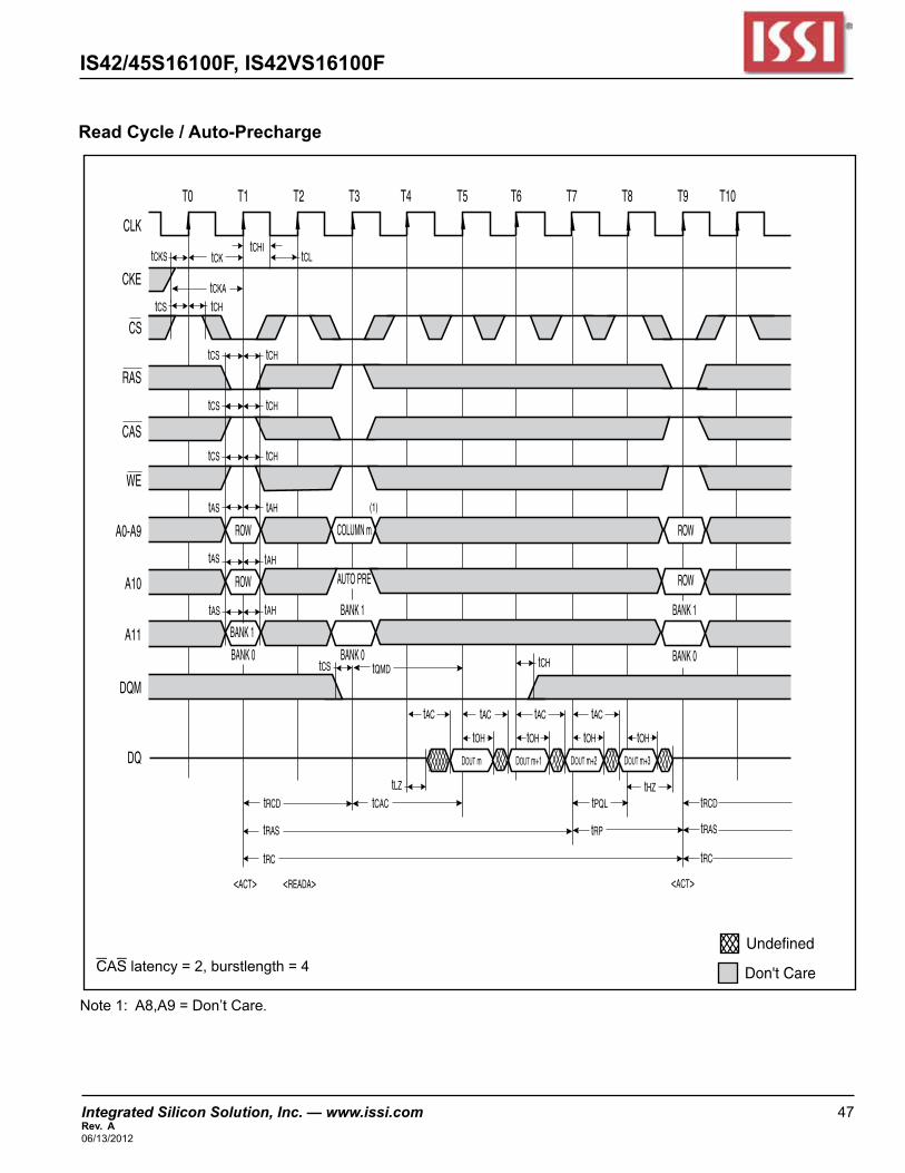
Integrated Silicon Solution, Inc. — www.issi.com 47Rev. A06/13/2012
IS42/45S16100F, IS42VS16100F
CASlatency=2,burstlength=4 Don't Care
Undefined
CLK
CKE
CS
RAS
CAS
WE
A0-A9
A10
A11
DQM
DQ
T0 T1 T2 T3 T4 T5 T6 T7 T8 T9 T10
tCKtCHI
tCL
tCHtCS
tCHtCS
tCHtCS
tCHtCS
tAHtAS
BANK 1
AUTO PRE
tAHtAS
tCS
tAHtAS
tCKS
tCKA
BANK 0BANK 0
BANK 1 BANK 1
BANK 0
ROW ROW
ROW
COLUMN m
ROW
tQMD
tLZ
tRAS
tRC
<ACT> <READA> <ACT>
tRCD tCAC tPQL
tRP
tRCD
tAC tAC
tOH
tAC tAC
tOH
tCH
tOH
DOUT m DOUT m+1 DOUT m+2
tOH
tHZ
DOUT m+3
tRC
tRAS
(1)
Read Cycle / Auto-Precharge
Note1:A8,A9=Don’tCare.
IS42/45S16100F, IS42VS16100F
48 Integrated Silicon Solution, Inc. — www.issi.com Rev. A
06/13/2012
Read Cycle / Full Page
CLK
CKE
CS
RAS
CAS
WE
A0-A9
A10
A11
DQM
DQ
T0 T1 T2 T3 T4 T5 T6 T260 T261 T262 T263
tCKtCHI
tCL
tCHtCS
tCHtCS
tCHtCS
tCHtCS
tAHtAS
NO PREtAHtAS
tCS
tAHtAS
tCKS
tCKA
BANK 0BANK 0
BANK 0 OR 1
BANK 0
ROW COLUMN
ROW
tQMD
tLZ
tRAS
tRC(BANK 0)
<ACT 0> <READ0> <BST> <PRE 0>
tRCD tCAC(BANK 0)
tRBD
tAC tAC
tOH
tAC tAC tAC
tOH
tCH
tOH
DOUT 0m DOUT 0m+1 DOUT 0m-1
tOH
tHZ
tOH
DOUT 0m DOUT 0m+1
tRP(BANK 0)
(1)
CASlatency=2,burstlength=fullpage Don't Care
Undefined
Note1:A8,A9=Don’tCare.
Integrated Silicon Solution, Inc. — www.issi.com 49Rev. A06/13/2012
IS42/45S16100F, IS42VS16100F
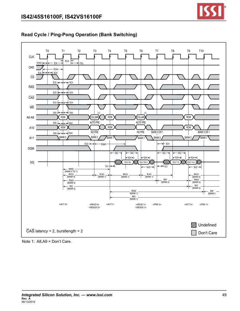
Read Cycle / Ping-Pong Operation (Bank Switching)
CLK
CKE
CS
RAS
CAS
WE
A0-A9
A10
A11
DQM
DQ
T0 T1 T2 T3 T4 T5 T6 T7 T8 T9 T10
tCKtCHI
tCL
tCHtCS
tCHtCS
tCHtCS
tCHtCS
tAHtAS
BANK 0 BANK 0 BANK 0 BANK 0 BANK 1BANK 1BANK 1
BANK 0 OR 1 BANK 0 OR 1NO PRE NO PRE
tCH
tAHtAS
tQMDtCS
tAC tAC tAC tAC
tRCD(BANK 0)
tRAS(BANK 0)
<ACT 0><ACT 0> <ACT1><READ 0><READA 0> <READA 1>
<READ 1> <PRE 0> <PRE 1>
tAHtAS
tCKS
tCKA
ROW ROW
ROW ROW
ROWCOLUMN COLUMN
AUTO PRE AUTO PRE
ROW
tLZ tLZ
tRCD(BANK 1)
tRAS(BANK 1)
tRC(BANK 1)
tCAC(BANK 1)
tCAC(BANK 1)
tRC(BANK 0)
tRP(BANK 0)
tRP(BANK1)
tRCD(BANK 0)
tRAS(BANK 0)
tRC(BANK 0)
tRRD(BANK 0 TO 1)
tOH tOH tOH tOH
tHZtHZ
DOUT 0m DOUT 0m+1 DOUT 1m DOUT 1m+1
(1)(1)
CASlatency=2,burstlength=2 Don't Care
Undefined
Note1:A8,A9=Don’tCare.
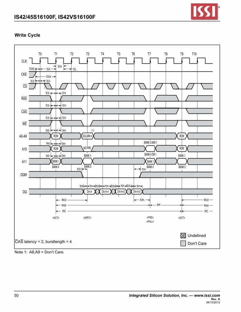
IS42/45S16100F, IS42VS16100F
50 Integrated Silicon Solution, Inc. — www.issi.com Rev. A
06/13/2012
Write Cycle
CLK
CKE
CS
RAS
CAS
WE
A0-A9
A10
A11
DQM
DQ
T0 T1 T2 T3 T4 T5 T7 T6 T8 T9 T10
tCKtCHI
tCL
tCHtCS
tCHtCS
tCHtCS
tCHtCS
tAHtAS
BANK 1
BANK 0
BANK 0 OR 1
BANK 0 AND 1
NO PRE
tCH
tAHtAS
tCS
tDS tDS tDS tDStDH
tRAS
tRC
<PRE><PALL>
<ACT><ACT> <WRIT>
tAHtAS
tCKS
tCKA
ROW ROW
ROW
COLUMN m
ROW
tRCD
tDH tDH tDH
tRP
tDPL tRCD
tRAS
tRC
DIN m DIN m+2DIN m+1 DIN m+3
BANK 1
BANK 0
BANK 1
BANK 0
BANK 1
BANK 0
(1)
CASlatency=2,burstlength=4 Don't Care
Undefined
Note1:A8,A9=Don’tCare.
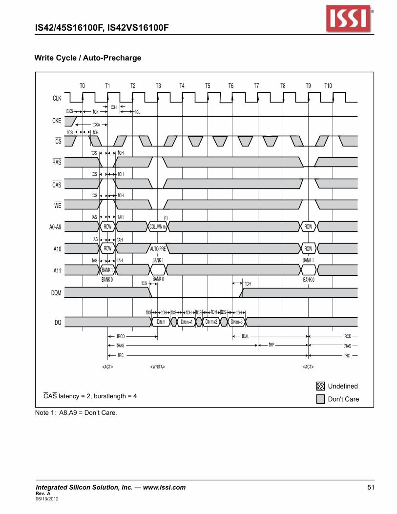
Integrated Silicon Solution, Inc. — www.issi.com 51Rev. A06/13/2012
IS42/45S16100F, IS42VS16100F
Write Cycle / Auto-Precharge
CLK
CKE
CS
RAS
CAS
WE
A0-A9
A10
A11
DQM
DQ
T0 T1 T2 T3 T4 T5 T7 T6 T8 T9 T10
tCKtCHI
tCL
tCHtCS
tCHtCS
tCHtCS
tCHtCS
tAHtAS
BANK 1
BANK 0
AUTO PRE
tCH
tAHtAS
tCS
tDS tDS tDS tDStDH
tRAS
tRC
<ACT><ACT> <WRITA>
tAHtAS
tCKS
tCKA
ROW ROW
ROW
COLUMN m
ROW
tRCD
tDH tDH tDH
tRP
tDAL tRCD
tRAS
tRC
DIN m DIN m+2DIN m+1 DIN m+3
BANK 1
BANK 0
BANK 1
BANK 0
(1)
CASlatency=2,burstlength=4 Don't Care
Undefined
Note1:A8,A9=Don’tCare.
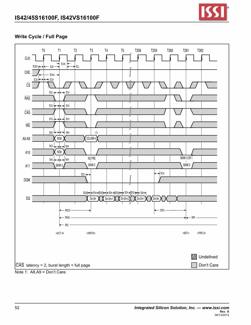
IS42/45S16100F, IS42VS16100F
52 Integrated Silicon Solution, Inc. — www.issi.com Rev. A
06/13/2012
Write Cycle / Full Page
CLK
CKE
CS
RAS
CAS
WE
A0-A9
A10
A11
DQM
DQ
T0 T1 T2 T3 T4 T5 T259T258 T260 T261 T262
tCKtCHI
tCL
tCHtCS
tCHtCS
tCHtCS
tCHtCS
tAHtAS
NO PREtAHtAS
tCS
tAHtAS
tCKS
tCKA
BANK 0BANK 0
BANK 0 OR 1
BANK 0
ROW COLUMN m
ROW
tRAS
tRC
<ACT 0> <WRIT0> <BST> <PRE 0>
tRCD
tCH
tDPL
tRP
tDS tDS tDS tDStDH tDH tDH tDH
DIN 0m DIN 0m+2DIN 0m+1 DIN 0m-1 DIN 0m
(1)
CAS latency=2,burstlength=fullpage Don't Care
Undefined
Note1:A8,A9=Don’tCare.
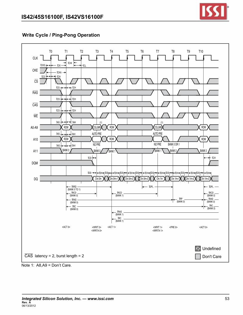
Integrated Silicon Solution, Inc. — www.issi.com 53Rev. A06/13/2012
IS42/45S16100F, IS42VS16100F
Write Cycle / Ping-Pong Operation
CLK
CKE
CS
RAS
CAS
WE
A0-A9
A10
A11
DQM
DQ
T0 T1 T2 T3 T4 T5 T6 T7 T8 T9 T10
tCKtCHI
tCL
tCHtCS
tCHtCS
tCHtCS
tCHtCS
tAHtAS
BANK 0 BANK 0 BANK 0 BANK 0BANK 1BANK 1
BANK 0 OR 1NO PRE NO PRE
tCH
tAHtAS
tCS
tDS tDS
tRCD(BANK 0)
tRAS(BANK 0)
<ACT 0> <ACT 1> <WRIT 0><WRITA 0> <WRITA 1>
<WRIT 1> <PRE 0> <ACT 0>
tAHtAS
tCKS
tCKA
ROW ROW
ROW
ROW
ROW
COLUMN COLUMN
AUTO PREAUTO PRE
ROW
tRCD(BANK 1)
tRAS(BANK 1)
tRC(BANK 1)
tRC(BANK 0)
tRCD(BANK 0)
tRP(BANK 0)
tRAS(BANK 0)
tRC(BANK 0)
tRRD(BANK 0 TO 1)
tDPL tDPL
tDH tDH tDS tDH tDH
DIN 0m
tDS tDS tDH tDS tDH tDH tDHtDS tDS
DIN 0m+1 DIN 0m+2 DIN 0m+3 DIN 1m DIN 1m+1 DIN 1m+2 DIN 1m+3
(1) (1)
Don't Care
Undefined
CAS latency=2,burstlength=2
Note1:A8,A9=Don’tCare.
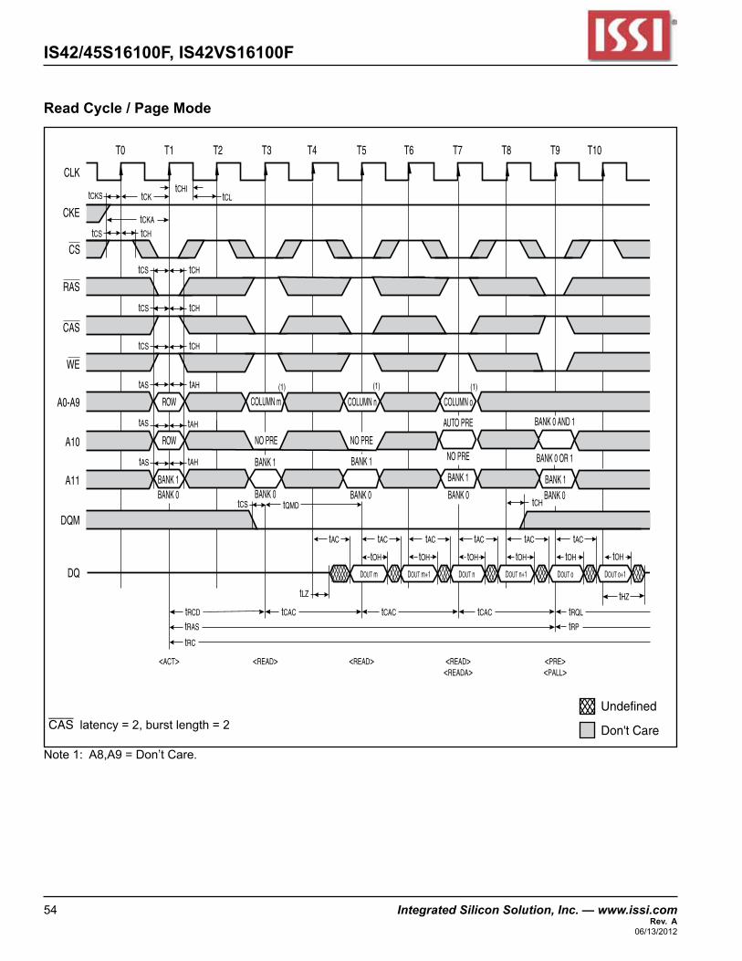
IS42/45S16100F, IS42VS16100F
54 Integrated Silicon Solution, Inc. — www.issi.com Rev. A
06/13/2012
Read Cycle / Page Mode
CLK
CKE
CS
RAS
CAS
WE
A0-A9
A10
A11
DQM
DQ
T0 T1 T2 T3 T4 T5 T6 T7 T8 T9 T10
tCKtCHI
tCL
tCHtCS
tCHtCS
tCHtCS
tCHtCS
tAHtAS
BANK 1 BANK 0 BANK 0 BANK 0 BANK 0
BANK 1
BANK 0 OR 1
BANK 0 AND 1
BANK 1
tCH
tAHtAS
tLZ
tCS
tRAS
tRC
<ACT> <READ><READA><READ><READ>
<PALL><PRE>
tAHtAS
tCKS
tCKA
ROW COLUMN m COLUMN n COLUMN o
NO PRE NO PRENO PRE
AUTO PRE
ROW
tRCD tCAC tCAC tCAC tRQL
tHZ
tRP
tQMD
BANK 1
BANK 0
BANK 1
tAC tAC
tOH
tAC tAC tAC tAC
tOH tOH tOH tOH tOH
DOUT m DOUT m+1 DOUT n DOUT n+1 DOUT o DOUT o+1
(1)(1)(1)
Don't Care
UndefinedCAS latency=2,burstlength=2
Note1:A8,A9=Don’tCare.
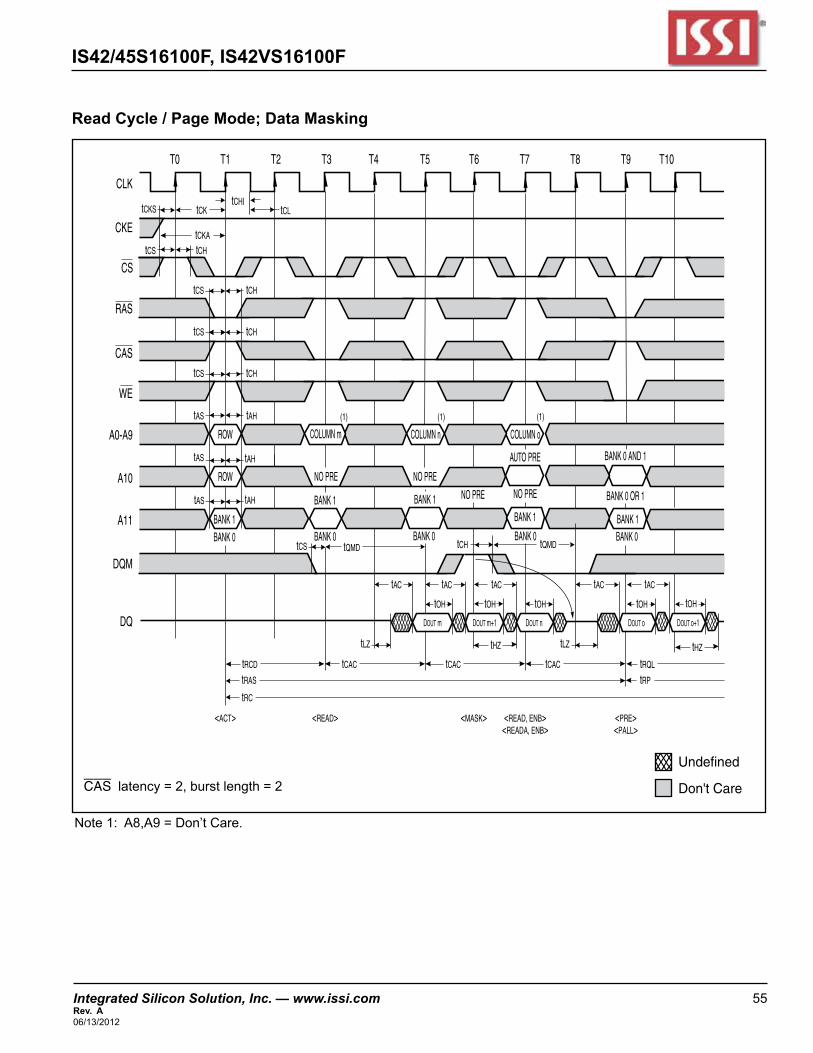
Integrated Silicon Solution, Inc. — www.issi.com 55Rev. A06/13/2012
IS42/45S16100F, IS42VS16100F
Read Cycle / Page Mode; Data Masking
CLK
CKE
CS
RAS
CAS
WE
A0-A9
A10
A11
DQM
DQ
T0 T1 T2 T3 T4 T5 T6 T7 T8 T9 T10
tCKtCHI
tCL
tCHtCS
tCHtCS
tCHtCS
tCHtCS
tAHtAS
BANK 1
BANK 0 BANK 0 BANK 0 BANK 0BANK 1
BANK 0 OR 1
BANK 0 AND 1
NO PRE BANK 1
tQMD
tAHtAS
tLZ
tCS
tRAS
tRC
<ACT> <READ><READA, ENB><READ, ENB><MASK>
<PALL><PRE>
tAHtAS
tCKS
tCKA
ROW COLUMN m COLUMN n COLUMN o
NO PRE NO PRENO PRE
AUTO PRE
ROW
tCH
tRCD tCAC tCAC tCAC tRQL
tHZtHZ
tRP
tQMD
BANK 1
BANK 0
BANK 1
tAC
tLZ
tAC
tOH
tAC tAC tAC
tOH tOH tOH tOH
DOUT m DOUT m+1 DOUT n DOUT o DOUT o+1
(1) (1) (1)
Don't Care
Undefined
CAS latency=2,burstlength=2
Note1:A8,A9=Don’tCare.
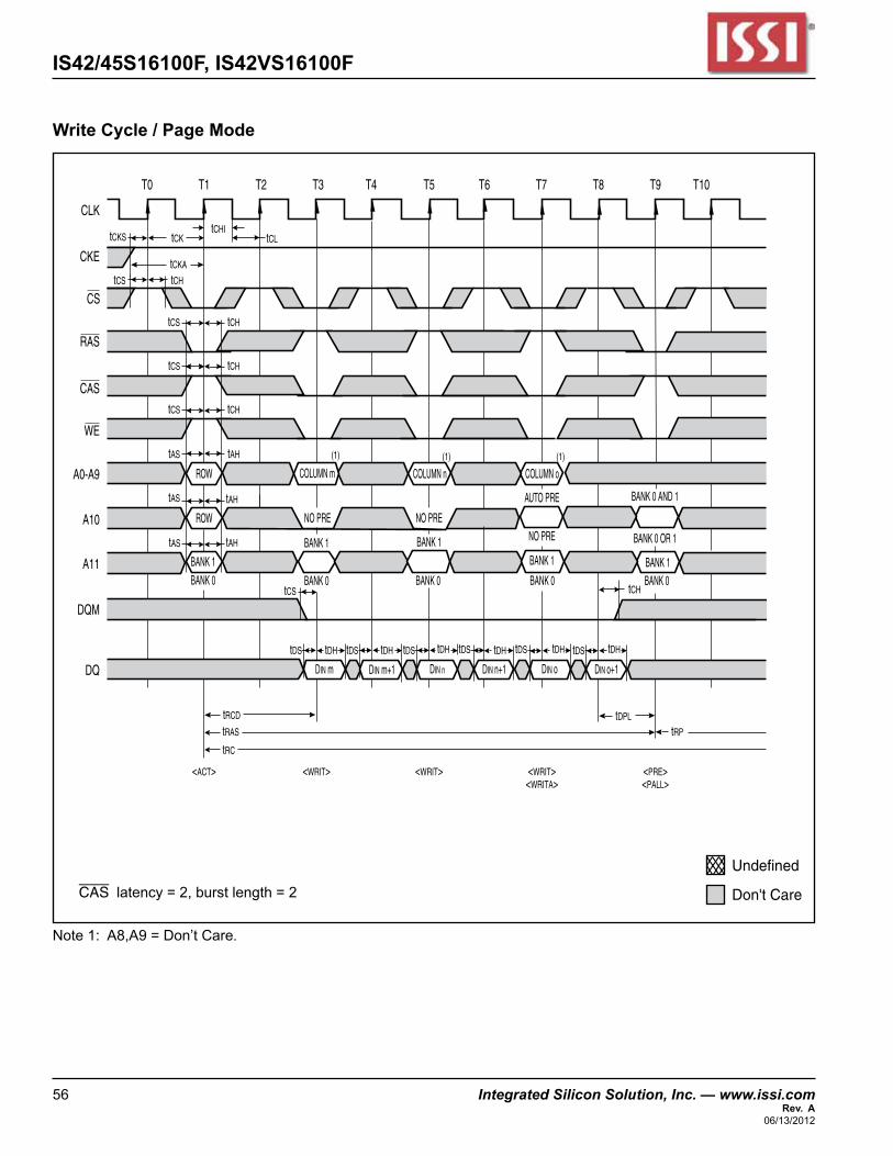
IS42/45S16100F, IS42VS16100F
56 Integrated Silicon Solution, Inc. — www.issi.com Rev. A
06/13/2012
Write Cycle / Page Mode
CLK
CKE
CS
RAS
CAS
WE
A0-A9
A10
A11
DQM
DQ
T0 T1 T2 T3 T4 T5 T6 T7 T8 T9 T10
tCKtCHI
tCL
tCHtCS
tCHtCS
tCHtCS
tCHtCS
tAHtAS
BANK 1
BANK 0 BANK 0 BANK 0 BANK 0BANK 1
BANK 0 OR 1
BANK 0 AND 1
BANK 1
tCH
tAHtAS
tCS
tRAS
tRC
<ACT> <WRIT><WRITA><WRIT><WRIT>
<PALL><PRE>
tAHtAS
tCKS
tCKA
ROW COLUMN m COLUMN n COLUMN o
NO PRE NO PRENO PRE
AUTO PRE
ROW
tRCD tDPL
tRP
BANK 1
BANK 0
BANK 1
tDS tDS tDS tDStDH tDStDH tDH tDH tDS tDHtDH
DIN m DIN nDIN m+1 DIN n+1 DIN o DIN o+1
(1) (1) (1)
Don't Care
Undefined
CAS latency=2,burstlength=2
Note1:A8,A9=Don’tCare.
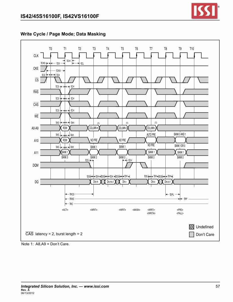
Integrated Silicon Solution, Inc. — www.issi.com 57Rev. A06/13/2012
IS42/45S16100F, IS42VS16100F
Write Cycle / Page Mode; Data Masking
CLK
CKE
CS
RAS
CAS
WE
A0-A9
A10
A11
DQM
DQ
T0 T1 T2 T3 T4 T5 T6 T7 T8 T9 T10
tCKtCHI
tCL
tCHtCS
tCHtCS
tCHtCS
tCHtCS
tAHtAS
BANK 1
BANK 0 BANK 0 BANK 0 BANK 0BANK 1
BANK 1OR 0
BANK 0 AND 1
BANK 1
tCH
tAHtAS
tCS
tRAS
tRC
<ACT> <WRIT> <WRIT><WRITA><WRIT><MASK>
<PALL><PRE>
tAHtAS
tCKS
tCKA
ROW COLUMN m COLUMN n COLUMN o
NO PRE NO PRENO PRE
AUTO PRE
ROW
tRCD tDPL
tRP
BANK 1
BANK 0
BANK 1
tDS tDS tDStDH tDStDH tDH tDH tDS tDH
DIN m DIN nDIN m+1 DIN o DIN o+1
(1)(1)(1)
Don't Care
Undefined
CAS latency=2,burstlength=2
Note1:A8,A9=Don’tCare.
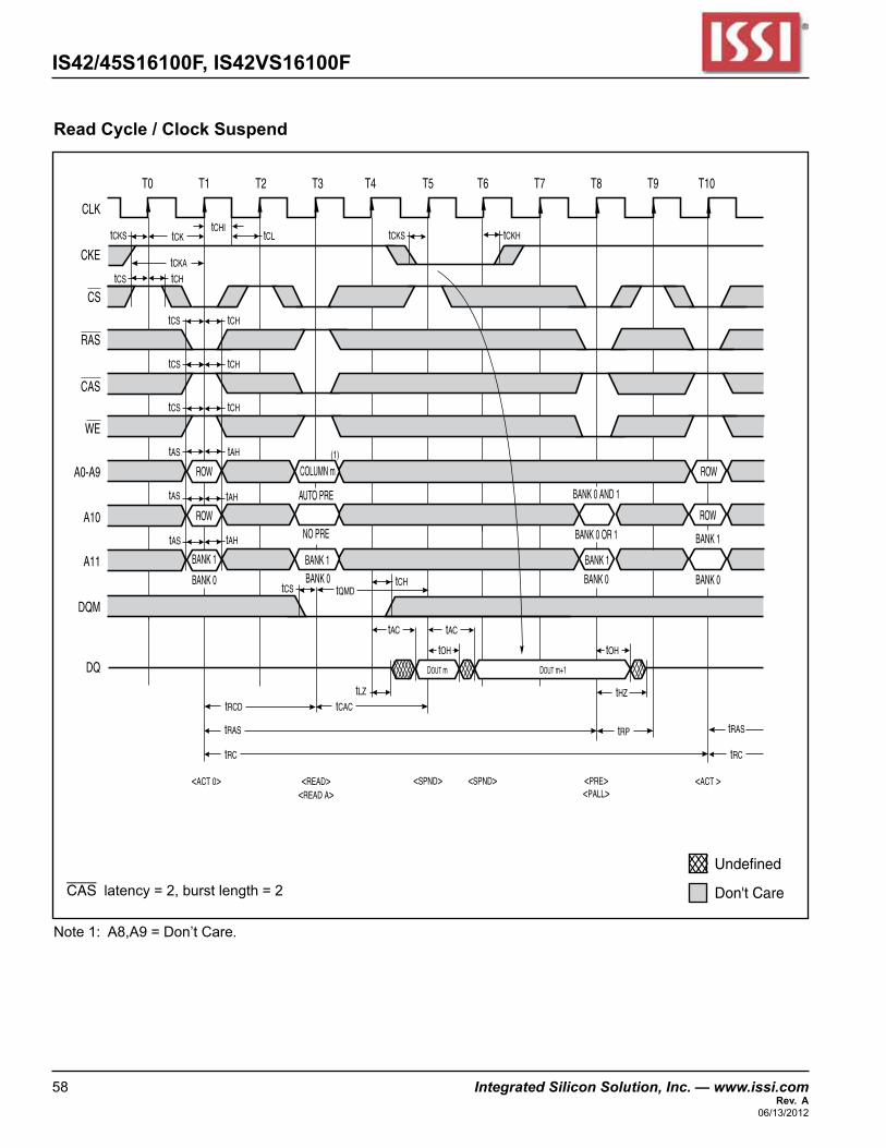
IS42/45S16100F, IS42VS16100F
58 Integrated Silicon Solution, Inc. — www.issi.com Rev. A
06/13/2012
Read Cycle / Clock Suspend
CLK
CKE
CS
RAS
CAS
WE
A0-A9
A10
A11
DQM
DQ
T0 T1 T2 T3 T4 T5 T6 T7 T8 T9 T10
tCKtCHI
tCL
tCHtCS
tCHtCS
tCHtCS
tCHtCS
tAHtAS
NO PRE
AUTO PRE
tAHtAS
tCS
tCKH
tAHtAS
tCKS
tCKA
tCKS
BANK 1BANK 0
BANK 1
BANK 1
BANK 0 BANK 0
BANK 1
BANK 0
BANK 0 AND 1
BANK 0 OR 1
ROW ROW
ROW
COLUMN m
ROW
tQMD
tLZ
tRAS
tRC tRC
<ACT 0> <ACT ><READ><READ A>
<SPND> <SPND> <PRE><PALL>
tRCD tCAC
tAC tAC
tOH tOH
tCH
DOUT m DOUT m+1
tHZ
tRP tRAS
(1)
Don't Care
Undefined
CAS latency=2,burstlength=2
Note1:A8,A9=Don’tCare.
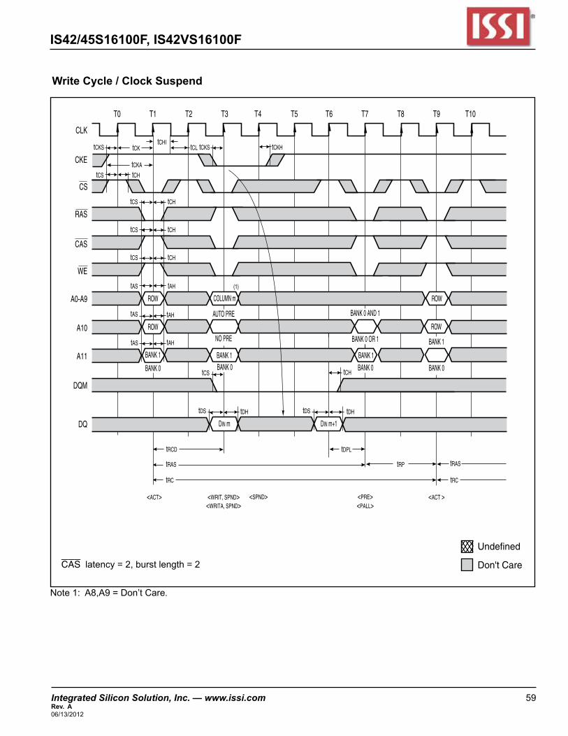
Integrated Silicon Solution, Inc. — www.issi.com 59Rev. A06/13/2012
IS42/45S16100F, IS42VS16100F
Write Cycle / Clock Suspend
CLK
CKE
CS
RAS
CAS
WE
A0-A9
A10
A11
DQM
DQ
T0 T1 T2 T3 T4 T5 T6 T7 T8 T9 T10
tCKtCHI
tCL
tCHtCS
tCHtCS
tCHtCS
tCHtCS
tAHtAS
NO PRE
AUTO PRE
tAHtAS
tCS
tCKH
tAHtAS
tCKS
tCKA
tCKS
BANK 1BANK 0
BANK 1
BANK 1
BANK 0 BANK 0
BANK 1
BANK 0
BANK 0 AND 1
BANK 0 OR 1
ROW ROW
ROW
COLUMN m
ROW
tDS
tRAS
tRC tRC
<ACT> <ACT ><WRIT, SPND><WRITA, SPND>
<SPND> <PRE><PALL>
tRCD
tCH
tDH tDH tDS
tDPL
tRP tRAS
DIN m DIN m+1
(1)
Don't Care
Undefined
CAS latency=2,burstlength=2
Note1:A8,A9=Don’tCare.
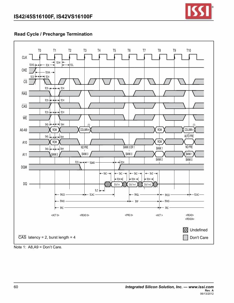
IS42/45S16100F, IS42VS16100F
60 Integrated Silicon Solution, Inc. — www.issi.com Rev. A
06/13/2012
Read Cycle / Precharge Termination
CLK
CKE
CS
RAS
CAS
WE
A0-A9
A10
A11
DQM
DQ
T0 T1 T2 T3 T4 T5 T6 T7 T8 T9 T10
tCKtCHI
tCL
tCHtCS
tCHtCS
tCHtCS
tCHtCS
tAHtAS
NO PRE
AUTO PRE
NO PREtAHtAS
tCS
tAHtAS
tCKS
tCKA
BANK 0 BANK 0
BANK 1
BANK 0 BANK 0
BANK 0
BANK 0 OR 1
ROW ROW
ROW
COLUMN m COLUMN n
ROW
tQMD
tLZ
tRAS
tRC tRC
<ACT 0> <ACT ><READ 0> <PRE 0> <READ><READA>
tRCD tCAC tRQL
tRP
tRCD
tAC tAC
tOH
tAC tHZ
tOH tOH
tCH
DOUT m DOUT m+2
tRAS
tCAC
BANK 1
DOUT m+1
(1) (1)
Don't Care
Undefined
CAS latency=2,burstlength=4
Note1:A8,A9=Don’tCare.
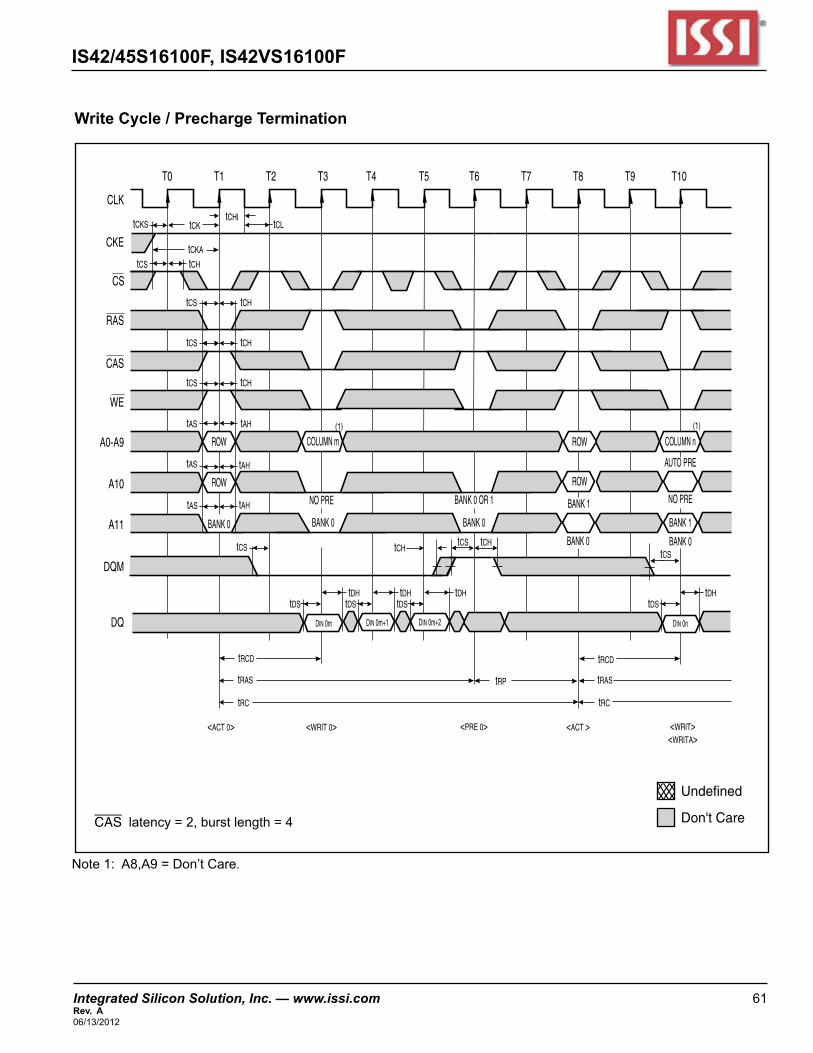
Integrated Silicon Solution, Inc. — www.issi.com 61Rev. A06/13/2012
IS42/45S16100F, IS42VS16100F
Write Cycle / Precharge Termination
CLK
CKE
CS
RAS
CAS
WE
A0-A9
A10
A11
DQM
DQ
T0 T1 T2 T3 T4 T5 T6 T7 T8 T9 T10
tCKtCHI
tCL
tCHtCS
tCHtCS
tCHtCS
tCHtCS
tAHtAS
NO PRE
AUTO PRE
NO PREtAHtAS
tAHtAS
tCKS
tCKA
BANK 0 BANK 0
BANK 1
BANK 0 BANK 0
BANK 0
BANK 0 OR 1
ROW ROW
ROW
COLUMN m COLUMN n
ROW
tRAS
tRC tRC
<ACT 0> <ACT ><WRIT 0> <PRE 0> <WRIT><WRITA>
tRCD
tRP
tRCD
tRAS
BANK 1
DIN 0m DIN 0nDIN 0m+1 DIN 0m+2
tDStDStDStDStDHtDHtDHtDH
tCStCH tCStCS
tCH
(1) (1)
Don't Care
Undefined
CAS latency=2,burstlength=4
Note1:A8,A9=Don’tCare.
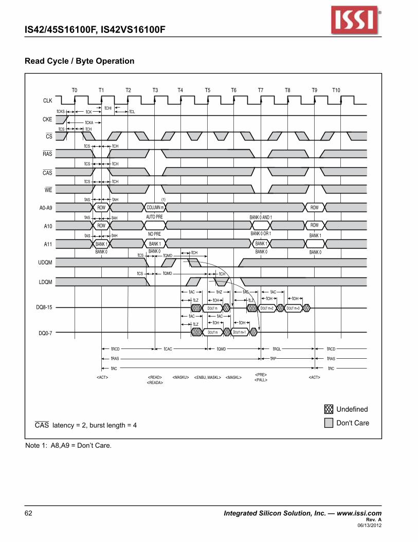
IS42/45S16100F, IS42VS16100F
62 Integrated Silicon Solution, Inc. — www.issi.com Rev. A
06/13/2012
Read Cycle / Byte Operation
CLK
CKE
CS
RAS
CAS
WE
A0-A9
A10
A11
LDQM
UDQM
DQ8-15
DQ0-7
T0 T1 T2 T3 T4 T5 T6 T7 T8 T9 T10
tCKtCHI
tCL
tCHtCS
tCHtCS
tCHtCS
tCHtCS
tAHtAS
BANK 1 BANK 1
BANK 0 AND 1
BANK 0 OR 1NO PRE
AUTO PRE
tCH
tAHtAS
tCS
tCS tCH
tAHtAS
tCKS
tCKA
BANK 0BANK 0
BANK 1
BANK 1
BANK 0 BANK 0
ROW COLUMN m
ROW
tQMD
tQMD
tRAS
tRC
<ACT> <ACT><READ><READA>
<MASKU> <MASKL><ENBU, MASKL> <PALL><PRE>
tRCD tCAC tQMD tRQL tRCD
tRAS
tRC
tRP
tAC tHZ
tOH
tAC tAC
tLZ
tLZ
tLZ
DOUT m
DOUT m
DOUT m+2
DOUT m+1
DOUT m+3
tOH
tOH
tOH
tACtAC
tOH
ROW
ROW
(1)
Don't Care
Undefined
CAS latency=2,burstlength=4
Note1:A8,A9=Don’tCare.
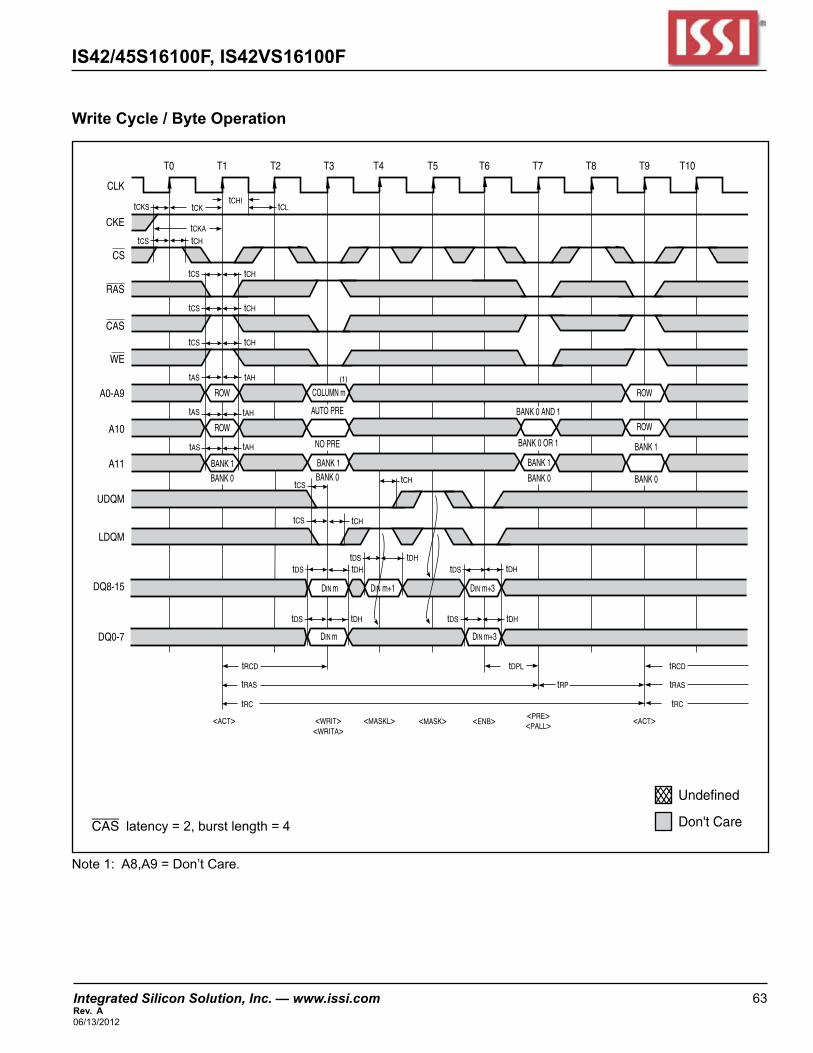
Integrated Silicon Solution, Inc. — www.issi.com 63Rev. A06/13/2012
IS42/45S16100F, IS42VS16100F
Write Cycle / Byte Operation
CLK
CKE
CS
RAS
CAS
WE
A0-A9
A10
A11
LDQM
UDQM
DQ8-15
DQ0-7
T0 T1 T2 T3 T4 T5 T6 T7 T8 T9 T10
tCKtCHI
tCL
tCHtCS
tCHtCS
tCHtCS
tCHtCS
tAHtAS
BANK 1 BANK 1
BANK 0 AND 1
BANK 0 OR 1NO PRE
AUTO PRE
tCH
tAHtAS
tCS
tCS tCH
tAHtAS
tCKS
tCKA
BANK 0BANK 0
BANK 1
BANK 1
BANK 0 BANK 0
ROW COLUMN m
ROW
tRAS
tRC
<ACT> <ACT><WRIT><WRITA>
<MASK><MASKL> <ENB> <PALL><PRE>
tRCD tDPL tRCD
tRAS
tRC
tRP
ROW
ROW
tDH tDS tDS
tDH tDS
tDH tDS
DIN m
DIN m DIN m+3
tDH
tDH tDS
DIN m+1 DIN m+3
(1)
Don't Care
Undefined
CAS latency=2,burstlength=4
Note1:A8,A9=Don’tCare.
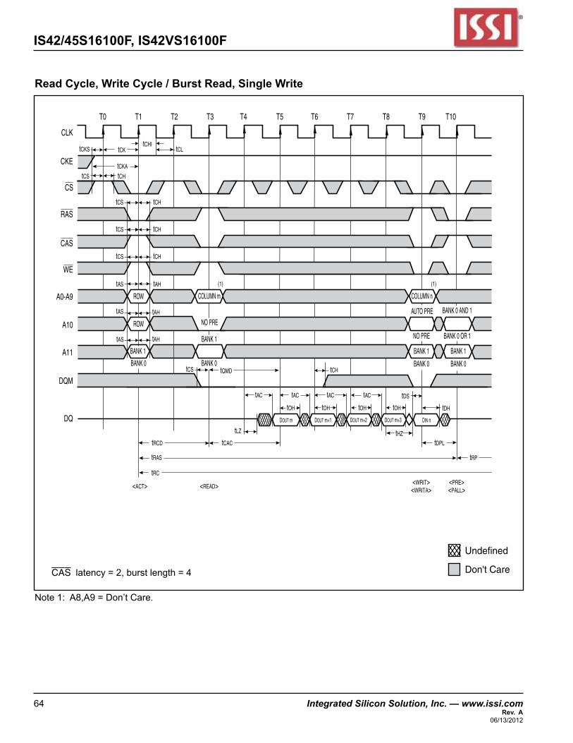
IS42/45S16100F, IS42VS16100F
64 Integrated Silicon Solution, Inc. — www.issi.com Rev. A
06/13/2012
Read Cycle, Write Cycle / Burst Read, Single Write
COLUMN n
CLK
CKE
CS
RAS
CAS
WE
A0-A9
A10
A11
DQM
DQ
T0 T1 T2 T3 T4 T5 T6 T7 T8 T9 T10
tCKtCHI
tCL
tCHtCS
tCHtCS
tCHtCS
tCHtCS
tAHtAS
BANK 1
BANK 0 AND 1
BANK 0 OR 1
NO PRE
NO PRE
AUTO PRE
tCH
tAHtAS
tCS
tAHtAS
tCKS
tCKA
BANK 0BANK 0
BANK 1
BANK 1
BANK 0
BANK 1
BANK 0
ROW COLUMN m
ROW
tQMD
tHZtLZ
tRAS
tRC
<ACT> <READ> <WRITA><WRIT>
<PALL><PRE>
tRCD tCAC tDPL
tRP
tAC tAC
tOH
tAC tAC
tOH tDH
tDS
tOH
DOUT m DOUT m+1 DOUT m+2
tOH
DOUT m+3 DIN n
(1) (1)
Don't Care
Undefined
CAS latency=2,burstlength=4
Note1:A8,A9=Don’tCare.
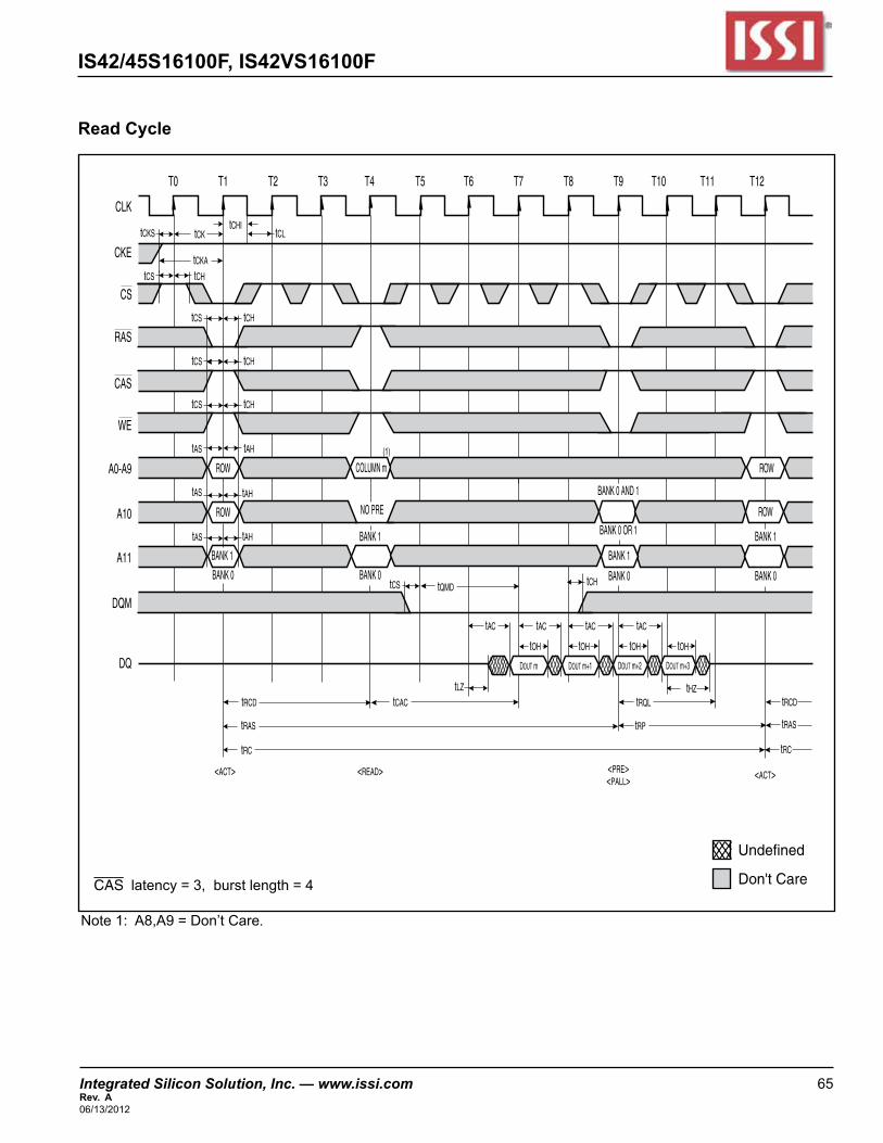
Integrated Silicon Solution, Inc. — www.issi.com 65Rev. A06/13/2012
IS42/45S16100F, IS42VS16100F
Read Cycle
CLK
CKE
CS
RAS
CAS
WE
A0-A9
A10
A11
DQM
DQ
T0 T1 T2 T3 T4 T5 T6 T7 T8 T9 T10 T11 T12
tCKtCHI
tCL
tCHtCS
tCHtCS
tCHtCS
tCHtCS
tAHtAS
BANK 1
BANK 0 AND 1
BANK 0 OR 1
NO PRE
tAHtAS
tCS
tAHtAS
tCKS
tCKA
BANK 0BANK 0
BANK 1 BANK 1
BANK 0
BANK 1
BANK 0
ROW ROW
ROW
COLUMN m
ROW
tQMD
tLZ
tRAS
tRC
<ACT> <READ> <ACT><PRE><PALL>
tRCD tCAC tRQL
tRP
tRCD
tAC tAC
tOH
tAC tAC
tOH
tCH
tOH
DOUT m DOUT m+1 DOUT m+2
tOH
tHZ
DOUT m+3
tRC
tRAS
(1)
Don't Care
Undefined
CAS latency=3,burstlength=4
Note1:A8,A9=Don’tCare.
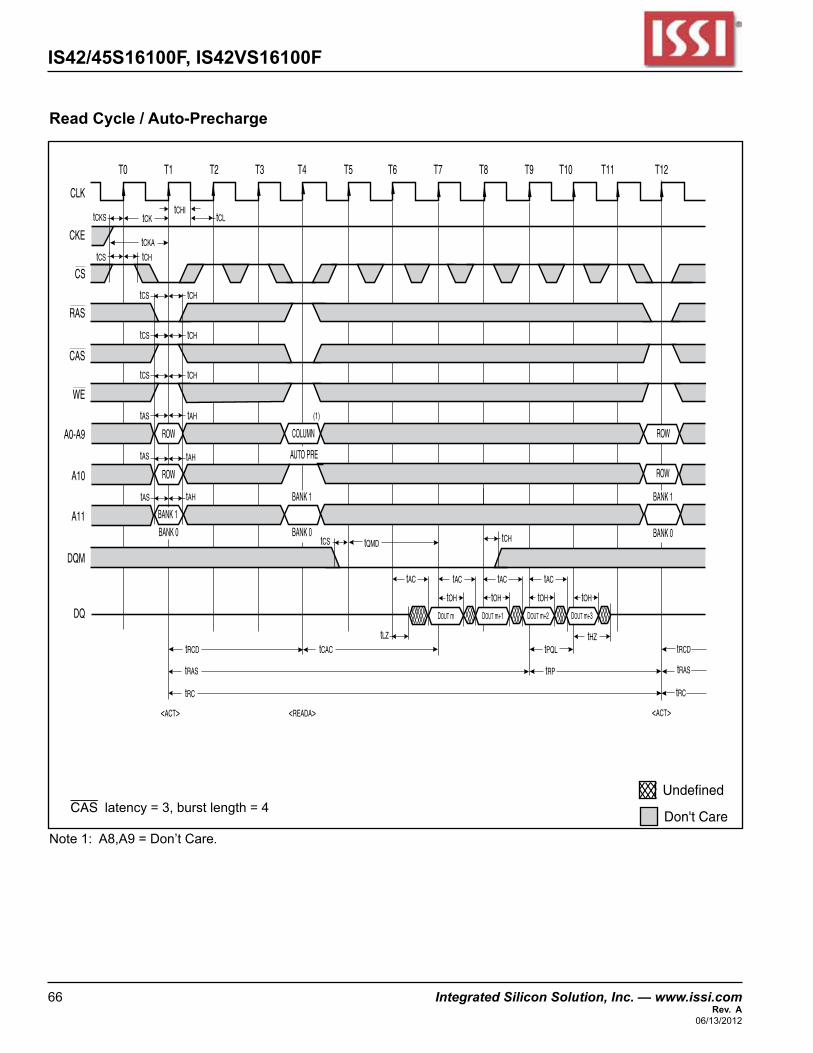
IS42/45S16100F, IS42VS16100F
66 Integrated Silicon Solution, Inc. — www.issi.com Rev. A
06/13/2012
Read Cycle / Auto-Precharge
CLK
CKE
CS
RAS
CAS
WE
A0-A9
A10
A11
DQM
DQ
T0 T1 T2 T3 T4 T5 T6 T7 T8 T9 T10 T11 T12
tCKtCHI
tCL
tCHtCS
tCHtCS
tCHtCS
tCHtCS
tAHtAS
BANK 1
AUTO PRE
tAHtAS
tCS
tAHtAS
tCKS
tCKA
BANK 0BANK 0
BANK 1 BANK 1
BANK 0
ROW
ROW
ROWCOLUMN
ROW
tQMD
tLZ
tRAS
tRC
<ACT> <READA> <ACT>
tRCD tCAC tPQL
tRP
tRCD
tAC tAC
tOH
tAC tAC
tOH
tCH
tOH
DOUT m DOUT m+1 DOUT m+2
tOH
tHZ
DOUT m+3
tRC
tRAS
(1)
CAS latency=3,burstlength=4Don't Care
Undefined
Note1:A8,A9=Don’tCare.
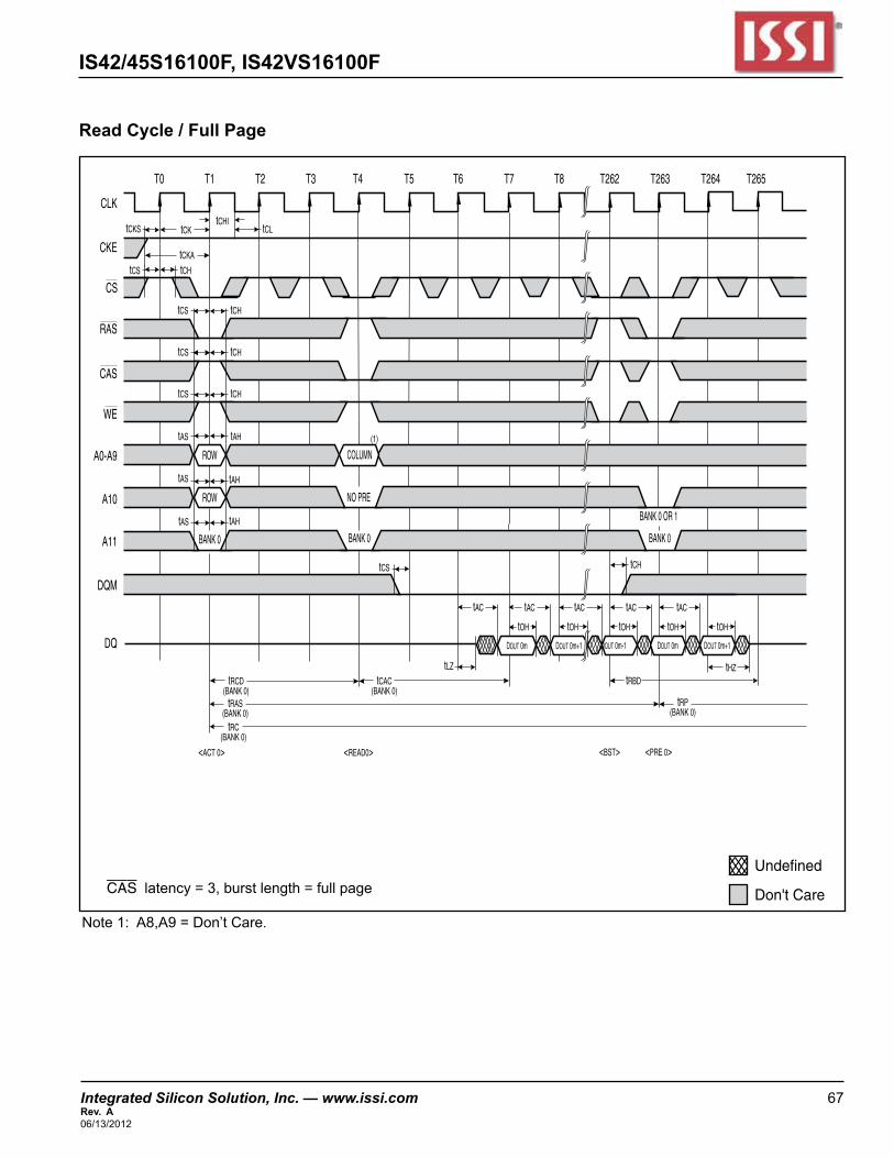
Integrated Silicon Solution, Inc. — www.issi.com 67Rev. A06/13/2012
IS42/45S16100F, IS42VS16100F
Read Cycle / Full Page
CLK
CKE
CS
RAS
CAS
WE
A0-A9
A10
A11
DQM
DQ
T0 T1 T2 T3 T4 T5 T6 T7 T8 T262 T263 T264 T265
tCKtCHI
tCL
tCHtCS
tCHtCS
tCHtCS
tCHtCS
tAHtAS
NO PRE
tAHtAS
tCS
tAHtAS
tCKS
tCKA
BANK 0BANK 0
BANK 0 OR 1
BANK 0
ROW COLUMN
ROW
tLZ
tRAS(BANK 0)
tRC(BANK 0)
<ACT 0> <READ0> <BST> <PRE 0>
tRCD(BANK 0)
tCAC(BANK 0)
tRBD
tAC tAC
tOH
tAC tAC tAC
tOH
tCH
tOH
DOUT 0m DOUT 0m+1 DOUT 0m-1
tOH
tHZ
tOH
DOUT 0m DOUT 0m+1
tRP(BANK 0)
(1)
CAS latency=3,burstlength=fullpage Don't Care
Undefined
Note1:A8,A9=Don’tCare.
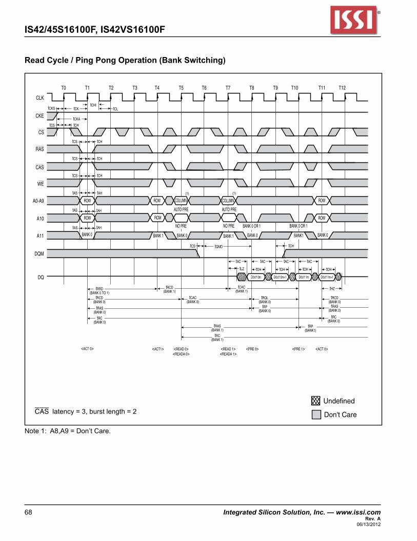
IS42/45S16100F, IS42VS16100F
68 Integrated Silicon Solution, Inc. — www.issi.com Rev. A
06/13/2012
Read Cycle / Ping Pong Operation (Bank Switching)
CLK
CKE
CS
RAS
CAS
WE
A0-A9
A10
A11
DQM
DQ
T0 T1 T2 T3 T4 T5 T6 T7 T8 T9 T10 T11 T12
tCKtCHI
tCL
tCHtCS
tCHtCS
tCHtCS
tCHtCS
tAHtAS
BANK 0 BANK 1 BANK 0 BANK1 BANK 0BANK 1BANK 0
BANK 0 OR 1 BANK 0 OR 1NO PRE NO PRE
tCH
tAHtAS
tQMDtCS
tAC tAC tAC tAC
tRCD(BANK 0)
tRAS(BANK 0)
<ACT 0><ACT 0> <ACT1> <READ 0><READA 0> <READA 1>
<READ 1> <PRE 0> <PRE 1>
tAHtAS
tCKS
tCKA
ROW ROW
ROW ROW
ROWCOLUMN COLUMN
AUTO PRE AUTO PRE
ROW
tLZ
tRAS(BANK 1)
tRC(BANK 1)
tRCD(BANK 1)
tCAC(BANK 1)
tCAC(BANK 0)
tRC(BANK 0)
tRQL(BANK 0)
tRP(BANK 0)
tRCD(BANK 0)
tRAS(BANK 0)
tRP(BANK1)
tRC(BANK 0)
tRRD(BANK 0 TO 1)
tOH tOH tOH tOH
tHZ
DOUT 0m DOUT 0m+1 DOUT 1m DOUT 1m+1
(1) (1)
CAS latency=3,burstlength=2 Don't Care
Undefined
Note1:A8,A9=Don’tCare.
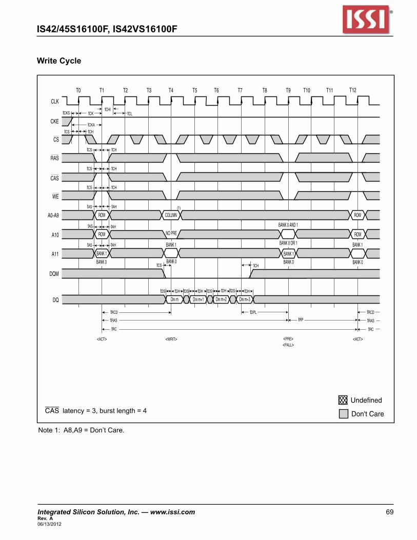
Integrated Silicon Solution, Inc. — www.issi.com 69Rev. A06/13/2012
IS42/45S16100F, IS42VS16100F
Write Cycle
CLK
CKE
CS
RAS
CAS
WE
A0-A9
A10
A11
DQM
DQ
T0 T1 T2 T3 T4 T5 T7 T6 T8 T9 T10 T11
tCKtCHI
tCL
tCHtCS
tCHtCS
tCHtCS
tCHtCS
tAHtAS
BANK 1
BANK 0
BANK 0 OR 1
BANK 0 AND 1
NO PRE
tCH
tAHtAS
tCS
tDS tDS tDS tDStDH
tRAS
tRC
<PRE><PALL>
<ACT><ACT> <WRIT>
tAHtAS
tCKS
tCKA
ROW ROW
ROW
COLUMN
ROW
tRCD
tDH tDH tDH
tRP
tDPL tRCD
tRAS
tRC
DIN m DIN m+2DIN m+1 DIN m+3
BANK 1
BANK 0
BANK 1
BANK 0
BANK 1
BANK 0
T12
(1)
CAS latency=3,burstlength=4 Don't Care
Undefined
Note1:A8,A9=Don’tCare.
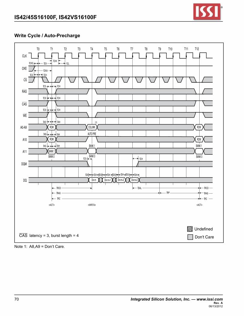
IS42/45S16100F, IS42VS16100F
70 Integrated Silicon Solution, Inc. — www.issi.com Rev. A
06/13/2012
Write Cycle / Auto-Precharge
CLK
CKE
CS
RAS
CAS
WE
A0-A9
A10
A11
DQM
DQ
T0 T1 T2 T3 T4 T5 T7 T6 T8 T9 T10
tCKtCHI
tCL
tCHtCS
tCHtCS
tCHtCS
tCHtCS
tAHtAS
BANK 1
BANK 0
AUTO PRE
tCH
tAHtAS
tCS
tDS tDS tDS tDStDH
tRAS
tRC
<ACT><ACT> <WRITA>
tAHtAS
tCKS
tCKA
ROW ROW
ROW
COLUMN
ROW
tRCD
tDH tDH tDH
tRP
tDAL tRCD
tRAS
tRC
DIN m DIN m+2DIN m+1 DIN m+3
BANK 1
BANK 0
BANK 1
BANK 0
T11 T12
(1)
CAS latency=3,burstlength=4 Don't Care
Undefined
Note1:A8,A9=Don’tCare.
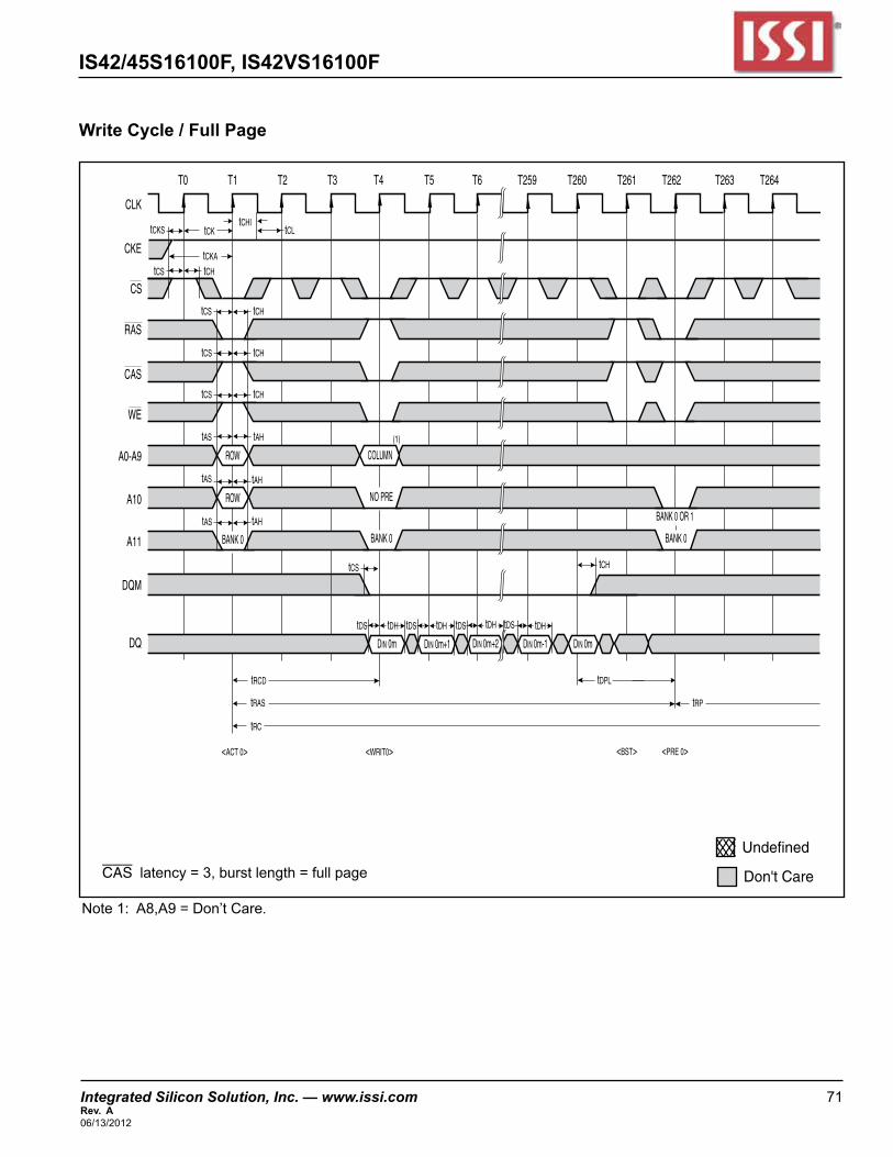
Integrated Silicon Solution, Inc. — www.issi.com 71Rev. A06/13/2012
IS42/45S16100F, IS42VS16100F
Write Cycle / Full Page
CLK
CKE
CS
RAS
CAS
WE
A0-A9
A10
A11
DQM
DQ
T0 T1 T2 T3 T4 T5 T259T6 T260 T261 T262 T263 T264
tCKtCHI
tCL
tCHtCS
tCHtCS
tCHtCS
tCHtCS
tAHtAS
NO PRE
tAHtAS
tCS
tAHtAS
tCKS
tCKA
BANK 0BANK 0
BANK 0 OR 1
BANK 0
ROW COLUMN
ROW
tRAS
tRC
<ACT 0> <WRIT0> <BST> <PRE 0>
tRCD
tCH
tDPL
tRP
tDS tDS tDS tDStDH tDH tDH tDH
DIN 0m DIN 0m+2DIN 0m+1 DIN 0m-1 DIN 0m
(1)
CAS latency=3,burstlength=fullpage Don't Care
Undefined
Note1:A8,A9=Don’tCare.
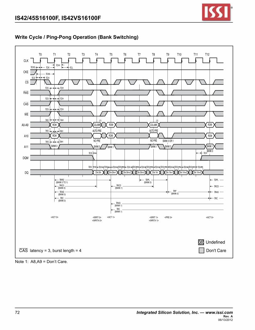
IS42/45S16100F, IS42VS16100F
72 Integrated Silicon Solution, Inc. — www.issi.com Rev. A
06/13/2012
Write Cycle / Ping-Pong Operation (Bank Switching)
CLK
CKE
CS
RAS
CAS
WE
A0-A9
A10
A11
DQM
DQ
T0 T1 T2 T3 T4 T5 T6 T7 T8 T9 T10
tCKtCHI
tCL
tCHtCS
tCHtCS
tCHtCS
tCHtCS
tAHtAS
BANK 0 BANK 0 BANK 0BANK 1BANK 1
BANK 0 OR 1NO PRE NO PRE
tCH
tAHtAS
tCS
tDS tDS
tRCD(BANK 0)
tRAS(BANK 0)
<ACT 0> <ACT 1> <WRIT 0><WRITA 0> <WRITA 1>
<WRIT 1> <PRE 0> <ACT 0>
tAHtAS
tCKS
tCKA
ROW ROW
ROW
ROW
ROW
COLUMN COLUMN
AUTO PREAUTO PRE
ROW
tRCD(BANK 1)
tRAS(BANK 1)
tRC(BANK 1)
tRC(BANK 0)
tRCD
tRP(BANK 0)
tRAS
tRC
tRRD(BANK 0 TO 1)
tDPL(BANK 0)
tDPL
tDH tDH tDS tDH tDH
DIN 0m
tDS tDS tDH tDS tDH tDH tDHtDS tDS
DIN 0m+1 DIN 0m+2 DIN 0m+3 DIN 1m DIN 1m+1 DIN 1m+2 DIN 1m+3
T11 T12
BANK 0
BANK 1
(1) (1)
CAS latency=3,burstlength=4 Don't Care
Undefined
Note1:A8,A9=Don’tCare.
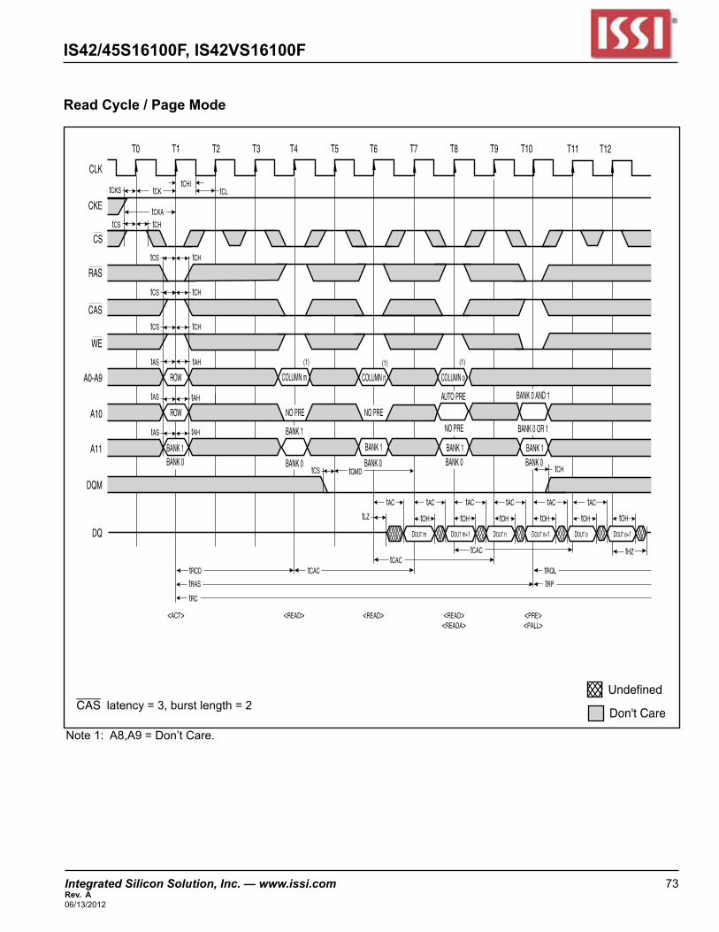
Integrated Silicon Solution, Inc. — www.issi.com 73Rev. A06/13/2012
IS42/45S16100F, IS42VS16100F
Read Cycle / Page Mode
CLK
CKE
CS
RAS
CAS
WE
A0-A9
A10
A11
DQM
DQ
T0 T1 T2 T3 T4 T5 T6 T7 T8 T9 T10
tCKtCHI
tCL
tCHtCS
tCHtCS
tCHtCS
tCHtCS
tAHtAS
BANK 1 BANK 0 BANK 0 BANK 0 BANK 0
BANK 1
BANK 0 OR 1
BANK 0 AND 1
BANK 1
tCH
tAHtAS
tLZ
tCS
tRAS
tRC
<ACT> <READ><READA><READ><READ>
<PALL><PRE>
tAHtAS
tCKS
tCKA
ROW COLUMN m COLUMN n COLUMN o
NO PRE NO PRE
NO PRE
AUTO PRE
ROW
tRCD tCACtCAC
tCAC
tRQL
tHZ
tRP
tQMD
BANK 1
BANK 0 BANK 1
tAC tAC
tOH
tAC tAC tAC tAC
tOH tOH tOH tOH tOH
DOUT m DOUT m+1 DOUT n DOUT n+1 DOUT o DOUT o+1
T11 T12
(1) (1)(1)
CAS latency=3,burstlength=2Don't Care
Undefined
Note1:A8,A9=Don’tCare.
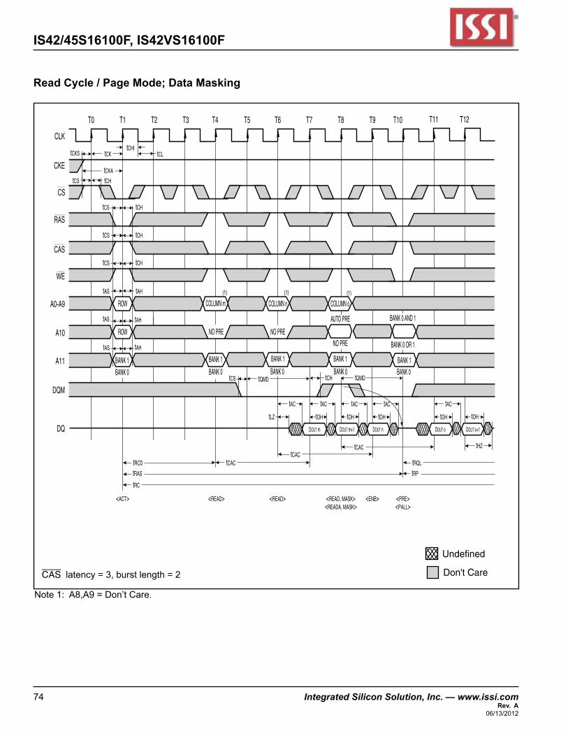
IS42/45S16100F, IS42VS16100F
74 Integrated Silicon Solution, Inc. — www.issi.com Rev. A
06/13/2012
Read Cycle / Page Mode; Data Masking
CAS latency=3,burstlength=2
CLK
CKE
CS
RAS
CAS
WE
A0-A9
A10
A11
DQM
DQ
T0 T1 T2 T3 T4 T5 T6 T7 T8 T9 T10
tCKtCHI
tCL
tCHtCS
tCHtCS
tCHtCS
tCHtCS
tAHtAS
BANK 1
BANK 0 BANK 0 BANK 0 BANK 0BANK 1
BANK 0 OR 1
BANK 0 AND 1
BANK 1
tQMD
tAHtAS
tLZ
tCS
tRAS
tRC
<ACT> <READ> <READ> <ENB><READA, MASK><READ, MASK>
<PALL><PRE>
tAHtAS
tCKS
tCKA
ROW COLUMN m COLUMN n COLUMN o
NO PRE NO PRENO PRE
AUTO PRE
ROW
tCH
tRCD tCACtCAC
tCAC
tRQL
tHZ
tRP
tQMD
BANK 1
BANK 0
BANK 1
tAC tAC
tOH
tAC tAC tAC
tOH tOH tOH tOH
DOUT m DOUT m+1 DOUT n DOUT o DOUT o+1
T11 T12
(1) (1) (1)
Don't Care
Undefined
Note1:A8,A9=Don’tCare.
Integrated Silicon Solution, Inc. — www.issi.com 75Rev. A06/13/2012
IS42/45S16100F, IS42VS16100F
Write Cycle / Page Mode
CAS latency=3,burstlength=2
CLK
CKE
CS
RAS
CAS
WE
A0-A9
A10
A11
DQM
DQ
T0 T1 T2 T3 T4 T5 T6 T7 T8 T9 T10
tCKtCHI
tCL
tCHtCS
tCHtCS
tCHtCS
tCHtCS
tAHtAS
BANK 0
BANK 0 BANK 0 BANK 0BANK 1
BANK 0 OR 1
BANK 0 AND 1
BANK 1
tCH
tAHtAS
tCS
tRAS
tRC
<ACT> <WRIT><WRITA><WRIT><WRIT> <MASK>
<PALL><PRE>
tAHtAS
tCKS
tCKA
ROW COLUMN m COLUMN n COLUMN o
NO PRE NO PRENO PRE
AUTO PRE
ROW
tRCD tDPL
tRP
BANK 1
BANK 0
BANK 1
tDS tDS tDStDH tDStDH tDH tDH tDS tDH
DIN m DIN nDIN m+1 DIN o DIN o+1
T11 T12
(1) (1) (1)
Don't Care
Undefined
Note1:A8,A9=Don’tCare.
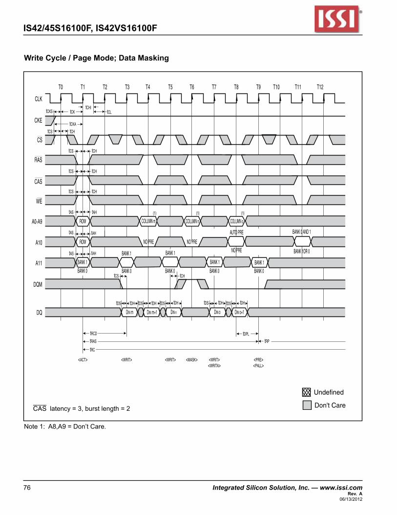
IS42/45S16100F, IS42VS16100F
76 Integrated Silicon Solution, Inc. — www.issi.com Rev. A
06/13/2012
Write Cycle / Page Mode; Data Masking
CAS latency=3,burstlength=2
CLK
CKE
CS
RAS
CAS
WE
A0-A9
A10
A11
DQM
DQ
T0 T1 T2 T3 T4 T5 T6 T7 T8 T9 T10 T11 T12
tCKtCHI
tCL
tCHtCS
tCHtCS
tCHtCS
tCHtCS
tAHtAS
BANK 1
BANK 0 BANK 0 BANK 0 BANK 0BANK 1
BANK 1OR 0
BANK 0 AND 1
BANK 1
tCH
tAHtAS
tCS
tRAS
tRC
<ACT> <WRIT> <WRIT><WRITA><WRIT><MASK>
<PALL><PRE>
tAHtAS
tCKS
tCKA
ROW COLUMN m COLUMN n COLUMN o
NO PRE NO PRENO PRE
AUTO PRE
ROW
tRCD tDPL
tRP
BANK 1
BANK 0
BANK 1
tDS tDS tDStDH tDStDH tDH tDH tDS tDH
DIN m DIN nDIN m+1 DIN o DIN o+1
(1) (1) (1)
Don't Care
Undefined
Note1:A8,A9=Don’tCare.
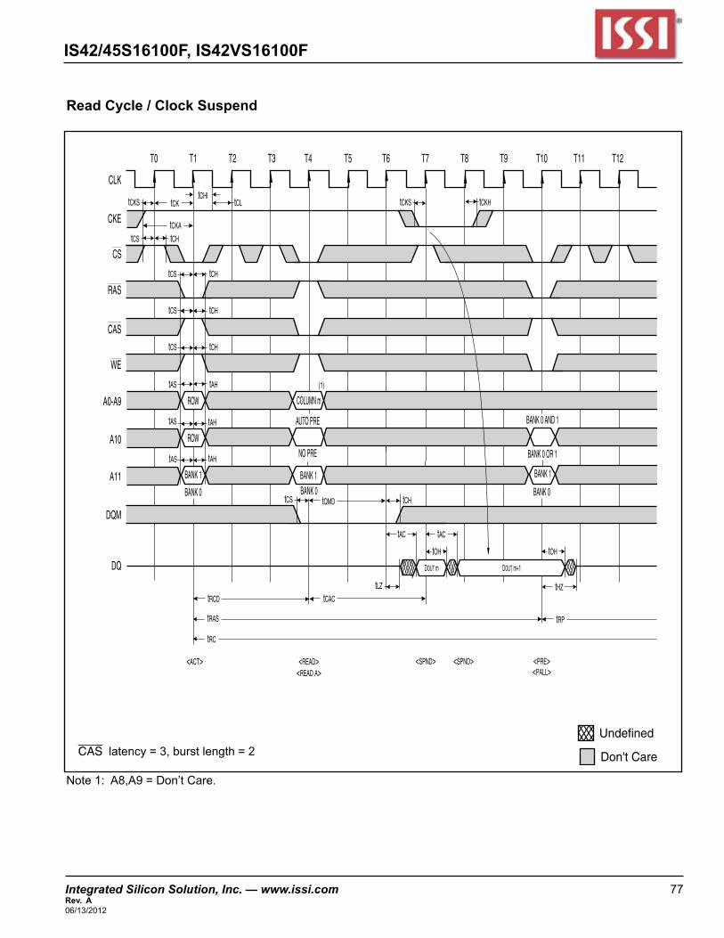
Integrated Silicon Solution, Inc. — www.issi.com 77Rev. A06/13/2012
IS42/45S16100F, IS42VS16100F
Read Cycle / Clock Suspend
CAS latency=3,burstlength=2
CLK
CKE
CS
RAS
CAS
WE
A0-A9
A10
A11
DQM
DQ
T0 T1 T2 T3 T4 T5 T6 T7 T8 T9 T10 T11
tCKtCHI
tCL
tCHtCS
tCHtCS
tCHtCS
tCHtCS
tAHtAS
NO PRE
AUTO PRE
tAHtAS
tCS
tCKH
tAHtAS
tCKS
tCKA
tCKS
BANK 1BANK 0 BANK 0
BANK 1
BANK 0
BANK 0 AND 1
BANK 0 OR 1
ROW COLUMN m
ROW
tQMD
tLZ
tRAS
tRC
<ACT> <READ><READ A>
<SPND> <SPND> <PRE><PALL>
tRCD tCAC
tAC tAC
tOH tOH
tCH
DOUT m DOUT m+1
tHZ
tRP
T12
BANK 1
(1)
Don't Care
Undefined
Note1:A8,A9=Don’tCare.
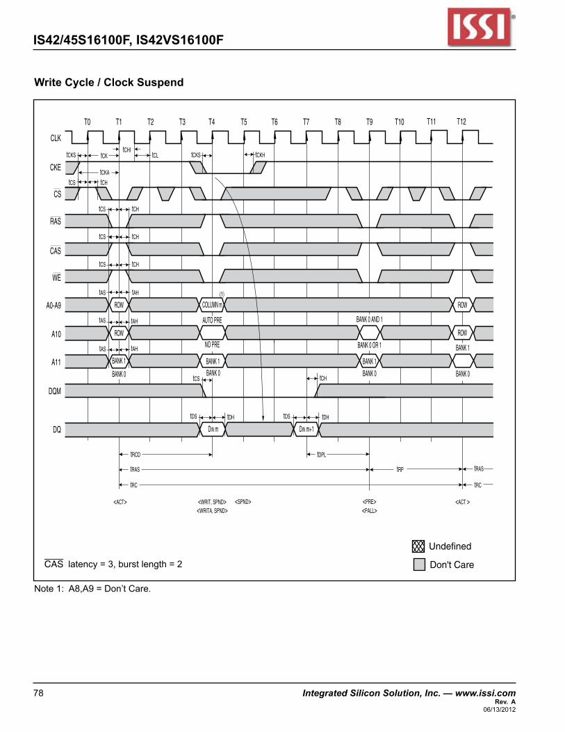
IS42/45S16100F, IS42VS16100F
78 Integrated Silicon Solution, Inc. — www.issi.com Rev. A
06/13/2012
Write Cycle / Clock Suspend
CAS latency=3,burstlength=2
CLK
CKE
CS
RAS
CAS
WE
A0-A9
A10
A11
DQM
DQ
T0 T1 T2 T3 T4 T5 T6 T7 T8 T9 T10
tCKtCHI
tCL
tCHtCS
tCHtCS
tCHtCS
tCHtCS
tAHtAS
NO PRE
AUTO PRE
tAHtAS
tCS
tCKH
tAHtAS
tCKS
tCKA
tCKS
BANK 1BANK 0
BANK 1
BANK 1
BANK 0 BANK 0
BANK 1
BANK 0
BANK 0 AND 1
BANK 0 OR 1
ROW ROW
ROW
COLUMN m
ROW
tDS
tRAS
tRC tRC
<ACT> <ACT ><WRIT, SPND><WRITA, SPND>
<SPND> <PRE><PALL>
tRCD
tCH
tDH tDH tDS
tDPL
tRP tRAS
DIN m DIN m+1
T11 T12
(1)
Don't Care
Undefined
Note1:A8,A9=Don’tCare.
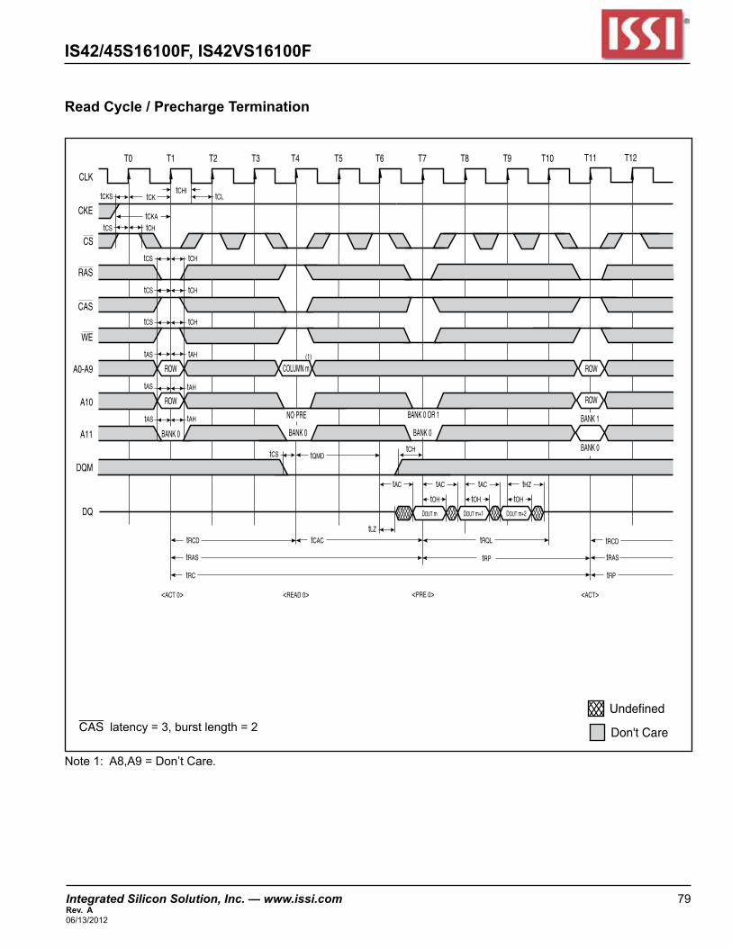
Integrated Silicon Solution, Inc. — www.issi.com 79Rev. A06/13/2012
IS42/45S16100F, IS42VS16100F
Read Cycle / Precharge Termination
CAS latency=3,burstlength=2
CLK
CKE
CS
RAS
CAS
WE
A0-A9
A10
A11
DQM
DQ
T0 T1 T2 T3 T4 T5 T6 T7 T8 T9 T10
tCKtCHI
tCL
tCHtCS
tCHtCS
tCHtCS
tCHtCS
tAHtAS
NO PREtAHtAS
tCS
tAHtAS
tCKS
tCKA
BANK 0
BANK 0
BANK 0
ROW ROW
ROW
COLUMN m
ROW
tQMD
tLZ
tRAS
tRC tRP
<ACT 0> <ACT><READ 0> <PRE 0>
tRCD tCAC tRQL
tRP
tRCD
tAC tAC
tOH
tAC tHZ
tOH tOH
tCH
DOUT m DOUT m+2
tRAS
BANK 1
DOUT m+1
T11 T12
BANK 0
BANK 0 OR 1
(1)
Don't Care
Undefined
Note1:A8,A9=Don’tCare.
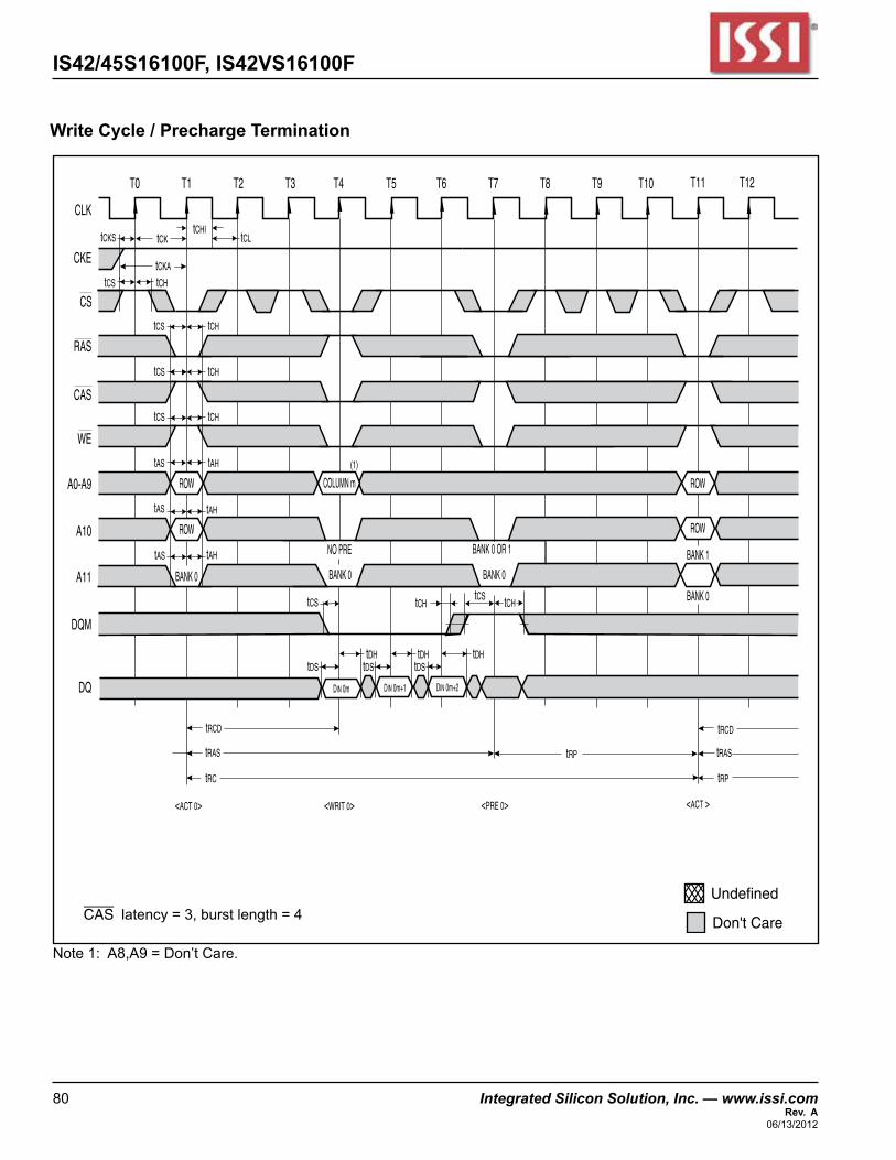
IS42/45S16100F, IS42VS16100F
80 Integrated Silicon Solution, Inc. — www.issi.com Rev. A
06/13/2012
Write Cycle / Precharge Termination
CAS latency=3,burstlength=4
CLK
CKE
CS
RAS
CAS
WE
A0-A9
A10
A11
DQM
DQ
T0 T1 T2 T3 T4 T5 T6 T7 T8 T9 T10
tCKtCHI
tCL
tCHtCS
tCHtCS
tCHtCS
tCHtCS
tAHtAS
NO PREtAHtAS
tAHtAS
tCKS
tCKA
BANK 0
BANK 0
BANK 0
ROW ROW
ROW
COLUMN m
ROW
tRC tRP
<ACT 0> <ACT ><WRIT 0> <PRE 0>
tRCD
tRP
tRCD
tRAS
BANK 1
DIN 0m DIN 0m+1 DIN 0m+2
tDStDStDStDHtDHtDH
T11 T12
tCH tCHtCS tCS
BANK 0
BANK 0 OR 1
tRAS
(1)
Don't Care
Undefined
Note1:A8,A9=Don’tCare.
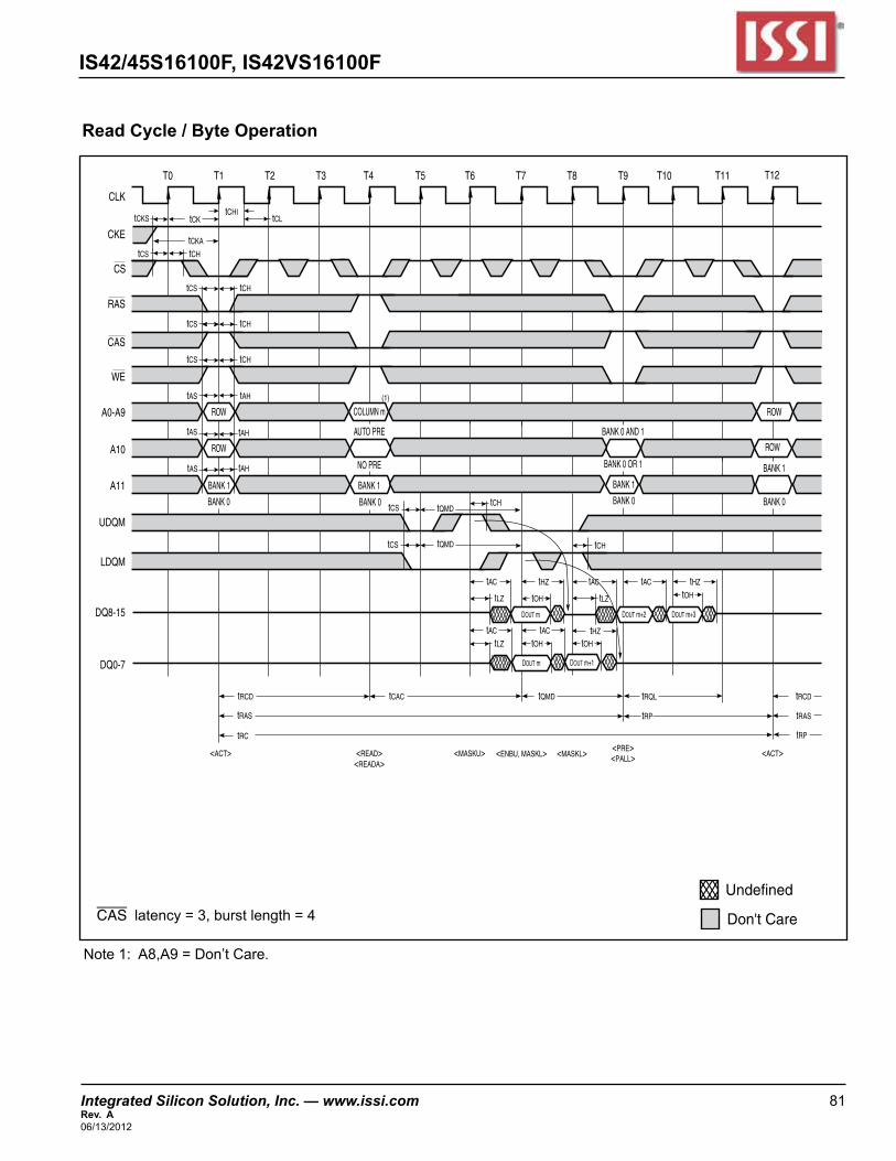
Integrated Silicon Solution, Inc. — www.issi.com 81Rev. A06/13/2012
IS42/45S16100F, IS42VS16100F
Read Cycle / Byte Operation
CAS latency=3,burstlength=4
CLK
CKE
CS
RAS
CAS
WE
A0-A9
A10
A11
LDQM
UDQM
DQ8-15
DQ0-7
T0 T1 T2 T3 T4 T5 T6 T7 T8 T9 T10 T11
tCKtCHI
tCL
tCHtCS
tCHtCS
tCHtCS
tCHtCS
tAHtAS
BANK 1 BANK 1
BANK 0 AND 1
BANK 0 OR 1NO PRE
AUTO PRE
tCH
tAHtAS
tCS
tCS tCH
tAHtAS
tCKS
tCKA
BANK 0BANK 0
BANK 1
BANK 1
BANK 0 BANK 0
ROW COLUMN m
ROW
tQMD
tQMD
tRAS
tRC
<ACT> <ACT><READ><READA>
<MASKU> <MASKL><ENBU, MASKL> <PALL><PRE>
tRCD tCAC tQMD tRQL tRCD
tRAS
tRP
tRP
tAC tHZ
tOH
tHZ
tHZ
tAC tAC
tLZ
tLZ
tLZ
DOUT m
DOUT m
DOUT m+2
DOUT m+1
DOUT m+3
tOH
tOH
tACtAC
tOH
ROW
ROW
T12
(1)
Don't Care
Undefined
Note1:A8,A9=Don’tCare.
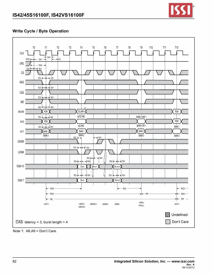
IS42/45S16100F, IS42VS16100F
82 Integrated Silicon Solution, Inc. — www.issi.com Rev. A
06/13/2012
Write Cycle / Byte Operation
CAS latency=3,burstlength=4
CLK
CKE
CS
RAS
CAS
WE
A0-A9
A10
A11
LDQM
UDQM
DQ8-15
DQ0-7
T0 T1 T2 T3 T4 T5 T6 T7 T8 T9 T10
tCKtCHI
tCL
tCHtCS
tCHtCS
tCHtCS
tCHtCS
tAHtAS
BANK 1 BANK 1
BANK 0 AND 1
BANK 0 OR 1NO PRE
AUTO PRE
tCH
tAHtAS
tCS
tCS tCH
tAHtAS
tCKS
tCKA
BANK 0BANK 0
BANK 1
BANK 1
BANK 0 BANK 0
ROW COLUMN m
ROW
tRAS
tRC
<ACT> <ACT><WRIT><WRITA>
<MASK><MASKL> <ENB> <PALL><PRE>
tRCD tDPL tRCD
tRAStRP
tRP
ROW
ROW
tDH tDS tDS
tDH tDS
tDH tDS
DIN m
DIN m DIN m+3
tDH
tDH tDS
DIN m+1 DIN m+3
T12T11
(1)
Don't Care
Undefined
Note1:A8,A9=Don’tCare.
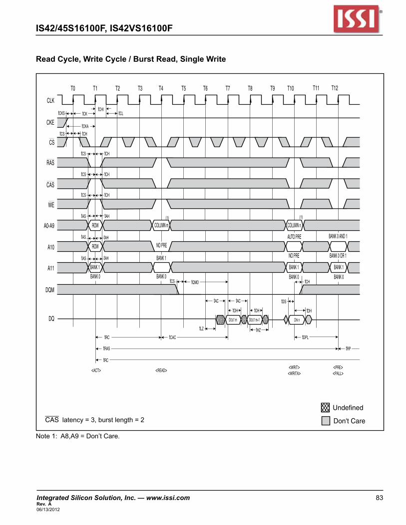
Integrated Silicon Solution, Inc. — www.issi.com 83Rev. A06/13/2012
IS42/45S16100F, IS42VS16100F
Read Cycle, Write Cycle / Burst Read, Single Write
CAS latency=3,burstlength=2
COLUMN n
CLK
CKE
CS
RAS
CAS
WE
A0-A9
A10
A11
DQM
DQ
T0 T1 T2 T3 T4 T5 T6 T7 T8 T9 T10
tCKtCHI
tCL
tCHtCS
tCHtCS
tCHtCS
tCHtCS
tAHtAS
BANK 1
BANK 0 AND 1
BANK 0 OR 1
NO PRE
NO PRE
AUTO PRE
tCH
tAHtAS
tCS
tAHtAS
tCKS
tCKA
BANK 0BANK 0
BANK 1
BANK 1
BANK 0
BANK 1
BANK 0
ROW COLUMN m
ROW
tQMD
tHZtLZ
tRAS
tRC
<ACT> <READ> <WRITA><WRIT>
<PALL><PRE>
tRC tCAC tDPL
tRP
tACtAC
tDH
tDS
tOH
DOUT m
tOH
DOUT m+1 DIN n
T11 T12
(1) (1)
Don't Care
Undefined
Note1:A8,A9=Don’tCare.
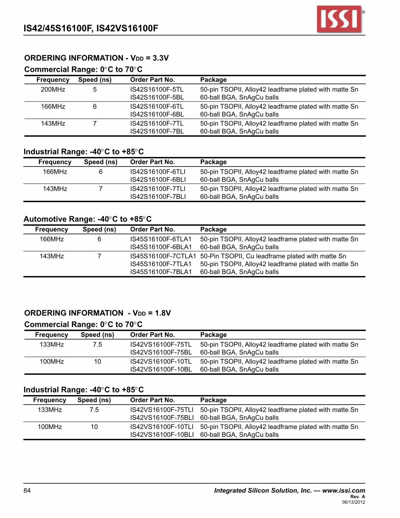
IS42/45S16100F, IS42VS16100F
84 Integrated Silicon Solution, Inc. — www.issi.com Rev. A
06/13/2012
ORDERING INFORMATION - VDD = 3.3VCommercial Range: 0°C to 70°C
Frequency Speed (ns) Order Part No. Package 200MHz 5 IS42S16100F-5TL 50-pinTSOPII,Alloy42leadframeplatedwithmatteSn IS42S16100F-5BL 60-ballBGA,SnAgCuballs 166MHz 6 IS42S16100F-6TL 50-pinTSOPII,Alloy42leadframeplatedwithmatteSn IS42S16100F-6BL 60-ballBGA,SnAgCuballs 143MHz 7 IS42S16100F-7TL 50-pinTSOPII,Alloy42leadframeplatedwithmatteSn IS42S16100F-7BL 60-ballBGA,SnAgCuballs
Industrial Range: -40°C to +85°C Frequency Speed (ns) Order Part No. Package 166MHz 6 IS42S16100F-6TLI 50-pinTSOPII,Alloy42leadframeplatedwithmatteSn IS42S16100F-6BLI 60-ballBGA,SnAgCuballs 143MHz 7 IS42S16100F-7TLI 50-pinTSOPII,Alloy42leadframeplatedwithmatteSn IS42S16100F-7BLI 60-ballBGA,SnAgCuballs
ORDERING INFORMATION - VDD = 1.8VCommercial Range: 0°C to 70°C
Frequency Speed (ns) Order Part No. Package 133MHz 7.5 IS42VS16100F-75TL 50-pinTSOPII,Alloy42leadframeplatedwithmatteSn IS42VS16100F-75BL 60-ballBGA,SnAgCuballs 100MHz 10 IS42VS16100F-10TL 50-pinTSOPII,Alloy42leadframeplatedwithmatteSn IS42VS16100F-10BL 60-ballBGA,SnAgCuballs
Industrial Range: -40°C to +85°C Frequency Speed (ns) Order Part No. Package 133MHz 7.5 IS42VS16100F-75TLI 50-pinTSOPII,Alloy42leadframeplatedwithmatteSn IS42VS16100F-75BLI 60-ballBGA,SnAgCuballs 100MHz 10 IS42VS16100F-10TLI 50-pinTSOPII,Alloy42leadframeplatedwithmatteSn IS42VS16100F-10BLI 60-ballBGA,SnAgCuballs
Automotive Range: -40°C to +85°C Frequency Speed (ns) Order Part No. Package 166MHz 6 IS45S16100F-6TLA1 50-pinTSOPII,Alloy42leadframeplatedwithmatteSn IS45S16100F-6BLA1 60-ballBGA,SnAgCuballs 143MHz 7 IS45S16100F-7CTLA1 50-PinTSOPII,CuleadframeplatedwithmatteSn IS45S16100F-7TLA1 50-pinTSOPII,Alloy42leadframeplatedwithmatteSn IS45S16100F-7BLA1 60-ballBGA,SnAgCuballs
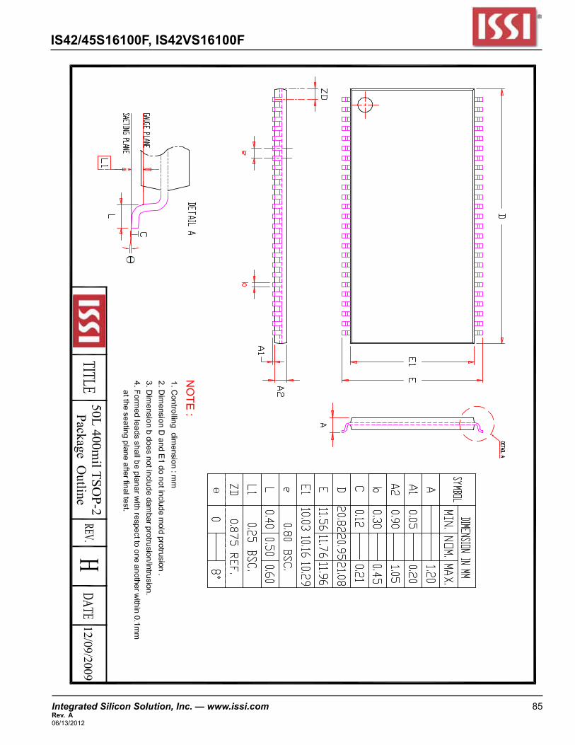
Integrated Silicon Solution, Inc. — www.issi.com 85Rev. A06/13/2012
IS42/45S16100F, IS42VS16100F
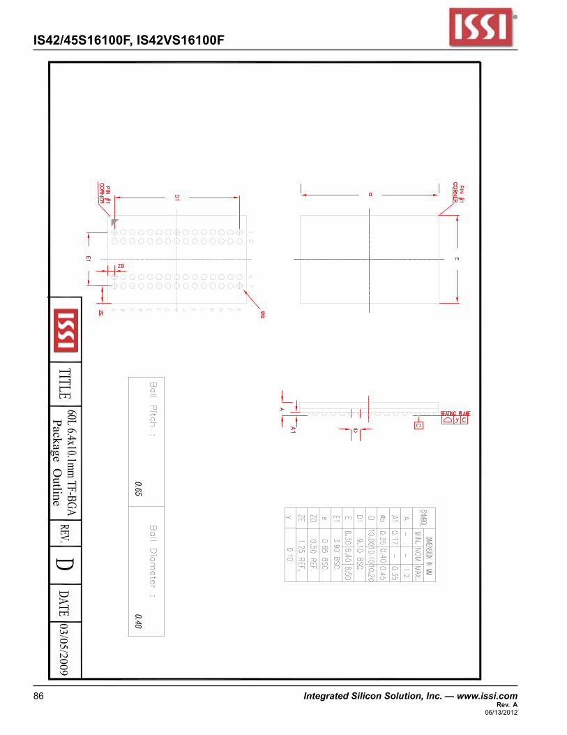
IS42/45S16100F, IS42VS16100F
86 Integrated Silicon Solution, Inc. — www.issi.com Rev. A
06/13/2012