Embed Size (px)
Citation preview

To learn more about ON Semiconductor, please visit our website at www.onsemi.com
Is Now Part of
ON Semiconductor and the ON Semiconductor logo are trademarks of Semiconductor Components Industries, LLC dba ON Semiconductor or its subsidiaries in the United States and/or other countries. ON Semiconductor owns the rights to a number of patents, trademarks, copyrights, trade secrets, and other intellectual property. A listing of ON Semiconductor’s product/patent coverage may be accessed at www.onsemi.com/site/pdf/Patent-Marking.pdf. ON Semiconductor reserves the right to make changes without further notice to any products herein. ON Semiconductor makes no warranty, representation or guarantee regarding the suitability of its products for any particular purpose, nor does ON Semiconductor assume any liability arising out of the application or use of any product or circuit, and specifically disclaims any and all liability, including without limitation special, consequential or incidental damages. Buyer is responsible for its products and applications using ON Semiconductor products, including compliance with all laws, regulations and safety requirements or standards, regardless of any support or applications information provided by ON Semiconductor. “Typical” parameters which may be provided in ON Semiconductor data sheets and/or specifications can and do vary in different applications and actual performance may vary over time. All operating parameters, including “Typicals” must be validated for each customer application by customer’s technical experts. ON Semiconductor does not convey any license under its patent rights nor the rights of others. ON Semiconductor products are not designed, intended, or authorized for use as a critical component in life support systems or any FDA Class 3 medical devices or medical devices with a same or similar classification in a foreign jurisdiction or any devices intended for implantation in the human body. Should Buyer purchase or use ON Semiconductor products for any such unintended or unauthorized application, Buyer shall indemnify and hold ON Semiconductor and its officers, employees, subsidiaries, affiliates, and distributors harmless against all claims, costs, damages, and expenses, and reasonable attorney fees arising out of, directly or indirectly, any claim of personal injury or death associated with such unintended or unauthorized use, even if such claim alleges that ON Semiconductor was negligent regarding the design or manufacture of the part. ON Semiconductor is an Equal Opportunity/Affirmative Action Employer. This literature is subject to all applicable copyright laws and is not for resale in any manner.
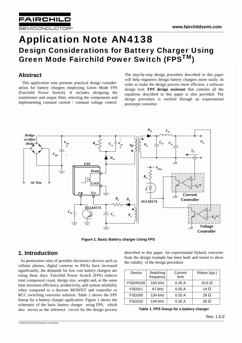
Application Note AN4138Design Considerations for Battery Charger Using Green Mode Fairchild Power Switch (FPSTM)
www.fairchildsemi.com
©2003 Fairchild Semiconductor Corporation
Abstract This application note presents practical design consider-ations for battery chargers employing Green Mode FPS(Fairchild Power Switch). It includes designing thetransformer and output filter, selecting the components andimplementing constant current / constant voltage control.
The step-by-step design procedure described in this paperwill help engineers design battery chargers more easily. Inorder to make the design process more efficient, a softwaredesign tool, FPS design assistant that contains all theequations described in this paper is also provided. Thedesign procedure is verified through an experimentalprototype converter.
Rev. 1.0.0
1. Introduction As penetration rates of portable electronics devices such ascellular phones, digital cameras or PDAs have increasedsignificantly, the demands for low cost battery chargers arerising these days. Fairchild Power Switch (FPS) reducestotal component count, design size, weight and, at the sametime increases efficiency, productivity, and system reliabilitywhen compared to a discrete MOSFET and controller orRCC switching converter solution. Table 1 shows the FPSlineup for a battery charger application. Figure 1 shows theschematic of the basic battery charger using FPS, whichalso serves as the reference circuit for the design process
described in this paper. An experimental flyback converterfrom the design example has been built and tested to showthe validity of the design procedure.
Table 1. FPS lineup for a battery charger
Figure 1. Basic Battery charger Using FPS
Np NSRsn Csn
-Vsn+
VDC+
-
AC line
Dsn
DR
CO
Drain
Vcc
GND
FB
FPS
Na
DaRa
Ca
H11A817A
Rd
Bridgerectifier
diode VO
LP
CP
CB
CDC
IO
IOref
VOref
CurrentController
VoltageController
Vbias
H11A817A
Device Switching frequency
Current limit
Rdson (typ.)
FSDH0165 100 kHz 0.35 A 15.6 ΩFSD311 67 kHz 0.55 A 14 ΩFSD200 134 kHz 0.32 A 28 ΩFSD210 134 kHz 0.32 A 28 Ω

AN4138 APPLICATION NOTE
2
©2002 Fairchild Semiconductor Corporation
2. Step-by-step Design Procedure
Figure 2. Flow chart of design procedure
In this section, a design procedure is presented using theschematic of Figure 1 as a reference. Figure 2 illustrates thedesign flow chart. The detailed design procedures are asfollows:
(1) STEP-1 : Define the system specifications
- Line voltage range (Vlinemin and Vline
max). - Line frequency (fL). - Maximum output power (Po). - Estimated efficiency (Eff) : It is required to estimate thepower conversion efficiency to calculate the maximum inputpower. In the case of a battery charger, the efficiency isrelatively low due to the low output voltage and loss in theoutput current sense resistor. The typical efficiency is about0.65-0.7.
With the estimated efficiency, the maximum input power isgiven by
(2) STEP-2 : Determine DC link capacitor (CDC) and the DC link voltage range.
It is typical to select the DC link capacitor as 2-3uF per wattof input power for universal input range (85-265Vrms) and1uF per watt of input power for European input range (195V-265Vrms). With the DC link capacitor chosen, the minimumlink voltage is obtained as
where Dch is the DC link capacitor charging duty ratiodefined as shown in Figure 3, which is typically about 0.2and Pin, Vline
min and fL are specified in step-1.
The maximum DC link voltage is given as
where Vlinemax is specified in step-1.
Figure 3. DC Link Voltage Waveform
1. Determine the system specifications(Vline
min, Vlinemax, fL, Po, Eff)
2. Determine DC link capacitor (CDC) and DC link voltage range
3. Determine the reflected output voltage(VRO)
6. Determine the proper core and theminimum primary turns (Np
min)
7. Determine the number of turns for eachoutput
8. Determine the wire diameter for eachwinding
9. Choose the proper rectifier diode for eachoutput
10. Determine the output capacitor
11. Design the RCD snubber
12. Control Circuit design
5. Choose proper FPS considering inputpower and Ids
peak
4. Determine the transformer primary sideinductance (Lm) and maximum duty (Dmax)
Is the winding windowarea (Aw) enough ?
Design finished
Y
N
Is it possible to change the core ?Y
N
PinPoEff-------= (1)
VDCmin 2 Vline
min( )⋅2 Pin 1 Dch–( )⋅
CDC fL⋅------------------------------------–= (2)
VDCmax 2Vline
max= (3)
DC link voltageMinimum DC link voltage
T1
T2Dch = T1 / T2
= 0.2
APPLICATION NOTE AN4138
3
©2002 Fairchild Semiconductor Corporation
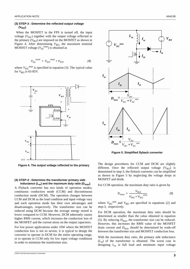
(3) STEP-3 : Determine the reflected output voltage (VRO).
When the MOSFET in the FPS is turned off, the inputvoltage (VDC) together with the output voltage reflected tothe primary (VRO) are imposed on the MOSFET as shown inFigure 4. After determining VRO, the maximum nominalMOSFET voltage (Vds
nom) is obtained as
where VDCmax is specified in equation (3). The typical value
for VRO is 65-85V.
Figure 4. The output voltage reflected to the primary
(4) STEP-4 : Determine the transformer primary side inductance (Lm) and the maximum duty ratio (Dmax).A Flyback converter has two kinds of operation modes;continuous conduction mode (CCM) and discontinuousconduction mode (DCM). The operation changes betweenCCM and DCM as the load condition and input voltage varyand each operation mode has their own advantages anddisadvantages, respectively. The transformer size can bereduced using DCM because the average energy stored islower compared to CCM. However, DCM inherently causeshigher RMS current, which increases the conduction loss ofthe MOSFET and the current stress on the output capacitors. For low power applications under 10W where the MOSFETconduction loss is not so severe, it is typical to design theconverter to operate in DCM for the entire operating range,or to operate in CCM only for low input voltage conditionsin order to minimize the transformer size.
Figure 5. Simplified flyback converter
The design procedures for CCM and DCM are slightlydifferent. Once the reflected output voltage (VRO) isdetermined in step-3, the flyback converter can be simplifiedas shown in Figure 5 by neglecting the voltage drops inMOSFET and diode.
For CCM operation, the maximum duty ratio is given by
where VDCmin and VRO are specified in equations (2) and
step-3, respectively.
For DCM operation, the maximum duty ratio should bedetermined as smaller than the value obtained in equation(5). By reducing Dmax, the transformer size can be reduced.However, this increases the RMS value of the MOSFETdrain current and Dmax should be determined by trade-offbetween the transformer size and MOSFET conduction loss.
With the maximum duty ratio, the primary side inductance(Lm) of the transformer is obtained. The worst case indesigning Lm is full load and minimum input voltage
Vdsnom VDC
max VRO+= (4)
-
V R O
+
V DC+
-
D rain
G N D
F PS
+
Vds-
0 V
V D C
V RO
Lm
VDCmin
VRO
Ids
ID
Im
Im
Im
Ids
Ids
Dmax
Dmax
ID
ID
minDCRO
RO
VVV+
=
minDCRO
RO
VVV+
≤
DmaxVRO
VRO VDCmin+
-------------------------------------= (5)

AN4138 APPLICATION NOTE
4
©2002 Fairchild Semiconductor Corporation
condition. Therefore, Lm is obtained in this condition as
where VDCmin is specified in equation (2), Dmax is specified
in equation (5), Pin is specified in step-1, fs is the switchingfrequency of the FPS device and KRF is the ripple factor infull load and minimum input voltage condition, defined asshown in Figure 6. For DCM operation, KRF = 1 and forCCM operation KRF < 1. The ripple factor is closely relatedto the transformer size and the RMS value of the MOSFETcurrent. In the case of low power applications such as batterychargers, a relatively large ripple factor is used in order tominimize the transformer size. It is typical to set KRF = 0.5-0.7 for the universal input range and KRF = 1.0 for theEuropean input range.
Once Lm is determined, the maximum peak current and RMScurrent of the MOSFET in normal operation are obtained as
where Pin, VDCmin, Dmax and Lm are specified in equations
(1), (2), (5) and (6) respectively and fs is the FPS switchingfrequency.
Figure 6. MOSFET Drain Current and Ripple Factor (KRF)
(5) STEP-5 : Choose the proper FPS considering input power and peak drain current.
With the resulting maximum peak drain current of theMOSFET (Ids
peak) from equation (7), choose the proper FPSof which the pulse-by-pulse current limit level (Iover) ishigher than Ids
peak. Since FPS has ± 12% tolerance of Iover,there should be some margin in choosing the proper FPSdevice.
(6) STEP-6 : Determine the proper core and the minimum primary turns.
Table 2 shows the commonly used cores for battery chargerswith output power under 10W. The cores recommended intable 2 are typical for the universal input range and 100kHzswitching frequency. With the chosen core, the minimum number of turns for thetransformer primary side to avoid the core saturation is givenby
where Lm is specified in equation (6), Iover is the FPS pulse-by-pulse current limit level, Ae is the cross-sectional area ofthe core as shown in Figure 7 and Bsat is the saturation fluxdensity in tesla. Figure 8 shows the typical characteristics offerrite core from TDK (PC40). Since the saturation fluxdensity (Bsat) decreases as the temperature goes high, thehigh temperature characteristics should be considered.If there is no reference data, use Bsat =0.3~0.35 T. Since theMOSFET drain current exceeds Ids
peak and reaches Iover in atransition or fault condition, Iover is used in equation (11)instead of Ids
peak to prevent core saturation during transition.
Figure 7. Window Area and Cross Sectional Area
LmVDC
min Dmax⋅( )2
2PinfsKRF----------------------------------------------= (6)
Idspeak IEDC
∆I2-----+= (7)
Idsrms 3 IEDC( )2 ∆I
2----- 2
+Dmax
3--------------= 8( )
IEDCPin
VDCmin Dmax⋅
--------------------------------------= (9)
∆IVDC
min DmaxLmfs
-----------------------------------= (10)
I∆ EDCI
EDCRF I
IK2
∆=
CCM operation : KRF < 1
I∆ EDCI
EDCRF I
IK2
∆=
DCM operation : KRF =1
peakdsI
peakdsI
NPmin LmIover
BsatAe------------------- 106 (turns)×= (11)
AwAwAwAw
AeAeAeAe

APPLICATION NOTE AN4138
5
©2002 Fairchild Semiconductor Corporation
Figure 8. Typical B-H characteristics of ferrite core (TDK/PC40)
Table 2. Typical cores for battery charger (For universal input range, 5V output and fs=100kHz)
(7) STEP-7 : Determine the number of turns for each outputFigure 9 shows the simplified diagram of the transformer.First, determine the turns ratio (n) between the primary sideand the secondary side.
where Np and Ns are the number of turns for primary sideand reference output, respectively, Vo is the output voltage,VF is the diode (DR) forward voltage drop and Vsense is themaximum voltage drop in the output current sensing resistor.
Then, determine the proper integer for Ns so that theresulting Np is larger than Np
min obtained from equation(11).
The number of turns for Vcc winding is determined as
where Vcc* is the nominal value of the supply voltage of theFPS device, and VFa is the forward voltage drop of Da asdefined in Figure 9. Since Vcc increases as the output loadincreases, it is proper to set Vcc* as Vcc start voltage (refer tothe data sheet) to avoid triggering the over voltage protectionduring normal operation.
Figure 9. Simplified diagram of the transformer
With the determined turns of the primary side, the gap lengthof the core is obtained as
where AL is the AL-value with no gap in nH/turns2, Ae is thecross sectional area of the core as shown in Figure 8, Lm isspecified in equation (6) and Np is the number of turns forthe primary side of the transformer
(8) STEP-8 : Determine the wire diameter for each winding based on the rms current of each output.
The rms current of the n-th secondary winding is obtained as
where VRO and Idsrms are specified in step-3 and equations
(8), Vo is the output voltage, VF is the diode (DR)) forwardvoltage drop and Dmax is specified in equation (5). The current density is typically 5A/mm2 when the wire is
Core Cross sectional area
Window area Output power range
EE13-Z 17.1 mm2 33.4 mm2 3-5W
EI16-Z 19.8 mm2 38.8 mm2 3-5W
EE16-Z 21.7 mm2 51.3 mm2 5-10W
EI19-Z 24.0 mm2 54.4 mm2 5-10W
100
500
400
300
200
800 16000
0Magnetic field H (A/m )
Flux
den
sity
B (m
T)
M agnetization Curves (typical)M aterial :PC40
100
120
60
25
nNPNs-------
VR0Vo VF Vsense+ +---------------------------------------------= = (12)
NaVcc* VFa+
Vo VF+----------------------------= Ns1⋅ turns( ) 13( )
Np
NS
-
VRO
+
DR
Na
Da+
VO
-
+ VF -- VFa +
+Vcc
*
-
- Vsense +
)( senseFos
pRO VVV
NN
V ++=
G 40πAeNP
2
1000Lm--------------------- 1
AL------–
= mm( ) 14( )
Isrms Ids
rms 1 Dmax–Dmax
-----------------------VRO
Vo VF+( )-------------------------⋅= 15( )

AN4138 APPLICATION NOTE
6
©2002 Fairchild Semiconductor Corporation
long (>1m). When the wire is short with a small number ofturns, a current density of 6-10 A/mm2 is also acceptable.Avoid using wire with a diameter larger than 1 mm to avoidsevere eddy current losses as well as to make winding easier. For high current output, it is better to use parallel windingswith multiple strands of thinner wire to minimize skin effect.
Check if the winding window area of the core, Aw (refer toFigure 8) is enough to accommodate the wires. Becausebobbin, insulation tape and gaps between wires, the wire cannot fill the entire winding window area. Typically the fillfactor is about 0.15-0.2 for a battery charger. Whenadditional dummy windings are employed for EMIshielding, the fill factor is reduced. The required windingwindow area (Awr) is given by
where Ac is the actual conductor area and KF is the fill factor.
If the required window (Awr) is larger than the actual windowarea (Aw), go back to the step-6 and change the core to abigger one. Sometimes it is impossible to change the coredue to cost or size constraints. If so, go back to step-4 andreduce Lm by increasing the ripple factor (KRF) or reducingthe maximum duty ratio. Then, the minimum number ofturns for the primary (Np
min) of the equation (11) willdecrease, which results in the reduced required windingwindow area (Awr).
(9) STEP-9 : Choose the rectifier diode in the secondary side based on the voltage and current ratings.The maximum reverse voltage and the rms current of theoutput rectifier diode (DR) are obtained as
where VDCmax, Dmax and Ids
rms are specified in equations(3), (5) and (8), respectively, Vo is the output voltage, VF isthe diode (DR) forward voltage and Vsense is the maximumvoltage drop in the output current sensing resistor.
The typical voltage and current margins for the rectifierdiode are as follows
where VRRM is the maximum reverse voltage and IF is theaverage forward current of the diode.A quick selection guide for Fairchild Semiconductor rectifierdiodes is given in table 3.
Table 3. Fairchild Diode quick selection table
(10) STEP-10 : Determine the output capacitor considering the voltage and current ripple.
The ripple current of the output capacitor (Co) is obtained as
where Io is the load current and IDrms is specified in equation
(18). The ripple current should be smaller than the ripplecurrent specification of the capacitor. The voltage ripple onthe n-th output is given by
where Co is the output capacitance, Rc is the effective seriesresistance (ESR) of the output capacitor, Dmax and Ids
peak arespecified in equations (5) and (7), respectively, Io and Vo arethe load current and output voltage, respectively, VF is thediode (DR) forward voltage and Vsense is the maximumvoltage drop in the output current sensing resistor. Sometimes it is impossible to meet the ripple specificationwith a single output capacitor due to the high ESR of theelectrolytic capacitor. Then, additional LC filter stages (postfilter) can be used. When using the post filters, be careful notto place the corner frequency too low. Too low a cornerfrequency may make the system unstable or limit the controlbandwidth. It is typical to set the corner frequency of thepost filter at around 1/10~1/5 of the switching frequency.
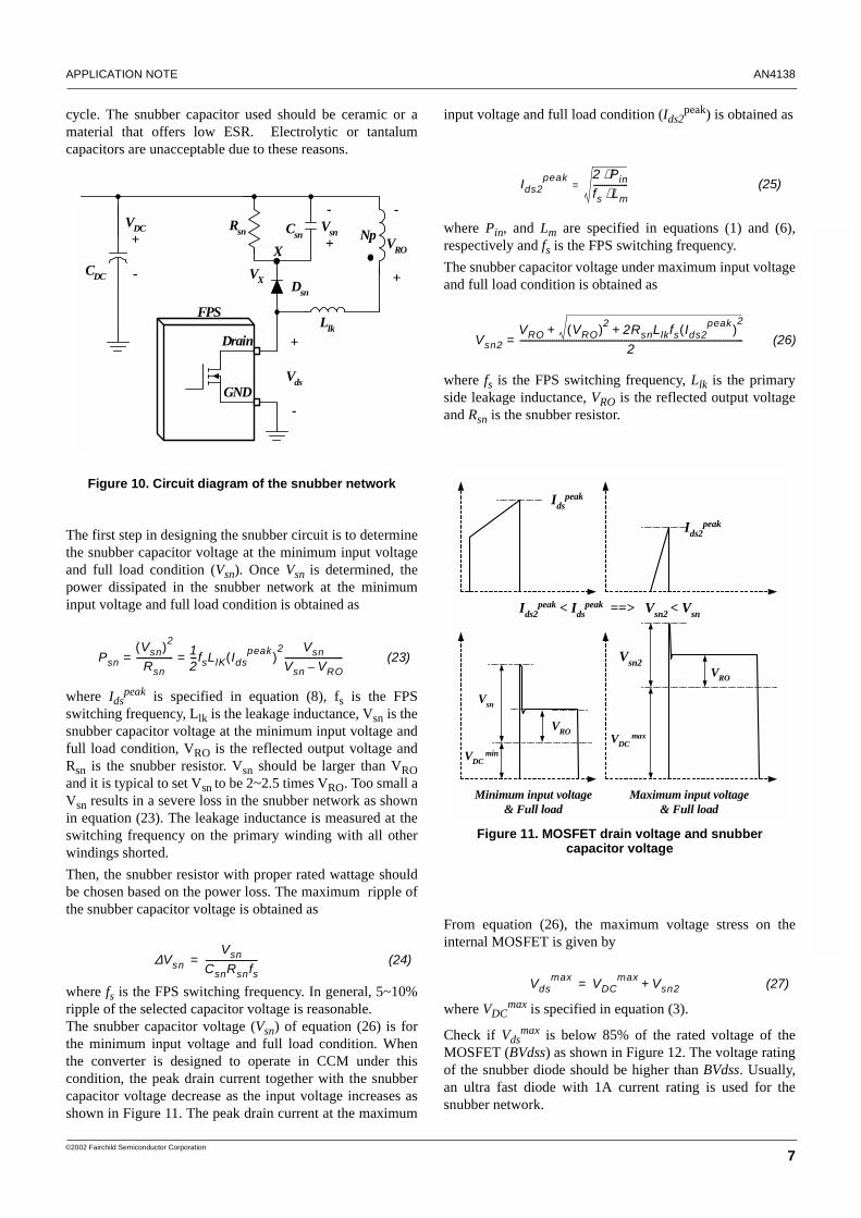
(11) STEP-11 : Design the RCD snubber.
When the power MOSFET is turned off, there is a highvoltage spike on the drain due to the transformer leakageinductance. This excessive voltage on the MOSFET maylead to an avalanche breakdown and eventually failure of theFPS. Therefore, it is necessary to use an additional networkto clamp the voltage.
The RCD snubber circuit and MOSFET drain voltagewaveform are shown in Figure 10 and 11, respectively. TheRCD snubber network absorbs the current in the leakageinductance by turning on the snubber diode (Dsn) once theMOSFET drain voltage exceeds the voltage of node X asdepicted in Figure 10. In the analysis of snubber network, itis assumed that the snubber capacitor is large enough that itsvoltage does not change significantly during one switching
Awr Ac KF⁄= (16)
VD VoVDC
max Vo VF Vsense+ +( )⋅VRO
---------------------------------------------------------------------------+= 17( )
IDrms Ids
rms VDCmin
VRO-------------------
VROVo VF Vsense+ +( )
-------------------------------------------------⋅= 18( )
VRRM 1.3 VD⋅> (19)
IF 1.5 IDrms⋅> (20)
Schottky Barrier DiodeProducts VRRM IF PackageSB340 40 V 3 A TO-210AD
SB350 50 V 3 A TO-210AD
SB360 60 V 3 A TO-210AD
Icaprms ID
rms( )2
Io2–= (21)
∆VoIoDmax
Cofs------------------
IdspeakVRORC
Vo VF Vsense+ +( )------------------------------------------------- (22)+=
APPLICATION NOTE AN4138
7
©2002 Fairchild Semiconductor Corporation
cycle. The snubber capacitor used should be ceramic or amaterial that offers low ESR. Electrolytic or tantalumcapacitors are unacceptable due to these reasons.
Figure 10. Circuit diagram of the snubber network
The first step in designing the snubber circuit is to determinethe snubber capacitor voltage at the minimum input voltageand full load condition (Vsn). Once Vsn is determined, thepower dissipated in the snubber network at the minimuminput voltage and full load condition is obtained as
where Idspeak is specified in equation (8), fs is the FPS
switching frequency, Llk is the leakage inductance, Vsn is thesnubber capacitor voltage at the minimum input voltage andfull load condition, VRO is the reflected output voltage andRsn is the snubber resistor. Vsn should be larger than VROand it is typical to set Vsn to be 2~2.5 times VRO. Too small aVsn results in a severe loss in the snubber network as shownin equation (23). The leakage inductance is measured at theswitching frequency on the primary winding with all otherwindings shorted.Then, the snubber resistor with proper rated wattage shouldbe chosen based on the power loss. The maximum ripple ofthe snubber capacitor voltage is obtained as
where fs is the FPS switching frequency. In general, 5~10%ripple of the selected capacitor voltage is reasonable. The snubber capacitor voltage (Vsn) of equation (26) is forthe minimum input voltage and full load condition. Whenthe converter is designed to operate in CCM under thiscondition, the peak drain current together with the snubbercapacitor voltage decrease as the input voltage increases asshown in Figure 11. The peak drain current at the maximum
input voltage and full load condition (Ids2peak) is obtained as
where Pin, and Lm are specified in equations (1) and (6),respectively and fs is the FPS switching frequency. The snubber capacitor voltage under maximum input voltageand full load condition is obtained as
where fs is the FPS switching frequency, Llk is the primaryside leakage inductance, VRO is the reflected output voltageand Rsn is the snubber resistor.
Figure 11. MOSFET drain voltage and snubber capacitor voltage
From equation (26), the maximum voltage stress on theinternal MOSFET is given by
where VDCmax is specified in equation (3).
Check if Vdsmax is below 85% of the rated voltage of the
MOSFET (BVdss) as shown in Figure 12. The voltage ratingof the snubber diode should be higher than BVdss. Usually,an ultra fast diode with 1A current rating is used for thesnubber network.
NpRsn Csn
-Vsn+
VDC+
-Dsn
Drain
GND
FPS
CDC
-
VRO
+
+
Vds
-
Llk
VX
X
PsnVsn( )2
Rsn----------------- 1
2---fsLlK Ids
peak( )2 VsnVsn VRO–---------------------------= = (23)
∆VsnVsn
CsnRsnfs------------------------= (24)
Ids2peak 2 Pin⋅
fs Lm⋅----------------= (25)
Vsn2VRO VRO( )2 2RsnLlkfs Ids2
peak( )2
++2
-------------------------------------------------------------------------------------------------------= (26)
VDC min
VRO
Vsn
VDC max
VRO
Vsn2
Idspeak
Ids2peak
Minimum input voltage& Full load
Maximum input voltage& Full load
Ids2peak < Ids
peak ==> Vsn2 < Vsn
Vdsmax VDC
max Vsn2+= (27)

AN4138 APPLICATION NOTE
8
©2003 Fairchild Semiconductor Corporation
In the snubber design in this section, neither the lossydischarge of the inductor nor stray capacitance is considered.In the actual converter, the loss in the snubber network is lessthan the designed value due to this effects.
Figure 12. MOSFET drain voltage and snubber capacitor voltage
(12) STEP-12 : Design the Control circuit.In general, a battery charger employs constant current (CC) /constant voltage (CV) control circuit for an optimal chargeof a battery. This design note presents two basic CC/CVcontrol circuits for FPS flyback converters. A simple, lowcost circuit using a transistor and shunt regulator (KA431) ispresented first. The second circuit features highly accuratecurrent control using an op amp together with a shuntregulator (KA431) and secondary bias winding. In the circuitanalysis, it is assumed that the CTR of the opto-coupler is100%.
(a) Transistor and regulator (KA431) schemeFigure 13 shows the CC/CV control circuit using a transistorand KA431 for 5.2V/0.65A output application. This circuit iswidely used when low cost and simplicity are majorconcerns. Since the transistor base-emitter voltage dropdepends on the temperature, a temperature compensationcircuit is required for temperature stability. To turn on thetransistor (Q), about 0.7V voltage drop across the sensingresistor (Rsense) is required and this current control circuitshould be used for output currents below 1A due to thepower dissipated in current sense resistor. For output currentsgreater than 1A, or if output current accuracy and
temperature stability are a key factor, the op amp currentcontrol circuits shown in Figure 15 should be used.
Figure 13. Transistor and KA431 CC/CV control
Constant voltage (CV) control : The voltage dividernetwork of R1 and R2 should be designed to provide 2.5V tothe reference pin of the KA431. The relationship between R1and R2 is given by
where Vo is the output voltage.By choosing R1 to be 2.2kΩ, R2 is obtained as
The feedback capacitor (CF) introduces an integrator for CVcontrol. To guarantee stable operation, CF of 470nF ischosen.The resistors Rbias and Rd should be designed to provideproper operating current for the KA431 and to guarantee thefull swing of the feedback voltage for the FPS device chosen.In general, the minimum cathode voltage and current for theKA431 are 2.5V and 1mA, respectively. Therefore, Rbias andRd should be designed to satisfy the following conditions.
0 V
VDC max
VRO
Vsn2
Effect of stray inductance (5-10V)BVdss
Voltage Margin > 10% of BVdss
NS
DR
CO
KA431
817A
Rd
Rbias
R1
R2
CF
VO
LP
CP
Rsense
Rbase
Q
RTH
CB
vFB
1:1
FPS
RB
GND
IFB
Io
250uA 510ΩΩΩΩ56ΩΩΩΩ
470nF
KSP2222
10kΩΩΩΩ
510ΩΩΩΩ
1ΩΩΩΩ
5.2V / 0.65A
2.2kΩΩΩΩ
2kΩΩΩΩ
R22.5 R1⋅Vo 2.5–---------------------= (28)
R22.5 2.2kΩ⋅5.2V 2.5V–------------------------------- 2kΩ= =
Vo VOP– 2.5–Rd
-------------------------------------- IFB> (29)
VOPRbias-------------- 1mA> (30)
APPLICATION NOTE AN4138
9
©2003 Fairchild Semiconductor Corporation
where Vo is the output voltage, VOP is opto-diode forwardvoltage drop, which is typically 1V and IFB is the feedbackcurrent of FPS. With IFB=0.25mA (FSD210), Rd and Rbiasare determined as 56Ω and 510Ω, respectively.
Constant Current (CC) control : The current controlcircuit is shown in detail in Figure 14. The CC control isimplemented using a transistor. Because the transistor base-emitter voltage drop varies with the temperature, negativethermal coefficient (NTC) thermistor is used for atemperature compensation.
Figure 14. Current control circuit in detail
When the voltage across the sensing resistor is sufficient toturn on the transistor, CC controller is enabled while CVcontroller is disabled. Then, the KA431 consumes very smallcurrent and most of the currents through Rd and Rbias flowinto the collector of the transistor Q. By assuming that thefeedback voltage of FPS (VFB) is in the middle of itsoperating range, half of the FPS feedback current (IFB) sinksinto the opto-coupler transistor. Since it is also assumed thatthe CTR of the opto-coupler is 100%, the transistor collectorcurrent is given by
where IFB is the feedback current of FPS, VOP is opto-diodeforward voltage drop, which is typically 1V.
From the circuit in Figure 14, IC is obtained as
By assuming that the current gain (β) of Q is 100, thetransistor base current is obtained as
The voltage drop in the sensing resistor (Vsense) should be setto be 40-100mV higher than the transistor base-emittervoltage (VBE) at room temperature (25°C). The actualtransistor base-emitter voltage (VBE) temperature ismeasured at room temperature as 0.608V with IC of 2.1mAand Vsense is determined to be 0.650V.
With the Vsense chosen, the sensing resistor (Rsense) isobtained as
where Io is SMPS output current.
It is typical to design the NTC thermistor so that the currentthrough the thermistor would be about 3-6 times of thetransistor base current at room temperature. The resistanceof the thermistor at room temperature (RTH) is determined as10 kΩ. The current through the thermistor is obtained as
The base resistor is determined by
Variations in the junction temperature of Q will causevariations in the value of controlled output current (Io). Thebase-emitter voltage decreases with increasing temperatureat a rate of approximately 2mV/°C. When the base-emittervoltage is changed to VBE
T as the temperature changes to T°C, the thermistor resistance at T °C required to compensatethis variation is given by
With -2mV/°C, VBE reduces to 0.508V from 0.608V astemperature increases from 25°C to 75°C. From equation
KA431
Rd Rbias
Rsense
RbaseQ
RTH
Io = 0.65A
510ΩΩΩΩ
56ΩΩΩΩ
KSP2222
10kΩΩΩΩ
510ΩΩΩΩ
1ΩΩΩΩ
IRTH
be
c
IFB /2
+VOP
-IC
IB
VBE
Vsense
ICIFB Rd⋅( ) 2⁄ Vop+
Rbias------------------------------------------------ 1
2--- IFB⋅+= (31)
IC250µA 56Ω⋅( ) 2⁄ 1V+
510Ω------------------------------------------------------------- 1
2--- 250µA⋅+ 2.1mA= =
IBICβ----- 2.1mA
100------------------ 21uA= = = (32)
RsenseVsense
Io------------------ 0.65V
0.65A---------------- 1Ω= = = (33)
IRTHVBERTH----------- 0.608V
10kΩ------------------- 61µA= = = (34)
RbaseVsense VBE–
VBERTH----------- IB+
---------------------------------- 0.65V 0.608V–0.608V10kΩ
------------------- 21µA+----------------------------------------- 513Ω= = = (35)
RTHT VBE
T
Vsense VBET–
Rbase-------------------------------------- IB–
-------------------------------------------------= (36)

AN4138 APPLICATION NOTE
10
©2003 Fairchild Semiconductor Corporation
(36), the resistance of the thermistor at 75°C to keep thesame output current is given by
NTC thermistor 103Χ2 from DSC is chosen for the compen-sation, whose resistance is 10kΩ at 25°C and 1.92kΩ at75°C.
(b) OP amp and shunt regulator (KA431) schemeFigure 15 shows a 4.2 V, 0.8A CC/CV control circuit usingthe LM358 dual op amp shunt regulator (KA431). Thiscircuit provides higher accuracy compared with the simpletransistor circuit. Power loss is lower and efficiency is betterbecause smaller resistance values can be used for senseresistor Rsense. The shunt regulator (KA431) is used as avoltage reference for an accurate control.
Constant voltage (CV) control : The Output voltage issensed by R1 and R2 and then compared by OP ampLM358B to reference of 2.5V. The output of the OP ampdrives current through D2 and Rd into the LED of the opto-coupler. The voltage divider network of R1 and R2 should bedesigned to provide 2.5V to the reference pin of the KA431.The relationship between R1 and R2 is given by
where Vo is the output voltage.By choosing R1 to be 680Ω, R2 is obtained as
CF2, RF2, and R6 compensate the voltage control loop.
Constant Current (CC) control : The voltage drop acrossthe sensing resistor (Rsense) is given by
It is typical to set Vsense as 0.1-0.2V. Since the inverting input of OP amp is virtually grounded,the relationship between R4 and R5 is given by
By choosing R5 as 33kΩ, R4 is obtained as 2.1kΩ. CF2, RF2, and R6 compensate the current control loop.
0.508V0.65V 0.508V–
513----------------------------------------- 21µA–-------------------------------------------------------------- 1.99k=
R22.5 R1⋅Vo 2.5–---------------------= (37)
R22.5 680⋅4.2V 2.5V–------------------------------- 1kΩ= =
Vsense IoRsense= 38( )
R4Vsense R5⋅
2.5-----------------------------= (39)

APPLICATION NOTE AN4138
11
©2003 Fairchild Semiconductor Corporation
Figure 15. CC/CV control using OP amp and shunt regulator
N S
D R
C O
H 11A 817A
R d
R 1
R 2
V O
L P
C P
R sense
D bias
C bias
V bias
R 3
KA 431VR EF=2.5V
R 4
R 5
C F1
C F2
LM 358A
LM 358B
1
3
2
4
8
5
67
IO
N bias
C B
vFB
1:1
F PS
R B
G N D
IFB
1N 4148
R F1
0.2 ΩΩΩΩ
4.2V
0.8A
680ΩΩΩΩ
1.0kΩΩΩΩ
4.7kΩΩΩΩR F2
4.7kΩΩΩΩ
0.1uF
1kΩΩΩΩ
R 6100kΩΩΩΩ
200ΩΩΩΩ
0.1uF
33kΩΩΩΩ
2.1kΩΩΩΩ
1N 4148
D 1
D 2

AN4138 APPLICATION NOTE
12
©2002 Fairchild Semiconductor Corporation
- Summary of symbols - Aw : Winding window area of the core in mm2
Ae : Cross sectional area of the core in mm2 Bsat : Saturation flux density in tesla. Co : Output capacitorDmax : Maximum duty cycle ratioEff : Estimated efficiencyfL : Line frequencyfs : Switching frequency of FPSIds
peak : Maximum value of peak current through MOSFET at the minimum input voltage conditionIds2
peak : Maximum value of peak current through MOSFET at the maximum input voltage conditionIds
rms : RMS current of MOSFETIds2 : Maximum peak drain current at the maximum input voltage condition.Iover : FPS current limit level.Ise
rms : RMS current of the secondary windingID
rms : Maximum rms current of the output rectifier diode Icap
rms : RMS Ripple current of the output capacitor Io : Output load current KRF : Current ripple factor Lm : Transformer primary side inductance Llk : Transformer primary side leakage inductance Losssn : Maximum power loss of the snubber network in normal operationNp
min : The minimum number of turns for the transformer primary side to avoid saturationNp : Number of turns for primary side windingNs : Number of turns for the output windingNa : Number of turns for the Vcc windingPo : Maximum output powerPin : Maximum input power Rc : Effective series resistance (ESR) of the output capacitor.Rsn : Snubber resistorRL : Effective total output load resistor of the controlled outputVline
min : Minimum line voltageVline
max : Maximum line voltageVDC
min : Minimum DC link voltage VDC
max : Maximum DC line voltageVds
nom : Maximum nominal MOSFET voltageVo : Output voltage VF : Forward voltage drop of the output rectifier diode. Vcc
* : Nominal voltage for VccVFa : Diode forward voltage drop of Vcc windingVD : Maximum voltage of the output rectifier diode VRO : Output voltage reflected to the primaryVsn : Snubber capacitor voltage under minimum input voltage and full load conditionVsn2 : Snubber capacitor voltage under maximum input voltage and full load condition Vds
max : Maximum voltage stress of the MOSFET

APPLICATION NOTE AN4138
13
©2002 Fairchild Semiconductor Corporation
The estimated efficiency (Eff) is set to be 0.65, considering the low output voltage and the loss in the current sensing resistor.
Design example using FPS Design Assistant
±±±± 5%
Ripple spec
5.2V (0.65A)85V-265VAC3.4WFSD210Battery charger
Output voltage (Max Current)Input voltageOutput Power
DeviceApplication
±±±± 5%
Ripple spec
5.2V (0.65A)85V-265VAC3.4WFSD210Battery charger
Output voltage (Max Current)Input voltageOutput Power
DeviceApplication
Since the input power is 5.2 W, the DC link capacitor is set to be 9.4uF by 2uF/Watt. (4.7uF××××2)
VRO is set to be 70V so that Vdsnom would be about 70% of 650V.
1. Define the system specifications1. Define the system specifications1. Define the system specifications1. Define the system specifications
Minimum Line voltage (Vlinemin) 85 V.rms
Maximum Line voltage (Vlinemax) 265 V.rms
Line frequency (fL) 60 Hz
VVVVo(n)o(n)o(n)o(n) IIIIo(n)o(n)o(n)o(n) PPPPo(n)o(n)o(n)o(n)
Output 5.2 V 0.65 A 3333 WWWW
Maximum output power (PMaximum output power (PMaximum output power (PMaximum output power (Poooo) =) =) =) = 3.43.43.43.4 WWWW
Estimated efficiency (Eff) 65 %
Maximum input power (PMaximum input power (PMaximum input power (PMaximum input power (Pinininin) =) =) =) = 5.25.25.25.2 WWWW
2. Determine DC link capacitor and DC link voltage range2. Determine DC link capacitor and DC link voltage range2. Determine DC link capacitor and DC link voltage range2. Determine DC link capacitor and DC link voltage range
DC link capacitor (CDC) 9.4 uF
Minimum DC link voltage (VMinimum DC link voltage (VMinimum DC link voltage (VMinimum DC link voltage (VDCDCDCDCminminminmin) =) =) =) = 84848484 VVVV
Maximum DC link voltage (VMaximum DC link voltage (VMaximum DC link voltage (VMaximum DC link voltage (VDCDCDCDCmaxmaxmaxmax)=)=)=)= 375375375375 VVVV
3. Determine Maximum duty ratio (Dmax) 3. Determine Maximum duty ratio (Dmax) 3. Determine Maximum duty ratio (Dmax) 3. Determine Maximum duty ratio (Dmax)
Output voltage reflected to primary (VRO)= 70 V
Maximum duty ratio (Dmax) 0.4560.4560.4560.456
Max nominal MOSFET voltage (VMax nominal MOSFET voltage (VMax nominal MOSFET voltage (VMax nominal MOSFET voltage (Vdsdsdsdsnomnomnomnom) =) =) =) = 445445445445 VVVV
4. Determine transformer primary inductance (Lm)4. Determine transformer primary inductance (Lm)4. Determine transformer primary inductance (Lm)4. Determine transformer primary inductance (Lm)
Switching frequency of FPS (fs) 134 kHz
Ripple factor (KRF) 0.66
Primary side inductance (LPrimary side inductance (LPrimary side inductance (LPrimary side inductance (Lmmmm) =) =) =) = 1597159715971597 uHuHuHuH
Maximum peak drain current (IMaximum peak drain current (IMaximum peak drain current (IMaximum peak drain current (Idsdsdsdspeakpeakpeakpeak) =) =) =) = 0.230.230.230.23 AAAA
RMS drain current (IRMS drain current (IRMS drain current (IRMS drain current (Idsdsdsdsrmsrmsrmsrms
) =) =) =) = 0.100.100.100.10 AAAA 63
Maximum DC link voltage in CCM (VMaximum DC link voltage in CCM (VMaximum DC link voltage in CCM (VMaximum DC link voltage in CCM (VDCDCDCDCCCMCCMCCMCCM)))) 143143143143 VVVV
I∆ EDCI
EDCRF I
IK2
∆=
)(1)(1
CCMKDCMK
RF
RF
<=

AN4138 APPLICATION NOTE
14
©2002 Fairchild Semiconductor Corporation
Ferrite core EE1616 is chosen (Ae=19.4 mm2)
The voltage drop in the sensing resistor (0.7V) is included in the diode voltage drop of the output diode.
(0.7V + 0.5V = 1.2V)
Since the winding for 5.2V is short with small number of turns, relatively large current density (> 5A/mm2) is allowed.
7. Determine the number of turns for each output7. Determine the number of turns for each output7. Determine the number of turns for each output7. Determine the number of turns for each output
VVVVo(n)o(n)o(n)o(n) VVVVF(n)F(n)F(n)F(n) # of turns# of turns# of turns# of turns
Vcc (Use Vcc start voltage)Vcc (Use Vcc start voltage)Vcc (Use Vcc start voltage)Vcc (Use Vcc start voltage) 12 V 0.8 V 18.018.018.018.0 => 18181818 TTTT1st output for feedback1st output for feedback1st output for feedback1st output for feedback 5.25.25.25.2 VVVV 1.2 V 9 => 9999 TTTT
VF : Forward voltage drop of rectifier diode Primary turns (NPrimary turns (NPrimary turns (NPrimary turns (Npppp)=)=)=)= 99999999 TTTT
--->enough turns--->enough turns--->enough turns--->enough turns
Ungapped AL value (AL) 1150 nH/T2
Gap length (G) ; center pole gap =Gap length (G) ; center pole gap =Gap length (G) ; center pole gap =Gap length (G) ; center pole gap = 0.130.130.130.13 mmmmmmmm
Schottky Barrier DiodeSB260 (60V/2A, VF=0.55V) output (5.2V)
Ultra Fast Recovery DiodeUF4003 (200V /1A, VF=1V)Vcc winding
Schottky Barrier DiodeSB260 (60V/2A, VF=0.55V) output (5.2V)
Ultra Fast Recovery DiodeUF4003 (200V /1A, VF=1V)Vcc winding
5. Choose the proper FPS considering the input power and current limit5. Choose the proper FPS considering the input power and current limit5. Choose the proper FPS considering the input power and current limit5. Choose the proper FPS considering the input power and current limit
Typical current limit of FPS (Iover) 0.32 A
Minimum IMinimum IMinimum IMinimum Ioveroveroverover considering tolerance of 12% considering tolerance of 12% considering tolerance of 12% considering tolerance of 12% 0.280.280.280.28 AAAA >>>> AAAA
->O.K.->O.K.->O.K.->O.K.
6. Determine the proper core and the minimum primary turns6. Determine the proper core and the minimum primary turns6. Determine the proper core and the minimum primary turns6. Determine the proper core and the minimum primary turns
Saturation flux density (Bsat) 0.30 T
Cross sectional area of core (Ae) 19.4 mm2
Minimum primary turns (NMinimum primary turns (NMinimum primary turns (NMinimum primary turns (Nppppminminminmin)=)=)=)= 87.887.887.887.8 TTTT
0.230.230.230.23
8. Determine the wire diameter for each winding 8. Determine the wire diameter for each winding 8. Determine the wire diameter for each winding 8. Determine the wire diameter for each winding
DiameterDiameterDiameterDiameter ParallelParallelParallelParallel IIIID(n)D(n)D(n)D(n)rmsrmsrmsrms (A/mm(A/mm(A/mm(A/mm2222))))
Primary windingPrimary windingPrimary windingPrimary winding 0.16 mm 1 T 0.10.10.10.1 AAAA 4.94.94.94.9Vcc windingVcc windingVcc windingVcc winding 0.16 mm 2 T 0.10.10.10.1 AAAA 2.52.52.52.5Output windingOutput windingOutput windingOutput winding 0.4 mm 1 T 1.21.21.21.2 AAAA 9.49.49.49.4
Copper area (ACopper area (ACopper area (ACopper area (Acccc) =) =) =) = 3.843.843.843.84 mmmmmmmm2222
Fill factor (KF) 0.15
Required window area (ARequired window area (ARequired window area (ARequired window area (Awrwrwrwr)))) 25.6225.6225.6225.62 mmmmmmmm2222
9. Choose the rectifier diode in the secondary side9. Choose the rectifier diode in the secondary side9. Choose the rectifier diode in the secondary side9. Choose the rectifier diode in the secondary side
VVVVD(n)D(n)D(n)D(n) IIIID(n)D(n)D(n)D(n)rmsrmsrmsrms
Vcc diodeVcc diodeVcc diodeVcc diode 80808080 VVVV 0.100.100.100.10 AAAA1st output diode1st output diode1st output diode1st output diode 39393939 VVVV 1.181.181.181.18 AAAA

APPLICATION NOTE AN4138
15
©2002 Fairchild Semiconductor Corporation
Since the output voltage ripple exceeds the ripple spec of ±±±± 5%, additional LC filter stage should be used.
330uF capacitor together with 3.9uH inductor are used for the post filter.
The snubber capacitor and snubber resistor are chosen as 1nF and 94kΩΩΩΩ (47kΩΩΩΩ××××2), respectively. The maximum voltage stress on the MOSFET is below 80% of BVdss (700V)
10. Determine the output capacitor 10. Determine the output capacitor 10. Determine the output capacitor 10. Determine the output capacitor
1st output capacitor1st output capacitor1st output capacitor1st output capacitor 330 uF 200 mΩ 1.01.01.01.0 AAAA 0.500.500.500.50 VVVV
ΔVΔVΔVΔVo(n)o(n)o(n)o(n)CCCCo(n)o(n)o(n)o(n) RRRRC(n)C(n)C(n)C(n) IIIIcap(n)cap(n)cap(n)cap(n)
11. Design RCD snubber11. Design RCD snubber11. Design RCD snubber11. Design RCD snubber
Primary side leakage inductance (Llk) 50 uH
Maximum Voltage of snubber capacitor (Vsn) 170 V
Maximum snubber capacitor voltage ripple 9 %
Snubber resistor (RSnubber resistor (RSnubber resistor (RSnubber resistor (Rsnsnsnsn)=)=)=)= 99.699.699.699.6
Snubber capacitor (CSnubber capacitor (CSnubber capacitor (CSnubber capacitor (Csnsnsnsn)=)=)=)= 0.80.80.80.8 nFnFnFnF 0.1581
Power loss in snubber resistor (PPower loss in snubber resistor (PPower loss in snubber resistor (PPower loss in snubber resistor (Psnsnsnsn)=)=)=)= 0.30.30.30.3 WWWW (In Normal Operation)(In Normal Operation)(In Normal Operation)(In Normal Operation)
Peak drain current at VPeak drain current at VPeak drain current at VPeak drain current at VDCDCDCDCmaxmaxmaxmax (I (I (I (Ids2ds2ds2ds2) =) =) =) = 0.220.220.220.22 AAAA
Max Voltage of Csn at VMax Voltage of Csn at VMax Voltage of Csn at VMax Voltage of Csn at VDCDCDCDCmax max max max (V(V(V(Vsn2sn2sn2sn2)=)=)=)= 167167167167 VVVV
Max Voltage stress of MOSFET (VMax Voltage stress of MOSFET (VMax Voltage stress of MOSFET (VMax Voltage stress of MOSFET (Vdsdsdsdsmaxmaxmaxmax)=)=)=)= 542542542542 VVVV

AN4138 APPLICATION NOTE
16
©2002 Fairchild Semiconductor Corporation
Design Summary
Features• High efficiency (>60% at Universal Input)• Low power consumption (<100mW at 240Vac) with no load• Low component count • Enhanced system reliability through various protection functions • Internal soft-start (3ms)• Frequency Modulation for low EMI
Key Design Notes• The constant voltage (CV) mode control is implemented with resistors, R8, R9, R10 and R12, shunt regulator, U2, feedback
capacitor, C9 and opto-coupler, U3. • Even though FSD210 has an internal soft start, C10 is employed to provide longer soft start time. Since C10 reduces the
feedback gain, a relatively small resistor is used for R9 in order to compensate it.• The constant current (CC) mode control is realized with resistors, R8, R9, R15, R16, R17 and R19, npn transistor, Q1 and
NTC, TH1. When the voltage across current sensing resistors, R15,R16 and R17 is 0.7V, the npn transistor turns on and the current through the opto coupler LED increases. This reduces the feedback voltage and duty ratio. Therefore, the output voltage decreases and the output current is kept constant.
• The NTC (negative thermal coefficient) is used to compensate the temperature characteristics of the transistor Q1.
Figure 16. The final schematic of the flyback converter
For FSD21xFor FSD21xFor FSD21xFor FSD21x
L3
4uH
C8330uF 16V
L1 330uH
R19510R
R8510R
D6
1N4148
R347k
TH1 10k
Vo
.
R15 3R0
R5
39R
Q1KSP2222A
1
U2TL431
D11N4007
R16 3R0
C9 470nF
TX1
R102.2k
C24.7uF 400V
0
3
C4100nF
H11A817BU3
R1 4.7k
4
C14.7UF 400V
C533uF 50V
7Fuse
1W, 10R
C6 152M-Y, 250Vac
D31N4007
8
H11A817B
2
1
R7
4.7M, 1/4W
AC
R17 3R0
D21N4007
D41N4007
R956R
D5UF4007
AC
0
R122k
C7330uF 16V
(5.2V/0.65A)
R447k
C104.7uF 50V
U1FSD210
8
5
7
1
4
2 3
Vstr
Vcc
Dra
in
GN
D
Vfb
GN
D
GN
D
D7
SB260
R6
4.7M 1/4W 0
C3102k 1kV

APPLICATION NOTE AN4138
17
©2002 Fairchild Semiconductor Corporation
Experimental VerificationIn order to show the validity of the design procedurepresented in this paper, the converter of the design examplehas been built and tested. All the circuit components are usedas designed in the design example and the detailedtransformer structure is shown in Figure 17. The windingspecifications and measured transformer characteristics areshown in table 4 and 5, respectively. The dummy winding(W3) is used as an EMI shield. This winding improves EMIcharacteristics by screening the radiation noise generatedfrom the primary winding.
Figure 17. Transformer structure
Table 4. Winding specifications
Table 5. The measured transformer characteristics
Figure 18 shows the FPS drain current and voltagewaveforms at the minimum input voltage and full loadcondition. As designed, the maximum peak drain current(Ids
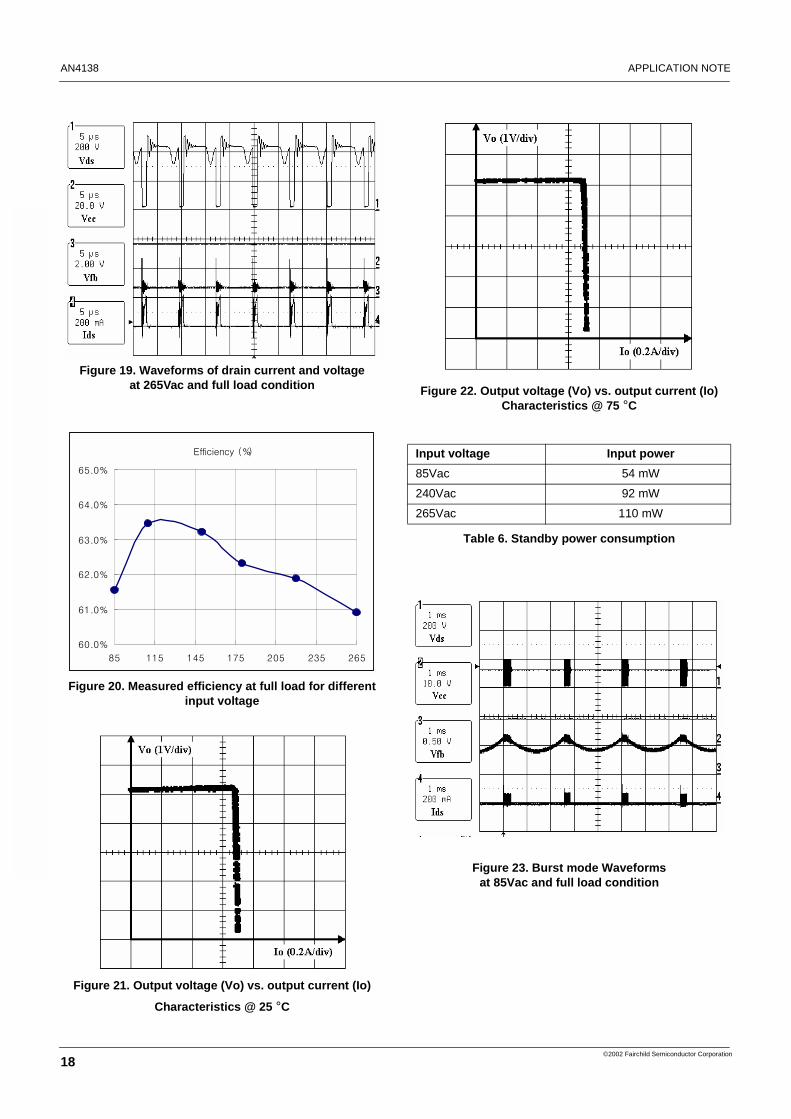
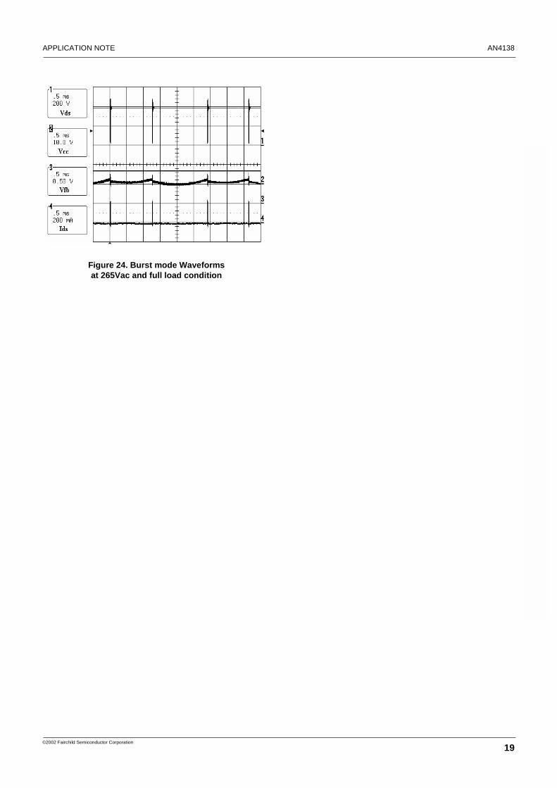
peak) is about 0.23A. Figure 19 shows the FPS draincurrent and voltage waveforms at the maximum inputvoltage and full load condition. The maximum voltage stresson the MOSFET is about 520V, which is lower than thedesigned value (542V). This is because of the lossydischarge of the inductor or the stray capacitance. Themeasured efficiencies at full load for different input voltagesare shown in Figure 20. The minimum efficiency is 61% at265V input voltage. The efficiencies are a little bit low dueto the power loss in the current sensing resistor in the output.The components for CC/CV control circuit are chosen asdesigned in design procedure of step-12. Figure 21 and 22show the output voltage vs. output current characteristics at25°C and 75°C, respectively. As designed, the outputvoltage is 5.2V and the output current is 0.65A. The outputcurrent variation with temperature is very small due to thetemperature compensation circuit with thermistor. Table 6 shows the power consumption in the standby mode.Through the burst mode operation, the power consumption isminimized. The power consumption at 240V input is under100 mW. The detailed burst operation waveforms are shownin Figure 23 and 24. By disabling and enabling the switchingoperation according to the feedback voltage, the effectiveswitching frequency is reduced, which also reduces thepower consumption in the standby mode.
Figure 18. Waveforms of drain current and voltage at 85Vac and full load condition
1111
2222
3333
4444
8888
7777
6666
5555
W4
W3
W2
W1
2mm 2mm
INSULATION : POLYESTER TAPE t=0.025mm / 10mm, 3Ts
SOLENOID WINDING9 Ts0.40Φ Χ 18 → 7W4
INSULATION : POLYESTER TAPE t=0.025mm / 10mm, 3Ts
SOLENOID WINDING50 Ts0.16Φ Χ 11 → openW3
INSULATION : POLYESTER TAPE t=0.025mm / 10mm, 2Ts
CENTER SOLENOID WINDING
18 Ts0.16Φ Χ 14 → 3W2
INSULATION : POLYESTER TAPE t=0.025mm / 10mm, 2Ts
SOLENOID WINDING99 Ts0.16Φ Χ 11 → 2W1
Winding MethodWinding MethodTurnsTurnsWireWirePin (S Pin (S →→→→→→→→ F)F)No.No.
INSULATION : POLYESTER TAPE t=0.025mm / 10mm, 3Ts
SOLENOID WINDING9 Ts0.40Φ Χ 18 → 7W4
INSULATION : POLYESTER TAPE t=0.025mm / 10mm, 3Ts
SOLENOID WINDING50 Ts0.16Φ Χ 11 → openW3
INSULATION : POLYESTER TAPE t=0.025mm / 10mm, 2Ts
CENTER SOLENOID WINDING
18 Ts0.16Φ Χ 14 → 3W2
INSULATION : POLYESTER TAPE t=0.025mm / 10mm, 2Ts
SOLENOID WINDING99 Ts0.16Φ Χ 11 → 2W1
Winding MethodWinding MethodTurnsTurnsWireWirePin (S Pin (S →→→→→→→→ F)F)No.No.
Core EE1616 (ISU Ceramics)
Primary side inductance
1.6 mH @ 100kHz
Leakage inductance
50 uH @100kHz with all other windings shorted.
AN4138 APPLICATION NOTE
18
©2002 Fairchild Semiconductor Corporation
Figure 19. Waveforms of drain current and voltage at 265Vac and full load condition
Figure 20. Measured efficiency at full load for different input voltage
Figure 21. Output voltage (Vo) vs. output current (Io)
Characteristics @ 25 °C
Figure 22. Output voltage (Vo) vs. output current (Io)Characteristics @ 75 °C
Table 6. Standby power consumption
Figure 23. Burst mode Waveforms at 85Vac and full load condition
Efficiency (%)
60.0%
61.0%
62.0%
63.0%
64.0%
65.0%
85 115 145 175 205 235 265
Input voltage Input power85Vac 54 mW
240Vac 92 mW
265Vac 110 mW
APPLICATION NOTE AN4138
19
©2002 Fairchild Semiconductor Corporation
Figure 24. Burst mode Waveforms at 265Vac and full load condition
AN4138 APPLICATION NOTE
3/24/04 0.0m 002 2003 Fairchild Semiconductor Corporation
DISCLAIMER FAIRCHILD SEMICONDUCTOR RESERVES THE RIGHT TO MAKE CHANGES WITHOUT FURTHER NOTICE TO ANY PRODUCTS HEREIN TO IMPROVE RELIABILITY, FUNCTION OR DESIGN. FAIRCHILD DOES NOT ASSUME ANY LIABILITY ARISING OUT OF THE APPLICATION OR USE OF ANY PRODUCT OR CIRCUIT DESCRIBED HEREIN; NEITHER DOES IT CONVEY ANY LICENSE UNDER ITS PATENT RIGHTS, NOR THE RIGHTS OF OTHERS.
LIFE SUPPORT POLICY FAIRCHILD’S PRODUCTS ARE NOT AUTHORIZED FOR USE AS CRITICAL COMPONENTS IN LIFE SUPPORT DEVICES OR SYSTEMS WITHOUT THE EXPRESS WRITTEN APPROVAL OF THE PRESIDENT OF FAIRCHILD SEMICONDUCTOR CORPROATION. As used herein:
1. Life support devices or systems are devices or systems which, (a) are intended for surgical implant into the body, or (b) support or sustain life, or (c) whose failure to perform when properly used in accordance with instructions for use provided in the labeling, can be reasonably expected to result in significant injury to the user.
2. A critical component is any component of a life support device or system whose failure to perform can be reasonably expected to cause the failure of the life support device or system, or to affect its safety or effectiveness.
www.fairchildsemi.com
by Hang-Seok Choi / Ph. D
Power Supply Group / Fairchild SemiconductorPhone : +82-32-680-1383 Facsimile : +82-32-680-1317E-mail : [email protected]

www.onsemi.com1
ON Semiconductor and are trademarks of Semiconductor Components Industries, LLC dba ON Semiconductor or its subsidiaries in the United States and/or other countries.ON Semiconductor owns the rights to a number of patents, trademarks, copyrights, trade secrets, and other intellectual property. A listing of ON Semiconductor’s product/patentcoverage may be accessed at www.onsemi.com/site/pdf/Patent−Marking.pdf. ON Semiconductor reserves the right to make changes without further notice to any products herein.ON Semiconductor makes no warranty, representation or guarantee regarding the suitability of its products for any particular purpose, nor does ON Semiconductor assume any liabilityarising out of the application or use of any product or circuit, and specifically disclaims any and all liability, including without limitation special, consequential or incidental damages.Buyer is responsible for its products and applications using ON Semiconductor products, including compliance with all laws, regulations and safety requirements or standards,regardless of any support or applications information provided by ON Semiconductor. “Typical” parameters which may be provided in ON Semiconductor data sheets and/orspecifications can and do vary in different applications and actual performance may vary over time. All operating parameters, including “Typicals” must be validated for each customerapplication by customer’s technical experts. ON Semiconductor does not convey any license under its patent rights nor the rights of others. ON Semiconductor products are notdesigned, intended, or authorized for use as a critical component in life support systems or any FDA Class 3 medical devices or medical devices with a same or similar classificationin a foreign jurisdiction or any devices intended for implantation in the human body. Should Buyer purchase or use ON Semiconductor products for any such unintended or unauthorizedapplication, Buyer shall indemnify and hold ON Semiconductor and its officers, employees, subsidiaries, affiliates, and distributors harmless against all claims, costs, damages, andexpenses, and reasonable attorney fees arising out of, directly or indirectly, any claim of personal injury or death associated with such unintended or unauthorized use, even if suchclaim alleges that ON Semiconductor was negligent regarding the design or manufacture of the part. ON Semiconductor is an Equal Opportunity/Affirmative Action Employer. Thisliterature is subject to all applicable copyright laws and is not for resale in any manner.
PUBLICATION ORDERING INFORMATIONN. American Technical Support: 800−282−9855 Toll FreeUSA/Canada
Europe, Middle East and Africa Technical Support:Phone: 421 33 790 2910
Japan Customer Focus CenterPhone: 81−3−5817−1050
www.onsemi.com
LITERATURE FULFILLMENT:Literature Distribution Center for ON Semiconductor19521 E. 32nd Pkwy, Aurora, Colorado 80011 USAPhone: 303−675−2175 or 800−344−3860 Toll Free USA/CanadaFax: 303−675−2176 or 800−344−3867 Toll Free USA/CanadaEmail: [email protected]
ON Semiconductor Website: www.onsemi.com
Order Literature: http://www.onsemi.com/orderlit
For additional information, please contact your localSales Representative
© Semiconductor Components Industries, LLC