Embed Size (px)
Citation preview

To learn more about ON Semiconductor, please visit our website at www.onsemi.com
Is Now Part of
ON Semiconductor and the ON Semiconductor logo are trademarks of Semiconductor Components Industries, LLC dba ON Semiconductor or its subsidiaries in the United States and/or other countries. ON Semiconductor owns the rights to a number of patents, trademarks, copyrights, trade secrets, and other intellectual property. A listing of ON Semiconductor’s product/patent coverage may be accessed at www.onsemi.com/site/pdf/Patent-Marking.pdf. ON Semiconductor reserves the right to make changes without further notice to any products herein. ON Semiconductor makes no warranty, representation or guarantee regarding the suitability of its products for any particular purpose, nor does ON Semiconductor assume any liability arising out of the application or use of any product or circuit, and specifically disclaims any and all liability, including without limitation special, consequential or incidental damages. Buyer is responsible for its products and applications using ON Semiconductor products, including compliance with all laws, regulations and safety requirements or standards, regardless of any support or applications information provided by ON Semiconductor. “Typical” parameters which may be provided in ON Semiconductor data sheets and/or specifications can and do vary in different applications and actual performance may vary over time. All operating parameters, including “Typicals” must be validated for each customer application by customer’s technical experts. ON Semiconductor does not convey any license under its patent rights nor the rights of others. ON Semiconductor products are not designed, intended, or authorized for use as a critical component in life support systems or any FDA Class 3 medical devices or medical devices with a same or similar classification in a foreign jurisdiction or any devices intended for implantation in the human body. Should Buyer purchase or use ON Semiconductor products for any such unintended or unauthorized application, Buyer shall indemnify and hold ON Semiconductor and its officers, employees, subsidiaries, affiliates, and distributors harmless against all claims, costs, damages, and expenses, and reasonable attorney fees arising out of, directly or indirectly, any claim of personal injury or death associated with such unintended or unauthorized use, even if such claim alleges that ON Semiconductor was negligent regarding the design or manufacture of the part. ON Semiconductor is an Equal Opportunity/Affirmative Action Employer. This literature is subject to all applicable copyright laws and is not for resale in any manner.

Application Note AN6016LCD Backlight Inverter Drive IC (FAN7311)
REV. 1.0.1 4/20/06
tm
www.fairchildsemi.com
1. Description Design goals for a Cold Cathode Fluorescent Lamp (CCFL)inverter for use in a notebook computer or other portableapplications include small size, high efficiency, and low cost.The FAN7311 provides the necessary circuit blocks toimplement a highly efficient CCFL backlight power supplyin 20-SSOP and 20-SOIC packages. The FAN7311 typicallyconsumes less than 4mA of operating current, improvingoverall system efficiency. External parts count is minimizedand system cost is reduced by the integration of featuresincluding; feedback-controlled Pulse Width Modulation
(PWM) driver stage, soft start, open lamp regulation, andUnder Voltage Lockout protection (UVLO). The FAN7311includes an internal shunt regulator that allows operationwith an input voltage from 5V to 25.5V. It supports analogand burst dimming modes of operation. The FAN7311 pro-vides open lamp regulation and protection. Open lamp regu-lation protects the transformer from over-voltage during startup or when an open lamp occurs. The transformer voltage isregulated by reducing duty cycle when an over-voltage isdetected. Open lamp protection can be used to shut down anIC when an open lamp condition continues longer than aspecified time.
Figure 1. Application Circuit
0
OLP1 OLP2
R161k
D3BAV70
R171k
0
0
C1115p
0C3010n
0 0
C2
1 μ
TX1
0
0
C2110n
J1
0
R6
82k
C8 10μ
C251μ
0
0
0
0
D9
BAV99
C2810n
D7
BAV99
D6
BAV99
0
0
0
OUTA
R99.1k
0
0
1
2
HOT1
COLD
HOT
COLD
HOT
COLD
HOT
COLD
2
CN2CCFL
CN3CCFL
CN4CCFL
CN1CCFL
1
2
1
2
C22220μ25V
OLR
C26
1μ 0
RT
OLP
SN
GN
SP
GP DP
DP
DN
DN
M2
FDS8958A
FDS8958A
REF
R14100k
OUTB
D1
D10
D11
BAW56
BAW56
BAW56
RT
FB
R1330k
LTM190EXC6
1μ
0OLP2OLP1
OLP3 OLP4
R121k
R111k
R261k
REF
R131k
0 0
0 0
R15
10k
C91μ
F1
FUSE
C7 10μ
12345678910
CN5
12505WR-10
R24
10k
R25
10k
C1015p
C1410n
C1215p
C2910n
IC1 FAN7311
S_S
GND
REF
OLR
ENA
BDIM
OLP
VIN
OUTA
PGND
OUTB
RT1
CT
OUTC
ADIM
EA_IN
EA_OUT
OUTD
RT
BCT
R2210k
R2810k
C192.2n
C202.2n
00
0
0
R21R2010k 10k
C182.2n
C172.2n
0
R8
100k
Q1
KST2222
C1510n
0
C271μ
0
0
R181k
R70
0
SN
GN
SP
GP DP
DP
DN
DN
M1
FB
0
TX2
0
C1315p
0
OLP3 OLP4
R191k
OLR
R27
10k
ON/OFF
12V
DIM (0~3.3V)
0
C4 4.7n
C5 220p
R527k
0
R256k
R318k
R4
22k
0
0
C3
4.7n
D4BAV70
C1
0.22μ
D8
BAV99
0
0
OLR
FB
0.

AN6016 APPLICATION NOTE
2 REV. 1.0.1 4/20/06
2. Block Diagram and Basic Operation
2.1 Block Diagram
Figure 2. Block Diagram
BDIM
S_S
EA_OUT
OSCILLATORRT
Error Amp.
EA_IN
6μA
-
+
CT
max. 2V
min. 0.5V
ADIM
OUTB
OUTA
OUTC
OUTD
VIN
2.5VREF
ENA
UVLO 5VUVLO
REF
BCT
+
-
max. 2V
min. 0.5V
OLR
-
+
2V
1.4V
Solr
Q
Q SET
CLR
S
R UVLO
OLP
-
+
PGND
Sburst
Voltage Reference
&Internal
Bias
VIN
1.4μAUVLO
Output Driver
Output Control Logic
AGND
Solr 105μA
Sburst 85μA
Output Driver
+
+
- 2.5V
Va+α
RT1MRT1
VOLP
VOLP+α
2.5V 1.5V
StrikingLogic
OLP
S_S
1mA
-
+
-
+

REV. 1.0.1 4/20/06 3
AN6016 APPLICATION NOTE
2.2 Under Voltage Lockout (UVLO) The UVLO circuit guarantees stable operation of the IC’scontrol circuit by stopping and starting it as a function of theVIN value. The UVLO circuit turns on the control circuitwhen VIN exceeds 5V. When VIN is lower than 5V, the IC’sstandby current is less than 200µA.
2.3 ENA Applying voltage higher than 2V to ENA pin enables theoperation of the IC. Applying voltage lower than 0.7V toENA pin disables the operation of the inverter.
Figure 3. Under Voltage Lockout and ENA Circuits
Figure 4. Start Voltage and Operating Current
2.4 Soft Start The soft-start function is provided by the S_S pin and is con-nected through a capacitor to GND. A soft-start circuitensures a gradual increase in the input and output power. Thecapacitor connected to S_S pin determines the rise rate of theduty ratio. It is charged by a current source of 6µA.
Figure 5. Soft Start During Initial Operation
2.5 Oscillator
2.5.1 Main Oscillator
Timing capacitor CT is charged by the reference currentsource. The source is formed by the timing resistor RT whosevoltage is regulated at 1.25V. The sawtooth waveform of themain oscillator circuit charges up to 2V, then the capacitorbegins discharging down to 0.5V. The capacitor starts charg-ing again and a new switching cycle begins.
The main frequency can be programmed by adjusting thevalues of RT and CT. The main frequency can be calculatedas shown below.
Figure 6a. Main Oscillator Circuit
VIN
2.5VREF
ENA
UVLO 5V
+
-
+
-UVLO
REF
1.4V
VoltageReference
&Internal
Bias
VIN
VIN
Icc (mA)
4
2
05 10 15 20
(V)
Ich earg34--- 1.25
RT----------= (2.1)
fop19
32 RTCT----------------------= (2.2)
2VIcharge
20 x Icharge
0.5V
CT
+
-
+
-Q
QSET
CLR
S
R
AN6016 APPLICATION NOTE
4 REV. 1.0.1 4/20/06
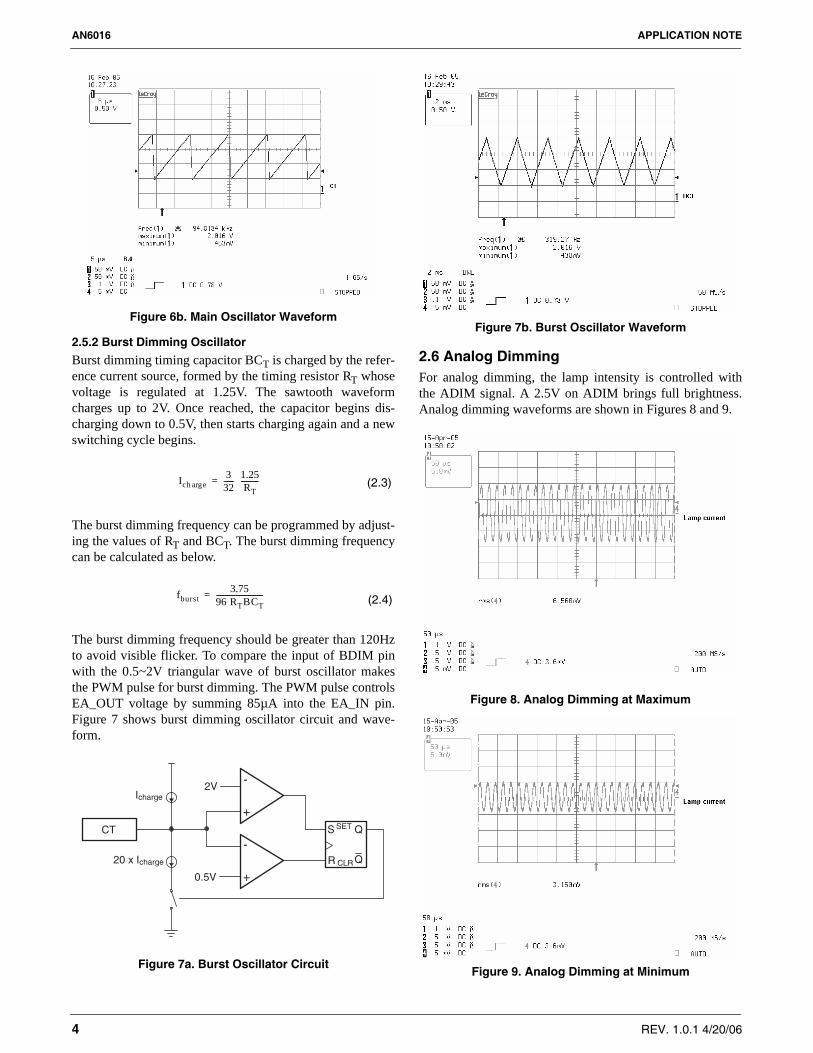
Figure 6b. Main Oscillator Waveform
2.5.2 Burst Dimming Oscillator
Burst dimming timing capacitor BCT is charged by the refer-ence current source, formed by the timing resistor RT whosevoltage is regulated at 1.25V. The sawtooth waveformcharges up to 2V. Once reached, the capacitor begins dis-charging down to 0.5V, then starts charging again and a newswitching cycle begins.
The burst dimming frequency can be programmed by adjust-ing the values of RT and BCT. The burst dimming frequencycan be calculated as below.
The burst dimming frequency should be greater than 120Hzto avoid visible flicker. To compare the input of BDIM pinwith the 0.5~2V triangular wave of burst oscillator makesthe PWM pulse for burst dimming. The PWM pulse controlsEA_OUT voltage by summing 85µA into the EA_IN pin.Figure 7 shows burst dimming oscillator circuit and wave-form.
Figure 7a. Burst Oscillator Circuit
Figure 7b. Burst Oscillator Waveform
2.6 Analog Dimming For analog dimming, the lamp intensity is controlled withthe ADIM signal. A 2.5V on ADIM brings full brightness.Analog dimming waveforms are shown in Figures 8 and 9.
Figure 8. Analog Dimming at Maximum
Figure 9. Analog Dimming at Minimum
(2.3)Ich earg332------ 1.25
RT----------=
(2.4)fburst3.75
96 RTBCT--------------------------=
2VIcharge
20 x Icharge
0.5V
CT
+
-
+
-Q
QSET
CLR
S
R

REV. 1.0.1 4/20/06 5
AN6016 APPLICATION NOTE
2.6.1 Setting Lamp Current Sensing Resistors
1) Positive Polarity Analog Dimming
Figure 10. Calculating Value of the Analog Dimming Circuit Parameter
Lamp current is sensed at Rsense and the sensed voltage isdivided by RCS1 and RCS2 and is averaged at Error Amp. byRFB and CFB.
Equation (2.5) assumes that the error amplifier loop isclosed. The relationship between VCS and Vref is given inequation (2.6).
From these values, an approximate value of Rcs2 can bederived. To get a more precise value for RCS2, use an itera-tive calculation. Use Rsense to calculate RCS2, because theRsense_eq value is unknown. After finding the value ofRsense_eq, use Rsense_eq to calculate RCS2. Calculate itera-tively until the previous Rsense_eq value is almost equal to thecurrent Rsense_eq value.
Rsense_effective 0.950148969kΩ = Rsense/(RCS1+RCS2)
2) Negative Polarity Analog Dimming
Figure 11. Calculating Value of the Analog Dimming Inverting Circuit Parameter
Lamp current is sensed at Rsense and the sensed voltage isdivided by Rcs1 and Rcs2 and is averaged at Error Amp. byRFB and CFB.
Equation (2.8) assumes the error amplifier loop is closed.The relationship between VCS and VA (dimming controlvoltage) is given in equation (2.9).
CFB
RFBVCS Vsense
Rsense
Rsense
CCFL CCFLRCS1
RCS2ErrorAmp.
VREF+
–
Rsense_eq
1VDF
Ilamp Rcs1 Rcs2+( )⋅-------------------------------------------------+
R----------------------------------------------------------- Rsense Rcs1 Rcs2+( ) ,||≈=
VDF is diode forward voltage
Vsense1π--- 2
0
π
∫ ILamp Rsense_eq θsin dθ⋅ ⋅ ⋅ ⋅⎝ ⎠⎜ ⎟⎛ ⎞
VDF–=
2π--- 2 ILamp Rsense_eq⋅ VDF 1( )–⋅ ⋅=
VCS VsenseRcs2
Rcs1 Rcs2+----------------------------⋅ 2π--- 2 ILamp Rsense VDF–⋅ ⋅ ⋅⎝ ⎠
⎛ ⎞= =
(2.5)Rcs2
Rcs1 Rcs2+----------------------------⋅
Vref VCS VsenseRcs2
Rcs1 Rcs2+----------------------------⋅= =
2π--- 2 ILamp Rsense⋅ VDF–⋅ ⋅⎝ ⎠
⎛ ⎞ Rcs2Rcs1 Rcs2+----------------------------⋅= (2.6)
Rcs1Rcs2----------
VsenseVref
--------------- 1–= (2.7)
For example, suppose:
Vref 2.5V, ILamp 6.5mA, Rsense 1kΩ Rcs1, 10kΩ= = = =
The data to inputThe calculated data
VREF 2.5 Ilamp 6.5 Rsense 1 kΩ
Rsense_eff 0.95 kΩDiode drop voltage 0.3 V
Vsense 5.259453252 V RCS1/RCS2 1.103781301
RCS1 10 kΩRCS2 9.059765727 kΩ
CFB
RFBVCS
VAVsense
Rsense
Rsense
CCFL CCFL
RCS1
RCS2ErrorAmp.
VREF+
–
Rsense_eq
1VDF
Ilamp Rcs1 Rcs2+( )⋅-------------------------------------------------+
R----------------------------------------------------------- Rsense Rcs1 Rcs2+( ) ,||≈=
VDF is diode forward voltage
Vsense1π--- 2
0
π
∫ ILamp Rsense_eq θsin dθ⋅ ⋅ ⋅ ⋅⎝ ⎠⎜ ⎟⎛ ⎞
VDF–=
2π--- 2 ILamp Rsense_eq⋅ VDF 1( )–⋅ ⋅=
VCS VsenseRcs2
Rcs1 Rcs2+----------------------------⋅ 2π--- 2 ILamp Rsense VDF–⋅ ⋅ ⋅⎝ ⎠
⎛ ⎞= =
Rcs2Rcs1 Rcs2+----------------------------⋅ (2.8)
VrefVA RFB VCS RA⋅+⋅
RFB RA+---------------------------------------------------= (2.9)

AN6016 APPLICATION NOTE
6 REV. 1.0.1 4/20/06
The relationship between dimming control voltage and lampcurrent can be programmed for the application. For example,suppose:
Substituting for VA and VCS in equation (2.9) from equation(2.10) results in:
Substituting for VA and VCS in equation (2.9) from equation(2.11) results in:
Multiplying equation (2.13) by RFB + RA gives:
Multiplying equation (2.14) by RFB + RA gives:
Multiplying equation (2.15) by α gives:
Subtracting equation (2.17) from equation (2.18) gives:
Equation (2.20) can be rewritten as:
RA is calculated by selecting RFB and solving equation(2.21). Substituting for RA in equation (2.13) from equation(2.21) and rewriting gives:
From these values, it is possible to obtain the value of RCS2.To get more precise value of RCS2, use an iterative calcula-tion. Use Rsense to calculate RCS2, because Rsense_eq isunknown. After the first calculation, Rsense_eq can beresolved. Calculate the RCS2 value using Rsense_eq. Calculateiteratively until the previous Rsense_eq value becomes almostequal to the current Rsense_eq value.
Rsense_effective 1.386187316kΩ =Rsense//(RCS1+RCS2)
VAmin. 0, ILamp.max 7mA= = (2.10)
VAmax. 3.3, ILamp.min 3mA= = (2.11)
ILamp.min α ILamp.max⋅= (2.12)
VREFVCSmax RA⋅
RFB RA+-------------------------------= (2.13)
VrefVAmax RFB VCSmin RA⋅+⋅
RFB RA+--------------------------------------------------------------------=
VAmax RFB α VCSmax RA⋅ ⋅+⋅RFB RA+-----------------------------------------------------------------------------= (2.14)
Vref RFB Vref RA⋅+⋅ VCSmax RA⋅= (2.15)
Vref RFB Vref RA⋅+⋅ VAmax RFB α VCSmax RA⋅ ⋅+⋅= (2.16)
Vref VAmax–( ) RFB⋅ Vref+ RA⋅ α VCSmax RA⋅ ⋅= (2.17)
α Vref RFB α Vref RA⋅ ⋅+⋅ ⋅ α VCSmax RA⋅ ⋅= (2.18)
VAmax Vrefα 1–( )+( ) RFB⋅ Vref
α 1–( )+ RA⋅ 0= (2.19)
VAmax Vrefα 1–( )+( ) RFB⋅ Vref
α 1–( ) RA⋅= (2.20)
RAVAmax Vref
α 1–( )+( ) RFB⋅
Vrefα 1–( )
------------------------------------------------------------------ β RFB⋅= = (2.21)
The data to input
The calculated data
VREF VA Ilamp
Min. – 0 4
Typ. 2.5 - –
Max. – 3.2 6.7
α 0.597014925 6.7
Ilamp_max/Ilamp_min
RFB 100 kΩ
RA 217.6296296 kΩ
b 2.176296296
VCSmax 3.64874064
Rsense 1.5 kΩ
Rsense_eff 1.3861
Diode drop voltage 0.3 V
Avg_maxVsense 8.061120587 V
RCS1/RCS2 1.209288459
RCS1 10 kΩ
RCS2 8.269325588 kΩ
VCSmaxVref RFB RA+( )⋅
RA-------------------------------------------
Vref 1 β+( ) RFB⋅ ⋅β RFB⋅
----------------------------------------------= =
Vref 1 β+( )⋅β
-------------------------------- Vref 1 1β---+⎝ ⎠
⎛ ⎞⋅= =
VsenseRcs2
Rcs1 Rcs2+----------------------------⋅=
2π--- 2 ILamp Rsense VDF–⋅ ⋅ ⋅⎝ ⎠
⎛ ⎞ Rcs2Rcs1 Rcs2+----------------------------⋅= (2.22)
Rcs1Rcs2----------
Vsense
Vref 1 1β---+⎝ ⎠
⎛ ⎞----------------------------- 1–= (2.23)
For example:
Vref 2.5V, Ilampmax 6.7mA, Ilampmin 4mA,= = =
RFB 100kΩ, Rsense 1.5kΩ , RCSI 10kΩ= = =

REV. 1.0.1 4/20/06 7
AN6016 APPLICATION NOTE
2.7 Burst Dimming Lamp intensity is controlled with the BDIM signal. 0V onBDIM commands full brightness. The duty cycle of the burstdimming comparator determines the lamp brightness as apercent of the rated lamp current. Burst dimming is imple-mented by summing 85µA into the feedback node to turndown the lamp. If there is sufficient voltage for the lamp tostrike, the feedback loop controls the lamp at the rated cur-rent using a fixed current-sense resistor. When the voltage ofEA_IN is brought higher than Vref, EA_OUT becomes lowand the MOSFET stops switching. At this time, the resonanttank voltage decays until the lamp extinguishes. CFB isreduced, if possible, to speed up the lamp re-strike. Burstdimming waveforms are shown in Figures 12, 13, and 14.
Figure 12. Burst Dimming at 75%
Figure 13. Burst Dimming at 50%
Figure 14. Burst Dimming at 25%
2.8 Open Lamp Regulation and Open Lamp Protection Power stage operation must be suspended if an open lampoccurs, because the power stage is at high gain. When a volt-age higher than 2V is applied to the OLR (Open Lamp Regu-lation) pin, the part enters the regulation mode and controlsEA_OUT voltage to limit the lamp voltage by adding 105µAinto the feedback node. The OLP (Open Lamp Protection)capacitor, which is connected to the OLP pin, is charged bythe 1.4µA internal current source.
2.8.1 Open Lamp at Initial Operation
OLP voltage starts from 1V. After reaching 2.5V, the ICshuts down when all the output are high.
The relationship between the OLP capacitor and the time ΔTbefore the IC shuts down is calculated using the approxima-tion I = CΔV/ΔT, where I = 1.4μA, ΔV = 1.5V, resulting inΔT(s) = 1.1C(μF).
2.8.2 Normal Operation and Open Lamp
OLP voltage starts at 0V. After reaching 1.5V, the IC shutsdown when all the outputs are high.
The relationship between the OLP capacitor and the time ΔTbefore the IC shuts down is calculated using the approxima-tion I = CΔV/ΔT, where I = 1.4μA, ΔV = 1.5V, resulting inΔT(s) = 1.1C(μF).
AN6016 APPLICATION NOTE
8 REV. 1.0.1 4/20/06
2.8.3 OLP Operation
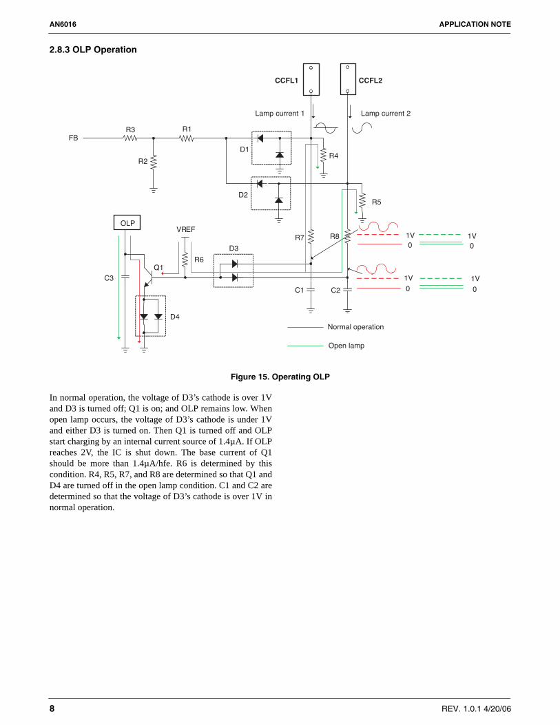
Figure 15. Operating OLP
In normal operation, the voltage of D3’s cathode is over 1Vand D3 is turned off; Q1 is on; and OLP remains low. Whenopen lamp occurs, the voltage of D3’s cathode is under 1Vand either D3 is turned on. Then Q1 is turned off and OLPstart charging by an internal current source of 1.4µA. If OLPreaches 2V, the IC is shut down. The base current of Q1should be more than 1.4µA/hfe. R6 is determined by thiscondition. R4, R5, R7, and R8 are determined so that Q1 andD4 are turned off in the open lamp condition. C1 and C2 aredetermined so that the voltage of D3’s cathode is over 1V innormal operation.
R2
R3
R6
C3
C1
D3
D1
Q1
D2
VREF
C2
CCFL1 CCFL2
Lamp current 1 Lamp current 2
D4
OLP
FB
0
0
1V
1V
R1
R4
R5
0
0
1V
1V
Normal operation
Open lamp
R7 R8

REV. 1.0.1 4/20/06 9
AN6016 APPLICATION NOTE
2.8.4 OLR Operation
Figure 16. Operating OLR
Figure 17. Open Lamp Regulation Circuit
Figure 18. Open Lamp Protection Circuit
Figure 19. OLR Voltage During Striking Mode
R2
R3
D1
D2
CCFL1
Lamp current 1
CCFL2
Lamp current 2
R1
R4
R5
OLR>2V
+
-
Error Amp. VREF
Solr
105μA OLR
-
+
2V
D3 D4
OLR > 2V ↑ → Solr on duty ↑ → EA_IN ↑ → EA_OUT ↑ → Switching duty ↑ → Lamp voltage ↓→ OLR > 2V ↓ → Solr on duty ↓ → EA_IN → EA_OUT ↓ → Switching duty ↑ → Lamp voltage ↑
OLR
-
+
2VSolr
105µA
To EA_IN
Q
Q SET
CLR
S
R UVLO
2.5V 1.5V
OLP
-
+
1.4µAUVLO
To Control Logic
VOLP
AN6016 APPLICATION NOTE
10 REV. 1.0.1 4/20/06
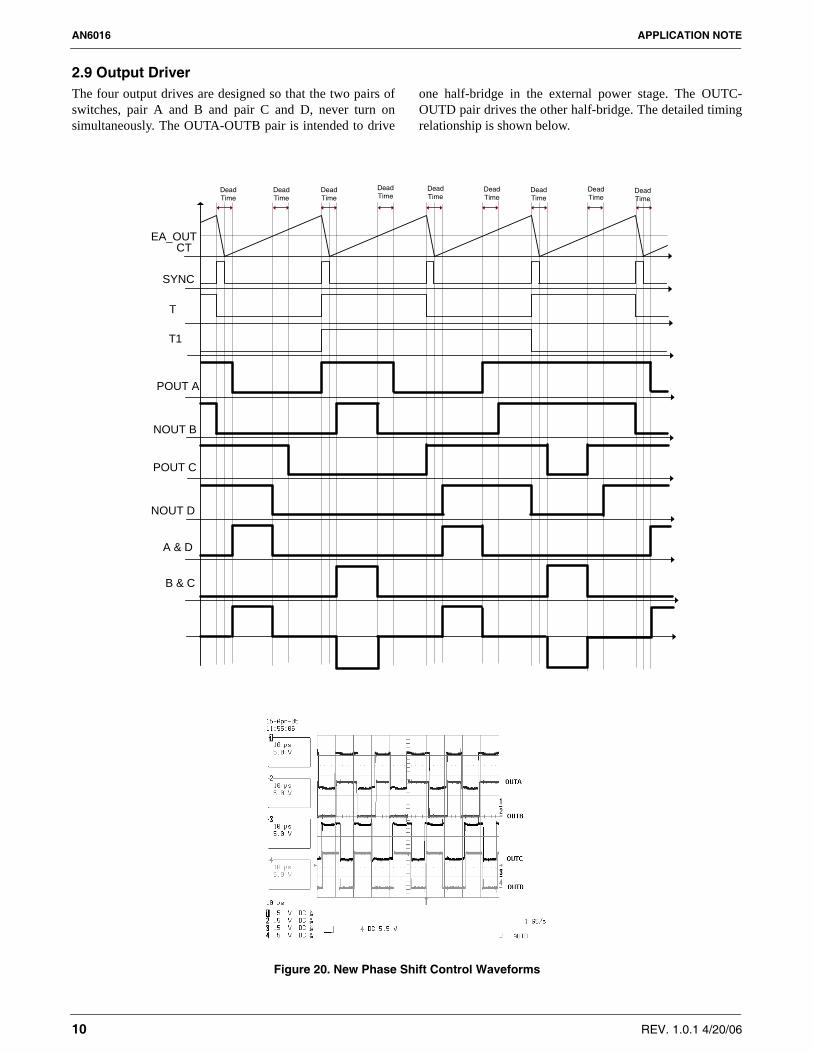
2.9 Output Driver The four output drives are designed so that the two pairs ofswitches, pair A and B and pair C and D, never turn onsimultaneously. The OUTA-OUTB pair is intended to drive
one half-bridge in the external power stage. The OUTC-OUTD pair drives the other half-bridge. The detailed timingrelationship is shown below.
Figure 20. New Phase Shift Control Waveforms
CT
SYNC
POUT A
NOUT B
POUT C
NOUT D
EA_OUT
A & D
B & C
T
T1
DeadTime
DeadTime
DeadTime
DeadTime
DeadTime
DeadTime
DeadTime
DeadTime
DeadTime

REV. 1.0.1 4/20/06 11
AN6016 APPLICATION NOTE
2.10 CCFL Striking Sequence
Figure 21. CCFL Ignites
Figure 22. CCFL Does Not Ignite
Figure 23. Open Lamp
ENA
OLP
S_S
RT1
Striking frequency Normal operation frequency
( ) TT1Tst CRR
F =//
16419
( ) TT1Tnor CRR
F =//
16419
0.5V
1V0.6V
..
..
ENA
OLP
S_S
RT1
Striking frequency
0.5V
1V
shutdown
2.5V
( ) TT1Tst CRR
F =//
16419
.
ENA
OLP
S_S
RT1
Open lamp
1.5V
( ) TT1Tnor CRR
F =//
16419
shutdown
4V
Normal
..

AN6016 APPLICATION NOTE
12 REV. 1.0.1 4/20/06
2.11 PCB Layout Guideline 1. Separating ground for analog and power portions of cir-
cuitry is one of the simplest and most effective methodsof noise suppression. This is shown in Figure 24.
2. The traces between drive output and the MOSFET gates should be as short as possible and as wide as possible.
3. The traces of RT, CT, and BCT should be kept away from high-current components and traces.
Figure 24. PCB Layout
OLP
OLR
ENA
S_S
GND
REF
ADIM
BDIM
EA_IN
EA_OUT
RT1
OUTB
OUTA
VIN
PGND
OUTC
OUTD
CT
RT
BCT
AGND
PGND
FAN7311

REV. 1.0.1 4/20/06 13
AN6016 APPLICATION NOTE
3. Power Stage Design
3.1 Resonant Circuit
Figure 25. Resonant Circuit
CpLM
Ll1 Ll2Cc
Ideal
Cpn2*LM
n2*L l1 Ll2Cc/n2 Ns/Np=n
R lamp
R lamp
R lamp
R lamp
Vrms
nVrms
Cp
n2*L l1 L l2Cc /n2
nVrms
nVrms
nVrms
nVrms
Cp
LlCc /n2
Cp
Ll
CsLl
Rs
(b)
(c)
(d)
(e)
(f)
(g)
Ideal transformer is neglected.
Assuming LM is infinite, IM is near zero.LM is neglected.
Primary and secondary side leakageinductances are combined.
DC blocking capacitor is neglected.
Transform the parallel resonant circuitinto the series resonant circuit.
Z
Z
CpLM
Ll1 Ll2Cc Np:Ns
Np:Ns
CCFL
Ideal
(a)
A circuit of LCD backlight inverter
CCFL A circuit of LCD backlight inverter
0
-VIN
VIN
V
INrms VπV 22=

AN6016 APPLICATION NOTE
14 REV. 1.0.1 4/20/06
The resonant circuit (f) in Fig. 25 is a second-order low-passfilter and can be described by the following normalizedparameters:
• The corner frequency:
• The characteristic impedance:
• The loaded quality factor at the corner frequency fo:
• The resonant frequency that forms the boundary between capacitive and inductive loads:
• The loaded quality factor at the resonant frequency fr:
• The input impedance of the resonant circuit (f) in Fig. 25is:
• The resonant frequency, fr, is defined as a frequency atwhich the phase shift is zero. The ratio of fr to the cornerfrequency, fo, is:
The loaded quality factors QL and Qr are related by:
3.2 Voltage Transfer Function
Figure 26. Input Voltage of the Resonant Circuit
As shown in Fig. 26, the input voltage of the resonant circuit v is a square wave of magnitude VIN, given by:
The fundamental component of this voltage is:
in which the amplitude of vi1 can be found from Fourieranalysis as:
You can obtain the rms value of vi1:
Which leads to the voltage transfer function from VIN to thefundamental component at the input of the resonant circuit:
ω01
LICp----------------= (3.1)
Z0 ω0LI1
ω0Cp-------------
LICp------= = = (3.2)
QL ω0CpRlampRlampω0LI--------------
RlampZ0
--------------= = = (3.3)
ωr1
LICs----------------= (3.4)
QrωrLIRs
----------- 1ωrCsRs------------------= = (3.5)
Z jωLRlamp
1jωCp-------------⋅
Rlamp1
jωCp-------------+
----------------------------------+Rlamp 1 ω
ω0------⎝ ⎠
⎛ ⎞ 2– j 1
QL------- ω
ω0------⎝ ⎠
⎛ ⎞+
1 jQLωω0------⎝ ⎠
⎛ ⎞+------------------------------------------------------------------------= =
Zejϕ RS jXs+= = (3.6)
ZZ0------
QL2 1 ω
ω0------⎝ ⎠
⎛ ⎞ 2–
2 ωω0------⎝ ⎠
⎛ ⎞ 2+
1 QLωω0------⎝ ⎠
⎛ ⎞ 2+
--------------------------------------------------------------= (3.7)
where,
ϕ arc QLωω0------⎝ ⎠
⎛ ⎞ ωω0------⎝ ⎠
⎛ ⎞ 2 1QL
2--------- 1–+⎩ ⎭⎨ ⎬⎧ ⎫
tan= (3.8)
RS Z ϕcos= (3.9)
XS Z ϕsin= (3.10)
frf0---- 1 1
QL2---------– , for QL ≥ 1= (3.11)
QrωrLRs
--------- 1ωrCsRs------------------ ωrCpRlamp= = =
Qr
ωρ
ω0−−−−⎝ ⎠
⎛ ⎞ QL2
1– , for QL ≥ 1= = (3.12)
v(t)
VIN
-VIN
2
23
2π
Dπ
π π
π
π
2
D2ωt
v 0, for 0 ωt 12--- D–⎝ ⎠
⎛ ⎞ π≤<=
v VIN, for 12--- D–⎝ ⎠
⎛ ⎞ π ωt 12--- D–⎝ ⎠
⎛ ⎞ π≤<=
v 0, for 12--- D+⎝ ⎠
⎛ ⎞ π ωt 32--- D–⎝ ⎠
⎛ ⎞ π≤<= (3.13)
v V– IN, for 32--- D–⎝ ⎠
⎛ ⎞ π ωt 32--- D–⎝ ⎠
⎛ ⎞ π≤<=
v 0, for 32--- D–⎝ ⎠
⎛ ⎞ π ωt 2π≤<=
vi1 Vm ωt( ) ,sin= (3.14)
Vm4π---VIN sin Dπ= (3.15)
VrmsVm
2-------- 2 2
π---------- VIN sin Dπ= = (3.16)
MVsVrmsVIN------------ 2 2
π---------- sin Dπ= = (3.17)

REV. 1.0.1 4/20/06 15
AN6016 APPLICATION NOTE
According to Fig. 25(f), the voltage transfer function of theresonant circuit is:
where,
The maximum value of MVr is obtained by differentiatingthe quantity under the square-root sign with respect to f/foand setting the result equal to zero. Hence, the normalizedpeak frequency is:
resulting in the maximum magnitude of the voltage transferfunction of the resonant circuit:
The magnitude of the DC-to-AC voltage transfer function ofthe LCD backlight inverter without losses is obtained from(3.17) and (3.22):
The maximum magnitude of the DC-to-AC voltage transferfunction of the LCD backlight inverter without losses is:
3.2 Design Procedure A LCD monitor backlight circuit illustrates a design basedon the FAN7311. The inverter is designed to drive twoCCFLs with the following specifications.
1) Select Transformer’s Primary Turns
The number of primary turns is determined by Faraday’slaw. Np,min is fixed by the minimum voltage across the pri-mary and the maximum on time.
where Np,min = Minimum number of primary turnsVIN,min = Minimum input voltage (Volts)
ΔB = Core magnetic flux density change (Tesla) Δtmax = Maximum overlap on-time of diagonal
MOSFET switches (us)Ae = Core cross-sectional area (mm2)
A transformer used in a full-bridge topology operates in twoquadrants of the B-H curve such that the maximum magneticflux density is Bmax = 0.5ΔB. For most cores, saturationmagnetic flux density is about 400mT. Margin considered,determine that the maximum magnetic flux density Bmax =0.5 Bsat, so the maximum magnetic flux density is Bmax =200mT. In an example with a minimum voltage of 9V, oper-ating frequency 50KHz, maximum on time of diagonalMOSFET switches of 10µs and a core cross-sectional area(EPC17, EPC19, EFD1820) of 22mm2, the minimum num-ber of primary turns required is:
MVrVRi
2 nVrms⋅---------------------------
RlampjωCp--------------
Rlamp1
jωCp-------------+
----------------------------------
jωL
RlampjωCp--------------
Rlamp1
jωCp-------------+
----------------------------------+
---------------------------------------------------= =
1
1 ωω0------⎝ ⎠
⎛ ⎞ 2– j 1
QL------- ω
ω0------⎝ ⎠
⎛ ⎞+---------------------------------------------------- MVr
ejϕ= = (3.18)
MVrVRi
nVrms--------------- 1
1 ωω0------⎝ ⎠
⎛ ⎞ 2–
2 1QL
2--------- ωω0------⎝ ⎠
⎛ ⎞ 2+
------------------------------------------------------------------= = (3.19)
ϕ -arctan
1QL------- ω
ω0------⎝ ⎠
⎛ ⎞
1 ωω0------⎝ ⎠
⎛ ⎞ 2–
-----------------------= (3.20)
fpkf0------- 0 for 0 QL
12
-------≤ ≤,= (3.21)
fpkf0------- 1 1
4QL2------------– for QL
12
-------≤,=
MVr max( ) 1 for 0 QL12
-------≤ ≤,=
MVr max( )QL
1 14QL
2------------–------------------------- , for QL
12
-------≤= (3.22)
MVIVlampVIN
-------------- MVs nMVr( )⋅= =
2 2 n sinDπ⋅
π 1 ωω0------⎝ ⎠
⎛ ⎞ 2– 1
QL2--------- ω
ω0------⎝ ⎠
⎛ ⎞ 2+
--------------------------------------------------------------------= (3.23)
Panel Model LM151X2(LG.PHILIPS LCD)
Input Voltage 9 ~ 15V
Striking Voltage 880Vrms
Operating Voltage 585Vrms (Typ.)
Operating Current 8mArms (Typ.)
Operating Frequency 50kHz (Typ.)
Rated Power 4.68W/CCFL
Efficiency 85% (Typ.)
MVl max( )2 2 n ⋅
π------------------- , for 0 QL
12
-------≤ ≤=
MVl max( )2 2 nQL⋅
π 1 14QL
2------------–----------------------------- , for QL ≥ 1
2-------= (3.24)
Np min,VIN min, Δtmax⋅
ΔB Ae⋅--------------------------------------=
Np min,VIN min, Δtmax⋅
ΔB Ae⋅-------------------------------------- 9 10⋅
400 22⋅------------------- 10Ts≈= =
AN6016 APPLICATION NOTE
16 REV. 1.0.1 4/20/06
2) Select QL and Operation Frequency to Determine the Turns Ratio
Select a value of 1 for QL. Assume that fop = fpk = 50kHzbased on the LCD panel specification. From (3.21), the cor-ner frequency is:
From (3.11), the resonant frequency that forms the boundarybetween capacitive and inductive loads is:
Therefore, zero-voltage switching (ZVS) can be achieved atany operating frequency. For the reference design, therequired secondary lamp voltage is 585V and the minimumvoltage is 9V. Therefore, from (3.23), the minimum numberof the turns ratio is:
3) Determine the Required Output Capacitance
Using the above specifications, the equivalent resistance of aCCFL is:
The corner frequency is 70.7kHz. Assume a parasitic capaci-tance per lamp of 10pF. Each parasitic capacitance is effec-tively in parallel with each of the output capacitors.
The output capacitor is:
Using (3.3), the value of the leakage inductance is:
Note: Considering minimum primary turns, minimum turnsratio, and leakage inductance, determine primary turns, turnsratio, and the gap of core to get the required leakage induc-tance. For the sample design, the number of primary turns is30Ts and that of the secondary turns is 2200Ts. Turns ratio is66.7.
4) Select the Proper Wire Gauges for the Primary andSecondary Transformer Windings
The approximate primary winding rms current Ip andapproximate secondary winding rms current Is are deter-mined by the following equations.
fofpk
1 12QL
2------------–------------------------- 50
1 12 1.12⋅-----------------–
------------------------------ 70.7 kHz( )= = =
fr fo 1 1QL
2---------–⋅ fpk
1 1QL
2---------–
1 12QL
2------------–-------------------------⋅ 0 kHz( )= = =
n 5859---------
π 1ωopω0---------⎝ ⎠
⎛ ⎞2
–2 1
QL2---------
ωopω0---------⎝ ⎠
⎛ ⎞2
+
2 2 sin Dπ---------------------------------------------------------------------------⋅≥ 62.5Ts, ≈
MVI∴ 2 2 n sin Dπ⋅
π 1 ωω0------⎝ ⎠
⎛ ⎞ 2–
2 1QL
2--------- ωω0------⎝ ⎠
⎛ ⎞ 2+
---------------------------------------------------------------------- 5859
---------≥=
RlampVlampIlamp-------------- 585
0.008------------- 75 kΩ( )≈= =
Cout Cp Cpara–QL
ωoRlamp--------------------- 10pF– 21pF,≈= =
QL∴ ωoRlampCp=
LI1
ωo2Cp
--------------- 164.6 mH( )≈=
Ipπ
2 2----------
PlampηVIN------------- ,⋅=
Plamp∴ ηVINIIN, IIN2 2
π----------Ip= =
Is Ilamp2 2πfopCoutVlamp[ ]+
2=

REV. 1.0.1 4/20/06 17
AN6016 APPLICATION NOTE
Values that must be known or selected initially:
Values that are calculated:
Values that must be selected with more than minimum turn ratio.
The values that are calculated:
Parameter Description Typical Value Units
Vlamp Nominal lamp operating voltage 585 V
Ilamp Nominal lamp operating current 8 mA
fop Operating frequency 50 kHz
fpk Peak frequency 50 kHz
Vin Input voltage 9 V
D Duty ratio at input voltage 50 %
QL Loaded factor at the corner frequency 1
Cpara Parasitic capacitance 10 pF
Ae Core cross-sectional area 22 mm2
Bsat Saturation magnetic flux density 0.4 T
ALleakage AL value of leakage inductance 22 nH/N2
Bmax Maximum magnetic flux density 0.2 T
ΔB Core magnetic flux density change 0.4 T
Δtmax Maximum overlap on-time of diagonal switches 10 µs
fo Corner frequency 70.71067812 kHz
fr Resonant frequency 0 kHz
Rlamp Equivalent resistance of a CCFL 73.125 k¾
Np,min The minimum number of transformer’s primary turns 10 Turns
nmin The minimum number of the turns ratio 62.5
Cout The output capacitor 20.78 pF
Ll The leakage inductance of the transformer 164.59 mH
Np The number of transformer’s primary turns 31 Turns
n The number of the turns ratio 62.5
Ns The number of transformer’s secondary turns 1934.1 Turns

4/20/06 0.0m 001© 2006 Fairchild Semiconductor Corporation
AN6016 APPLICATION NOTE
DISCLAIMER FAIRCHILD SEMICONDUCTOR RESERVES THE RIGHT TO MAKE CHANGES WITHOUT FURTHER NOTICE TO ANYPRODUCTS HEREIN TO IMPROVE RELIABILITY, FUNCTION, OR DESIGN. FAIRCHILD DOES NOT ASSUME ANY LIABILITY ARISING OUT OF THE APPLICATION OR USE OF ANY PRODUCT OR CIRCUIT DESCRIBED HEREIN; NEITHERDOES IT CONVEY ANY LICENSE UNDER ITS PATENT RIGHTS, NOR THE RIGHTS OF OTHERS. THESESPECIFICATIONS DO NOT EXPAND THE TERMS OF FAIRCHILD’S WORLDWIDE TERMS AND CONDITIONS,SPECIFICALLY THE WARRANTY THEREIN, WHICH COVERS THESE PRODUCTS.
LIFE SUPPORT POLICY
FAIRCHILD’S PRODUCTS ARE NOT AUTHORIZED FOR USE AS CRITICAL COMPONENTS IN LIFE SUPPORT DE-VICES OR SYSTEMS WITHOUT THE EXPRESS WRITTEN APPROVAL OF THE PRESIDENT OF FAIRCHILD SEMI-CONDUCTOR CORPORATION. As used herein:1. Life support devices or systems are devices or systems
which, (a) are intended for surgical implant into the body, or (b) support or sustain life, or (c) whose failure to perform when properly used in accordance with instructions for use provided in the labeling, can be reasonably expected to result in significant injury to the user.
2. A critical component is any component of a life support.
www.fairchildsemi.com
www.onsemi.com1
ON Semiconductor and are trademarks of Semiconductor Components Industries, LLC dba ON Semiconductor or its subsidiaries in the United States and/or other countries.ON Semiconductor owns the rights to a number of patents, trademarks, copyrights, trade secrets, and other intellectual property. A listing of ON Semiconductor’s product/patentcoverage may be accessed at www.onsemi.com/site/pdf/Patent−Marking.pdf. ON Semiconductor reserves the right to make changes without further notice to any products herein.ON Semiconductor makes no warranty, representation or guarantee regarding the suitability of its products for any particular purpose, nor does ON Semiconductor assume any liabilityarising out of the application or use of any product or circuit, and specifically disclaims any and all liability, including without limitation special, consequential or incidental damages.Buyer is responsible for its products and applications using ON Semiconductor products, including compliance with all laws, regulations and safety requirements or standards,regardless of any support or applications information provided by ON Semiconductor. “Typical” parameters which may be provided in ON Semiconductor data sheets and/orspecifications can and do vary in different applications and actual performance may vary over time. All operating parameters, including “Typicals” must be validated for each customerapplication by customer’s technical experts. ON Semiconductor does not convey any license under its patent rights nor the rights of others. ON Semiconductor products are notdesigned, intended, or authorized for use as a critical component in life support systems or any FDA Class 3 medical devices or medical devices with a same or similar classificationin a foreign jurisdiction or any devices intended for implantation in the human body. Should Buyer purchase or use ON Semiconductor products for any such unintended or unauthorizedapplication, Buyer shall indemnify and hold ON Semiconductor and its officers, employees, subsidiaries, affiliates, and distributors harmless against all claims, costs, damages, andexpenses, and reasonable attorney fees arising out of, directly or indirectly, any claim of personal injury or death associated with such unintended or unauthorized use, even if suchclaim alleges that ON Semiconductor was negligent regarding the design or manufacture of the part. ON Semiconductor is an Equal Opportunity/Affirmative Action Employer. Thisliterature is subject to all applicable copyright laws and is not for resale in any manner.
PUBLICATION ORDERING INFORMATIONN. American Technical Support: 800−282−9855 Toll FreeUSA/Canada
Europe, Middle East and Africa Technical Support:Phone: 421 33 790 2910
Japan Customer Focus CenterPhone: 81−3−5817−1050
www.onsemi.com
LITERATURE FULFILLMENT:Literature Distribution Center for ON Semiconductor19521 E. 32nd Pkwy, Aurora, Colorado 80011 USAPhone: 303−675−2175 or 800−344−3860 Toll Free USA/CanadaFax: 303−675−2176 or 800−344−3867 Toll Free USA/CanadaEmail: [email protected]
ON Semiconductor Website: www.onsemi.com
Order Literature: http://www.onsemi.com/orderlit
For additional information, please contact your localSales Representative
© Semiconductor Components Industries, LLC