Embed Size (px)
Citation preview

To learn more about ON Semiconductor, please visit our website at www.onsemi.com
Please note: As part of the Fairchild Semiconductor integration, some of the Fairchild orderable part numbers will need to change in order to meet ON Semiconductor’s system requirements. Since the ON Semiconductor product management systems do not have the ability to manage part nomenclature that utilizes an underscore (_), the underscore (_) in the Fairchild part numbers will be changed to a dash (-). This document may contain device numbers with an underscore (_). Please check the ON Semiconductor website to verify the updated device numbers. The most current and up-to-date ordering information can be found at www.onsemi.com. Please email any questions regarding the system integration to [email protected].
Is Now Part of
ON Semiconductor and the ON Semiconductor logo are trademarks of Semiconductor Components Industries, LLC dba ON Semiconductor or its subsidiaries in the United States and/or other countries. ON Semiconductor owns the rights to a number of patents, trademarks, copyrights, trade secrets, and other intellectual property. A listing of ON Semiconductor’s product/patent coverage may be accessed at www.onsemi.com/site/pdf/Patent-Marking.pdf. ON Semiconductor reserves the right to make changes without further notice to any products herein. ON Semiconductor makes no warranty, representation or guarantee regarding the suitability of its products for any particular purpose, nor does ON Semiconductor assume any liability arising out of the application or use of any product or circuit, and specifically disclaims any and all liability, including without limitation special, consequential or incidental damages. Buyer is responsible for its products and applications using ON Semiconductor products, including compliance with all laws, regulations and safety requirements or standards, regardless of any support or applications information provided by ON Semiconductor. “Typical” parameters which may be provided in ON Semiconductor data sheets and/or specifications can and do vary in different applications and actual performance may vary over time. All operating parameters, including “Typicals” must be validated for each customer application by customer’s technical experts. ON Semiconductor does not convey any license under its patent rights nor the rights of others. ON Semiconductor products are not designed, intended, or authorized for use as a critical component in life support systems or any FDA Class 3 medical devices or medical devices with a same or similar classification in a foreign jurisdiction or any devices intended for implantation in the human body. Should Buyer purchase or use ON Semiconductor products for any such unintended or unauthorized application, Buyer shall indemnify and hold ON Semiconductor and its officers, employees, subsidiaries, affiliates, and distributors harmless against all claims, costs, damages, and expenses, and reasonable attorney fees arising out of, directly or indirectly, any claim of personal injury or death associated with such unintended or unauthorized use, even if such claim alleges that ON Semiconductor was negligent regarding the design or manufacture of the part. ON Semiconductor is an Equal Opportunity/Affirmative Action Employer. This literature is subject to all applicable copyright laws and is not for resale in any manner.

© 2008 Fairchild Semiconductor Corporation www.fairchildsemi.com
FAN
7371 � H
igh-Current H
igh-Side Gate D
rive IC
FAN7371 Rev. 1.0.2
November 2009
FAN7371High-Current High-Side Gate Drive ICFeatures! Floating Channel for Bootstrap Operation to +600V! 4A/4A Sourcing/Sinking Current Driving Capability! Common-Mode dv/dt Noise Canceling Circuit! 3.3V and 5V Input Logic Compatible! Output In-phase with Input Signal! Under- Voltage Lockout for VBS! 25V Shunt Regulator on VDD and VBS! 8-Lead Small Outline Package (SOP)
Applications! High-Speed Gate Driver ! Sustaine Switch Driver in PDP Application! Energy-Recovery Circuit Switch Driver in
PDP Application! High-Power Buck Converter! Motor Drive Inverter
Description The FAN7371 is a monolithic high-side gate drive IC,which can drive high-speed MOSFETs and IGBTs thatoperate up to +600V. It has a buffered output stage withall NMOS transistors designed for high pulse currentdriving capability and minimum cross-conduction.
Fairchild�s high-voltage process and common-modenoise canceling techniques provide stable operation ofthe high-side driver under high dv/dt noise circum-stances. An advanced level-shift circuit offers high-sidegate driver operation up to VS=-9.8V (typical) forVBS=15V.
The UVLO circuit prevents malfunction when VBS islower than the specified threshold voltage.
The high-current and low-output voltage drop featuremakes this device suitable for sustaine switch driver andenergy recovery switch driver in the Plasma DisplayPanel application, motor drive inverter, switching powersupply, and high-power DC-DC converter applications.
Ordering Information
Note:1. These devices passed wave soldering test by JESD22A-111.
For Fairchild�s definition of Eco Status, please visit: http://www.fairchildsemi.com/company/green/rohs_green.html.
8-SOP
Part Number Package OperatingTemperature Range Eco Status Packing Method
FAN7371M(1)8-SOP -40°C ~ 125°C RoHS
Tube
FAN7371MX(1) Tape & Reel

FAN
7371 � H
igh-Current H
igh-Side Gate D
rive IC
© 2008 Fairchild Semiconductor Corporation www.fairchildsemi.comFAN7371 Rev. 1.0.2 2
Typical Application Diagrams
Figure 1. Floated Bidirectional Switch and Half-Bridge Driver: PDP application
Figure 2. Step-Down (Buck) DC-DC Converter Application
Energy Recovery Circuit Part Sustain Drive Part
DBOOT1
D2
C2
IN1
To PannelDBOOT2
CBOOT1
Q1
D1
D3
D4
L1
IN2
15V
Q2
RBOOT1
CBOOT2
VS DBOOT3
IN3Q3
RBOOT3
CBOOT3
15V
IN4Q4
R1
R2
R5
R6C1 C3R8
R7
R4
R3
FAN7371
VB
IN
GND
HO
VS
NC
1
2
NC
VDD
7
5
6
8
3
4
FAN7371
VB
IN
GND
HO
VS
NC
1
2
NC
VDD
7
5
6
8
3
4
FAN7371
VB
IN
GND
HO
VS
NC
1
2
NC
VDD
7
5
6
8
3
4
FAN7371
VB
IN
GND
HO
VS
NC
1
2
NC
VDD
7
5
6
8
3
4
FAN7371 Rev.03
DBOOT
C2
PWMCBOOT
C1
D1
L1
15V
RBOOT
R2
FAN7371VB
IN
GND
HO
VS
NC
NC
VDD
7
5
6
8
2
4
3
1
R1
VIN
VOUT
FAN7371 Rev.01
FAN
7371 � H
igh-Current H
igh-Side Gate D
rive IC
© 2008 Fairchild Semiconductor Corporation www.fairchildsemi.comFAN7371 Rev. 1.0.2 3
Internal Block Diagram
Figure 3. Functional Block Diagram
Pin Configuration
Figure 4. Pin Configuration (Top View)
Pin DefinitionsPin # Name Description
1 VDD Supply Voltage
2 IN Logic Input for High-Side Gate Driver Output
3 NC No Connection
4 GND Ground
5 NC No Connection
6 VS High-Voltage Floating Supply Return
7 HO High-Side Driver Output
8 VB High-Side Floating Supply
UVLO
PULSE
GEN
ERA
TOR
VDD
GND
IN
VB
HO
VS
RR
S Q
6
7
81
4
2 NOISECANCELLER
Pins 3 and 5 are no connection.
25V
FAN7371 Rev.04
25V110K
VDD
Shoo
t-thr
ough
cur
rent
co
mpe
nsat
ed g
ate
driv
erVS
VB
FAN7371
VDD
NC
IN HO
NC4GND
3
2
1
5
6
7
8
FAN7371 Rev.01
FAN
7371 � H
igh-Current H
igh-Side Gate D
rive IC
© 2008 Fairchild Semiconductor Corporation www.fairchildsemi.comFAN7371 Rev. 1.0.2 4
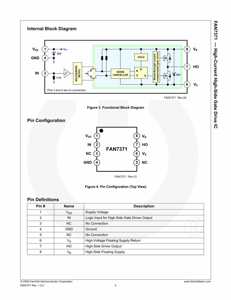
Absolute Maximum RatingsStresses exceeding the absolute maximum ratings may damage the device. The device may not function or be opera-ble above the recommended operating conditions and stressing the parts to these levels is not recommended. In addi-tion, extended exposure to stresses above the recommended operating conditions may affect device reliability. Theabsolute maximum ratings are stress ratings only. TA=25°C unless otherwise specified.
Notes: 2 This IC contains a shunt regulator on VDD and VBS with a normal breakdown voltage of 25V. Please note that this
supply pin should not be driven by a low-impedance voltage source greater than the VSHUNT specified in theElectrical Characteristics section
3 Mounted on 76.2 x 114.3 x 1.6mm PCB (FR-4 glass epoxy material).4 Refer to the following standards:
JESD51-2: Integral circuits thermal test method environmental conditions, natural convection, andJESD51-3: Low effective thermal conductivity test board for leaded surface mount packages.
5 Do not exceed power dissipation (PD) under any circumstances.
Recommended Operating ConditionsThe Recommended Operating Conditions table defines the conditions for actual device operation. Recommendedoperating conditions are specified to ensure optimal performance to the datasheet specifications. Fairchild does notrecommend exceeding them or designing to absolute maximum ratings.
Symbol Characteristics Min. Max. UnitVS High-Side Floating Offset Voltage VB-VSHUNT VB+0.3 V
VB High-Side Floating Supply Voltage(2) -0.3 625.0 V
VHO High-Side Floating Output Voltage VS-0.3 VB+0.3 V
VDD Low-Side and Logic Supply Voltage(2) -0.3 VSHUNT V
VIN Logic Input Voltage -0.3 VDD+0.3 V
dVS/dt Allowable Offset Voltage Slew Rate ± 50 V/ns
PD Power Dissipation(3, 4, 5) 0.625 W
θJA Thermal Resistance 200 °C/W
TJ Junction Temperature -55 +150 °C
TSTG Storage Temperature -55 +150 °C
TA Operating Ambient Temperature -40 +125 °C
Symbol Parameter Min. Max. UnitVBS High-Side Floating Supply Voltage VS+10 VS+20 V
VS High-Side Floating Supply Offset Voltage 6-VDD 600 V
VHO High-Side Output Voltage VS VB V
VIN Logic Input Voltage GND VDD V
VDD Supply Voltage 10 20 V

FAN
7371 � H
igh-Current H
igh-Side Gate D
rive IC
© 2008 Fairchild Semiconductor Corporation www.fairchildsemi.comFAN7371 Rev. 1.0.2 5
Electrical Characteristics VBIAS(VDD, VBS)=15.0V, TA = 25°C, unless otherwise specified. The VIN and IIN parameters are referenced to GND.The VO and IO parameters are relative to VS and are applicable to the respective output HO.
Note: 6 These parameters guaranteed by design.
Dynamic Electrical Characteristics VDD=VBS=15V, GND=0V, CLOAD=1000pF, TA=25°C, unless otherwise specified.
.
Symbol Characteristics Test Condition Min. Typ. Max. UnitPOWER SUPPLY SECTION
IQDD Quiescent VDD Supply Current VIN=0V or 5V 25 70 μAIPDD Operating VDD Supply Current fIN=20KHz, No Load 35 100 μA
BOOTSTRAPPED SUPPLY SECTION
VBSUV+VBS Supply Under-Voltage Positive Going Threshold Voltage
VBS=Sweep 8.2 9.2 10.2 V
VBSUV-VBS Supply Under-Voltage Negative Going Threshold Voltage
VBS=Sweep 7.5 8.5 9.5 V
VBSHYSVBS Supply Under-Voltage Lockout Hysteresis Voltage
VBS=Sweep 0.7 V
ILK Offset Supply Leakage Current VB=VS=600V 10 μAIQBS Quiescent VBS Supply Current VIN=0V or 5V 60 120 μA
IPBS Operating VBS Supply Current CLOAD=1nF, fIN=20KHz, rms Value 1.0 2.8 mA
SHUNT REGULATOR SECTION
VSHUNTVDD and VBS Shunt Regulator Clamping Voltage
ISHUNT=5mA 24 25 V
INPUT LOGIC SECTIONVIH Logic �1� Input Voltage 2.5 VVIL Logic �0� Input Voltage 0.8 VIIN+ Logic Input High Bias Current VIN=5V 45 70 μAIIN- Logic Input Low Bias Current VIN=0V 2 μARIN Input Pull-down Resistance 70 110 KΩ
GATE DRIVER OUTPUT SECTIONVOH High Level Output Voltage (VBIAS - VO) No Load 1.2 VVOL Low Level Output Voltage No Load 30 mVIO+ Output High, Short-Circuit Pulsed Current(6) VHO=0V, VIN=5V, PW ≤10µs 3.0 4.0 AIO- Output Low, Short-Circuit Pulsed Current(6) VHO=15V,VIN=0V, PW ≤10µs 3.0 4.0 A
VSAllowable Negative VS pin Voltage for IN Signal Propagation to HO -9.8 -7.0 V
Symbol Parameter Conditions Min. Typ. Max. Unitton Turn-on Propagation Delay Time VS=0V 150 210 ns
toff Turn-off Propagation Delay Time VS=0V 150 210 ns
tr Turn-on Rise Time 25 50 ns
tf Turn-off Fall Time 15 40 ns
FAN
7371 � H
igh-Current H
igh-Side Gate D
rive IC
© 2008 Fairchild Semiconductor Corporation www.fairchildsemi.comFAN7371 Rev. 1.0.2 6
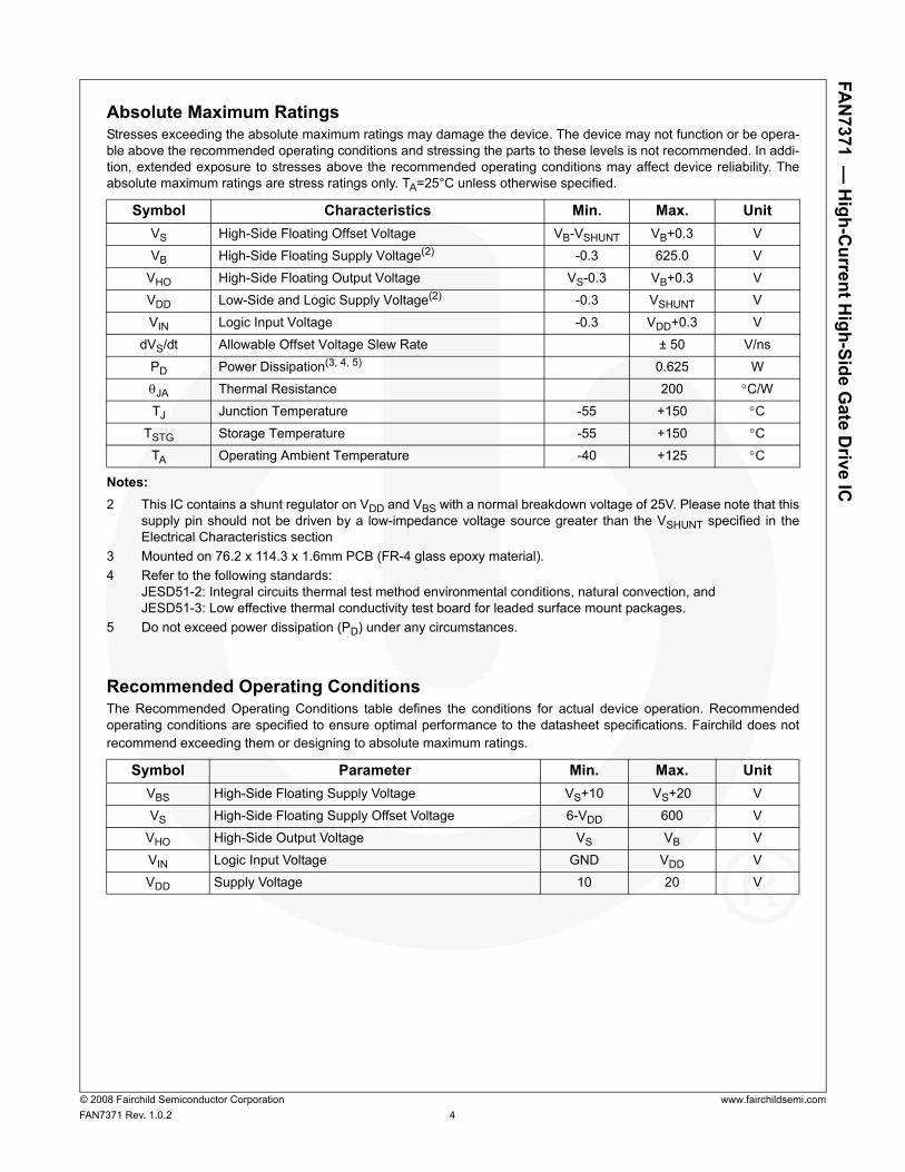
Typical Characteristics
Figure 5. Turn-on Propagation Delay vs. Temperature
Figure 6. Turn-off Propagation Delay vs. Temperature
Figure 7. Turn-on Rise Time vs. Temperature Figure 8. Turn-off Fall Time vs. Temperature
Figure 9. Operating VDD Supply Current
vs. Temperature
Figure 10. Operating VBS Supply Current
vs. Temperature
-40 -20 0 20 40 60 80 100 1200
50
100
150
200
250
t ON [n
s]
Temperature [°C]-40 -20 0 20 40 60 80 100 1200
50
100
150
200
250
t OFF
[ns]
Temperature [°C]
-40 -20 0 20 40 60 80 100 1200
10
20
30
40
50
t R [n
s]
Temperature [°C]-40 -20 0 20 40 60 80 100 1200
10
20
30
40
50
t F [n
s]
Temperature [°C]
-40 -20 0 20 40 60 80 100 1200
20
40
60
80
100
I PD
D [μ
A]
Temperature [°C]-40 -20 0 20 40 60 80 100 120
0.0
0.5
1.0
1.5
2.0
I PBS
[mA]
Temperature [°C]

FAN
7371 � H
igh-Current H
igh-Side Gate D
rive IC
© 2008 Fairchild Semiconductor Corporation www.fairchildsemi.comFAN7371 Rev. 1.0.2 7
Typical Characteristics (Continued)
Figure 11. VBS UVLO+ vs. Temperature Figure 12. VBS UVLO- vs. Temperature
Figure 13. Logic High Input Voltage vs. Temperature Figure 14. Logic Low Input Voltage vs. Temperature
Figure 15. Input Pull-Down Resistance vs.Temperature.
Figure 16. High-Level Output Voltage vs. Temperature
-40 -20 0 20 40 60 80 100 1208.0
8.5
9.0
9.5
10.0
VBS
UV
+ [V]
Temperature [°C]
-40 -20 0 20 40 60 80 100 1207.5
8.0
8.5
9.0
9.5
V BS
UV
- [V]
Temperature [°C]
-40 -20 0 20 40 60 80 100 1200.0
0.5
1.0
1.5
2.0
2.5
3.0
VIH
[V]
Temperature [°C]-40 -20 0 20 40 60 80 100 120
0.0
0.5
1.0
1.5
2.0
2.5
3.0
V IL
[V]
Temperature [°C]
-40 -20 0 20 40 60 80 100 1200
40
80
120
160
200
240
280
RIN
[kΩ
]
Temperature [°C]-40 -20 0 20 40 60 80 100 120
0.00
0.25
0.50
0.75
1.00
1.25
1.50
VO
H [V
]
Temperature [°C]
FAN
7371 � H
igh-Current H
igh-Side Gate D
rive IC
© 2008 Fairchild Semiconductor Corporation www.fairchildsemi.comFAN7371 Rev. 1.0.2 8
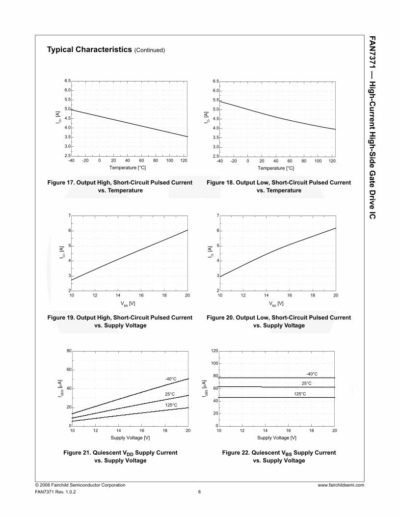
Typical Characteristics (Continued)
Figure 17. Output High, Short-Circuit Pulsed Current vs. Temperature
Figure 18. Output Low, Short-Circuit Pulsed Current vs. Temperature
Figure 19. Output High, Short-Circuit Pulsed Current vs. Supply Voltage
Figure 20. Output Low, Short-Circuit Pulsed Current vs. Supply Voltage
Figure 21. Quiescent VDD Supply Current vs. Supply Voltage
Figure 22. Quiescent VBS Supply Current vs. Supply Voltage
-40 -20 0 20 40 60 80 100 1202.5
3.0
3.5
4.0
4.5
5.0
5.5
6.0
6.5
I O+ [A
]
Temperature [°C]-40 -20 0 20 40 60 80 100 120
2.5
3.0
3.5
4.0
4.5
5.0
5.5
6.0
6.5
I O- [A
]
Temperature [°C]
10 12 14 16 18 202
3
4
5
6
7
I O+ [A
]
VBS [V]
10 12 14 16 18 202
3
4
5
6
7
I O
- [A]
VBS [V]
10 12 14 16 18 200
20
40
60
80
25°C
-40°C
I QD
D [μ
A]
Supply Voltage [V]
125°C
10 12 14 16 18 200
20
40
60
80
100
120
25°C
-40°C
I QB
S [μ
A]
Supply Voltage [V]
125°C
FAN
7371 � H
igh-Current H
igh-Side Gate D
rive IC
© 2008 Fairchild Semiconductor Corporation www.fairchildsemi.comFAN7371 Rev. 1.0.2 9
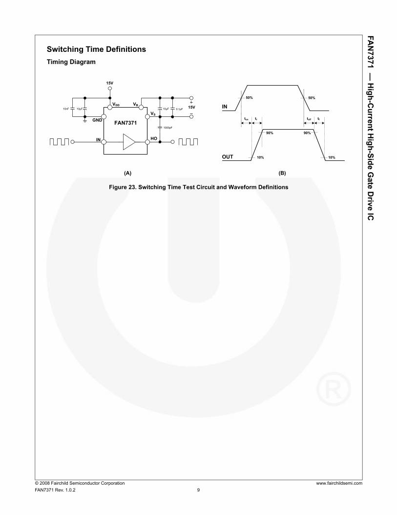
Switching Time DefinitionsTiming Diagram
Figure 23. Switching Time Test Circuit and Waveform Definitions
0.1µF
VB 15V
HO
10µF
1000pF
IN
OUT
50%
90%
50%
ton
10%
tr toff tf
10%
90%
FAN7371
(A) (B)
10nF
15V
10µFVDD
VS
GND
IN

FAN
7371 � H
igh-Current H
igh-Side Gate D
rive IC
© 2008 Fairchild Semiconductor Corporation www.fairchildsemi.comFAN7371 Rev. 1.0.2 10
Physical Dimensions
Figure 24. 8-Lead Small Outline Package (SOP)
Package drawings are provided as a service to customers considering Fairchild components. Drawings may change in any mannerwithout notice. Please note the revision and/or date on the drawing and contact a Fairchild Semiconductor representative to verify orobtain the most recent revision. Package specifications do not expand the terms of Fairchild�s worldwide terms and conditions, specifically the warranty therein, which covers Fairchild products.
Always visit Fairchild Semiconductor�s online packaging area for the most recent package drawings:http://www.fairchildsemi.com/packaging/.
8°0°
SEE DETAIL A
NOTES: UNLESS OTHERWISE SPECIFIED
A) THIS PACKAGE CONFORMS TO JEDEC MS-012, VARIATION AA, ISSUE C, B) ALL DIMENSIONS ARE IN MILLIMETERS. C) DIMENSIONS DO NOT INCLUDE MOLD FLASH OR BURRS. D) LANDPATTERN STANDARD: SOIC127P600X175-8M. E) DRAWING FILENAME: M08AREV13
LAND PATTERN RECOMMENDATION
SEATING PLANE
0.10 C
C
GAGE PLANE
x 45°
DETAIL ASCALE: 2:1
PIN ONEINDICATOR
4
8
1
CM B A0.25
B5
A
5.60
0.65
1.75
1.27
6.205.80
3.81
4.003.80
5.004.80
(0.33)1.27
0.510.33
0.250.10
1.75 MAX0.250.19
0.36
0.500.25R0.10
R0.10
0.900.406 (1.04)
OPTION A - BEVEL EDGE
OPTION B - NO BEVEL EDGE

FAN
7371 � H
igh-Current H
igh-Side Gate D
rive IC
© 2008 Fairchild Semiconductor Corporation www.fairchildsemi.comFAN7371 Rev. 1.0.2 12

www.onsemi.com1
ON Semiconductor and are trademarks of Semiconductor Components Industries, LLC dba ON Semiconductor or its subsidiaries in the United States and/or other countries.ON Semiconductor owns the rights to a number of patents, trademarks, copyrights, trade secrets, and other intellectual property. A listing of ON Semiconductor’s product/patentcoverage may be accessed at www.onsemi.com/site/pdf/Patent−Marking.pdf. ON Semiconductor reserves the right to make changes without further notice to any products herein.ON Semiconductor makes no warranty, representation or guarantee regarding the suitability of its products for any particular purpose, nor does ON Semiconductor assume any liabilityarising out of the application or use of any product or circuit, and specifically disclaims any and all liability, including without limitation special, consequential or incidental damages.Buyer is responsible for its products and applications using ON Semiconductor products, including compliance with all laws, regulations and safety requirements or standards,regardless of any support or applications information provided by ON Semiconductor. “Typical” parameters which may be provided in ON Semiconductor data sheets and/orspecifications can and do vary in different applications and actual performance may vary over time. All operating parameters, including “Typicals” must be validated for each customerapplication by customer’s technical experts. ON Semiconductor does not convey any license under its patent rights nor the rights of others. ON Semiconductor products are notdesigned, intended, or authorized for use as a critical component in life support systems or any FDA Class 3 medical devices or medical devices with a same or similar classificationin a foreign jurisdiction or any devices intended for implantation in the human body. Should Buyer purchase or use ON Semiconductor products for any such unintended or unauthorizedapplication, Buyer shall indemnify and hold ON Semiconductor and its officers, employees, subsidiaries, affiliates, and distributors harmless against all claims, costs, damages, andexpenses, and reasonable attorney fees arising out of, directly or indirectly, any claim of personal injury or death associated with such unintended or unauthorized use, even if suchclaim alleges that ON Semiconductor was negligent regarding the design or manufacture of the part. ON Semiconductor is an Equal Opportunity/Affirmative Action Employer. Thisliterature is subject to all applicable copyright laws and is not for resale in any manner.
PUBLICATION ORDERING INFORMATIONN. American Technical Support: 800−282−9855 Toll FreeUSA/Canada
Europe, Middle East and Africa Technical Support:Phone: 421 33 790 2910
Japan Customer Focus CenterPhone: 81−3−5817−1050
www.onsemi.com
LITERATURE FULFILLMENT:Literature Distribution Center for ON Semiconductor19521 E. 32nd Pkwy, Aurora, Colorado 80011 USAPhone: 303−675−2175 or 800−344−3860 Toll Free USA/CanadaFax: 303−675−2176 or 800−344−3867 Toll Free USA/CanadaEmail: [email protected]
ON Semiconductor Website: www.onsemi.com
Order Literature: http://www.onsemi.com/orderlit
For additional information, please contact your localSales Representative
© Semiconductor Components Industries, LLC
Mouser Electronics
Authorized Distributor
Click to View Pricing, Inventory, Delivery & Lifecycle Information: ON Semiconductor:
FAN7371MX FAN7371M