Embed Size (px)
Citation preview

DGD2101M Document number: DS39633 Rev. 1 - 2
1 of 11 www.diodes.com
April 2017 © Diodes Incorporated
DGD2101M
HIGH-SIDE AND LOW-SIDE GATE DRIVER IN SO-8 (Type TH)
Description
The DGD2101M is a high-voltage / high-speed gate driver capable of
driving N-Channel MOSFETs and IGBTs in a high-side/low-side
configuration. High-voltage processing techniques enable the
DGD2101M’s high side to switch to 600V in a bootstrap operation.
The 50ns (max) propagation delay matching between the high and the
low side drivers allows high frequency switching.
The DGD2101M logic inputs are compatible with standard TTL and
CMOS levels (down to 3.3V) for easy interfacing with controlling
devices. The driver outputs feature high-pulse current buffers
designed for minimum driver cross conduction. The low-side gate
driver and logic share a common ground.
The DGD2101M is available in a space saving 8-pin SO-8 (Type TH)
package, the operating temperature extends from -40°C to +125°C.
Applications
DC-DC Converters
DC-AC Inverters
AC-DC Power Supplies
Motor Controls
Class D Power Amplifiers
Features
Floating High-side Driver in Bootstrap Operation to 600V
Drives Two N-Channel MOSFETs or IGBTs in High-side / Low-
side Configuation
Outputs Tolerant to Negative Transients
Wide Low-side Gate Driver and Logic Supply: 10V to 20V
Logic Inputs CMOS and TTL Compatible (Down to 3.3V)
Schmitt Triggered Logic Inputs with Internal Pull Down
Undervoltage Lockout for VCC
Space Saving SO-8 (Type TH) Package Available
Extended Temperature Range: -40°C to +125°C
Totally Lead-Free & Fully RoHS Compliant (Notes 1 & 2)
Halogen and Antimony Free. “Green” Device (Note 3)
Mechanical Data
Case: SO-8 (Type TH)
Case Material: Molded Plastic. ―Green‖ Molding Compound; UL
Flammability Classification Rating 94V-0
Moisture Sensitivity: Level 3 per J-STD-020
Terminals: Finish – Matte Tin Plated Leads, Solderable per
MIL-STD-202, Method 208
SO-8 (Type TH) Weight: 0.075 grams (Approximate)
Ordering Information (Note 4)
Part Number Marking Reel Size (inches) Tape Width (mm) Quantity Per Reel
DGD2101MS8-13 DGD21012 13 12 2,500
Notes: 1. No purposely added lead. Fully EU Directive 2002/95/EC (RoHS) & 2011/65/EU (RoHS 2) compliant. 2. See http://www.diodes.com/quality/lead_free.html for more information about Diodes Incorporated’s definitions of Halogen- and Antimony-free, "Green" and Lead-free. 3. Halogen- and Antimony-free "Green‖ products are defined as those which contain <900ppm bromine, <900ppm chlorine (<1500ppm total Br + Cl) and <1000ppm antimony compounds. 4. For packaging details, go to our website at http://www.diodes.com/products/packages.html.
Marking Information
SO-8 (Type TH)
Top View Typical Configuration
DGD21012
YY WW
= Manufacturer’s Marking DGD21012 = Product Type Marking Code YY = Year (ex: 17 = 2017) WW = Week (01 to 53)

DGD2101M Document number: DS39633 Rev. 1 - 2
2 of 11 www.diodes.com
April 2017 © Diodes Incorporated
DGD2101M
Pin Diagrams
1
2
3
4
8
7
6
5
VCC
HIN
LIN
COM LO
VS
HO
VB
Pin Descriptions
Pin Number Pin Name Function
1 VCC Low-side and logic fixed supply
2 HIN Logic input for high-side gate driver output (HO), in phase
3 LIN Logic input for low-side gate driver output (LO), in phase
4 COM Low-side return
5 LO Low-side gate drive output
6 VS High-side floating supply return
7 HO High-side gate drive output
8 VB High-side floating supply
Functional Block Diagram
Top View: SO-8 (Type TH)

DGD2101M Document number: DS39633 Rev. 1 - 2
3 of 11 www.diodes.com
April 2017 © Diodes Incorporated
DGD2101M
Absolute Maximum Ratings (@TA = +25°C, unless otherwise specified.)
Characteristic Symbol Value Unit
High-Side Floating Supply Voltage VB -0.3 to +624 V
High-Side Floating Supply Offset Voltage VS VB-24 to VB+0.3 V
High-Side Floating Output Voltage VHO VS-0.3 to VB+0.3 V
Offset Supply Voltage Transient dVS / dt 50 V/ns
Low-Side and Logic Fixed Supply Voltage VCC -0.3 to +24 V
Low-Side Output Voltage VLO -0.3 to VCC+0.3 V
Logic Input Voltage (HIN and LIN) VIN -0.3 to VCC+0.3 V
Thermal Characteristics (@TA = +25°C, unless otherwise specified.)
Characteristic Symbol Value Unit
Power Dissipation Linear Derating Factor (Note 5) PD 0.625 W
Thermal Resistance, Junction to Ambient (Note 5) RθJA 200 °C/W
Thermal Resistance, Junction to Case (Note 5) RθJC 45 °C/W
Operating Temperature TJ +150 °C
Storage Temperature Range TSTG -55 to +150
Note: 5. When mounted on a standard JEDEC 2-layer FR-4 board.
Recommended Operating Conditions
Parameter Symbol Min Max Unit
High-Side Floating Supply Absolute Voltage VB VS + 10 VS + 20 V
High-Side Floating Supply Offset Voltage VS (Note 6) 600 V
High-Side Floating Output Voltage VHO VS VB V
Low-Side and Logic Fixed Supply Voltage VCC 10 20 V
Low-Side Output Voltage VLO 0 VCC V
Logic Input Voltage (HIN and LIN) VIN 0 5 V
Ambient Temperature TA -40 +125 °C
Note: 6. Logic operation for VS = -5V to +600V.

DGD2101M Document number: DS39633 Rev. 1 - 2
4 of 11 www.diodes.com
April 2017 © Diodes Incorporated
DGD2101M
DC Electrical Characteristics (VBIAS (VCC, VBS) = 15V, @TA = +25°C, unless otherwise specified.) (Note 7)
Parameter Symbol Min Typ Max Unit Conditions
Logic ―1‖ Input Voltage VIH 2.5 — — V VCC = 10V to 20V
Logic ―0‖ Input Voltage VIL — — 0.8 V VCC = 10V to 20V
High Level Output Voltage, VBIAS - VO VOH — 0.05 0.2 V IO = 2mA
Low Level Output Voltage, VO VOL — 0.02 0.1 V IO = 2mA
Offset Supply Leakage Current ILK — — 50 µA VB = VS = 600V
Quiescent VBS Supply Current IBSQ — 30 55 µA VIN = 0V or 5V
Quiescent VCC Supply Current ICCQ — 150 270 µA VIN = 0V or 5V
Logic ―1‖ Input Bias Current IIN+ — 3.0 10 µA VIN = 5V
Logic ―0‖ Input Bias Current IIN- — — 5.0 µA VIN = 0V
VCC Supply Undervoltage Positive Going Threshold VCCUV+ 8.0 8.9 9.8 V —
VCC Supply Undervoltage Negative Going Threshold VCCUV- 7.4 8.2 9.0 V —
Output High Short Circuit Pulsed Current IO+ 130 290 — mA VO = 0V, VIN = Logic―1‖, PW ≤ 10µs
Output Low Short Circuit Pulsed Current IO- 270 600 — mA VO = 15V, VIN = Logic―0‖, PW ≤ 10µs
Note: 7. The VIN and IIN parameters are referenced to COM. The VO and IO parameters are referenced to COM and are applicable to the respective output pins:
HO and LO.
AC Electrical Characteristics (VBIAS (VCC, VBS) = 15V, CL = 1000pF, @TA = +25°C, unless otherwise specified.)
Parameter Symbol Min Typ Max Unit Conditions
Turn-on Propagation Delay tON — 160 220 ns VS = 0V
Turn-off Propagation Delay tOFF — 150 220 ns VS = 600V
Turn-on Rise Time tR — 70 170 ns —
Turn-off Fall Time tF — 35 90 ns —
Delay Matching tDM — — 50 ns —

DGD2101M Document number: DS39633 Rev. 1 - 2
5 of 11 www.diodes.com
April 2017 © Diodes Incorporated
DGD2101M
Timing Waveforms
tF tR

DGD2101M Document number: DS39633 Rev. 1 - 2
6 of 11 www.diodes.com
April 2017 © Diodes Incorporated
DGD2101M
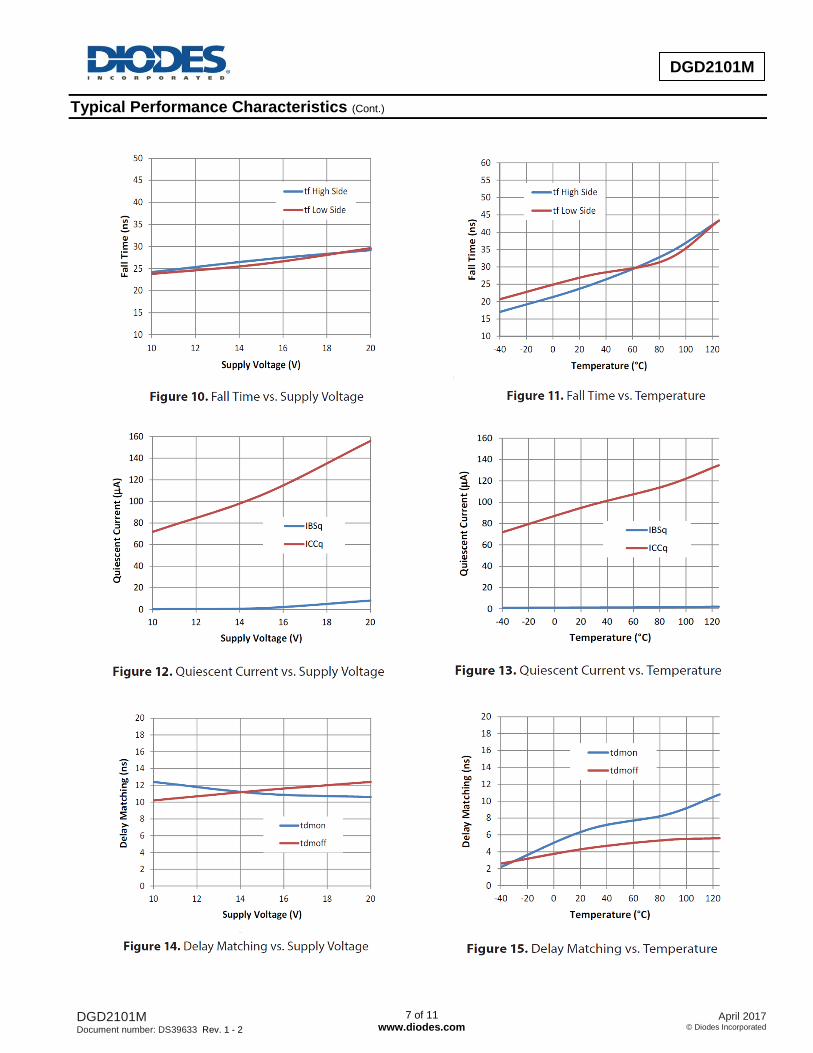
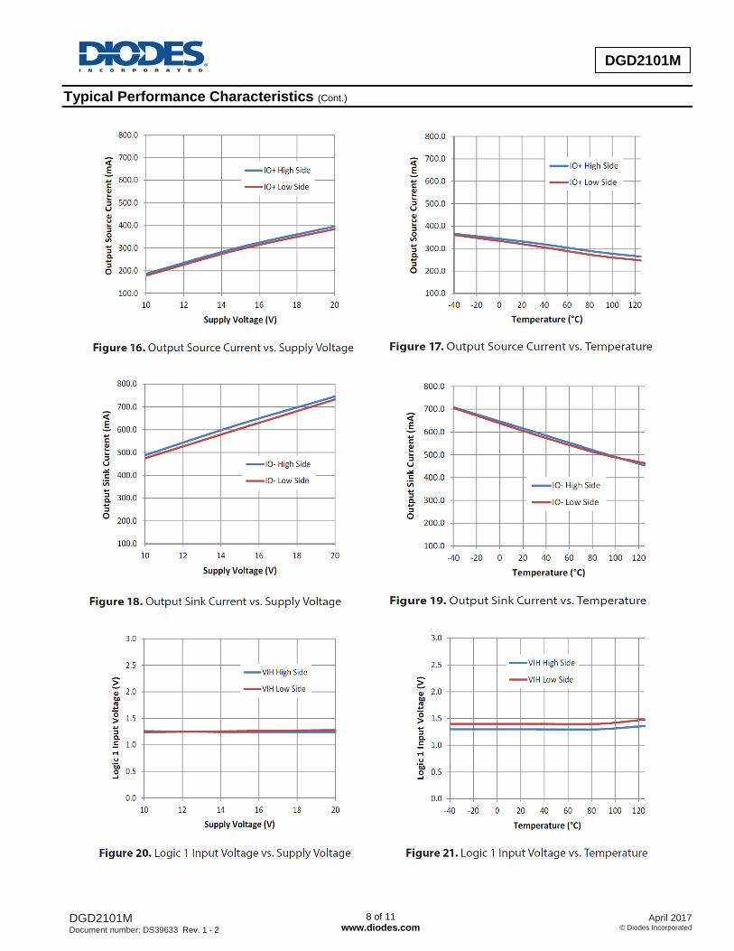
Typical Performance Characteristics (@TA = +25°C, unless otherwise specified.)
DGD2101M Document number: DS39633 Rev. 1 - 2
7 of 11 www.diodes.com
April 2017 © Diodes Incorporated
DGD2101M
Typical Performance Characteristics (Cont.)
DGD2101M Document number: DS39633 Rev. 1 - 2
8 of 11 www.diodes.com
April 2017 © Diodes Incorporated
DGD2101M
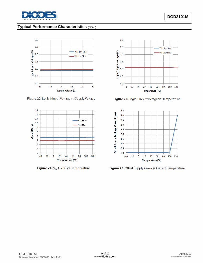
Typical Performance Characteristics (Cont.)
DGD2101M Document number: DS39633 Rev. 1 - 2
9 of 11 www.diodes.com
April 2017 © Diodes Incorporated
DGD2101M
Typical Performance Characteristics (Cont.)

DGD2101M Document number: DS39633 Rev. 1 - 2
10 of 11 www.diodes.com
April 2017 © Diodes Incorporated
DGD2101M
Package Outline Dimensions
Please see http://www.diodes.com/package-outlines.html for the latest version.
SO-8 (Type TH)
Suggested Pad Layout
Please see http://www.diodes.com/package-outlines.html for the latest version.
SO-8 (Type TH)
Note: For high voltage applications, the appropriate industry sector guidelines should be considered with regards to creepage and clearance distances between
device Terminals and PCB tracking.
SO-8 (Type TH)
Dim Min Max Typ
A 1.35 1.75 --
A1 0.10 0.25 --
A2 -- -- 1.45
b 0.35 0.51 --
c 0.190 0.248 --
D 4.80 5.00 4.90
E 5.80 6.20 6.00
E1 3.80 4.00 3.90
e -- -- 1.27
h 0.25 0.50 --
L 0.41 1.27 --
L1 -- -- 1.04
Ø 0 8 --
All Dimensions in mm
Dimensions Value (in mm)
C 1.27
C1 5.20
X 0.60
Y 2.20
b
e
E1
A2
A1
Ø
h 45°
R 0.16+/-0.02
L
Seating Plane
Gauge Plane
D
E
A
R 0.23+/-0.02
L1
0.25
c
C
C1
X
Y

DGD2101M Document number: DS39633 Rev. 1 - 2
11 of 11 www.diodes.com
April 2017 © Diodes Incorporated
DGD2101M
IMPORTANT NOTICE DIODES INCORPORATED MAKES NO WARRANTY OF ANY KIND, EXPRESS OR IMPLIED, WITH REGARDS TO THIS DOCUMENT, INCLUDING, BUT NOT LIMITED TO, THE IMPLIED WARRANTIES OF MERCHANTABILITY AND FITNESS FOR A PARTICULAR PURPOSE (AND THEIR EQUIVALENTS UNDER THE LAWS OF ANY JURISDICTION). Diodes Incorporated and its subsidiaries reserve the right to make modifications, enhancements, improvements, corrections or other changes without further notice to this document and any product described herein. Diodes Incorporated does not assume any liability arising out of the application or use of this document or any product described herein; neither does Diodes Incorporated convey any license under its patent or trademark rights, nor the rights of others. Any Customer or user of this document or products described herein in such applications shall assume all risks of such use and will agree to hold Diodes Incorporated and all the companies whose products are represented on Diodes Incorporated website, harmless against all damages. Diodes Incorporated does not warrant or accept any liability whatsoever in respect of any products purchased through unauthorized sales channel. Should Customers purchase or use Diodes Incorporated products for any unintended or unauthorized application, Customers shall indemnify and hold Diodes Incorporated and its representatives harmless against all claims, damages, expenses, and attorney fees arising out of, directly or indirectly, any claim of personal injury or death associated with such unintended or unauthorized application. Products described herein may be covered by one or more United States, international or foreign patents pending. Product names and markings noted herein may also be covered by one or more United States, international or foreign trademarks. This document is written in English but may be translated into multiple languages for reference. Only the English version of this document is the final and determinative format released by Diodes Incorporated.
LIFE SUPPORT Diodes Incorporated products are specifically not authorized for use as critical components in life support devices or systems without the express written approval of the Chief Executive Officer of Diodes Incorporated. As used herein: A. Life support devices or systems are devices or systems which: 1. are intended to implant into the body, or
2. support or sustain life and whose failure to perform when properly used in accordance with instructions for use provided in the labeling can be reasonably expected to result in significant injury to the user.
B. A critical component is any component in a life support device or system whose failure to perform can be reasonably expected to cause the failure of the life support device or to affect its safety or effectiveness. Customers represent that they have all necessary expertise in the safety and regulatory ramifications of their life support devices or systems, and acknowledge and agree that they are solely responsible for all legal, regulatory and safety-related requirements concerning their products and any use of Diodes Incorporated products in such safety-critical, life support devices or systems, notwithstanding any devices- or systems-related information or support that may be provided by Diodes Incorporated. Further, Customers must fully indemnify Diodes Incorporated and its representatives against any damages arising out of the use of Diodes Incorporated products in such safety-critical, life support devices or systems. Copyright © 2017, Diodes Incorporated www.diodes.com


![LOGIC SENSOR PROOUT Gate Driver Providing Galvanic ... · LOGIC SENSOR PROOUT Gate Driver Providing Galvanic ... ... 4]]]](https://img.pdfslide.us/doc/110x75/5f97e95f3e31877b342a40b6/logic-sensor-proout-gate-driver-providing-galvanic-logic-sensor-proout-gate.jpg)