Embed Size (px)
Citation preview

Issue 34 April 2012
Ion Implantation Part II – Process IssuesBy Christopher HendersonThis month we continue our overview of ion implantation. Thismonth we are addressing processing issues associated with ionimplantation. To access Part I in last month's newsletter, click here.In this article, we will discuss charge neutralization, energycontamination, wafer charging, wafer heating, photoresist outgassing,implant angle effects, and ultrashallow junction formation.The first process challenge we’ll discuss is charge neutralization.We know that the ions need to maintain a specific charge state duringthe implant process. However, these ions can be neutralized bycollisions with gas atoms in the chamber. This is a big problem duringboron deceleration, which is used in some implant systems to createshallow junctions. Neutral atoms are a problem because they cannotbe accelerated and steered properly with electrostatic plates. They willnot be implanted to the correct depth if the neutralization occurs earlyon; they will not be spread uniformly across the wafer if the systememploys electrostatic scanning, and they will not be counted by thedose measurement system.A different problem happens at higher energies—collisionsbetween ions and atoms can caused increased ionization. The solutionis to remove, as much as possible, the atoms from the chamber. Thismeans ultra high vacuum is required in the beamline and in thechamber. This in turn means that one must use high capacity pumpsand perform frequent regeneration of cryopumps. One should alsoavoid decelerating the beam, and one should provide neutral traps or
Page 1 Ion ImplantationPart II – ProcessIssuesPage 7 Technical TidbitPage 8 Ask the ExpertsPage 9 Spotlight on ourCourses: MEMSTechnologyPage 13 Upcoming Courses

Issue 34
2
April 2012
beam filters to remove neutral species.Charge neutralization brings up a broader issue, that of energy contamination. This situation occurswhen ions of the wrong energy are implanted. This leads to incorrect doping profiles. The main causesare charge neutralization, which we discussed, and contaminants of the same mass-to-charge ratio notbeing removed by the mass analysis magnet. An example of this would be a double-charged dualphosphorus ion in a single-charged single phosphorus ion beam. One would use the same solutions forthis problem as with charge neutralization.Another concern is contamination control. Contaminants can come from apertures, wafer holders, andmetals used in the beam line hardware. They can also come from other dopant atoms used in the systemthat have been implanted into the hardware and then resputtered. And they can come from particles ofmaterial flaked off from the beamline hardware or wafer handling system and then transported in thebeam by the electrostatic forces. This problem can be minimized by routine cleaning of the components,using materials with low sputter yield in the beamline like carbon, and dedicating implanters by speciesto prevent cross contamination.Another significant problem is wafer charging. This can result in device damage due to ESD as chargebuilds up in sensitive gates. It can also result in non-uniformity, due to the charge on the surfacedistorting the incoming beam. This is typically a problem with high current implanters. One solution is touse a system to reduce wafer charge. A common method is to use a plasma flood gun. This produces lowenergy electrons at the surface that can recombine with the charged ions. The goal here is to balance thecharge and charge flow at the surface. Another solution is to minimize the beam density by employingdual mechanical or ribbon scanning methods, moving to batch processing to increase the implant area,and increasing scan speeds to lower dwell times. This reduces the time for charge buildup.Another significant problem is heat generation. High-energy ions decelerate in the wafer, and much ofthat energy is dissipated as heat. This excess heat can damage photoresist masks, leading to criticaldimension changes, or even blistering, flaking or popping. High temperatures can also lead to dopantredistribution, as diffusion processes accelerate exponentially at higher temperatures. This can also leadto undesirable forms of crystal defects. This is mainly a problem with high power, high mass implantswhere the energy dissipation is significant. The equation below helps to illustrate the dependence onboth accelerating voltage and current. The solutions for this problem include proper wafer cooling, performing hard bake or other resiststabilization techniques, and minimizing the power density with larger beam sizes, faster scanning, andso on.Still another problem is photoresist outgassing. Energetic ions will break the resist polymer bonds,releasing hydrogen. This problem is strongly related to beam power density. The increased heat makesthe resist more susceptible to this problem. There are two main issues here. One is charge neutralization,and the other is resist mask damage. Liberated hydrogen will interfere with charge neutralization efforts.The solutions here are to optimize the resist process through hard bakes or ultraviolet photostabilization,increasing the equipment chamber size to reduce local hydrogen concentrations or use high pump speedvacuum systems, minimizing the beam power density, and conditioning the resist through a controlledramp-up of beam current for example.
Issue 34
3
April 2012
Implant angle effects also pose a challenge for process integration. There is beam shadowing thatoccurs in the channel from 7° implants, a common angle that helps minimize ion channeling. This leads tonon-symmetrical channels under the mask edge. This can be addressed through quad implants or throughzero degree implants. Some newer implanters can also achieve these effects through beam steering.Another implant angle effect is variation in implant angle in a batch processor. Wafers at the outsidereceive a different angle implant than those at the center. The solution here is to go to a single waferimplanter with parallel scan to minimize the effect.Figure 1 groups most common implant applications together so that we can visualize the differences.The chart shows the applications as a function of energy and dose. We start with the highest dose, lowestenergy implants, moving toward the lower dose, high energy implants. High current implants are typicallydone close to the surface, and are done later in the process, so one requires heavier doping to overcomethe doping from previous implants. Medium current implants are performed to create the transistor wellsand isolation regions, and to determine the transistor channel properties. High energy implants are doneto create isolation regions, wells, and deep wells for some types of bipolar or BiCMOS transistors. They canalso be used for charge-coupled device structures.
Figure 1: Chart showing applications as a function of energy and dose.Medium current implants are used for both well and channel engineering. Channel engineering is usedto control the drive characteristics of the transistor, and well engineering is used to control the isolation
Issue 34
4
April 2012
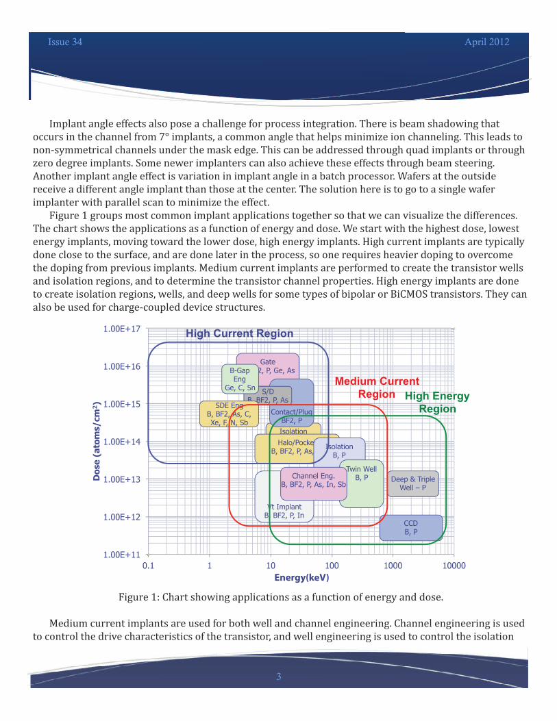
between transistors. The three common channel engineering implants are the halo implant, the thresholdadjustment implant, and the super steep retrograde or SSR implants. The three well engineering implantsare for shallow wells, deep wells, and channel stops.Some medium current implants, their dose ranges, energy ranges, and tilts are given in this table.Medium current implants can include layers done close to the surface, like halo implants or thresholdadjust implants, or layers put in further below the silicon surface, like deep well structures.
Figure 2: Applications for medium current implants.Mid Current ImplantsImplant Dose Range (cm-2) Energy Range (keV) TiltChannel EngineeringHalo 1e13 – 6e13 2 – 40 YesVt 5e11 – 5e12 5 – 40 NoSSR 5e11 – 8e12 100 – 200 NoWell EngineeringShallow well 8e12 – 3e13 100 – 600 NoDeep well 6e12 – 1e13 800 – 1200 NoChannel stop 5e12 – 1e13 80 – 200 NoFigure 3: Table showing typical energies and doses for medium current implants.
Issue 34
5
April 2012
High dose applications are used for heavily doped regions. These include source-drain regions as wellas their extensions, polysilicon gate doping, and pre-amorphization implantation.High Dose ImplantsImplant Dose Range (cm-2) Energy Range (keV) TiltSource/Drain 8e14 – 5e15 1 – 5 NoSDE 5e14 – 5e15 0.2 – 5 LowGate Doping 5e15 – 5e16 2 – 5 NoPAI 5e14 – 1e15 10 – 30 NoFigure 4: Table showing typical energies and doses for high dose implants.A final remaining challenge is ultra-shallow junction or USJ formation. Ultra-shallow junctions arecritical for today’s nanometer-scale ICs. The big challenge with ultra-shallow junctions is the boronimplant. Boron is a small atom and is therefore easily accelerated in the beam that leads to a highprojected range and straggle. To reduce this variability, low energies are required, so beam deceleration isused. Another challenge is low beam current. The need for beam deceleration leads to beam blow up thatrequires a lower beam current. Lower energies also cause increased sputtering of the silicon surface.Lower energies also lead to increase backscattering of boron atoms. At 500 volts, there is a 10% boronloss, and it increases to a 20% loss at 200 volts. Furthermore, these effects increase with accumulateddose. Finally, transient-enhanced diffusion creates problems, where the silicon damage leads to increasedmovement of boron atoms.The goal with ultra-shallow source drain regions is to create 50 to 100 nm deep junctions and 30 to 60nm junctions for the extensions with minimal dopant redistribution and residual damage. One method todo this is to implant boron difluoride (BF2) instead of pure boron. This was a common technique in olderprocesses and overcomes the deceleration problem, since the heavier molecule is not accelerated as muchto begin with. However, the fluorine atoms contribute to boron sputtering.
Issue 34
6
April 2012
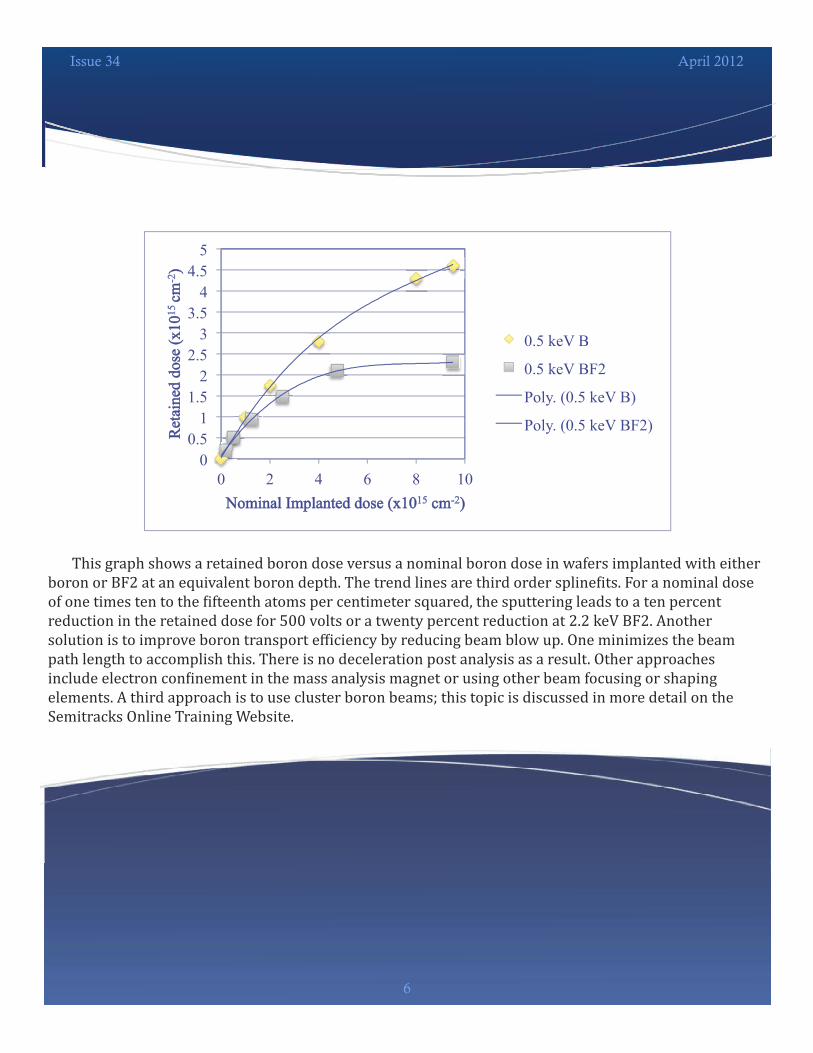
This graph shows a retained boron dose versus a nominal boron dose in wafers implanted with eitherboron or BF2 at an equivalent boron depth. The trend lines are third order splinefits. For a nominal doseof one times ten to the fifteenth atoms per centimeter squared, the sputtering leads to a ten percentreduction in the retained dose for 500 volts or a twenty percent reduction at 2.2 keV BF2. Anothersolution is to improve boron transport efficiency by reducing beam blow up. One minimizes the beampath length to accomplish this. There is no deceleration post analysis as a result. Other approachesinclude electron confinement in the mass analysis magnet or using other beam focusing or shapingelements. A third approach is to use cluster boron beams; this topic is discussed in more detail on theSemitracks Online Training Website.

Issue 34
7
April 2012
Technical TidbitApplications of the Coffin-Manson ModelMost of us are familiar with the basic Coffin-Manson model, but there are actually several variations tothis model that can be quite useful. Read on for more details.The basic Coffin-Manson model is shown here:where Nf is the number of cycles to fatigue, C0 is a constant, ΔT is the temperature cycling ranging, and
c is the Coffin Manson exponent. There are several other forms of the equation that are used to modelfailures in semiconductor components and electronic systems. We’ll discuss these below.Another version of the formula takes into account that there may be elastic as well as plasticdeformation that occurs. Elastic deformation will not cause cracking; only plastic deformation does.Therefore, one should subtract the temperature range associated with elastic deformation out of theformula. One can modify the Coffin Manson model like this to take this into account:where ΔT0 is the temperature range where elastic deformation occurs. The reason that one sees themain effect being low temperature is that ΔT – ΔT0 is greater in this scenario. For example, let’s assumethat the elastic deformation region (ΔT0) extends 50°C below neutral stress at 150°C, or to 100°C. If wetemperature cycle from -55°C to +125°C, then ΔT – ΔT0 is 155°. If we temperature cycle from 0°C to+125°C, then ΔT – ΔT0 is only 100°. Therefore the minimum temperature has the most impact. Absolutetemperature swings will also factor in as well.Another form of the Coffin-Manson model is the Norris-Landzberg Model. It is used for modelingcracking on solder materials. It is written like this:The acceleration factor for the Norris-Landzberg model is given by:The parameters for lead-tin solder are typically n = 1.9, m = 0.33, and Ea = 0.122eV. For lead-freesolders, engineers typically use n = 2.65, m = 0.136, and Ea = 0.189eV.
Issue 34
8
April 2012
Ask the Experts
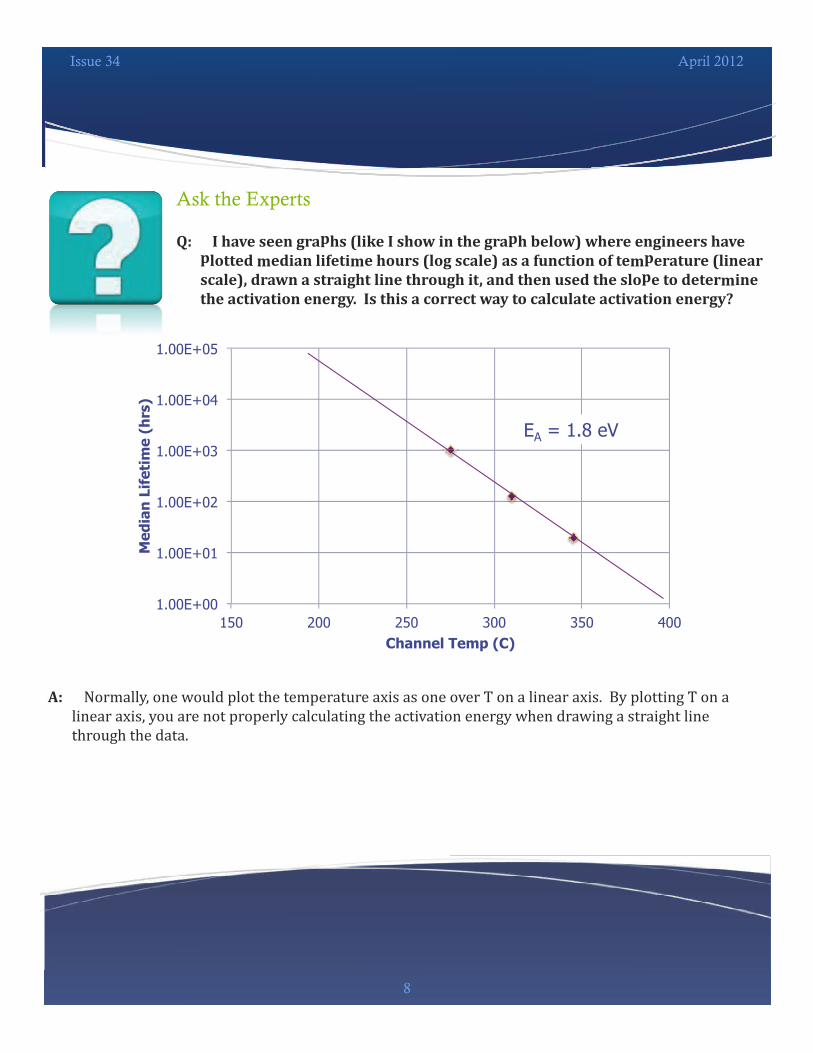
Q: I have seen graphs (like I show in the graph below) where engineers haveplotted median lifetime hours (log scale) as a function of temperature (linearscale), drawn a straight line through it, and then used the slope to determinethe activation energy. Is this a correct way to calculate activation energy?
A: Normally, one would plot the temperature axis as one over T on a linear axis. By plotting T on alinear axis, you are not properly calculating the activation energy when drawing a straight linethrough the data.
Issue 34
9
April 2012
Spotlight on our Courses: MEMS TechnologyOur MEMS Technology Course will be offered in Enschade, Netherlands, June 12 – 13 this year. Here ismore information about the course. If there is sufficient demand, we'll also offer it in the US later this year.If you're interested in having this course as an in-house course for your staff, please feel free to contact usat (505) 858-9813, or at [email protected] Systems (MEMS) have captured the interest of the public with their promiseto miniaturize existing systems. Although much of the excitement surrounding MEMS has died down, realapplications are beginning to emerge. MEMS accelerometers for games, automotive, and wirelessapplications have emerged. MEMS inkjet chips are now ubiquitous, and new applications for RF andsensors are in development. One of the most challenging aspects of MEMS is packaging. Forces thatnormally do not affect meso-scale objects must be understood and controlled at the micro-scale. This hascreated a number of challenges related to the packaging of these components. MEMS Technology is a 2-day course that offers detailed instruction on the design, processing, packaging, and reliability of MEMSdevices. We place special emphasis on DRIE, surface-to-volume ratio issues, electrostatics, liquid wetting,inertia, and other parameters. The course also contains a number of models and simulations used inconjunction with MEMS devices. This course is a must for every manager, engineer, and techniciandesigning MEMS devices, using MEMS components in high performance applications or new packagingconfigurations, or supplying packaging tools to the industry.By focusing on the fundamentals of MEMS devices and packaging, participants will learn whyadvances in the industry are occurring along certain lines and not others. Our instructors work hard toexplain MEMS Technologies without delving heavily into the complex physics and materials science thatnormally accompany this discipline.Participants learn basic but powerful aspects about these unique devices. This skill-building series isdivided into three segments:1. Device Design and Processing. Participants review the basic wafer processing steps for MEMSdevices, including deep reactive ion etching, wet etching, patterning, CMP, and more.2. MEMS Packaging. Participants learn the fundamentals of packaging concepts for MEMS devices.They learn about structural release, cleaning, encapsulation, and basic testing. They also discussthe challenges associated with packaging.3. MEMS Reliability. Participants learn MEMS reliability issues and associated analysis andsimulation techniques. They also learn about the physics and mechanics issues involved inreliability degradation of MEMS devices.COURSE OBJECTIVES1. The seminar will provide participants with an in-depth understanding of MEMS and its technicalissues.2. Participants will learn the unique processing steps related to MEMS technology, including deepreactive ion etching, non-standard silicon orientation wafers, and special thin-films and coatingsfor moving components.

Issue 34
10
April 2012
3. Participants will understand the basic concepts behind thermal and mechanical simulations ofMEMS packages.4. The seminar will identify the key issues related to the success of MEMS packaging. This includesthe need for understanding charge, release, and package environments.5. The seminar offers a wide variety of sample modeling problems that participants work in class tohelp them gain knowledge of the fundamentals of MEMS packaging.6. Participants will be able to identify basic and advanced principles for mechanical stress, charge,and thermal diffusion.7. Participants will understand how process, release techniques, and packaging are interrelated.8. Participants will be able to make decisions about how to construct and evaluate new MEMSpackaging designs and technologies.9. Participants will also be introduced to wafer-level simulations, which are important to MEMSpackages.INSTRUCTIONAL STRATEGYBy using a combination of instruction by lecture, classroom exercises, and question/answer sessions,participants will learn practical information on semiconductor packaging and the operation of thisindustry. From the very first moments of the seminar until the last sentence of the training, the drivinginstructional factor is application. We use instructors who are internationally recognized experts in theirfields that have years of experience (both current and relevant) in this field.COURSE OUTLINE1. Introduction to MEMS Technologies1.1. Basic Concepts1.2. MEMS-related Definitions1.2.1. MEMS Mechanics1.2.1.1. Mechanical/Thermal1.2.1.2. Microfluidics1.2.2. MEMS Physics1.2.2.1. Electrical/Optical1.2.2.2. Joule Heating1.3. From MEMS to NEMS2. MEMS Device Design & Function2.1. Piezoelectric Inkjet Heads2.2. Accelerometers & Gyroscopes2.3. Flow & Pressure Sensors2.4. Micromachines & Micromotors2.5. Optical Display & Switching Devices2.5.1. RF-MEMS & MOEMS2.6. Designing & Simulating Operation2.7. Linear Actuation, Comb-Drive Actuation, & Resonators

Issue 34
11
April 2012
3. MEMS Device Processing3.1. Lithography, Patterning, & Lift-off3.2. Etching3.3. Deposition3.4. Sacrificial & Structural Layers4. MEMS Assembly, Packaging, & Testing4.1. Packaging Types & Options4.2. Structural Release4.3. Die Attach Process4.4. Interconnects4.5. Gettering4.6. Encapsulation & Capping4.7. When and How Should We Test?5. MEMS Reliability5.1. Device-Level Failure Mechanisms5.1.1. Stiction (Release- or Shock-related) and Wear5.1.2. Particle Contamination5.1.3. Electrostatic discharge (ESD) & Electrical Overstress (EOS)5.2. Package-Level Failure Mechanisms5.2.1. Thermomechanical Stress & Fatigue5.2.2. Shock & Vibration5.2.3. Moisture/Corrosion5.3. Use Condition Failure Mechanisms6. MEMS Device Trends6.1. Increased Functionality6.2. Spin-off Opportunities6.3. New MEMS Products7. Conclusions

Issue 34
12
April 2012
Semitracks will appear at the
International Reliability Physics SymposiumApril 15 – 19
Anaheim, California
Stop by and see us!
http://www.irps.org
Issue 34
13
April 2012
Upcoming Courses(Click on each item for details)Copper Wire BondingMay 7 – 8, 2012 (Mon. – Tues.)Munich, Germany
Failure and Yield AnalysisMay 7 – 10, 2012 (Mon. – Thurs.)Munich, GermanySemiconductor ReliabilityMay 14 – 16, 2012 (Mon. – Wed.)Munich, Germany
Polymers and FTIRMay 21 – 22, 2012 (Mon – Tues)Penang, MalaysiaPolymers and FTIRMay 24 – 25, 2012 (Thurs – Fri)Melaka, Malaysia
Wafer Fab ProcessingJune 5, 2012 (Tues)San Jose, CA, USAMEMS TechnologyJune 12 – 13, 2012 (Tues – Wed)Enschede, Netherlands
Reliability ChallengesJune 11, 2012 (Wed)San Francisco, CA, USACopper Wire BondingJuly 11 – 12, 2012 (Mon. – Tues.)San Francisco, CA USA
FeedbackIf you have a suggestion or a comment regarding our courses, onlinetraining, discussion forums, or reference materials, or if you wish tosuggest a new course or location, please call us at 1-505-858-0454 orEmail us ([email protected]).To submit questions to the Q&A section, inquire about an article, orsuggest a topic you would like to see covered in the next newsletter,please contact Jeremy Henderson by Email([email protected]).We are always looking for ways to enhance our courses and educationalmaterials.~For more information on Semitracks online training or public courses,visit our web site!http://www.semitracks.comTo post, read, or answer a question, visit our forums.
We look forward to hearing from you!