Embed Size (px)
Citation preview

ion Implantation of boron in germanium Kevin S. Jones2 ) and E. E. Haller Lawrence Berkeley Laboratory and University of California, Berkeley, California 94720
(Received 22 September 1986; accepted for pUblication 7 November 1986)
The activation of boron implanted at room temperature into germanium has been studied. In contrast to other group III elements boron forms a p-type layer before any
postl.1nplant annealIng steps. Variable temperature Hall effect measurements and deep level trans{ent spectroscopy experiments indicate that all of the boron ions are electricaHy active as shallow acceptor the en.tire dose range (5 X 101l/cm2 to 1 X 10¹⁴/cm2 ) and energy range (25-100 keY) mvestlgated, WIthout any postimplant annealing. The concentration of damage rel.ated acceptor is only 10% of the boron related, shaUow accepted centers concentrailon for low-energy implants (25 keY), but becomes dominant at high energies (100 keY) and low doses ( < 1 X 10¹²/cm2 )0 Three damage related hole traps are produced by . 1 . f11B+ Imp antatlOn 0 . Two of these hole traps have also been observed in y-irradiated Ge and may be oxygen-vacancy related defects, while the third trap may be divacancy related. All three :raps anneal out at low temperatures ( < 300 ·C). Room-temperature implantation of BFt mto Ge, does not lead to substitutionally active boron without annealing. A thermal cycle of 350 ·C for 30 min activates 100% of the boron.
t INTRODUCTION Ion implantation of boron has proven to be invaluable in
the fabrication of p 4- contacts on ultrapure germanium. The problem with diffused contacts is one of contamination. Copper diffuses interstitially and forms a deep triple accep-tor as well as complexing with hydrogen to form additional deep acceptors. At typical diffusion temperatures for germa-nium (600 ·C) the solid solubility ofCu is 1014/cm3 or -4 orders of magnitude above the background concentra-tion. As no adequate p + diffused contacts can be produced at low temperatures ( < 500 ·C) in Ge the need for ion implant-ed contacts is apparent.
As summarized by Ponpon et al. 1 boron appears to be the best group nIA ion for the fabrication ofp"" contacts in germanium due to its relatively small amount of damage production and the results of Alton and Love2 which have shown the resistivity of aluminum implants in Ge to be twice that of baron implants for anneal cycles below 450 ·C and at a dose of 5X 10¹⁴/cm2 (a typical dose for a heavily doped contact).
Implantation of boron ions into germanium exhibits some unique phenomena. For every other ion implanted into silicon or germanium, some form of postimplant annealing step is necessary to achieve a significant electrical activation of the doping species. However, implantation of boron at a typical dose of 1 X 10¹⁴/cm2 into germanium produces a peak acceptor center concentration of at least 1 X 101I1
/ em3
prior to annealing. This concentration is sufficient to achieve a p-type contact without a postimplant annealing step. In fact, upon annealing the value of the sheet resistivity of a boron implanted layer shows no step decrease, characteristic of an implanted ion being activated. 1,3 Others have reported different results of a small resistivity step2 and even a type
"Current address: Department of Materials Science and Mineral Engineer-ing, Hearst Milling Building. University of California, Berkeley, CA 94720,
change from n type to p type upon annealing.4 One of the questions that arises is, what is the source of the electrical activity associated with ion implantation of boron into ger-manium? Is the boron substitutional upon implantation and thus the source of the free holes or is the p-type conductivity due to lattice damage including possibly 11 variety ofooron-defect complexes?
One reason for questioning the source of the conductiv-ity, aside from its unusual annealing nature, is the published Rutherford backscattering (RBS) resule which shows a damage peak for 30-ke V boron ions implanted into germani-um. This damage peak is shown to anneal away by 170°C, Other observations include the effect of the temperature of the germanium during the implantation. As the substrate temperature drops from 130·C to - 90 'C the normalized disorder increases from 3 to 100% for a 56 keY, 6X 10141 cm2 implant. 5 This result implies that a significant amount of annealing occurs around room temperature. Additional RES results indicate that implantation of boron into germa-nium produces 10 times as much damage as room tempera-tune.5 It is known that a post implant annealing step is re-quired to electrically activate boron implanted into silicon. These two results might imply that the as implanted electri-cal activity of boron in germanium may be due to damage related acceptor centers.
From these results, it appears the nature of the electrical activity of implanted boron contacts on germanium is an issue worthy of further investigation.
II. EXPERIMENT: HALL EFFECT Hall measurements are most commonly used to deter-
mine the free-carrier concentration. The Van der Pauw6 con-figuration, shown in Fig. 1, was chosen for our experiments. As the implanted layer is p type from either damage related acceptor centers or substitutional implanted boron, an n type (1 X lO B /em3 ) substrate was used in order to isolate the implanted layer upon cooling of the sample. The
2469 Jo Appl. Phys, 61 (7), 1 April 1987 0021-8979/87/Q72469-09$02.40 © 1987 American Institute of Physics 2469
Downloaded 04 Apr 2011 to 128.227.135.101. Redistribution subject to AIP license or copyright; see http://jap.aip.org/about/rights_and_permissions
FIG, L Van de!:' Pauw Hall effect sample geometry for studying implanted layers, Region A: Ion implanted contacts on all four top surface comers (roo-keV B, 5X lO!4/cm', annealed). Region 13: Ion implant entire top sur-face with species to be studied.
nium used was grown from a silica crucible under a hydro-gen ambiant and was doped with phosphorus. The isolation process involves the formation of a p-n junction at the depth where the implant p-type concentration equals the sub-strates' n-type doping. The electrical measurements are made via p-type (II B) contacts which were implanted on the top surface corners and annealed prior to implanting the species to be studied. The wafer orientation was (113) and the sample was tilted 7° oft' axis during implantation. The germanium used is intrinsic at room temperature, therefore Hall effect measurements made at this temperature corre-spond to measuring the hole concentration in the implanted layer and the electron and hole concentrations in the intrin· sic substrate. Upon cooling, the intrinsic carrier concentra-tion decreases rapidly. Once the intrinsic carrier concentra-tion is less than the n-type doping concentration of the substrate, electrons from the donor centers dominate the free-carrier concentration of the substrate. At this tempera-ture, a p-n junction forms in the tail region of the implanted layer and at subsequently lower temperatures, only the im-planted layer is measured via the p-type contacts.
m. RESULTS AND DISCUSSION
A. implantation dose effects
In studying the effect of dose in these implantation ex-periments the energy of the implant was kept constant at 100 keY. The dose range investigated ranged from 5 X 101l/cm2 to 1 X 10¹⁴/cm2. The projected range for a lOO-keV boron implant in Ge is around 2550 A with a standard deviation of 1150 A,3 For a 1 X 10¹⁴/cm2 implant dose the peak concen-tration is about 3,5 X lOlS/em3 which is well above the Mott transition concentration. Thus, at this dose, conduction in the region whose concentration is above the Matt transition occurs via impurity banding due to the overlap of the elec-tronic wave functions. The region of the implanted profile where the concentration is below the Mott transition affects the Hall coefficient and is responsible for the "dip" in con-centration observed with VTHE of high dose
2470 J. Appl. Phys., Vol. 61, No. 7,1 April 19S7
(> IX 1013/cm2for lOOkeV) implants. This wi11 be expand-ed upon later.
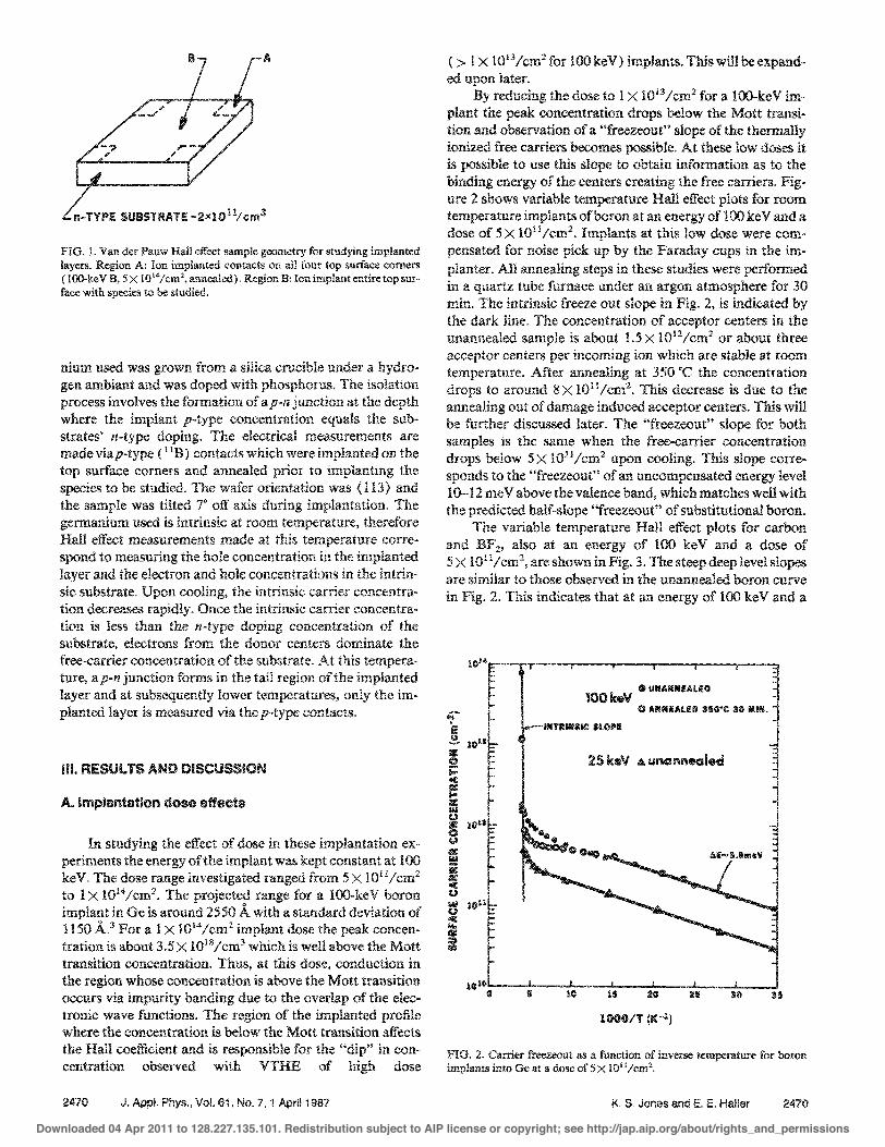
By reducing the dose to 1 X 10¹³ /cm2 for a lOO-keV im-plant the peak concentration drops below the Mott transi-tion and observation of a "freezeout" slope of the thermally ionized free carriers becomes possible. At these low doses it is possible to use this slope to obtain information as to the binding energy of the centers creating the free carriers. Fig-ure 2 shows variable temperature Hall effect plots for room temperature implants of boron at an energy of 100 ke V and a dose of 5X 101l/cm2 • Implants at this low dose were com-pensated for noise pick up by the Faraday cups in the im-planter. All annealing steps in these studies were performed in a quartz tube furnace under an argon atmosphere for 30 min. The intrinsic freeze out slope in Fig. 2, is indicated by the dark line. The concentration of acceptor centers in the unannealed sample is about 1.5 X 1Ol2/cm2 or about three acceptor centers per incoming ion which are stable at room temperature. After annealing at 350·C the concentration drops to around 8 X IOll/cm2 . This decrease is due to the annealing out of damage induced acceptor centers. This will be further discussed later. The "freezeout" slope for both samples is the same when the free-carrier concentration drops below 5X 10¹¹/cm2 upon cooling. This slope corre-sponds to the "freezeout" of an uncompensated energy level 1 0---12 me V above the valence band, which matches well with the predicted half-slope "freezeout" of substitutional boron.
The variable temperature Hall effect plots for carbon and BFz, also at an energy of 100 keY and a dose of 5 X 101l/cm2, are shown in Fig. 3. The steep deep level slopes are similar to those observed in the unanneaIed boron curve in Fig. 2. This indicates that at an energy of 100 keY and a
• U"AKNfAlIED 100k.V o ANNUllED 350'C 30 IIl!N.
25 k.V A unannealed
FIG. 2. Carrier freezeout as a function of inverse temperature for boron implants into Ge at a dose of 5 X lO" /cm2•
K. S. Jones and E. E. Hailer 2470
Downloaded 04 Apr 2011 to 128.227.135.101. Redistribution subject to AIP license or copyright; see http://jap.aip.org/about/rights_and_permissions
III 14
if" !
"l z Q i= c II: l-X W U z 8 = w Ii 0: C U w t:I C 100 II: :::,) II)
10101 c
III III "
• I(
III " ill. "
ill
J f
\I 10 15
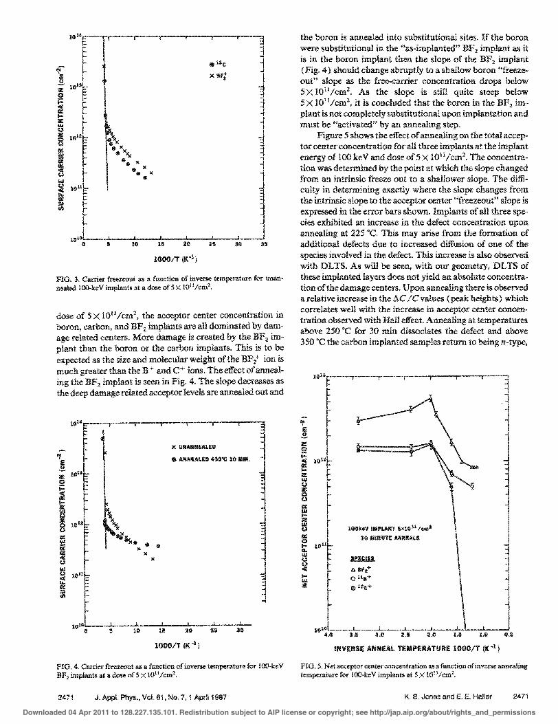
FIG. 3. Carrier freezoout as II function of inverse temperature for unan-nealed lOO-keVimplants at a dose of5X 101I/cm2
•
dose of 5X lOll/cm2, the acceptor center concentration in boron, carbon, and BFz implants are all dominated by dam-age related centers. More damage is created by the BF2 plant than the boron or the carbon implants. This is to be expected as the size and molecular weight of the BFt ion is much greater than the B+ and C+ ions. The effect of anneal-ing the BF2 implant is seen in Fig. 4. The slope decreases as the deep damage related acceptor levels are annealed out and
X IINAIiiNULED
• ANNEALED 450"C 30 MIft.
100011' (I( -1)
FIG. 4. Carrier freezeout as II function ofinverse temperature for tOO-keV BFz implants at a dose ofS X 1011/cm2•
2411 J. AppL Phys., Vol. 61. No.7. 1 April 1987
the boron is annealed into substitutional sites. If the boron were substitutional in the "as-implanted" BF2 implant as it is in the boron implant then the slope of the BFz implant (Fig. 4) should change abruptly to a shallow boron "freeze-out" slope as the free-carrier concentration drops below 5X lOiI/cruz. As the slope is still quit.e steep below 5X lOll/cmz, it is concluded that the boron in the BF2 im-plant is not completely substitutional upon implantation and must be "activated" by an annealing step.
Figure 5 shows the effect of annealing on the total accep-tor center concentration for all three i.mplants at the implant energy of 100 keY and dose ofS X lOll/om:!, The concentra-tion was determined by the point at which the slope changed from an intrinsic freeze out to a shallower slope. The diffi-culty in determining exactly where the slope changes from the intrinsic slope to the acceptor center "freezeol.lt" slope is expressed in the error bars shown. Implants of all three spe-cies exhibited an increase in the defect concentration upon annealing at 225°C. This may arise from the formation of additional defects due to increased diffusion of one of the species involved in the defect. This increase is also observed with DLTS. As will be seen, with our geometry, DLTS of these implanted layers does not yield an absolute concentra-tion of the damage centers, Upon annealing there is observed a relative increase in the IJ.C / C values (peak heights) which correlates well with the increase in acceptor center concen-tration observed with Hall effect. Annealing at temperatures above 250·C for 30 min dissociates the defect and above 350 ·C the carbon implanted samples return to being !Hype,
'1 E ..2. z I:)
1012 < fIl: I-Z &II U Z 0
1 t:I iii: iii I-Z W lOOI<4IV IMPLANT 5><10 II Ie",! t:I III: 30 MIPlUT!!: ANftEA!..S 0 lOll I-A. I.!.! J£WU. u (,)
I:> 1If',+ <if: I- oUa+ w Z @UC'"
INVERSE ANNEAL TEMPERATURE 1000/1 (K -1)
FIG. 5. Net acceptor center concentration as a function of inverse annealing temperature for lOO-keV implants at S X 1O!l/cm2•
K. S. Jonas and E. E. Haliar 2471
Downloaded 04 Apr 2011 to 128.227.135.101. Redistribution subject to AIP license or copyright; see http://jap.aip.org/about/rights_and_permissions

i.e., the p-type damage is annealed such that the background n-type doping is dominant. Subtraction of the carbon dam-age related acceptor center concentration from the boron related acceptor center concentration does not yield accu-rate quantitative information on the boron concentration as observed by the slope change in Fig. 5, noted previously. One explanation for this may be that carbon implants produce a slightly greater concentration of damage related acceptor centers, which are stable at room temperature, than the bo-ron implants. Thus, at this low dose, the carbon implants may have limited quantitative application to boron im-plants, but the qualitative annealing behavior for boron and BFz implants is sufficiently similar to the carbon implants behavior to conclude that damage related acceptor centers do indeed dominate this low dose, high implant energy ex-treme> The concentration of acceptor centers in the boron implanted samples drops to about 5 X lOll /cm2 by 550°C while the concentration of acceptor centers in the BF2 im-planted samples drops only to 8X 10¹¹/cm2
• The difference in concentration may arise from some electrically active de-fect associated with fluorine.
Contamination problems occurred for anneal tempera-tures above 600 "C. Additional investigations indicate that the n-type substrate changes to p-type at about 600°C due to Cu contamination. Precautions were taken to avoid conta-mination including a slow postannealing cooling step to avoid "quenching in" large Cu concentrations by promoting eu precipitation.
The effect of increasing the dose on the acceptor center concentration in boron and carbon implanted samples is shown in Fig. 6. All samples were implanted at room tem-perature and were measured in the "as implanted" state. As the dose increases the number of defect-related, acceptor centers, stable at room temperature, per incoming ion de-creases. However, the concentration of acceptor centers aris-ing from shallow acceptor levels becomes constant at one per
o He !MPLANTS L:. .. c iMPlANTS
IMPLANT DOSE (em-2 )
10"
FIG. 6. Net acceptor concentration as a function of implant dose for 100-keY implants into Ge prior to annealing.
2472 J. Appl. Phys., Vol. 61, No.7,; April 1987
incoming boron ion at doses above 1 X 10¹³ /cm2• As we have just concluded that the boron is substitutional "as implant-ed" at the low dose extreme, Fig. 6 indicates that for a room temperature lOO-keV implant the boron is active upon im-plantation over the entire range of doses studied. Any in-crease in free carriers at low doses must arise from damage related acceptor levels and the concentration of these levels is greater than the concentration of shallow boron related acceptor levels at doses below 1 X 10¹²/cm2,
The variable temperature Hall effect results for a 100-keY boron implant at a dose of 1 X 10¹⁴jcm2 are shown in Fig. 7. Implants of lOO-keV boron into Ge at doses greater than 1.5 X 10¹³/cm2 yield peak concentrations above the Mott transition and banding conduction occurs. For bulk Ge doped above 5X 10¹⁷/cm3, the Hall coefficient, R H , is independent of temperature> 8 However, as seen in Fig. 7, for implanted layers the Hall coefficient is not independent of temperature between 200 and 10 K. This deviation can be explained theoretically by the following equation. Assuming there are no circulating currents and f-l H = f.l the surface Hall coefficient, R s , can be expressed as9
Rs = , n (x)f.l (x )dX)2
where n(x), p,(x) are the concentration and the mobility as a function of depth, respectively. The junction depth is t and e is the change of an electron.
Upon cooling through the upper temperature region (200 K> T> 30 K) the rapidly increasing mobility of the lower doped regions (those around the peak with concentra-tions less than 1 X 10¹⁶/cm3 ) contribute significantly to in-creasing the value of R, ' Upon further cooling the carriers in these lower doped regions (those not above the Mott transi-tion) "freezeout" and these high mobility regions become
• UNANNEAI.ED 'l' X ANNULED 350'C 30 11111'1. E
z 0 i= < !II: P. " Z IloI (.) • z 0 (.) " " ..
1 w " ,. • • iii: " .. " • .x GO It •
.:( t.) w t.) C I.L. J " ;:) III
I) 10 20 3& 40 50 60 70
lOGOn (I( -1)
FIG. 7. Carrier freezeout as a function of in verse temperature for a lOO-ke V boron implant of dose of 1 X 1O'4/cm2.
K. S. Jones and E. E. Hailer 2472
Downloaded 04 Apr 2011 to 128.227.135.101. Redistribution subject to AIP license or copyright; see http://jap.aip.org/about/rights_and_permissions
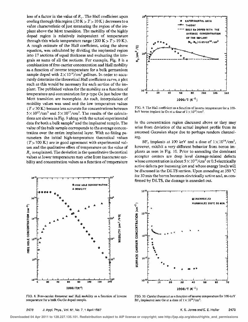
less of a factor in the value of Rs. The Hall coefficient upon cooling through this region (30 K > T> 10K) decreases to a value characteristic of just measuring the region of the im-plant above the Mott transition. The mobility of the highly doped region is relatively independent of temperature through this whole temperature range (200 K> T> 10 K). A rough estimate of the Hall coefficient, using the above equation, was calculated by dividing the implanted region into 11 sections of equal thickness and evaluating the inte-grals as sums of all the sections. For example, Fig. 8 is a combination of free-carrier concentration and Hall mobility as a function of inverse temperature for a bulk germanium sample doped with 2x lOj4/cm3 gallium. In order to accu-rately determine the theoretical Hall coefficient curve, a plot such as this would be necessary for each section of the im-plant. The published values for the mobility as a function of temperature and concentration for p-type Ge just below the Mott transition are incomplete. As such, interpolation of mobility values was used and the low temperature values ( T < 30 K) became less accurate for concentrations between 5 X 101.'i /em3 and 5 X lOn/em3. The results of the calcula-tions are shown in Fig. 9 along with the actual experimental data for both a bulk sampleS and the implanted sample. The value of the bulk sample corresponds to the average concen-tration over the entire implanted layer. With no fitting pa-rameters the initial high-temperature theoretical values (T> 100 K) are in good agreement with experimental val-ues and the qualitative effect of temperature on the value of Rs is explained. The deviation in the quantitative theoretical values at lower temperatures may arise from inaccurate mo-bility and concentration values as a function of temperature
• fl!U 1I0LE CCNCElfl'RATIOIl .to MOIIIU'fY •••• e • • • • A A
':' • AA E • A IIfJ Iii" .& • A I- A" • 011:
II:: A '" l- e Ii 4. E • ..:!. w A (,) >-Z &. • I-0 • ::i (,) iii "" • 0 ..I it Z 0 :II: 101 it ! • •
1010 lOa 0 20 40 to 10 100 120 140
lOGOff!!!:-!)
FIG. 8. Free-carrier freezeout and Hall mobility as it function of inverse tempe1'lltJ.1re for it bulk Ga:Ge doped sample.
2413 J. Appl. Phys., Vol. 61, No.7, 1 April/Sa?
• EXf'!lUMfIllTIII. ElATA -W- THEORY --- BULK Go DCI'IlD WiTH THE
&. 19
AVEliAliE COIICI!!PlTI'IATiOPI Of Till! HiI!'!,ANT
(rip. _No )=1.0!5XIOll l e .... 3
lOGO/T (I< -1 )
FIG. 9. The Hal! coefficient as a function of inverse temperature for it 100-keY boron implant in Ge at It dose of 1 X 10¹⁴/cm2,
in the concentration region discussed above or they may arise from deviation of the actual implant profile from its assumed Gaussian shape due to perhaps random channel-ing.
BF2 implants at 100 keY and a dose of 1 X lO,4/cm2,
however, exhibit a very different behavior from boron im-plants as seen in Fig. 10. Prior to annealing the dominant acceptor centers are deep level damage-related defects whose concentration is about 5 X 10¹³/cm2 or O. 5 electrically active defects per incoming ion and whose energy levels will be discussed in the DLTS section. Upon annealing at 350 QC for 30 min the boron becomes electrically active and, as con-firmed by DL TS, the damage is annealed out .
G
:IE 0 ;:: 011: 0:: l-:IE w CJ E 0 (,)
0:: to! ;: §I: c U !AI
u. II: :;, m
"
"
"
J\
• UNAHNEIII.ED XANNEALEO 3!50'C 30 MIN.
FIG. 10. Carrier freezeout as II function of inverse temperature for lOO-keV BF. implanted into Ge at II dose of 1 X 1O!4/cm2,
K. S. Jones and E. E. Haller 2473
Downloaded 04 Apr 2011 to 128.227.135.101. Redistribution subject to AIP license or copyright; see http://jap.aip.org/about/rights_and_permissions
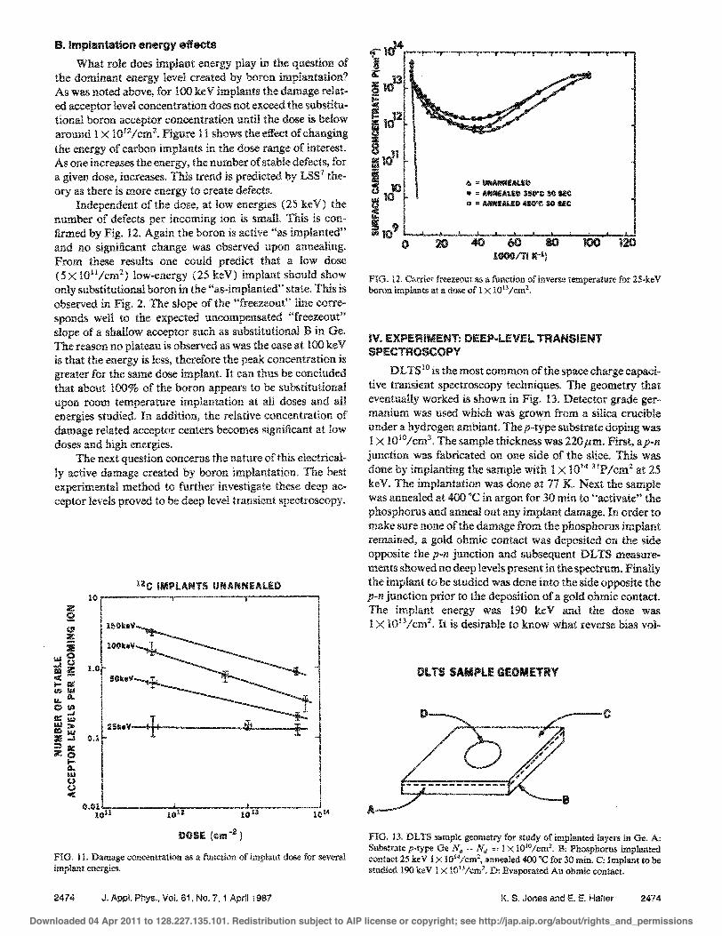
B. Implantation energy effects What role does implant energy play in the question of
the dominant energy level created by boron implantation? As was noted above, for 100 ke V implants the damage relat-ed acceptor level concentration does not exceed the substitu-tional boron acceptor concentration until the dose is below around 1 X 10121 cm 2• Figure 11 shows the effect of changing the energy of carbon implants in the dose range of interest. As one increases the energy, the number of stable defects, for a given dose, increases. This trend is predicted by LSS7 the-ory as there is more energy to create defects.
Independent of the dose, at low energies (25 keY) the number of defects per incoming ion is smalL This is con-firmed by Fig. 12. Again the boron is active "as implanted" and no significant change was observed upon annealing. From these results one could predict that a low dose (5X IOIl/cru2 ) low-energy (25 keY) implant should show only substitutional boron in the "as-implanted" state. This is observed in Fig. 2. The slope of the "freezeout" line corre-sponds well to the expected uncompensated "freezoout" slope of a shallow acceptor such as substitutional B in Ge. The reason no plateau is observed as was the case at 100 keY is that the energy is less, therefore the peak concentration is greater for the same dose implant. It can thus be conduded that about 100% of the boron appears to be substitutional upon room temperature implantation at all doses and all energies studied. In addition, the relative concentration of damage related acceptor centers becomes significant at low doses and high energies,
The next question concerns the nature of this electrical-ly active damage created by boron implantation. The best experimental method to further investigate these deep ac-ceptor levels proved to be deep level transient spectroscopy.
12c IMPLANTS UN ANNEALED
FIG, 11. Damage concentration as a function of implant dose for several implant energies.
2474 J. AppL Phys" Vol. 61, No.7, 1 April ,987
... " I.INAIllHIAlI!D l1li " ANNEALED 1ISO'C SO SIC co " ANNEALED 45O'C SO SEC
FIG. 12. Carrier freezeout as a function ofillverse temperature for 25-keV boron implants at a dose of 1 X 10¹³ /crn',
IV. EXPERIMENT: DEEPelEVEL TRANSIENT SPECTROSCOPY
D L TS 10 is the most common of the space charge capaci-tive transient spectroscopy techniques. The geometry that eventually worked is shown in Fig. 13. Detector grade ger-manium was used which waS grown from a silica crucible under a hydrogen ambiant. The p-type substrate doping was 1 X 10101 cm3 • The sample thickness was 220 j.lm. First, a p-n junction was fabricated on one side of the slice. This was done by implanting the sample with 1 X 10¹⁴ 31P/cm2 at 25 keY. The implantation was done at 77 K. Next the sample was annealed at 400 ·C in argon for 30 min to "activate" the phosphorus and anneal out any implant damage. In order to make sure none of the damage from the phosphorus implant remained, a gold ohmic contact was deposited on the side opposite the p-n junction and subsequent DLTS measure-ments showed no deep levels present in the spectrum. Finally the implant to be studied was done into the side opposite the p-n junction prior to the deposition of a gold ohmic contact. The implant energy was 190 keY and the dose was 1 X lOB/cm2 • It is desirable to know what reverse bias vol-
Dl TS SAMPLE GEOMETRY
FIG. 13. DLTS sample geometry for study of implanted layers in Ge. A: Substrate p-type Ge No - Nd = 1 X lOw/em3. B: Phosphorus implanted contact 25 keY 1 X 10141cm2, annealed 400 °C for 30 min. C: Implant to be studied 190 keY 1 X 10¹³ /cm2• D: Evaporated Au ohmic contact.
K. S. Jones and E. E. Haller 2474
Downloaded 04 Apr 2011 to 128.227.135.101. Redistribution subject to AIP license or copyright; see http://jap.aip.org/about/rights_and_permissions
tage is sufficient to deplete through the entire implant. In order to estimate this it is necessary to solve Poissons' equa-tion for this geometry. This was done numerically and the solution is shown in Fig. 14 (dashed line), As is seen in the figure, a reverse bias of 0.27 V is sufficient to deplete the 220-
substrate and a reverse bias of 12 V would deplete almost entirely through a 190 keY, 100% active, boron plant at a dose of 1 X 10¹³ Icm2 , A reverse bias of 8 V with a pulse of 1.4 V was used in the following experiments.
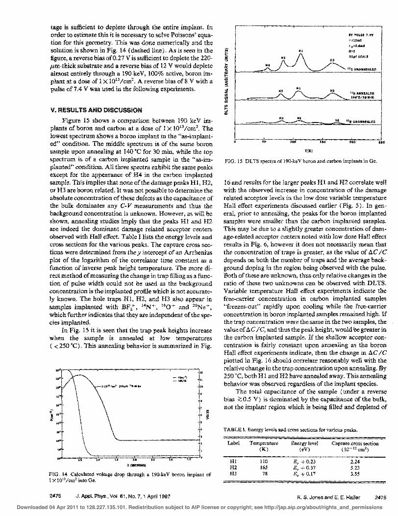
V. RESULTS AND DISCUSSION Figure 15 shows a comparison between 190 keV im-
plants of boron and carbon at a dose of I X 1013 Icm2• The lowest spectrum shows a boron implant in the ed" condition. The middle spectrum is of the same boron sample upon annealing at 140 °C for 30 min, while the top spectrum is of a carbon implanted sample in the planted" condition. All three spectra exhibit the same peaks except for the appearance of H4 in the carbon implanted sample. This implies that none of the damage peaks HI, H2, or H3 are boron related. It was not possible to determine the absolute concentration of these defects as the capacitance of the bulk dominates any C-V measurements and thus the background concentration is unknown. However, as will be shown, annealing studies imply that the peaks HI and H2 are indeed the dominant damage related acceptor centers observed with Hall effect. Table I lists the energy levels and cross sections for the various peaks. The capture cross sec-tions were determined from the y intercept of an Arrhenius plot of the logarithm of the correlator time constant as a function of inverse peak height temperature. The more di-rect method of measuring the change in trap filling as a func-tion of pulse width could not be used as the background concentration is the implanted profile which is not accurate-ly known. The hole traps HI, H2, and H3 also appear in samples implanted with BFt, 14N+, <60+ and 2°Ne+, which further indicates that they are independent of the spe-cies implanted.
In Fig. 15 it is seen that the trap peak heights increase when the sample is annealed at low temperatures ( < 250 CC), This annealing behavior is summarized in Fig.
.. i",.U,I.,ll IHIIQIi t.1tD. ell , .
.. '
\ "5 •• " iii:" ... '
....
.. .• ,o!-_-.* .• FIG. 14. Calculated voltage drop through a 190-keV boron implant of 1 X lOB Icm2 into Ge.
2475 J. Appl. ?hys., Vol. 61, No.7, 1 April 1987
BV 7.4\1 r=iOmS TM=C.GmS
;;; fll Go, l-i ICA!.£ ::lI ,.. II< "c UIIAKKEALED c DO l-ii Ill! 5 ... III C He z " !40-CI30 HIH. &> !II I--' a
M3 HI "I UMAIiNULliI
100 150 2141
T!K)
FIG. 15. DLTS spectra of 190-keV boron and carbon implants in Ge.
16 and results for the larger peaks HI and H2 correlate weU with the observed increase in concentration of the damage related acceptor levels in the low dose variable temperature Hall effect experiments discussed earlier (Fig. 5). In gen-eral, prior to annealing, the peaks for the boron implanted samples were smaller than the carbon implanted samples. This may be due to a slightly greater concentration of age-related acceptor centers noted with low dose Han effect results in Fig. 6, however it does not necessarily mean that the concentration of traps is greater, as the value of IC depends on both the number of traps and the average back-ground doping in the region being observed with the pulse. Both of these are unknown, thus only relative changes in the ratio of these two unknowns can be observed with DL TS. Variable temperature Hall effect experiments indicate the
concentration in carbon implanted samples rapidly upon cooling while the free-carrier
concentration in boron implanted samples remained high. If the trap concentration were the same in the two samples, the value of I::..C Ie, and thus the peak height, would be greater in the carbon implanted sample. If the shallow acceptor centration is fairly constant upon annealing as the boron Hall effect experiments indicate, then the change in Il.C Ie plotted in Fig. 16 should correlate reasonably well with the relati.ve change in the trap concentration upon annealing. By 250°C, both H 1 and H2 have annealed away. This annealing behavior was observed regardless of the implant species.
The total capacitance of the sample (under a reverse bias ::::0.5 V) is dominated by the capacitarr--e of the bulk, not the implant region which is being :filled and depleted of
TABLE I. Energy levels and cross sections for various peaks .
Label Temperature Energy level Capture cross section (K) (eV) (10-<2 cm2 )
Hl 110 E" +0.23 2.24 HZ 165 E. +0.37 5.23 H3 78 E" +0.17 3.55
K. S. Jones and E. E. Haller 2475 Downloaded 04 Apr 2011 to 128.227.135.101. Redistribution subject to AIP license or copyright; see http://jap.aip.org/about/rights_and_permissions

18
181
17
11
15
14
13
12
... 11 (, ;t 10
•
• '1
SO 100
• '" Ey + 0,23 111 • = Iv" 0.31 112 O"Ey+ tU7 113
150 250
ANNEAL TEMP{"C) (30 MINUTES) :too 350
FIG. 16. Relative defect concentration as a function of anneal temperature,
free carriers. The total capacitance change upon pUlsing the voltage (i.e., 8 V rev bias pulsing 7.5 V forward bias) is very small and accordingly the value of !:..C relative to the C of the bulk is also very small. Thus, a small !:..C Ie does not neces-sarily mean a sman trap concentration.
The energy levels and capture cross sections of H 1 and H2 match quite well with two hole traps observed by Pear-ton et at. II They found the same acceptor levels in r-irradiat-ed Ge and concluded they are oxygen-vacancy related com-plexes. To further substantiate the theory that HI and H2 are the same peaks Pearton et al. observed, the annealing characteristics of both sets of peaks are identical.
The hole trap H3 is observed to anneal out between 150-200 ·C. Bourgoin et al. 12 have observed a hole trap with the same depth and similar annealing characteristics, using DLTS to study room temperature electron irradiated n-type germanium. They associate this hole trap and two electron traps with the divacancy.
The preliminary identification of all three hole traps H 1, H2, and H3 is consistent with the observation of the traps being associated with damage induced. species independent levels. Variable temperature Hall effect investigations using implantations of oxygen as well as other species are in prog-ress to help detennine if the major damage related acceptor centers involve oxygen. Sources of oxygen such as "knock-on" oxygen from the surface and oxygen grown into the crystal must be recognized in interpreting the results.
Upon annealing at higher temperatures ( > 300 ·C), Cu peaks were observed to grow confirming our suspicion that Cu contamination was the reason for the substrate conver-
2476 J" Appl. Phys., Vol. 61, No.7. 1 April 1987
sian observed upon high-temperature annealing of VTHE samples.
VI. CONCLUSIONS liB +, 12C+, and BF2+ ions implanted into Ge were
studied using two techniques. Carrier concentration of the implanted layers as a function of implantation species, im-plantation dose, implantation energy, and postimplant an-nealing temperature have been investigated using Hall ef-fect" The characterization of the damage created upon implantation using DLTS was also presented.
The results of the experiments on boron implants indi-cate that over the entire dose range (5X 1O"/cm2 to 1 X 10¹⁴/cm2) and energy range (25-150 keY) studied, 100% of the boron ions are substitutionally active upon im-plantation at room temperature. For low-energy implants (25 keY) of boron the concentration of stable damage relat-ed acceptor centers is significantly less than the concentra-tion of shallow boron related acceptor centers over the entire dose range studied< As the implantation energy increases the concentration of damage related acceptor centers per incom-ing ion also increases. This increase in damage is more signif-icant at lower doses than at higher doses. Thus, at 100 keY, the concentration of damage related acceptor centers be-comes greater than the concentration of shallow boron ed acceptor centers at doses below 1 X 10¹²/cm2•
The damage related acceptor centers consist of three hole traps, HI, H2, and H3. None ofthese traps are associat-ed with boron. Upon annealing below 225°C the concentra-tion of HI and H2 appears to increase. Annealing for 30 min at temperatures above 250°C results in the elimination ofH 1 and H2. Hole trap H3 is annealed away after 30 min at 150°C. The hole traps HI and H2 have been observed before by Pearton et al. II in D L TS studies on r-irradiated Ge" They concluded these are oxygen-vacancy related defects. H3 ap-pears to be the same hole trap observed by Bourgoin et al. 12
in electron irradiated Ge. They suggested that it may be asso-ciated with a divacancy.
The boron in BF2 implants is not electrically active upon room-temperature implantation within the dose range and energy range discussed above. The same three hole traps, HI, H2, and H3, are observed" Upon annealing at 350·C for 30 min the damage is repaired and the boron is substitution-al.
ACKNOWLEDGMENTS The authors would like to thank Dr. Nancy Haegel for
the many helpful discussions and Dick Chan for doing all of the implantations. This work was supported in part by the National Science Foundation, Grant DMR-8203430 and in part by the Director's Office of Energy Research, Office of Health and Environmental Research, U.S. Department of Energy under Contract No. DE-AC03-76SF00098"
lJ. P. Ponpon. J" J. Grob, R. Stuck. P. Burger, and P. Siffert, Second Inter-national Conference on Ion Implantation, Garmish (Springer, Berlin, 1972).
20. D" Alton and L. O. Love, Can. J. Phys. 46, 695 (1968).
K. S. Jones and E. E. Haller 2476
Downloaded 04 Apr 2011 to 128.227.135.101. Redistribution subject to AIP license or copyright; see http://jap.aip.org/about/rights_and_permissions

3Ho Herzer and So Kalbitzer, Second International Conference on Ion Im-plantation, Garmish (Springer, Berlin, 1972)0
4G. Do Alton, Isotope Division, Oak Ridge Nat. Lah Report, August (l96n
'Do Sigurd. G, Fladda, L Eriksson, and K Bjorkqvist, Radiato El[ 3,145 (1970),
6L J. Vall derPauw, Philips Res. Rep. 13, 1 (1958). 7J. F. Gibbons, W. S. Johnsoll, and S. W, Mylroie, Projected RangeStatis-
2477 J. Appl. Phys., Vol. 61, No.7, 1 April 1987
tics (Halstead, Stroudsberg, PA, 1975). 8V. I. Fistul', Heavily Doped Semiconductors (Plenum, New York, 1969). 9R. L Petritz R L, Phys. Rev. 110, 1254 (1958). IOD. V. Lang, J. App!. Phys, 45, 3023 (1974). j 's. J. Pearton, A. J. Tavendale, J. M. Kahn, and E. E. Haller, Radiat. Elf.
81,293 (1984). 12J, C. Bourgoin, P. M. Mooney, and F. Poulin, International Conjerenceofl
Defects and Radiation Effects in Semiconductors (Oiso, Japan, 1980).
K. S. Jones and E. E. Haller 2477
Downloaded 04 Apr 2011 to 128.227.135.101. Redistribution subject to AIP license or copyright; see http://jap.aip.org/about/rights_and_permissions