Embed Size (px)
Citation preview
1AE0B36APO Computer Architectures
Computer Architectures
I/O subsystem 2
Michal Štepanovský, Pavel Píša, Miroslav Šnorek
Czech Technical University in Prague, Faculty of Electrical Engineering
Ver.1.10

2AE0B36APO Computer Architectures
Lecture outline
● I/O subsystem – final part● Memory mapped I/O● PCI as seen by PC system● PCI device controller
● Secondary memory – disk● Speedup and reliability● RAID – Redundant Array of
Inexpensive/Independent Disks
3AE0B36APO Computer Architectures
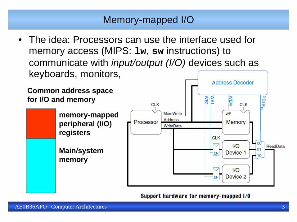
Memory-mapped I/O
● The idea: Processors can use the interface used for memory access (MIPS: lw, sw instructions) to communicate with input/output (I/O) devices such as keyboards, monitors, and printers.
Common address space for I/O and memory
memory-mapped peripheral (I/O) registers
Main/system memory
4AE0B36APO Computer Architectures
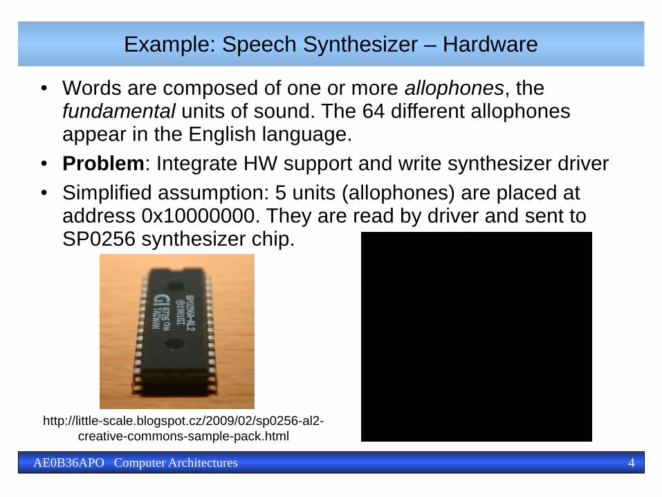
Example: Speech Synthesizer – Hardware
● Words are composed of one or more allophones, the fundamental units of sound. The 64 different allophones appear in the English language.
● Problem: Integrate HW support and write synthesizer driver● Simplified assumption: 5 units (allophones) are placed at
address 0x10000000. They are read by driver and sent to SP0256 synthesizer chip.
http://little-scale.blogspot.cz/2009/02/sp0256-al2-creative-commons-sample-pack.html
5AE0B36APO Computer Architectures
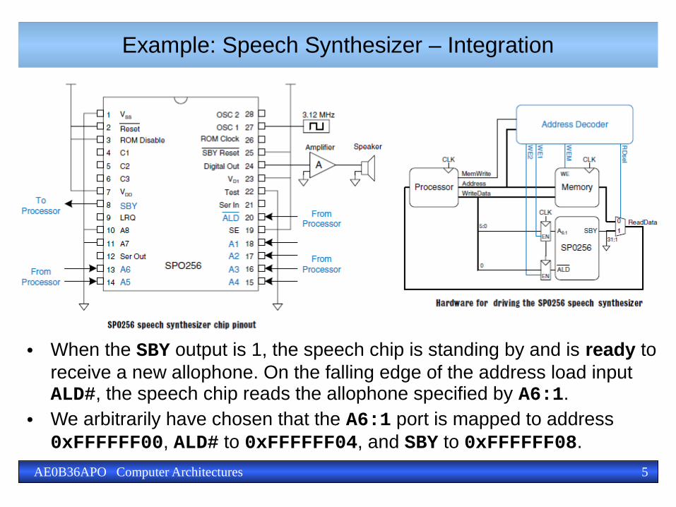
Example: Speech Synthesizer – Integration
● When the SBY output is 1, the speech chip is standing by and is ready to receive a new allophone. On the falling edge of the address load input ALD#, the speech chip reads the allophone specified by A6:1.
● We arbitrarily have chosen that the A6:1 port is mapped to address 0xFFFFFF00, ALD# to 0xFFFFFF04, and SBY to 0xFFFFFF08.
6AE0B36APO Computer Architectures
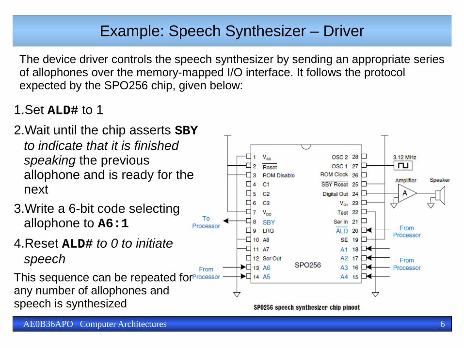
The device driver controls the speech synthesizer by sending an appropriate series of allophones over the memory-mapped I/O interface. It follows the protocol expected by the SPO256 chip, given below:
Example: Speech Synthesizer – Driver
1.Set ALD# to 1
2.Wait until the chip asserts SBY to indicate that it is finished speaking the previous allophone and is ready for the next
3.Write a 6-bit code selecting allophone to A6:1
4.Reset ALD# to 0 to initiate speech
This sequence can be repeated for any number of allophones and speech is synthesized
7AE0B36APO Computer Architectures
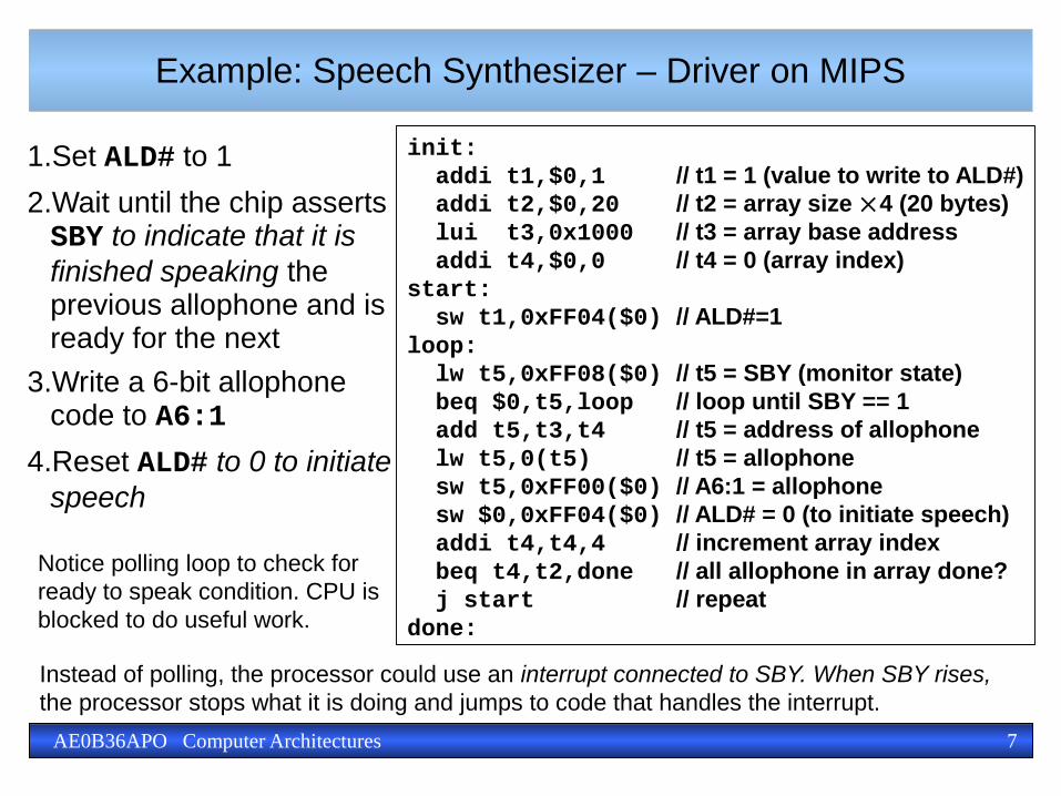
Example: Speech Synthesizer – Driver on MIPS
1.Set ALD# to 1
2.Wait until the chip asserts SBY to indicate that it is finished speaking the previous allophone and is ready for the next
3.Write a 6-bit allophone code to A6:1
4.Reset ALD# to 0 to initiate speech
init: addi t1,$0,1 // t1 = 1 (value to write to ALD#) addi t2,$0,20 // t2 = array size ×4 (20 bytes) lui t3,0x1000 // t3 = array base address addi t4,$0,0 // t4 = 0 (array index)start: sw t1,0xFF04($0) // ALD#=1loop: lw t5,0xFF08($0) // t5 = SBY (monitor state) beq $0,t5,loop // loop until SBY == 1 add t5,t3,t4 // t5 = address of allophone lw t5,0(t5) // t5 = allophone sw t5,0xFF00($0) // A6:1 = allophone sw $0,0xFF04($0) // ALD# = 0 (to initiate speech) addi t4,t4,4 // increment array index beq t4,t2,done // all allophone in array done? j start // repeatdone:
Instead of polling, the processor could use an interrupt connected to SBY. When SBY rises, the processor stops what it is doing and jumps to code that handles the interrupt.
Notice polling loop to check for ready to speak condition. CPU is blocked to do useful work.

8AE0B36APO Computer Architectures
Generalized summary based on example
● There are two methods for I/O devices (peripherals) access● memory mapped I/O● I/O specialized instructions (if implemented/available) – they use address
space independent of memory access● There are address range(s) dedicated to device access in the case of
memory mapped I/O. Reads/writes from/to these addresses are interpreted as commands or data transfers from/to peripheral devices. Memory subsystem is informed about I/O ranges and ignores these accesses. I/O devices/bus controller is aware of addresses assigned to it and fulfills requests.
● The CPU can be informed about I/O device request for service by:● repeated monitoring of its ready condition (status register) – polling ● interrupt request – interrupt-driven I/O – it is asynchronous to the actual
program execution (is initiated by device when it needs servicing)● Have you noticed address decoder function?● What about caches in the case of I/O range/region access?

9AE0B36APO Computer Architectures
PCI Continued

10AE0B36APO Computer Architectures
Some points from last lecture to remember
PCIdevice
INTA#
INTB#
INTC#
INTD#
AD[31::00]
C/BE[3::0]#
FRAME#
TRDY#
IRDY#
STOP#
DEVSEL#
IDSEL#
PERR#
SERR#
REQ#
GNT#
CLK#
RST#
addressand data
PAR
interfacecontrol
errorreporting
accessarbitration
(master only)
system
There will be test during week 9
Memory read timing
Why is sending byte bit-by-bit (serial) is faster? Signal interferences, differential signaling, clock skew and different paths lengths, reflection and common voltage.

11AE0B36APO Computer Architectures
PCI devices examples

12AE0B36APO Computer Architectures
Computer startup procedure (from PCI perspective)
1. CPU is directed by BIOS code to retrieve device identification for each PCI slot. This is done by read cycle from PCI configuration space. The read (topological) address decodes to IDSEL (Initialization Device Select) signal to the corresponding PCI slot (bus/device/function) + register number
2. Each device identification (Vendor ID, Device ID) and request for I/O resources (sizes of I/O ports and memory ranges and interrupt link (A/B/C/D) use by function) are read. All this information is available in card/slot configuration space. This search is done together with bus numbers assignment when bridge is found.
3. BIOS allocates non-overlapping ranges to the devices. It ensures that there is no collision with system memory and I/O. Interrupts can be, and are, shared but sharing level can be balanced. Allocated ranges/resources are written to the corresponding device/function Base Address Register (BAR). They usually stay constant till computer power off but OS can reconfigure them under certain circumstances.
4. Operating System is loaded and given control. OS reads devices identifications again from PCI configuration space and locates device drivers according to VID:PID (+class,+subsystem IDs).
● This process of device “searching” is called enumeration and is used in some form by each PnP aware bus (PCI, USB, etc.).

13AE0B36APO Computer Architectures
PCI bus hierarchy
DI D2
1
BridgeDI D2
DI
DI D2
CPU
Bus 0
Bus 1
Bridge Bridge
3 2
Bus 4
Bridge
4
Bus 2Bus 3
Subordinate=4
Primary Bus = 0Secondary Bus = 1
Subordinate=2
Primary Bus = 1Secondary Bus = 2
Subordinate=4
Subordinate=4
Primary Bus = 1Secondary Bus = 3
Primary Bus = 3Secondary Bus = 4

14AE0B36APO Computer Architectures
PCI BUS address space(s)
● PCI bus recognizes three address spaces:● memory – address is 32 or 64-bit● I/O – exists mainly for compatibility with x86 specific I/O ports and
I/O instructions concept● configuration space – 256 bytes are assigned to each device
function in the basic PCI bus variant, 8 functions per device/slot/card and 32 devices per bus can exist in maximum.
● Each end-point device can implement up to 6 Base Address Registers (BARs) which can define up to 6 independent regions (address ranges) – each for I/O or memory mapped access. For 64-bit ranges BARs are used in pairs. The requested size is obtained by writing ones into BAR bits and reading back where BAR's bits corresponding to the range size are fixed on zero. LSB bits then informs about address space type. Then BIOS/OS writes allocated region start address back to the BAR.
15AE0B36APO Computer Architectures
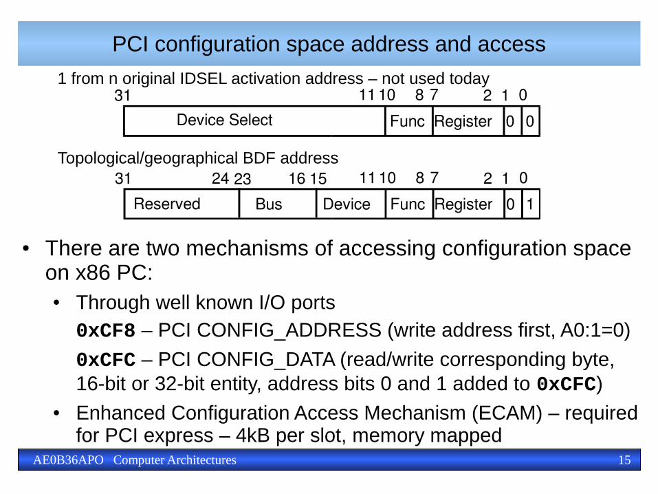
PCI configuration space address and access
● There are two mechanisms of accessing configuration space on x86 PC:
● Through well known I/O ports0xCF8 – PCI CONFIG_ADDRESS (write address first, A0:1=0)
0xCFC – PCI CONFIG_DATA (read/write corresponding byte, 16-bit or 32-bit entity, address bits 0 and 1 added to 0xCFC)
● Enhanced Configuration Access Mechanism (ECAM) – required for PCI express – 4kB per slot, memory mapped
071131 10 8 2 1
00Func RegisterDevice Select
071131 10 8 2 1
0Func Register 1Reserved DeviceBus
24 23 16 15Topological/geographical BDF address
1 from n original IDSEL activation address – not used today
16AE0B36APO Computer Architectures
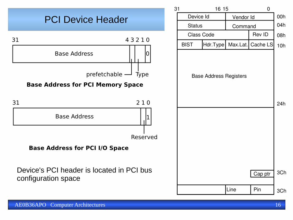
PCI Device Header31 1516 0
Device Id Vendor Id
CommandStatus
Class Code
00h
04h
08h
24h
10h
3Ch
Base Address Registers
Line Pin
Rev ID
BIST Hdr.Type Max.Lat. Cache LS
3ChCap ptr
0131
Reserved
Base Address 1
Base Address for PCI I/O Space
2
234
Base Address
Typeprefetchable
Base Address for PCI Memory Space
01
0
31
Device's PCI header is located in PCI bus configuration space

17AE0B36APO Computer Architectures
PCI Device Header Type 0 – End-point device
Device ID Vendor ID
Status Command
Class Code Revision ID
BIST Header Type Master Lat. Timer Cache Line Size
Base Address Registers6 max
Cardbus CIS Pointer
Subsystem ID Subsystem vendor ID
Expansion ROM Base Address
Reserved Capabilities Pointer
Reserved
Max_Lat Min_Gnt Interrupt Pin Interrupt Line
ByteOffset
00h
04h
08h
0Ch
10h
14h
18h
1Ch
20h
24h
28h
2Ch
30h
34h
38h
3Ch

18AE0B36APO Computer Architectures
PCI Device Header Type 1 – Bus BridgesByteOffset
00h
04h
08h
0Ch
10h
14h
18h
1Ch
20h
24h
28h
2Ch
30h
34h
38h
3Ch
Reserved Capabilities Pointer
Expansion ROM Base Address
Bridge Control Interrupt Pin Interrupt Line
Device ID Vendor ID
Status Command
Class Code Revision ID
BIST Header Type Master Lat. Timer Cache Line Size
Base Address Register 0
Base Address Register 1
Secondary LatencyTimer
Subordinate BusNumber
Secondary BusNumber
Primary BusNumber
Secondary Status I/O Limit I/O Base
Prefetchable Memory Limit Prefetchable Memory Base
Prefetchable Base Upper 32 Bits
Prefetchable Limit Upper 32 Bits
I/O Limit Upper 16 Bits I/O Limit Base Upper 16 Bits
Memory Limit Memory Base

19AE0B36APO Computer Architectures
I/O address space (x86 in, out instructions)
BAR 0BAR 1BAR 2BAR 3BAR 4BAR 5
Mem
I/O
Mem
Memory space: common for I/O and system memory
BAR 0BAR 1BAR 2BAR 3BAR 4BAR 5 Mem
PCI card #0
PCI card #1
If CPU writes to this location, write is recognized by PCI device/card #0. Its effect depends on card logic. I.e. for graphic card frame-buffer it behaves same as regular memory, but data are seen on the screen.
Mem
I/O
Memory
PCI device/card is informed about assigned addresses …
BAR registry
datadatadata
data
datadata

20AE0B36APO Computer Architectures
I/O address space (x86 in, out instructions)
BAR 0BAR 1BAR 2BAR 3BAR 4BAR 5
Mem
I/O
Mem
Memory space: common for I/O and system memory
BAR 0BAR 1BAR 2BAR 3BAR 4BAR 5 Mem
PCI card #0
PCI card #1
If CPU writes to this location, write is recognized by PCI device/card #0. Its effect depends on card logic…
Mem
I/O
Memory
PCI device/card is informed about assigned addresses …
BAR registry
datadatadata
data
datadata
This is physical
/bus address
Study mmap() function manual.
Do not forget to munmap()…
mmap(BAR1)
base addr. +4mmap(BAR0)
mmap(BAR1)
CPU/code use virtual
addresses and are translated
by MMU !!!

21AE0B36APO Computer Architectures
Linux /proc/bus/pci directory
● Each directory represents one PCI bus (with its number assigned) and each file mirrors one PCI device function PCI header (the first 64 bytes)
● Homework: Write C/C++ language program that can traverse and open files in given directory and its subdirectory and searches for given sequence of four characters (4B) at each file start. The full path of the first matching file is printed.

22AE0B36APO Computer Architectures
Linux /proc/bus/pci directory – command lspci -vb
00:00.0 Host bridge: Intel Corporation 82X38/X48 Express DRAM Controller Subsystem: Hewlett-Packard Company Device 1308 Flags: bus master, fast devsel, latency 0 Capabilities: [e0] Vendor Specific Information <?> Kernel driver in use: x38_edac Kernel modules: x38_edac
00:01.0 PCI bridge: Intel Corporation 82X38/X48 Express Host-Primary PCI Express Bridge Flags: bus master, fast devsel, latency 0 Bus: primary=00, secondary=01, subordinate=01, sec-latency=0 I/O behind bridge: 00001000-00001fff Memory behind bridge: f0000000-f2ffffff Kernel driver in use: pcieport Kernel modules: shpchp
00:1a.0 USB Controller: Intel Corporation 82801I (ICH9 Family) USB UHCI Controller #4 (rev 02) Subsystem: Hewlett-Packard Company Device 1308 Flags: bus master, medium devsel, latency 0, IRQ 5 I/O ports at 2100 Capabilities: [50] PCI Advanced Features Kernel driver in use: uhci_hcd

23AE0B36APO Computer Architectures
PCI Device Card Interface Design Example
● The card requires three address ranges● Two memory mapped, 4kiB each● One I/O space mapped, size 16B
● Dezign steps● Analyze bus cycles sequences that should be recognized● Remember electronics (CPU, bus) building blocks● Define interface structure● Implement address decoder● Implement control logic● Implement data path● And then think what the card should be used for
– NO, regular design starts from function and its needs
24AE0B36APO Computer Architectures
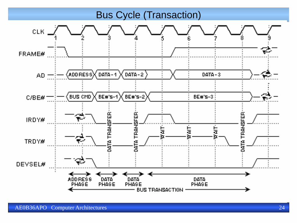
Bus Cycle (Transaction)

25AE0B36APO Computer Architectures
Interface Building Blocks
● Data bus and block to control datapath (enable, direction)
● Address signals, address decoder● Command decoder● Control logic● (Interrupt signal generator – INT#)
● Only when card uses interrupt – but highly desirable
● Logic to request bus control (initiator/master) role from the bus arbiter● Only if card is/can act as master (bus master DMA
etc.)

26AE0B36APO Computer Architectures
PCI Device/Card Interface
data
Address decoder32 bits
Datapaths control
ADBAR addr
C/BE# Commanddecoder4 bity
Control logic
FRAME#
TRDY#
IRDY#and more
reg index/addr

27AE0B36APO Computer Architectures
Address Decoder
● The basic block is address comparator● It compares significant bits (according to the region size) of
the address sent on bus with the address stored in one of the base address registers (one comparator for each BAR)
● Address is present on AD signals only in the first phase of the bus cycle ⇒ the address has to be latched (stored) in card's address register
● If block transfers are supported then address register has to provide autoincrement function – it is realized by up counter with parallel preset (LOAD)
● Consider relocable address decoder. Consider reduced comparator – mirroring.
28AE0B36APO Computer Architectures
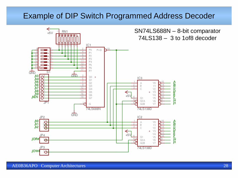
Example of DIP Switch Programmed Address Decoder
SN74LS688N – 8-bit comparator74LS138 – 3 to 1of8 decoder

29AE0B36APO Computer Architectures
Configurable Address Decoder (i.e. BAR Based)
Addressregister
COMP_MEM1KOMP_MEM2COMP_I/O
32 bits
20 bits
Config.registers
20 bits28 bitsA[31:4]
LOADINC1INC4
I/O rangeselectedADDRIO
ADDRMEM
12 bitsA[11:0]to internallogic
AD[1:0]
A[31:12]
AD[31:0]

30AE0B36APO Computer Architectures
Configurable Address Decoder Signals
● ADDRIO● Address matches I/O range
● ADDRMEM● Address matches one of two memory mapped ranges
● Address register is a synchronous counter with parallel synchronous preset
● LOAD – synchronous address load on the next rising edge of the clocks
● INC1 – increment stored value/address by 1● INT4 – increment stored value/address by 4
● AD[1:0] – informs internal logic about burst mode type

31AE0B36APO Computer Architectures
Other Required Blocks
● Configuration space● Register array (size 256B). All cells can be read, writes to
some registers/bits are ignored (i.e. BAR's low order bits)● Parity check (generates PERR# signal)● Error control, i.e. check for the address register/counter
overflow during continuous/burst transfer (generates SERR# signal)
● Consider wait cycles logic TRDY# assignment etc.● Address for memory reads/writes has to be 4 bytes aligned
(partial bus use/data validity can be controlled by C/BE[3:0] signals) ⇒ address increment is 4 for memory accesses
● but for I/O byte wide accesses INC1 required as well

32AE0B36APO Computer Architectures
Datapaths and their Control
● Data bus is bidirectional the interface requires ⇒(bidirectional) transceiver with three-state outputs
● 8/16/32-bit data transfers the direction and the high impedance state control is based on command type (read/write) and on mask selecting valid octets of bits on the bus C/BE#
33AE0B36APO Computer Architectures
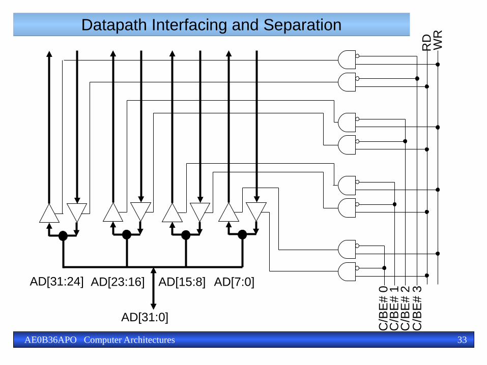
Datapath Interfacing and Separation
AD[31:0]
AD[31:24] AD[23:16] AD[15:8] AD[7:0]
C/B
E#
3C
/BE
# 2
C/B
E#
1C
/BE
# 0
RD
WR

34AE0B36APO Computer Architectures
Pre-PCI Style I/O Port Realization Example
74LS244N - Edge Triggered Flip-Flop74LS245N - Octal Bus Transceiver with 3-State Outputs

35AE0B36APO Computer Architectures
PCI Command Decoder
● Command is latched into command register● Command decoder is then realized as combinatorial logic● Outputs are control signals which specify:
● data transaction direction● transaction type
I/O operation, memory space operation, configuration access/cycle, interrupt request/acknowledge
● Use of combinatorial decoder simplifies control logic design● Compare with opcodes decode and arithmetic operation
specifications described in lecture “Processor”

36AE0B36APO Computer Architectures
Command Decoder
Commandregister
C/BE[3:0]#
LOAD_CMD
Commanddecoder

37AE0B36APO Computer Architectures
Command Decode – C/BE[3..0]# Meaning
C/BE[0::3]# Bus command (BUS CMD)
0000 Interrupt Acknowledge
0001 Special Cycle
0010 I/O Read
0011 I/O Write
0100 Reserved
0101 Reserved
0110 Memory Read
0111 Memory Write
1000 Reserved
1001 Reserved
1010 Configuration Read (only 11 low addr bits for fnc and reg + IDSEL)
1011 Configuration Write (only 11 low addr bits for fnc and reg + IDSEL)
1100 Memory Read Multiple
1101 Dual Address Cycle (more than 32 bits for address – i.e. 64-bit)
1110 Memory Read Line
1111 Memory Write and Invalidate

38AE0B36APO Computer Architectures
Command Decoder Output Signals
● RD – read operation● WR – write operation● IO – operation targets I/O space● MEM – operation targets memory space● CONF – read/write from/to configuration space● INT – command Interrupt Acknowledge

39AE0B36APO Computer Architectures
Interface Control
● Detect start and end of a cycle● Generates DEVSEL# if address recognized by
device/card, controls address register, command register and decoder, monitors IRDY# signal (wait cycle inserted by initiator – master) to inform card logic that given transaction phase is prolonged
● Input signals are● FRAME# – controls transaction start and transaction last
transfer phase● IRDY# – initiator ready/wait request● ADDRIO, ADDRMEM, MEM, IO

40AE0B36APO Computer Architectures
Interface Control Realization
● Sequential circuit can be described/realized as finite state machine
● PCI clock signal is used as clock input for designed FSM, synchronous bus and control design
● Quiz:● Should be design based on Moore FSM or Meally FSM or
it is not important?

41AE0B36APO Computer Architectures
Quiz Answer
● The control logic design has to be Meally FSM, because control signals have to be prepared even before first rising clock of the PCI clock to select the right function of address latch register and other components
● Design choice● We consider all control signals in positive logic for
simplicity

42AE0B36APO Computer Architectures
Interface Controller/FSM Signals
● Output signals● LOAD● LOAD_CMD● DEVSEL#● VALID_TRANS● INC1, INC4, PAUSE (wait/phase hold for internal logic)
● Design choices● only active output signals are shown in the transition graph● ADDRESS = ((ADDRIO==1 and IO==1) or (ADDRMEM==1
and MEM==1))

43AE0B36APO Computer Architectures
PCI Interface FSM
Q0
Q1
FRAME# = 1FRAME# = 0 / LOAD=1,LOAD_CMD=1
FRAME# = 1 and ADDRES=1 /DEVSEL# = 0, VALID_TRANS=1
Q3
FRAME# = 1
FRAME# = 0
FRAME# = 0and ADDRESS=0
IRDY# = 1 /PAUSE = 1
Q2
FRAME# = 0 and ADDRMEM=1 andMEM=1 / DEVSEL# = 0,VALID_TRANS=1, INC4=1
IRDY# = 1 / PAUSE = 1,VALID_TRANS = 1
FRAME# = 0, ADDRIO=1 /INC = 1,VALID_TRANS=1
FRAME# = 0, ARDMEM = 1 /INC4 = 1, VALID_TRANS=1
FRAME# = 1 /VALID_TRANS=1
FRAME# = 0 a ADDRIO=1 andIO=1/ DEVSEL# = 0,VALID_TRANS=1, INC=1
FRAME# = 1 and ADDRESS=0

44AE0B36APO Computer Architectures
Data Path Direction and HiZ Control
● The data path transceiver direction and high impedance state control can be derived from signals
● VALID_TRANS and WR● VALID_TRANS and RD
generated by command decoder

45AE0B36APO Computer Architectures
Disk – Another Critical Memory Hierarchy Component
● Enhancement required● Speedup● Reliability
46AE0B36APO Computer Architectures
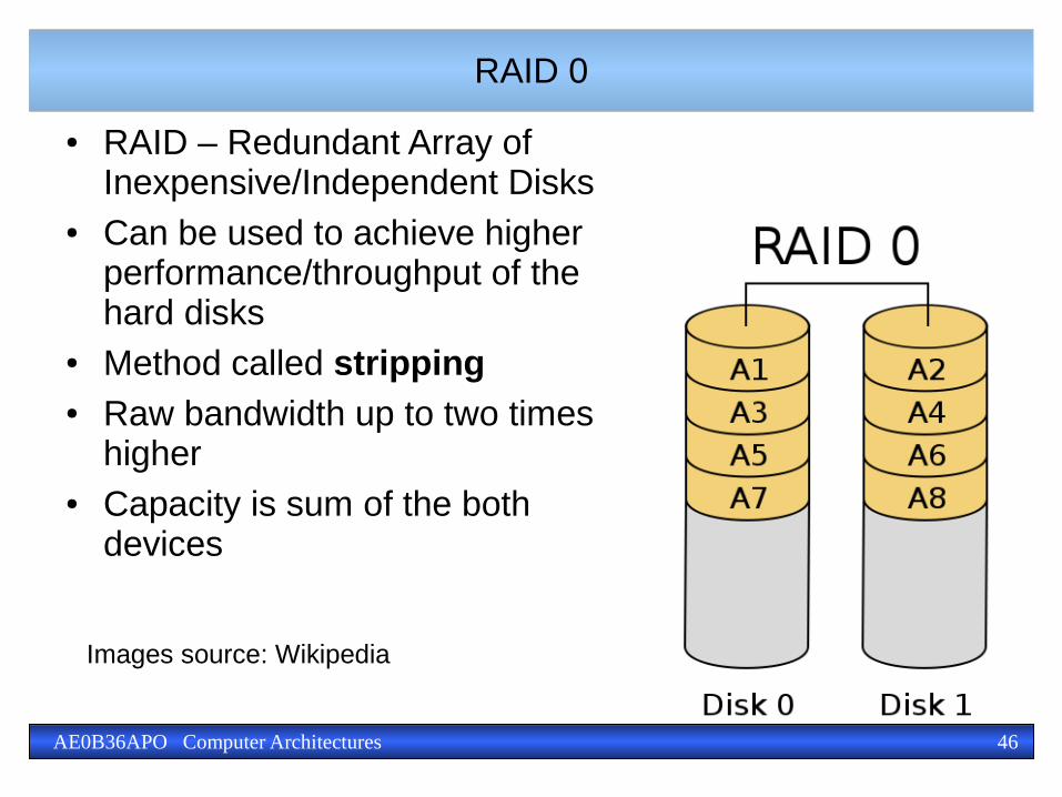
RAID 0
● RAID – Redundant Array of Inexpensive/Independent Disks
● Can be used to achieve higher performance/throughput of the hard disks
● Method called stripping● Raw bandwidth up to two times
higher● Capacity is sum of the both
devices
Images source: Wikipedia

47AE0B36APO Computer Architectures
RAID 1
● Each data block exists in two copies, each on one of two independent disks
● The total capacity is same as of a single disk
● Data reliability is much higher, probability of coincidence of two independent events (disk failures) is much much lower than for single device
● Method is called mirroring● Write has some overhead against
single device. Reads can be optimized for less head movement

48AE0B36APO Computer Architectures
RAID 10
● It is combination of both previous techniques● RAID 0 is created first on two (or more) devices and all
data are copied on the second set of devices (same as for RAID1)
● RAID 10 contributes to both – reliability and performance● Disadvantage – at least 4 drives with same capacity are
required.● Total capacity T, disk capacity D, number of drives n
n=2⋅ceil( T2⋅D )RAID 0 n=2⋅ceil T
D RAID 1
n=4⋅ceil( T2⋅D )RAID 10
49AE0B36APO Computer Architectures
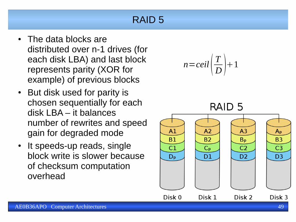
RAID 5
● The data blocks are distributed over n-1 drives (for each disk LBA) and last block represents parity (XOR for example) of previous blocks
● But disk used for parity is chosen sequentially for each disk LBA – it balances number of rewrites and speed gain for degraded mode
● It speeds-up reads, single block write is slower because of checksum computation overhead
n=ceil TD 1

50AE0B36APO Computer Architectures
RAID 6
● Uses two parity blocks on different disks for given disk LBA. Each parity is computed different way.
● It is resistant to two concurrent disk failures
● The read is speed similar to RAID 5, write is more demanding/complex
n=ceil TD 2