Embed Size (px)
Citation preview

Customer Training
Building Gigabit Interfaces in Altera Transceiver Devices
A-MNL-BGIATD-12-0-v1

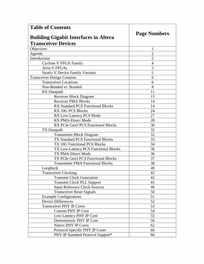
Table of Contents
Building Gigabit Interfaces in Altera Transceiver Devices
Page Numbers
Objectives 1 Agenda 2 Introduction 2
Cyclone V FPGA Family 4 Arria V FPGAs 5 Stratix V Device Family Variants 5
Transceiver Design Creation 6 Transceiver Locations 6 Non-Bonded vs. Bonded 8 RX Datapath 11
Receiver Block Diagram 13 Receiver PMA Blocks 14 RX Standard PCS Functional Blocks 14 RX 10G PCS Blocks 24 RX Low-Latency PCS Mode 27 RX PMA-Direct Mode 28 RX PCIe Gen3 PCS Functional Blocks 30
TX Datapath 32 Transmitter Block Diagram 32 TX Standard PCS Functional Blocks 33 TX 10G Functional PCS Blocks 34 TX Low-Latency PCS Functional Blocks 36 TX PMA-Direct Mode 36 TX PCIe Gen3 PCS Functional Blocks 37 Transmitter PMA Functional Blocks 38
Loopback 40 Transceiver Clocking 42
Transmit Clock Generation 42 Transmit Clock PLL Support 43 Input Reference Clock Sources 46 Transceiver Reset Signals 50
Example Configurations 51 Device Differences 52 Transceiver PHY IP Cores 53
Custom PHY IP Core 54 Low Latency PHY IP Core 55 Deterministic PHY IP Core 56 Native PHY IP Cores 62 Protocol-Specific PHY IP Cores 66 PHY IP Standard Protocol Support* 66
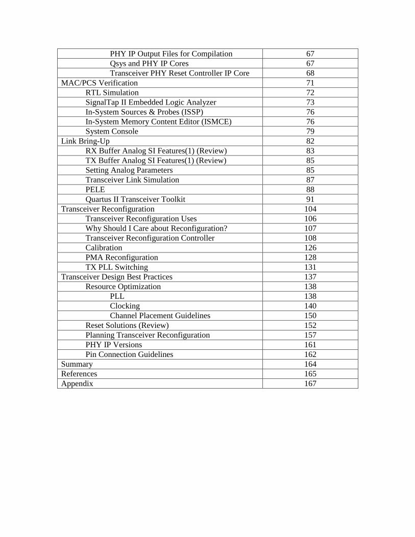
PHY IP Output Files for Compilation 67 Qsys and PHY IP Cores 67 Transceiver PHY Reset Controller IP Core 68
MAC/PCS Verification 71 RTL Simulation 72 SignalTap II Embedded Logic Analyzer 73 In-System Sources & Probes (ISSP) 76 In-System Memory Content Editor (ISMCE) 76 System Console 79
Link Bring-Up 82 RX Buffer Analog SI Features(1) (Review) 83 TX Buffer Analog SI Features(1) (Review) 85 Setting Analog Parameters 85 Transceiver Link Simulation 87 PELE 88 Quartus II Transceiver Toolkit 91
Transceiver Reconfiguration 104 Transceiver Reconfiguration Uses 106 Why Should I Care about Reconfiguration? 107 Transceiver Reconfiguration Controller 108 Calibration 126 PMA Reconfiguration 128 TX PLL Switching 131
Transceiver Design Best Practices 137 Resource Optimization 138
PLL 138 Clocking 140 Channel Placement Guidelines 150
Reset Solutions (Review) 152 Planning Transceiver Reconfiguration 157 PHY IP Versions 161 Pin Connection Guidelines 162
Summary 164 References 165 Appendix 167
Building Gigabit Interfaces inBuilding Gigabit Interfaces in Altera Transceiver Devices
© 2012 Altera Corporation—Confidential
Objectives
Implement high-speed serial protocols in Altera® 28-nm embedded transceiversnm embedded transceivers
Debug transceiver design logic in-system using Altera toolsAltera tools
Optimize analog settings to improve link behavior using Altera toolsusing Altera tools
Employ transceiver reconfiguration to dynamically change transceiver behavior in-systemg y
Improve transceiver usage and avoid transceiver design issues by applying an understanding of device architecture to design situations
© 2012 Altera Corporation—Confidential
2
Building Gigabit Interfaces in Altera Transceiver Devices
A-MNL-BGIATD-12-0-v1 1
Agenda
Transceiver Design Creation
MAC/PCS Verification
Link Bring-Up Link Bring Up
Transceiver Reconfiguration
T i D i B t P ti Transceiver Design Best Practices
© 2012 Altera Corporation—Confidential
3
Building Gigabit Interfaces inBuilding Gigabit Interfaces in Altera Transceiver DevicesI t d tiIntroduction
© 2012 Altera Corporation—Confidential
Building Gigabit Interfaces in Altera Transceiver Devices
A-MNL-BGIATD-12-0-v1 2
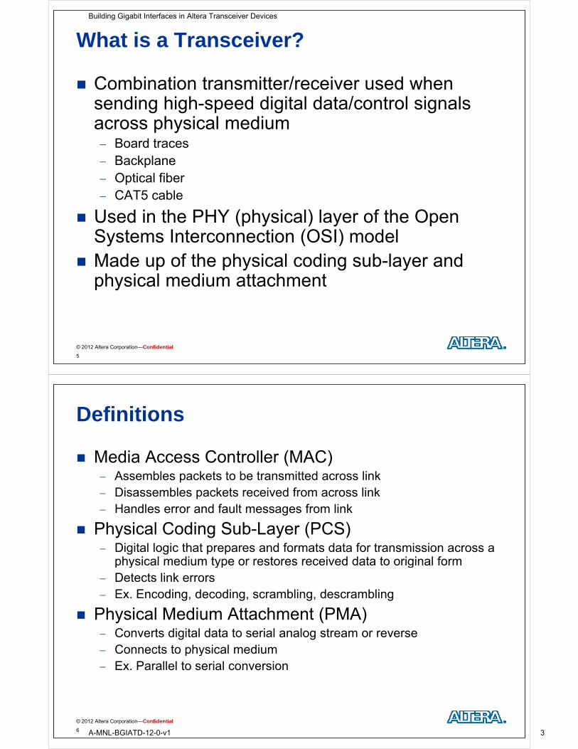
What is a Transceiver?
Combination transmitter/receiver used when di hi h d di it l d t / t l i lsending high-speed digital data/control signals
across physical mediumBoard traces Board traces
Backplane Optical fiber CAT5 cable
Used in the PHY (physical) layer of the Open S t I t ti (OSI) d lSystems Interconnection (OSI) model
Made up of the physical coding sub-layer and h i l di tt h tphysical medium attachment
© 2012 Altera Corporation—Confidential
5
Definitions
Media Access Controller (MAC)A bl k t t b t itt d li k Assembles packets to be transmitted across link
Disassembles packets received from across link Handles error and fault messages from link
Physical Coding Sub-Layer (PCS) Digital logic that prepares and formats data for transmission across a
physical medium type or restores received data to original formphysical medium type or restores received data to original form Detects link errors Ex. Encoding, decoding, scrambling, descrambling
Physical Medium Attachment (PMA) Converts digital data to serial analog stream or reverse
Connects to physical medium Connects to physical medium Ex. Parallel to serial conversion
© 2012 Altera Corporation—Confidential
6
Building Gigabit Interfaces in Altera Transceiver Devices
A-MNL-BGIATD-12-0-v1 3
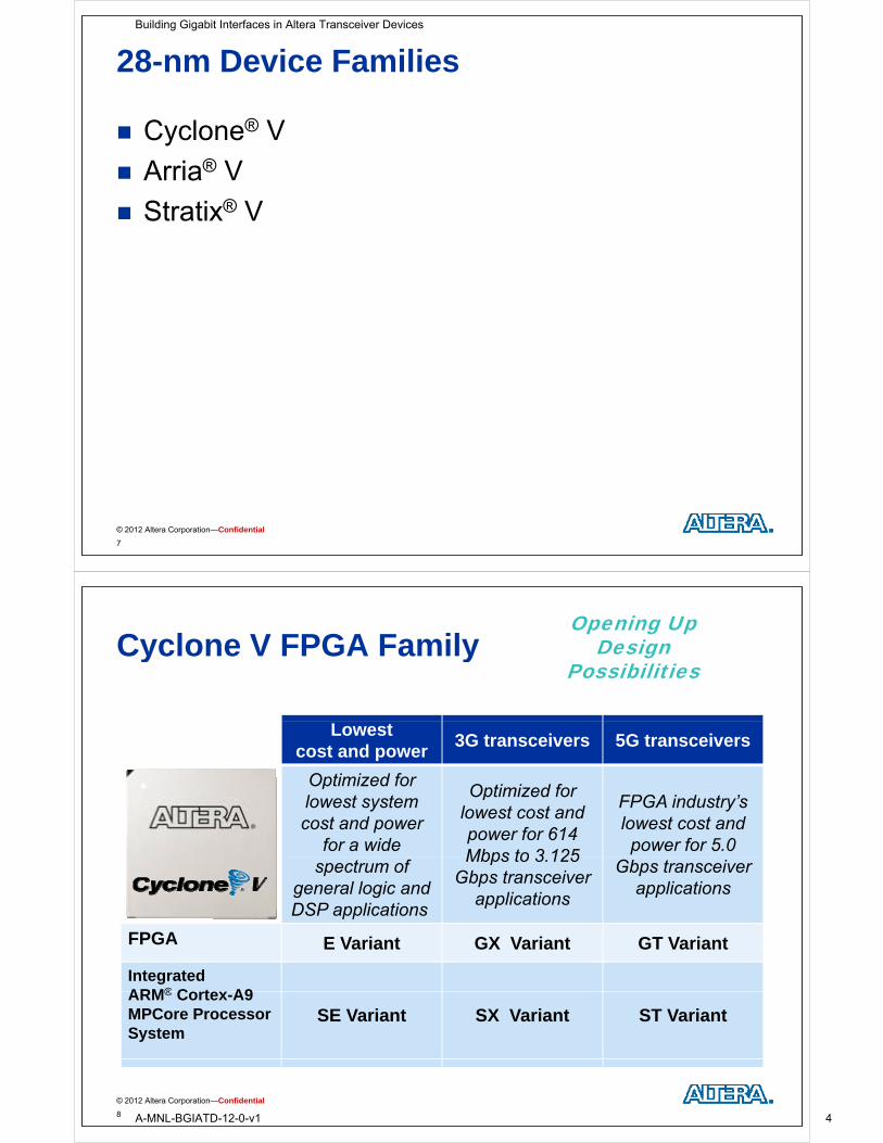
28-nm Device Families
Cyclone® V
Arria® V
Stratix® V Stratix V
© 2012 Altera Corporation—Confidential
7
Cyclone V FPGA FamilyOpening Up
Design Cyclone V FPGA Family es gPossibilities
Lowest cost and power
3G transceivers 5G transceivers
Optimized for Optimized for
plowest system cost and power
for a wide
Optimized for lowest cost and power for 614 Mbps to 3 125
FPGA industry’s lowest cost and power for 5.0
spectrum of general logic and DSP applications
Mbps to 3.125 Gbps transceiver
applications
Gbps transceiver applications
FPGA E Variant GX Variant GT Variant
IntegratedARM® C t A9ARM® Cortex-A9 MPCore Processor System
SE Variant SX Variant ST Variant
© 2012 Altera Corporation—Confidential
8
Building Gigabit Interfaces in Altera Transceiver Devices
A-MNL-BGIATD-12-0-v1 4
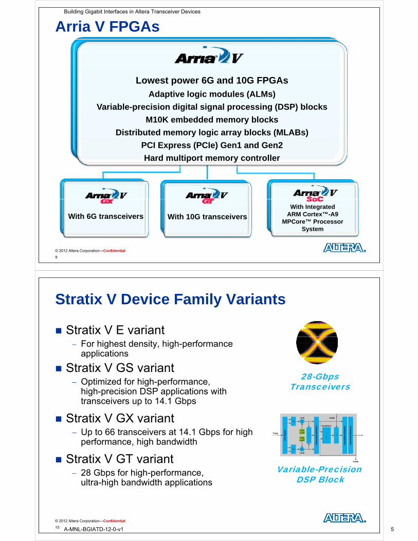
Arria V FPGAs
Lowest power 6G and 10G FPGAs
Adaptive logic modules (ALMs)
Variable-precision digital signal processing (DSP) blocks
M10K embedded memory blocks
Distributed memory logic array blocks (MLABs)Distributed memory logic array blocks (MLABs)
PCI Express (PCIe) Gen1 and Gen2
Hard multiport memory controller
With 6G transceivers With 10G transceiversWith Integrated
ARM Cortex™-A9 MPCore™ Processor
System
© 2012 Altera Corporation—Confidential
System
9
Stratix V Device Family Variants
Stratix V E variantF hi h t d it hi h f For highest density, high-performance applications
Stratix V GS variant28 Gb
Optimized for high-performance, high-precision DSP applications with transceivers up to 14.1 Gbps
28-GbpsTransceivers
p p
Stratix V GX variant Up to 66 transceivers at 14.1 Gbps for high
performance, high bandwidth
Stratix V GT variant 28 Gb f hi h f Variable Precision 28 Gbps for high-performance, ultra-high bandwidth applications
Variable-PrecisionDSP Block
© 2012 Altera Corporation—Confidential
10
Building Gigabit Interfaces in Altera Transceiver Devices
A-MNL-BGIATD-12-0-v1 5
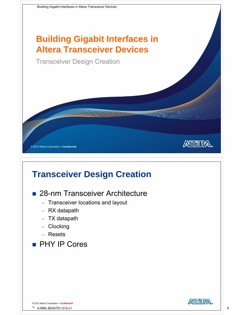
Building Gigabit Interfaces inBuilding Gigabit Interfaces in Altera Transceiver DevicesT i D i C tiTransceiver Design Creation
© 2012 Altera Corporation—Confidential
Transceiver Design Creation
28-nm Transceiver Architecture Transceiver locations and layout
RX datapath
TX datapath TX datapath
Clocking
ResetsResets
PHY IP Cores
© 2012 Altera Corporation—Confidential
12
Building Gigabit Interfaces in Altera Transceiver Devices
A-MNL-BGIATD-12-0-v1 6
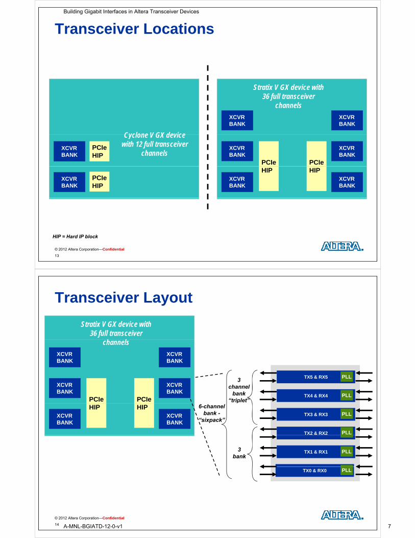
Transceiver Locations
Stratix V GX device with 36 full transceiver
h lchannels
XCVR BANK
XCVR BANK
Cyclone V GX device
XCVR BANK
XCVR BANK
Cyclone V GX device with 12 full transceiver
channelsXCVR BANK
PCIe
PCIeHIP
PCIe
XCVR BANK
XCVR BANK
XCVR BANK
HIPPCIeHIP
HIP
© 2012 Altera Corporation—Confidential
13
HIP = Hard IP block
Transceiver Layout
Stratix V GX device with 36 full transceiver
h lchannels
XCVR BANK
XCVR BANK
XCVR BANK
XCVR BANK
PCIePCIeTX4 & RX4
TX5 & RX53
channel bank
“triplet”
PLL
PLL
XCVR BANK
XCVR BANK
HIPHIPTX3 & RX3
TX2 & RX2
p6-channel
bank -“sixpack”
PLL
PLL
TX1 & RX13 bank
PLL
TX0 & RX0 PLL
© 2012 Altera Corporation—Confidential
14
Building Gigabit Interfaces in Altera Transceiver Devices
A-MNL-BGIATD-12-0-v1 7
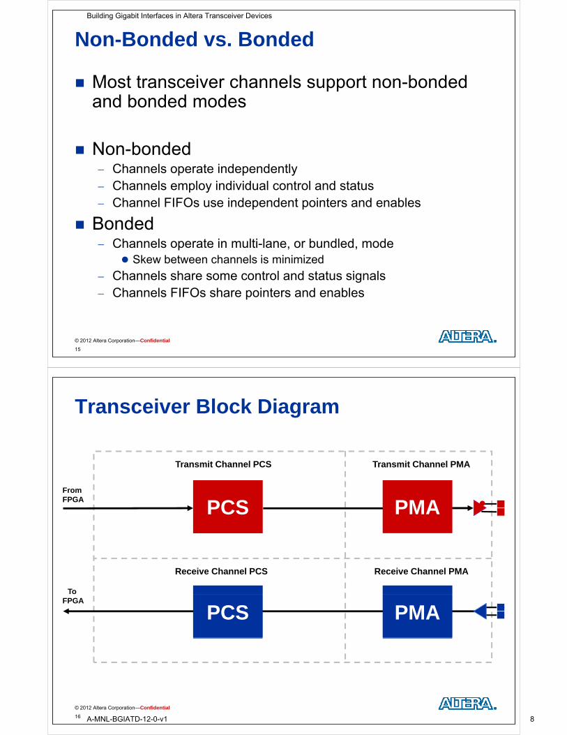
Non-Bonded vs. Bonded
Most transceiver channels support non-bonded d b d d dand bonded modes
Non-bonded Channels operate independently
Channels employ individual control and status Channels employ individual control and status Channel FIFOs use independent pointers and enables
Bonded Bonded Channels operate in multi-lane, or bundled, mode
Skew between channels is minimized
Channels share some control and status signals Channels FIFOs share pointers and enables
© 2012 Altera Corporation—Confidential
15
Transceiver Block Diagram
Transmit Channel PCS Transmit Channel PMA
FromFPGA
PCSPCS PMAPMA
Transmit Channel PCS Transmit Channel PMA
PCSPCS PMAPMA
To
Receive Channel PCS Receive Channel PMA
FPGA
PCSPCS PMAPMA
© 2012 Altera Corporation—Confidential
16
Building Gigabit Interfaces in Altera Transceiver Devices
A-MNL-BGIATD-12-0-v1 8
Transceiver Design Creation
28-nm Transceiver Architecture Transceiver locations and layout
RX datapath
TX datapath TX datapath
Clocking
ResetsResets
PHY IP Cores
© 2012 Altera Corporation—Confidential
17
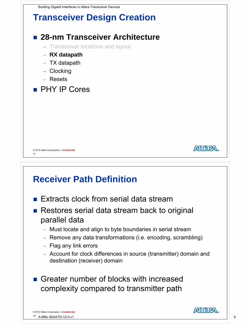
Receiver Path Definition
Extracts clock from serial data stream
Restores serial data stream back to original parallel data p Must locate and align to byte boundaries in serial stream
Remove any data transformations (i.e. encoding, scrambling)
Flag any link errors
Account for clock differences in source (transmitter) domain and destination (receiver) domaindestination (receiver) domain
Greater number of blocks with increased Greater number of blocks with increased complexity compared to transmitter path
© 2012 Altera Corporation—Confidential
18
Building Gigabit Interfaces in Altera Transceiver Devices
A-MNL-BGIATD-12-0-v1 9
Receiver Block Diagram
Receive Channel PCS Receive Channel PMA
To FPGA
Receive Channel PCS Receive Channel PMA
PCSPCS PMAPMAPCSPCS PMAPMA
© 2012 Altera Corporation—Confidential
19
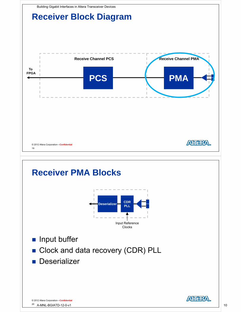
Receiver PMA Blocks
DeserializerCDRPLL
Input Reference Clocks
Input buffer
Clock and data recovery (CDR) PLL Clock and data recovery (CDR) PLL
Deserializer
© 2012 Altera Corporation—Confidential
20
Building Gigabit Interfaces in Altera Transceiver Devices
A-MNL-BGIATD-12-0-v1 10
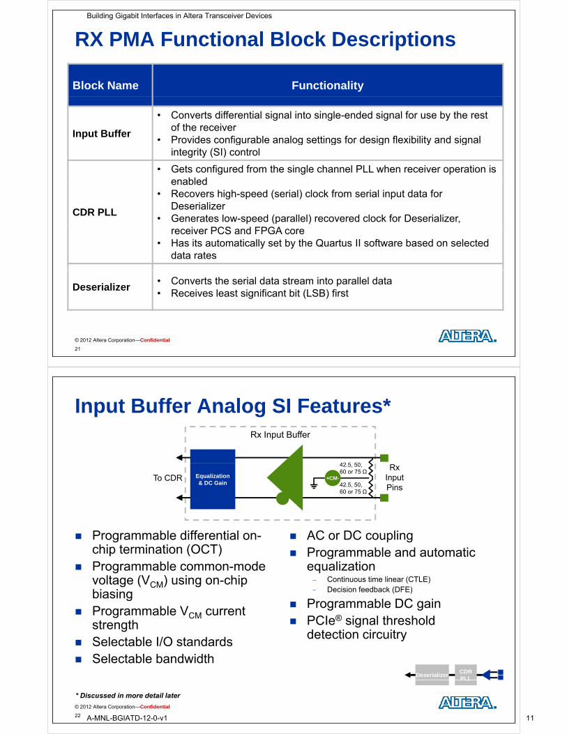
RX PMA Functional Block Descriptions
Block Name Functionality
Input Buffer
• Converts differential signal into single-ended signal for use by the rest of the receiver
• Provides configurable analog settings for design flexibility and signal• Provides configurable analog settings for design flexibility and signal integrity (SI) control
• Gets configured from the single channel PLL when receiver operation is enabled
CDR PLL
enabled• Recovers high-speed (serial) clock from serial input data for
Deserializer• Generates low-speed (parallel) recovered clock for Deserializer,
CS Greceiver PCS and FPGA core• Has its automatically set by the Quartus II software based on selected
data rates
Deserializer• Converts the serial data stream into parallel data• Receives least significant bit (LSB) first
© 2012 Altera Corporation—Confidential
21
Input Buffer Analog SI Features*Rx Input Buffer
42 5 50 Rx Input Pins
To CDR +CM-Equalization & DC Gain
42.5, 50,60 or 75 Ω
42.5, 50,60 or 75 Ω
Programmable differential on-chip termination (OCT)
AC or DC couplingProgrammable and automaticchip termination (OCT)
Programmable common-mode voltage (VCM) using on-chip biasing
Programmable and automatic equalization Continuous time linear (CTLE) Decision feedback (DFE)biasing
Programmable VCM current strengthS /O
( )
Programmable DC gain PCIe® signal threshold
detection circuitry Selectable I/O standards Selectable bandwidth
detection circuitry
DeserializerCDRPLL
© 2012 Altera Corporation—Confidential
22
PLL
* Discussed in more detail later
Building Gigabit Interfaces in Altera Transceiver Devices
A-MNL-BGIATD-12-0-v1 11
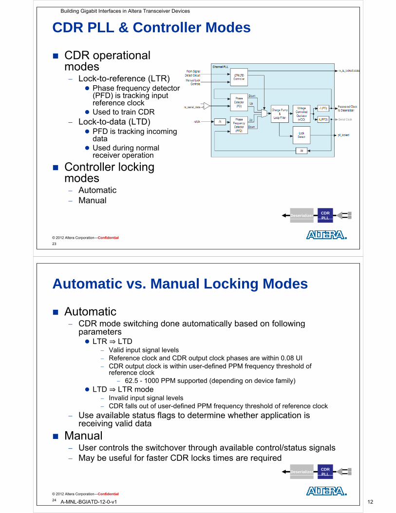
CDR PLL & Controller Modes
CDR operational modesmodes Lock-to-reference (LTR)
Phase frequency detector (PFD) is tracking input(PFD) is tracking input reference clock
Used to train CDR Lock-to-data (LTD)
PFD is tracking incoming data
Used during normal receiver operationp
Controller locking modes
Automatic Automatic Manual
DeserializerCDRPLL
© 2012 Altera Corporation—Confidential
23
PLL
Automatic vs. Manual Locking Modes
AutomaticCDR mode switching done automatically based on following CDR mode switching done automatically based on following parameters LTR ⇒ LTD
Valid input signal levels Reference clock and CDR output clock phases are within 0.08 UI CDR output clock is within user-defined PPM frequency threshold of
reference clock 62.5 - 1000 PPM supported (depending on device family)
LTD ⇒ LTR mode Invalid input signal levels CDR falls out of user-defined PPM frequency threshold of reference clock
Use available status flags to determine whether application is Use available status flags to determine whether application is receiving valid data
ManualU t l th it h th h il bl t l/ t t i l User controls the switchover through available control/status signals
May be useful for faster CDR locks times are required
DeserializerCDRPLL
© 2012 Altera Corporation—Confidential
24
PLL
Building Gigabit Interfaces in Altera Transceiver Devices
A-MNL-BGIATD-12-0-v1 12
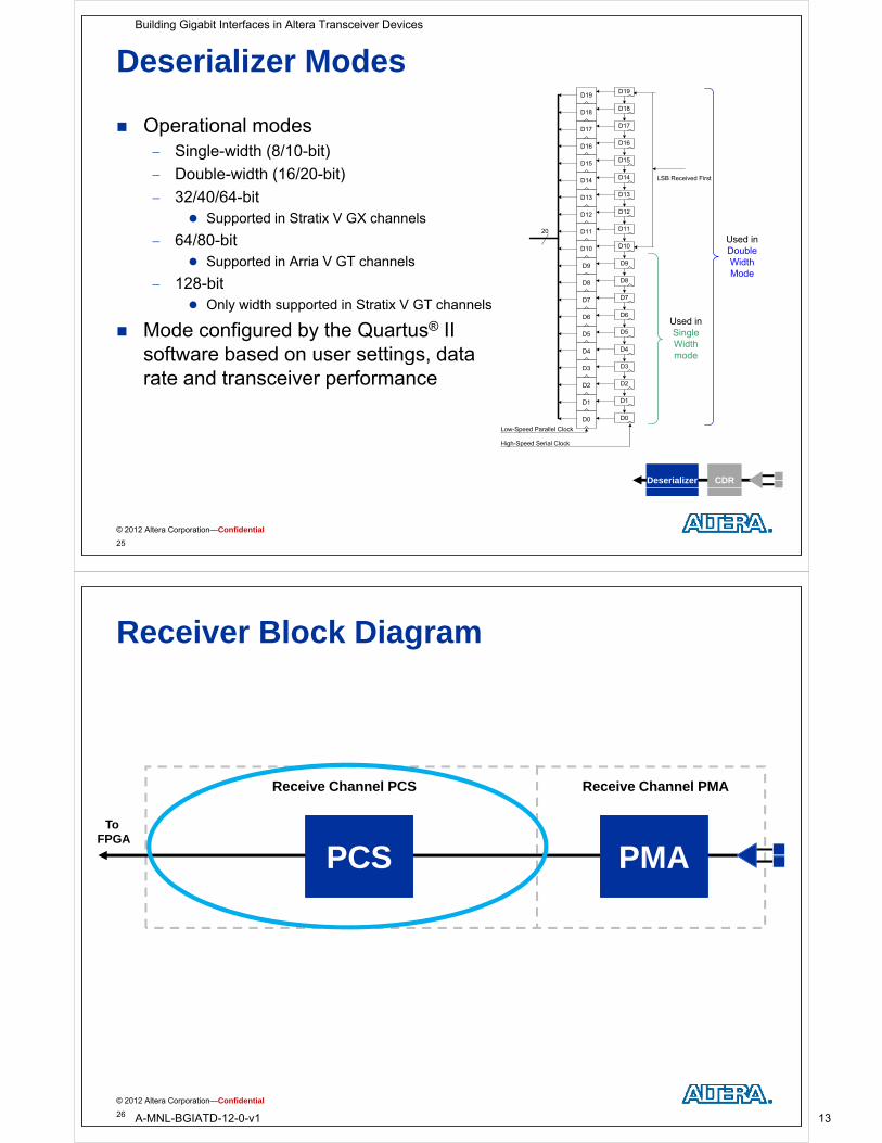
Deserializer Modes
Operational modesSingle width (8/10 bit)
D18
D19
D16
D17
D19
D18
D17
D16
Single-width (8/10-bit)
Double-width (16/20-bit)
32/40/64-bit Supported in Stratix V GX channels
D14
D15
D12
D13
D15
D14
D13
D12
LSB Received First
Supported in Stratix V GX channels
64/80-bit Supported in Arria V GT channels
128-bit
D10
D11
D8
D9
D11
D10
D9
D8
Used inDouble Width Mode
20
128 bit Only width supported in Stratix V GT channels
Mode configured by the Quartus® II software based on user settings data
D6
D7
D4
D5
D7
D6
D5
D4
Used inSingle Width
dsoftware based on user settings, data rate and transceiver performance
D4
D2
D3
D0
D1
D3
D2
D1
D0
mode
D0
Low-Speed Parallel Clock
High-Speed Serial Clock
Deserializer CDR
© 2012 Altera Corporation—Confidential
25
Receiver Block Diagram
Receive Channel PCS Receive Channel PMA
To FPGA
Receive Channel PCS Receive Channel PMA
PCSPCS PMAPMAPCSPCS PMAPMA
© 2012 Altera Corporation—Confidential
26
Building Gigabit Interfaces in Altera Transceiver Devices
A-MNL-BGIATD-12-0-v1 13
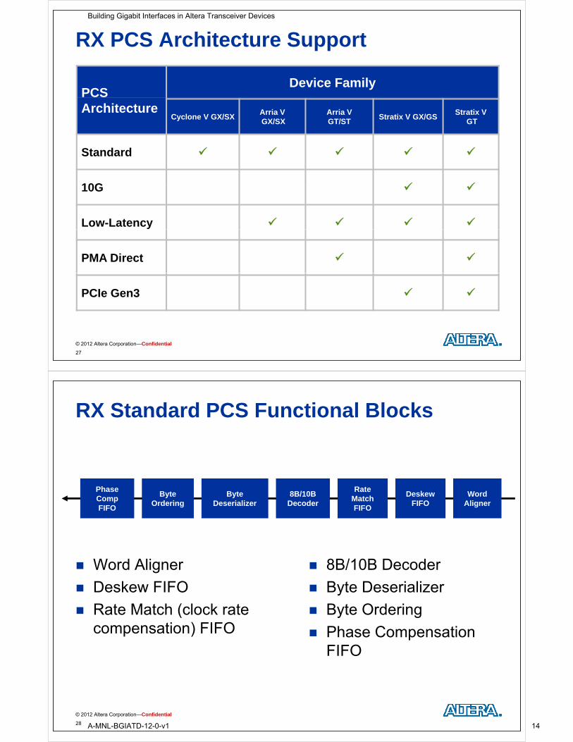
RX PCS Architecture Support
PCSDevice Family
ArchitectureCyclone V GX/SX
Arria VGX/SX
Arria V GT/ST
Stratix V GX/GSStratix V
GT
Standard
10G 10G
Low-Latency
PMA Direct
PCIe Gen3
© 2012 Altera Corporation—Confidential
27
RX Standard PCS Functional Blocks
PhaseCompFIFO
Byte Ordering
Byte Deserializer
8B/10B Decoder
RateMatchFIFO
WordAligner
DeskewFIFO
Word Aligner
Deskew FIFO
8B/10B Decoder
Byte Deserializer
Rate Match (clock rate compensation) FIFO
Byte Ordering
Phase Compensation FIFO
© 2012 Altera Corporation—Confidential
28
Building Gigabit Interfaces in Altera Transceiver Devices
A-MNL-BGIATD-12-0-v1 14
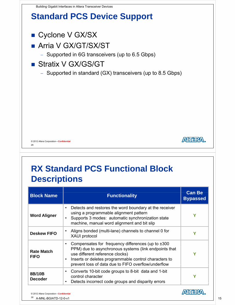
Standard PCS Device Support
Cyclone V GX/SX
Arria V GX/GT/SX/ST Supported in 6G transceivers (up to 6.5 Gbps)
Stratix V GX/GS/GT Supported in standard (GX) transceivers (up to 8.5 Gbps)
© 2012 Altera Corporation—Confidential
29
RX Standard PCS Functional Block Descriptions
Can BeBlock Name Functionality
Can BeBypassed
• Detects and restores the word boundary at the receiver
Word Alignerusing a programmable alignment pattern
• Supports 3 modes: automatic synchronization state machine, manual word alignment and bit slip
Y
Deskew FIFO• Aligns bonded (multi-lane) channels to channel 0 for
XAUI protocolY
• Compensates for frequency differences (up to ±300
Rate Match FIFO
PPM) due to asynchronous systems (link endpoints that use different reference clocks)
• Inserts or deletes programmable control characters to prevent loss of data due to FIFO overflow/underflow
Y
prevent loss of data due to FIFO overflow/underflow
8B/10BDecoder
• Converts 10-bit code groups to 8-bit data and 1-bit control character
• Detects incorrect code groups and disparity errorsY
© 2012 Altera Corporation—Confidential
30
Detects incorrect code groups and disparity errors
Building Gigabit Interfaces in Altera Transceiver Devices
A-MNL-BGIATD-12-0-v1 15
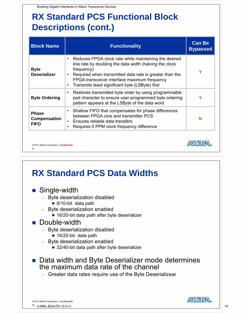
RX Standard PCS Functional Block Descriptions (cont.)
C BBlock Name Functionality
Can BeBypassed
• Reduces FPGA clock rate while maintaining the desired
ByteDeserializer
Reduces FPGA clock rate while maintaining the desired line rate by doubling the data width (halving the clockfrequency)
• Required when transmitted data rate is greater than the FPGA t i i t f i f
Y
FPGA-transceiver interface maximum frequency• Transmits least significant byte (LSByte) first
B t O d i• Restores transmitted byte order by using programmable
d h t t d b t d i YByte Ordering pad character to ensure user-programmed byte ordering pattern appears at the LSByte of the data word
Y
Phase• Shallow FIFO that compensates for phase differences
between FPGA core and transmitter PCSCompensation FIFO
between FPGA core and transmitter PCS• Ensures reliable data transfers• Requires 0 PPM clock frequency difference
N
© 2012 Altera Corporation—Confidential
31
RX Standard PCS Data Widths
Single-widthByte deserialization disabled Byte deserialization disabled 8/10-bit data path
Byte deserialization enabled 16/20-bit data path after byte deserializer 16/20 bit data path after byte deserializer
Double-width Byte deserialization disabled
16/20 bit d t th 16/20-bit data path Byte deserialization enabled
32/40-bit data path after byte deserializer
Data width and Byte Deserializer mode determines the maximum data rate of the channel Greater data rates require use of the Byte Deserializear
© 2012 Altera Corporation—Confidential
32
Building Gigabit Interfaces in Altera Transceiver Devices
A-MNL-BGIATD-12-0-v1 16
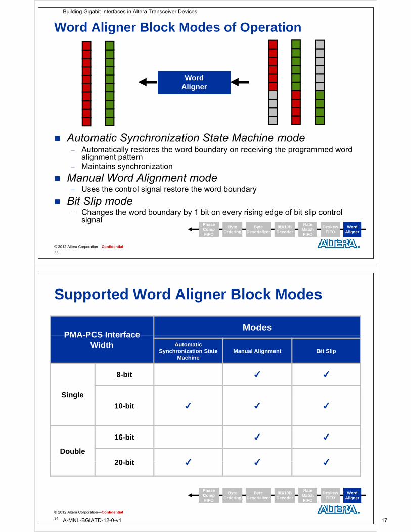
Word Aligner Block Modes of Operation
WordAligner
Automatic Synchronization State Machine mode Automatically restores the word boundary on receiving the programmed word
alignment patternM i t i h i ti Maintains synchronization
Manual Word Alignment mode Uses the control signal restore the word boundary
Bit Slip mode Changes the word boundary by 1 bit on every rising edge of bit slip control
signalPhase
Byte Byte 8B/10BRate
WordDeskew
© 2012 Altera Corporation—Confidential
33
CompFIFO
Byte Ordering
Byte Deserializer
8B/10B Decoder
Match FIFO
Word Aligner
DeskewFIFO
Supported Word Aligner Block Modes
PMA-PCS InterfaceModes
PMA-PCS Interface Width Automatic
Synchronization State Machine
Manual Alignment Bit Slip
Single
8-bit
g
10-bit
Double
16-bit
20 bit 20-bit
PhaseByte Byte 8B/10B
Rate WordDeskew
© 2012 Altera Corporation—Confidential
34
CompFIFO
Byte Ordering
Byte Deserializer
8B/10B Decoder
Match FIFO
Word Aligner
DeskewFIFO
Building Gigabit Interfaces in Altera Transceiver Devices
A-MNL-BGIATD-12-0-v1 17
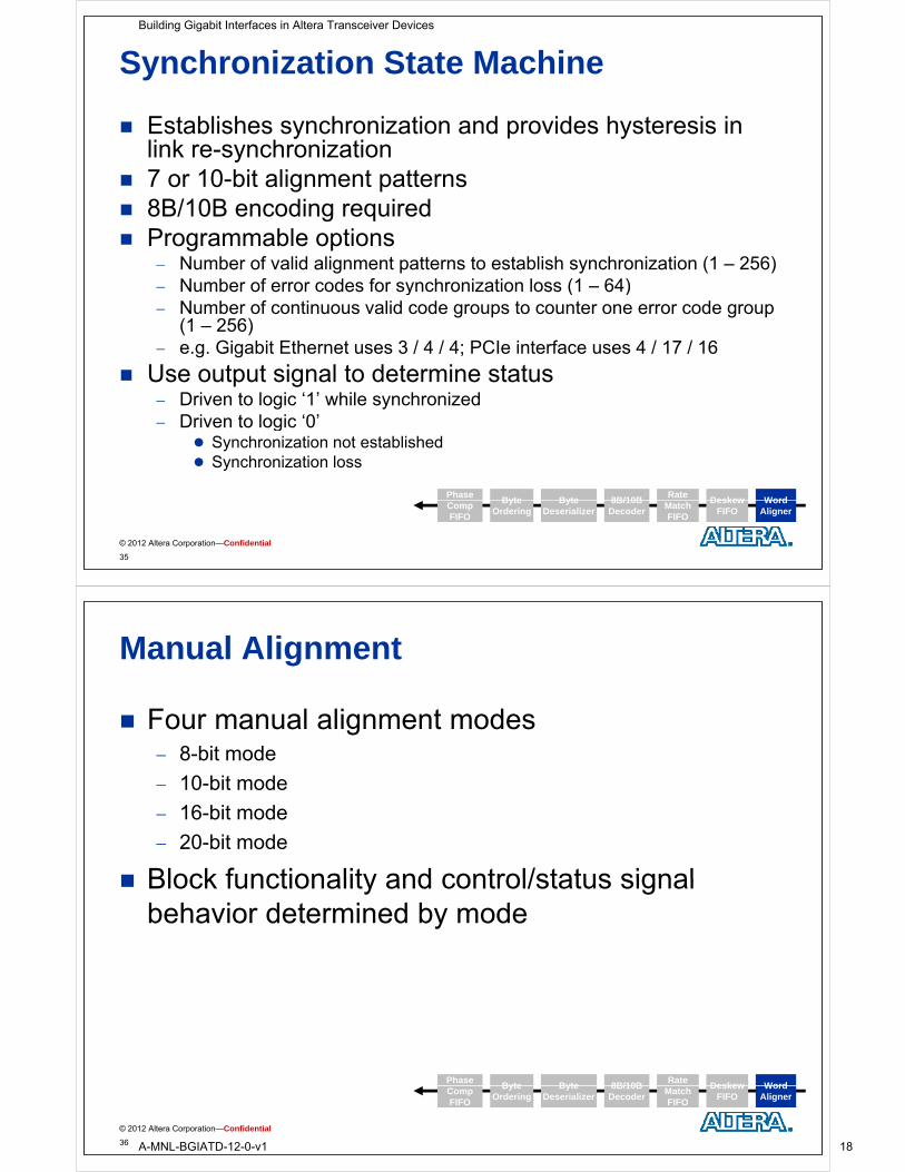
Synchronization State Machine
Establishes synchronization and provides hysteresis in link re-synchronizationlink re synchronization
7 or 10-bit alignment patterns 8B/10B encoding required Programmable options
Number of valid alignment patterns to establish synchronization (1 – 256) Number of error codes for synchronization loss (1 – 64)y ( ) Number of continuous valid code groups to counter one error code group
(1 – 256) e.g. Gigabit Ethernet uses 3 / 4 / 4; PCIe interface uses 4 / 17 / 16
Use output signal to determine status Driven to logic ‘1’ while synchronized Driven to logic ‘0’ g
Synchronization not established Synchronization loss
PhaseByte Byte 8B/10B
Rate WordDeskew
© 2012 Altera Corporation—Confidential
35
CompFIFO
Byte Ordering
Byte Deserializer
8B/10B Decoder
Match FIFO
Word Aligner
DeskewFIFO
Manual Alignment
Four manual alignment modes 8-bit mode
10-bit mode
16 bit mode 16-bit mode
20-bit mode
Block functionality and control/status signal Block functionality and control/status signal behavior determined by mode
PhaseByte Byte 8B/10B
Rate WordDeskew
© 2012 Altera Corporation—Confidential
36
CompFIFO
Byte Ordering
Byte Deserializer
8B/10B Decoder
Match FIFO
Word Aligner
DeskewFIFO
Building Gigabit Interfaces in Altera Transceiver Devices
A-MNL-BGIATD-12-0-v1 18
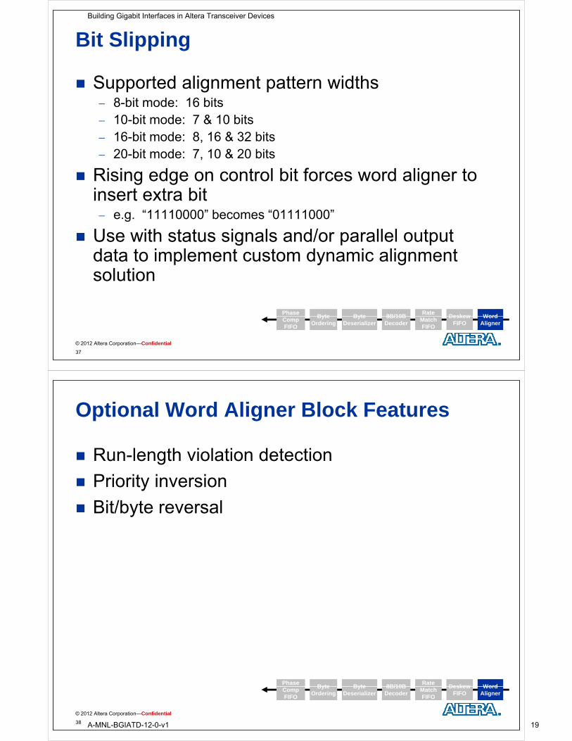
Bit Slipping
Supported alignment pattern widths8 bi d 16 bi 8-bit mode: 16 bits
10-bit mode: 7 & 10 bits 16-bit mode: 8, 16 & 32 bits, 20-bit mode: 7, 10 & 20 bits
Rising edge on control bit forces word aligner to insert extra bit e.g. “11110000” becomes “01111000”
U i h i l d/ ll l Use with status signals and/or parallel output data to implement custom dynamic alignment solutionsolution
PhaseByte Byte 8B/10B
Rate WordDeskew
© 2012 Altera Corporation—Confidential
37
CompFIFO
Byte Ordering
Byte Deserializer
8B/10B Decoder
Match FIFO
Word Aligner
DeskewFIFO
Optional Word Aligner Block Features
Run-length violation detection
Priority inversion
Bit/byte reversal Bit/byte reversal
PhaseByte Byte 8B/10B
Rate WordDeskew
© 2012 Altera Corporation—Confidential
38
CompFIFO
Byte Ordering
Byte Deserializer
8B/10B Decoder
Match FIFO
Word Aligner
DeskewFIFO
Building Gigabit Interfaces in Altera Transceiver Devices
A-MNL-BGIATD-12-0-v1 19

Run Length Violation Detection
Detector flags programmable threshold of ti 1’ d 0’ i th i d d tconsecutive 1’s and 0’s in the received data
Output signal asserted when run length violation d t t ddetected
PhaseByte Byte 8B/10B
Rate WordDeskew
© 2012 Altera Corporation—Confidential
39
CompFIFO
Byte Ordering
Byte Deserializer
8B/10B Decoder
Match FIFO
Word Aligner
DeskewFIFO
Receiver Polarity Inversion
Correct situations where positive and negative legs of the diff ti l li k l d d i b ddifferential link are erroneously swapped during board layout
Dynamically controlled Dynamically controlled Logic ‘1’ inverts the polarity of every bit received at the input of the word
aligner1
0
0
0
1
1
Bit 7
0
1
1
0
1
0
0
1
10001100
0
0
1
1 Bit 0
PhaseByte Byte 8B/10B
Rate WordDeskew
© 2012 Altera Corporation—Confidential
40
CompFIFO
Byte Ordering
Byte Deserializer
8B/10B Decoder
Match FIFO
Word Aligner
DeskewFIFO
Building Gigabit Interfaces in Altera Transceiver Devices
A-MNL-BGIATD-12-0-v1 20
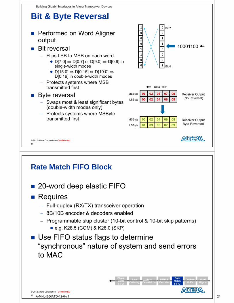
Bit & Byte Reversal
Performed on Word Aligner output
1
0
0
0
0
1
Bit 7
output Bit reversal
Flips LSB to MSB on each word
0
1
1
1
0
0
10001100
p D[7:0] D[0:7] or D[9:0] D[0:9] in
single-width modes D[15:0] D[0:15] or D[19:0]
D[0:19] in double width modes
0
0
0
1 Bit 0
D[0:19] in double-width modes
Protects systems where MSB transmitted first
B t l 01 03 05 07 09
Data Flow
MSByte R i O t t Byte reversal Swaps most & least significant bytes
(double-width modes only)
01 03 05 07 09
00 02 04 06 08
MSByte
LSByte
Receiver Output (No Reversal)
Protects systems where MSBytetransmitted first 00 02 04 06 08
01 03 05 07 09
MSByte
LSByte
Receiver Output Byte-Reversed
© 2012 Altera Corporation—Confidential
41
Rate Match FIFO Block
20-word deep elastic FIFO
Requires Full-duplex (RX/TX) transceiver operation
8B/10B encoder & decoders enabled
Programmable skip cluster (10-bit control & 10-bit skip patterns) e g K28 5 (COM) & K28 0 (SKP) e.g. K28.5 (COM) & K28.0 (SKP)
Use FIFO status flags to determine “synchronous” nature of system and send errorssynchronous nature of system and send errors to MAC
PhaseComp
Byte Byte 8B/10B Rate
MatchWord Deskew
© 2012 Altera Corporation—Confidential
42
CompFIFO
yOrdering
yDeserializer Decoder
MatchFIFIO
AlignerFIFO
Building Gigabit Interfaces in Altera Transceiver Devices
A-MNL-BGIATD-12-0-v1 21
Rate Matching Insertion & Deletion
Single-width Insertion: Up to four skip patterns such that there are no more
than five skip patterns in the skip cluster after insertion
Deletion: Up to four skip patterns such that there is at least one Deletion: Up to four skip patterns such that there is at least oneskip pattern left in the SKIP cluster after deletion
Double-widthDouble width Insertion: As many pairs of skip patterns in a skip cluster as
necessary
Deletion: As many pairs of skip patterns from a skip cluster as necessary Skip patterns must appear both LSByte and MSByte of same 20-bit p p pp y y
word
© 2012 Altera Corporation—Confidential
43
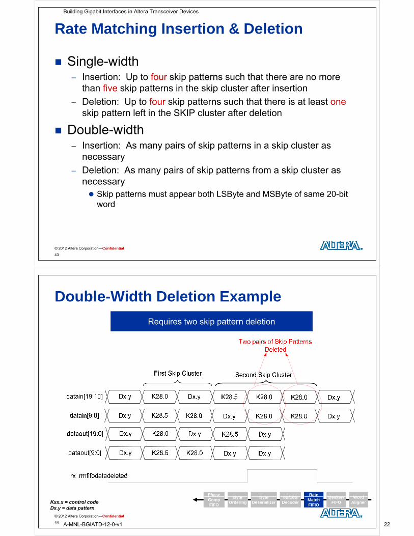
Double-Width Deletion Example
Requires two skip pattern deletion
PhaseByte Byte 8B/10B
Rate WordDeskew
© 2012 Altera Corporation—Confidential
44
CompFIFO
Byte Ordering
Byte Deserializer
8B/10B Decoder
MatchFIFIO
Word Aligner
DeskewFIFOKxx.x = control code
Dx.y = data pattern
Building Gigabit Interfaces in Altera Transceiver Devices
A-MNL-BGIATD-12-0-v1 22
Rate Matching Full & Empty
Single-width Full: Data word that filled the FIFO is deleted
Empty: K30.7 character inserted after last word is removed
Double-widthF ll P i f d th t fill d th FIFO d l t d Full: Pair of words that filled the FIFO are deleted
Empty: Pair of K30.7 characters are inserted after last word is removed
PhaseComp
Byte Byte 8B/10B Rate
MatchWord Deskew
© 2012 Altera Corporation—Confidential
45
CompFIFO
yOrdering
yDeserializer Decoder
MatchFIFIO
AlignerFIFO
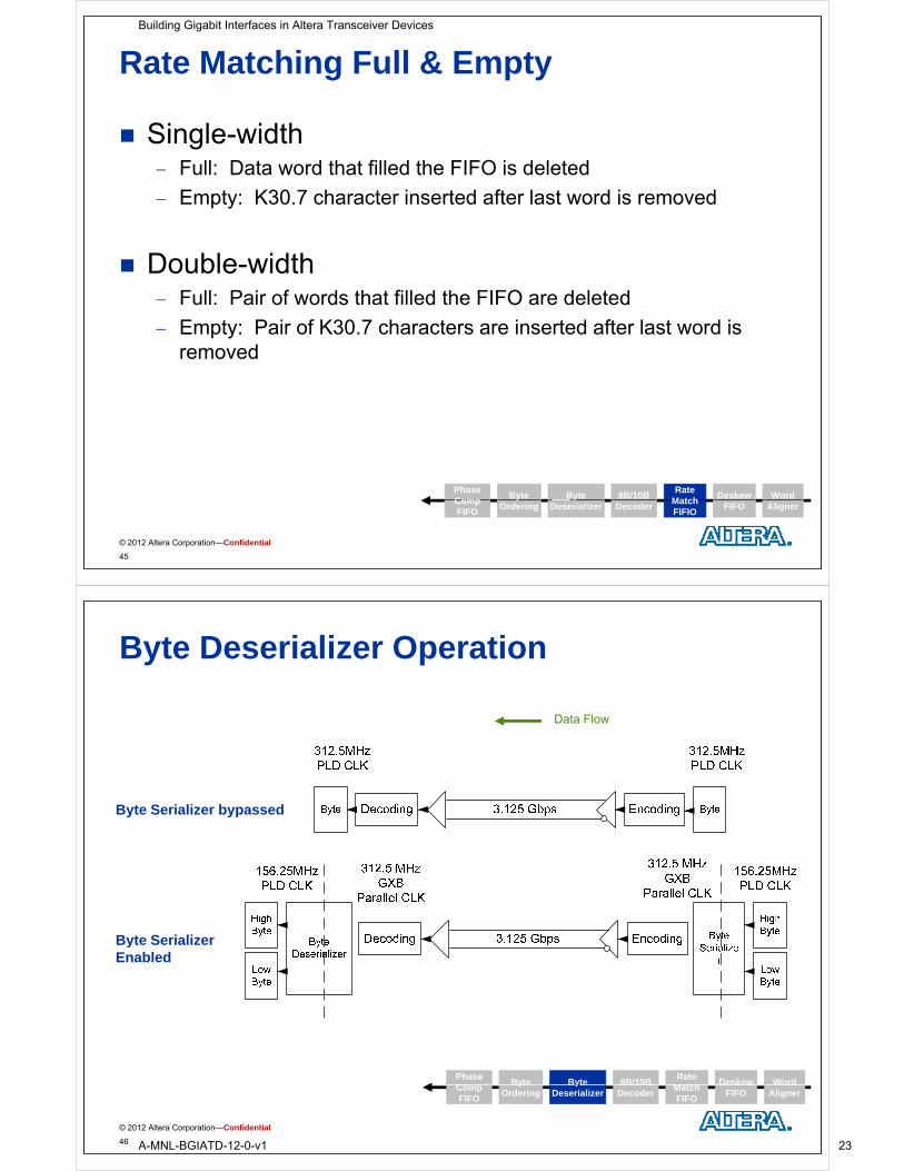
Byte Deserializer Operation
Data Flow
Byte Serializer bypassedByte Serializer bypassed
Byte Serializer yEnabled
PhaseC
Byte Byte 8B/10BRate
M t hWordDeskew
© 2012 Altera Corporation—Confidential
46
CompFIFO
Byte Ordering
Byte Deserializer
8B/10B Decoder
Match FIFO
Word Aligner
DeskewFIFO
Building Gigabit Interfaces in Altera Transceiver Devices
A-MNL-BGIATD-12-0-v1 23

Byte Ordering Block
Requires Requires Pre-defined byte-ordering pattern (bit width based upon transceiver
configuration)
Pre-defined pad character (bit width based upon transceiver configuration)
Can be user-controlled or Word Aligner controlled Can be user-controlled or Word Aligner controlled
PhaseComp
Byte Byte 8B/10B Rate
MatchWord Deskew
© 2012 Altera Corporation—Confidential
47
CompFIFO
yOrdering
yDeserializer Decoder
Match FIFO
AlignerFIFO
RX 10G PCS Blocks
Receiver Gearbox Bit Error Rate (BER) Block Synchronizer
Disparity Checker
Monitor
64B/66B Decoderspa ty C ec e
Descrambler
Frame Synchronizer
CRC-32 Checker
Receiver FIFO Frame Synchronizer Receiver FIFO
RX FIFO
CRC-32 Checker
De-Scrambler
Frame Synch
64B/66B Decoder
Disparity Checker
Receiver Gearbox
Block Synch
BER Monitor
© 2012 Altera Corporation—Confidential
48
Building Gigabit Interfaces in Altera Transceiver Devices
A-MNL-BGIATD-12-0-v1 24
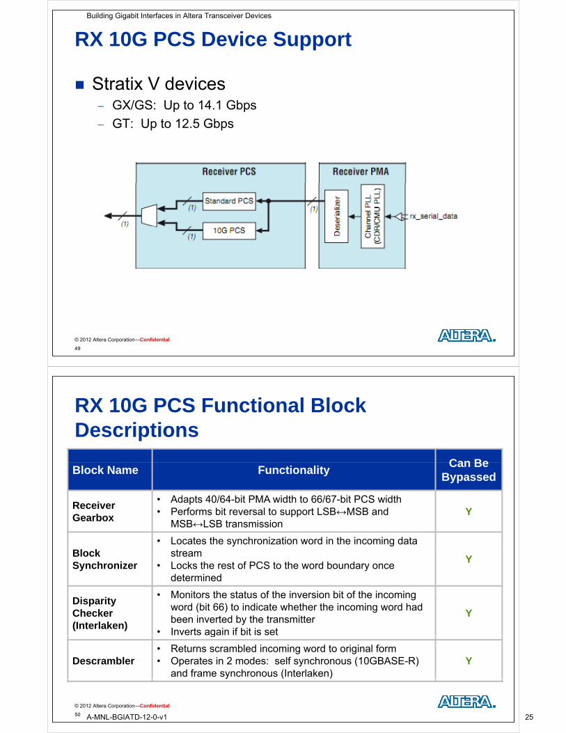
RX 10G PCS Device Support
Stratix V devices GX/GS: Up to 14.1 Gbps
GT: Up to 12.5 Gbps
© 2012 Altera Corporation—Confidential
49
RX 10G PCS Functional Block Descriptions
Can BeBlock Name Functionality
Can BeBypassed
Receiver• Adapts 40/64-bit PMA width to 66/67-bit PCS width
Receiver Gearbox
• Performs bit reversal to support LSB↔MSB and MSB↔LSB transmission
Y
Bl k• Locates the synchronization word in the incoming data
Block Synchronizer
stream• Locks the rest of PCS to the word boundary once
determined
Y
M it th t t f th i i bit f th i iDisparity Checker(Interlaken)
• Monitors the status of the inversion bit of the incoming word (bit 66) to indicate whether the incoming word had been inverted by the transmitter
• Inverts again if bit is set
Y
g
Descrambler• Returns scrambled incoming word to original form • Operates in 2 modes: self synchronous (10GBASE-R)
and frame synchronous (Interlaken)Y
© 2012 Altera Corporation—Confidential
50
Building Gigabit Interfaces in Altera Transceiver Devices
A-MNL-BGIATD-12-0-v1 25
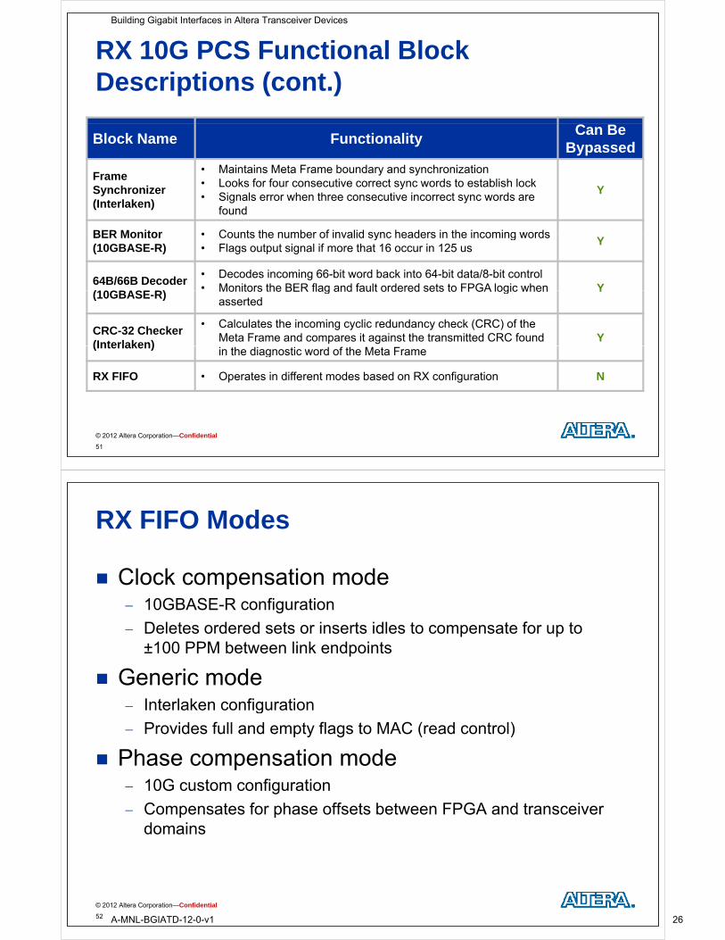
RX 10G PCS Functional Block Descriptions (cont.)
Block Name FunctionalityCan Be
Bypassed
Frame• Maintains Meta Frame boundary and synchronization
L k f f ti t d t t bli h l kFrameSynchronizer (Interlaken)
• Looks for four consecutive correct sync words to establish lock• Signals error when three consecutive incorrect sync words are
found
Y
BER Monitor • Counts the number of invalid sync headers in the incoming wordsBER Monitor(10GBASE-R)
• Counts the number of invalid sync headers in the incoming words• Flags output signal if more that 16 occur in 125 us
Y
64B/66B Decoder(10GBASE R)
• Decodes incoming 66-bit word back into 64-bit data/8-bit control• Monitors the BER flag and fault ordered sets to FPGA logic when Y
(10GBASE-R)Monitors the BER flag and fault ordered sets to FPGA logic when asserted
Y
CRC-32 Checker (Interlaken)
• Calculates the incoming cyclic redundancy check (CRC) of the Meta Frame and compares it against the transmitted CRC found Y
(Interlaken)in the diagnostic word of the Meta Frame
RX FIFO • Operates in different modes based on RX configuration N
© 2012 Altera Corporation—Confidential
51
RX FIFO Modes
Clock compensation mode 10GBASE-R configuration
Deletes ordered sets or inserts idles to compensate for up to ±100 PPM between link endpoints±100 PPM between link endpoints
Generic modeInterlaken configuration Interlaken configuration
Provides full and empty flags to MAC (read control)
Phase compensation mode Phase compensation mode 10G custom configuration
Compensates for phase offsets between FPGA and transceiver p pdomains
© 2012 Altera Corporation—Confidential
52
Building Gigabit Interfaces in Altera Transceiver Devices
A-MNL-BGIATD-12-0-v1 26
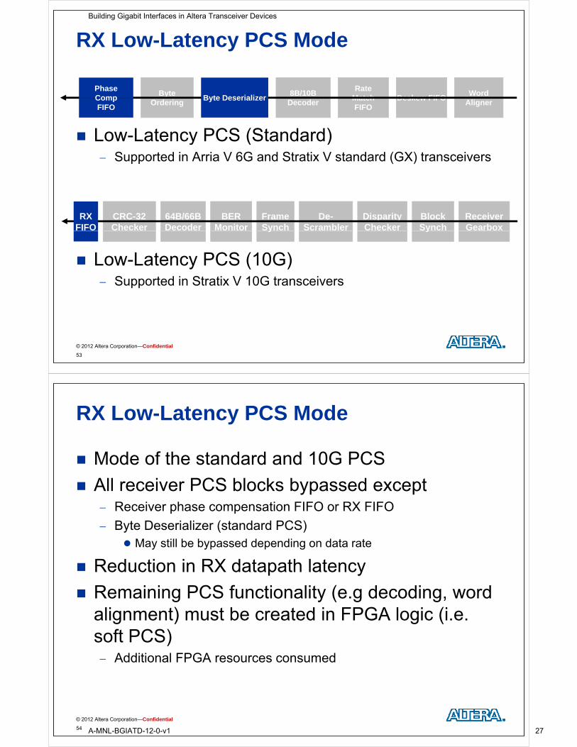
RX Low-Latency PCS Mode
Byte 8B/10B Rate
MatchWord
Deskew FIFOPhaseComp Byte Deserializer
Low-Latency PCS (Standard)
Ordering DecoderMatchFIFO
AlignerDeskew FIFOComp
FIFOByte Deserializer
y ( ) Supported in Arria V 6G and Stratix V standard (GX) transceivers
CRC-32 Checker
De-Scrambler
Frame Synch
64B/66B Decoder
Disparity Checker
Receiver Gearbox
Block Synch
BER Monitor
RX FIFO
Low-Latency PCS (10G)
y y
Supported in Stratix V 10G transceivers
© 2012 Altera Corporation—Confidential
53
RX Low-Latency PCS Mode
Mode of the standard and 10G PCS
All receiver PCS blocks bypassed except Receiver phase compensation FIFO or RX FIFO
Byte Deserializer (standard PCS) May still be bypassed depending on data rate
R d ti i RX d t th l t Reduction in RX datapath latency
Remaining PCS functionality (e.g decoding, word alignment) must be created in FPGA logic (i.e. soft PCS) Additional FPGA resources consumed
© 2012 Altera Corporation—Confidential
54
Building Gigabit Interfaces in Altera Transceiver Devices
A-MNL-BGIATD-12-0-v1 27
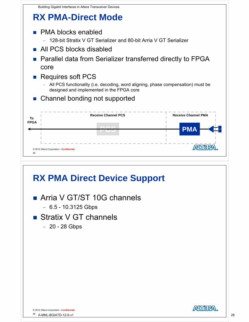
RX PMA-Direct Mode
PMA blocks enabled 128-bit Stratix V GT Serializer and 80-bit Arria V GT Serializer
All PCS blocks disabled
Parallel data from Serializer transferred directly to FPGA ycore
Requires soft PCS All PCS functionality (i.e. decoding, word aligning, phase compensation) must be
designed and implemented in the FPGA core
Channel bonding not supported Channel bonding not supported
ToReceive Channel PCS Receive Channel PMA
PCSPCS
To FPGA
PMAPMA
© 2012 Altera Corporation—Confidential
55
RX PMA Direct Device Support
Arria V GT/ST 10G channels 6.5 - 10.3125 Gbps
Stratix V GT channels 20 - 28 Gbps
© 2012 Altera Corporation—Confidential
56
Building Gigabit Interfaces in Altera Transceiver Devices
A-MNL-BGIATD-12-0-v1 28
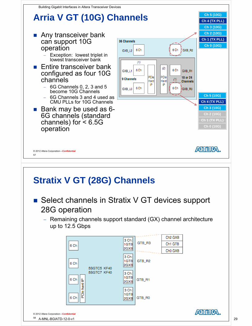
Arria V GT (10G) Channels Ch 5 (10G)
Ch 4 (TX PLL)
Any transceiver bank can support 10G
Ch 3 (10G)
Ch 2 (10G)
Ch 1 (TX PLL)can support 10G operation Exception: lowest triplet in
lowest transceiver bank
Ch 0 (10G)
Entire transceiver bank configured as four 10G channelschannels 6G Channels 0, 2, 3 and 5
become 10G Channels 6G Channels 3 and 4 used as
CMU PLL f 10G Ch l
Ch 5 (10G)
Ch 4 (TX PLL)CMU PLLs for 10G Channels
Bank may be used as 6-6G channels (standard h l ) f 6 5G
Ch 4 (TX PLL)
Ch 3 (10G)
Ch 2 (10G)
Ch 1 (TX PLL)channels) for < 6.5G operation
Ch 1 (TX PLL)
Ch 0 (10G)
© 2012 Altera Corporation—Confidential
57
Stratix V GT (28G) Channels
Select channels in Stratix V GT devices support 28G operation Remaining channels support standard (GX) channel architecture
up to 12 5 Gbpsup to 12.5 Gbps
© 2012 Altera Corporation—Confidential
58
Building Gigabit Interfaces in Altera Transceiver Devices
A-MNL-BGIATD-12-0-v1 29
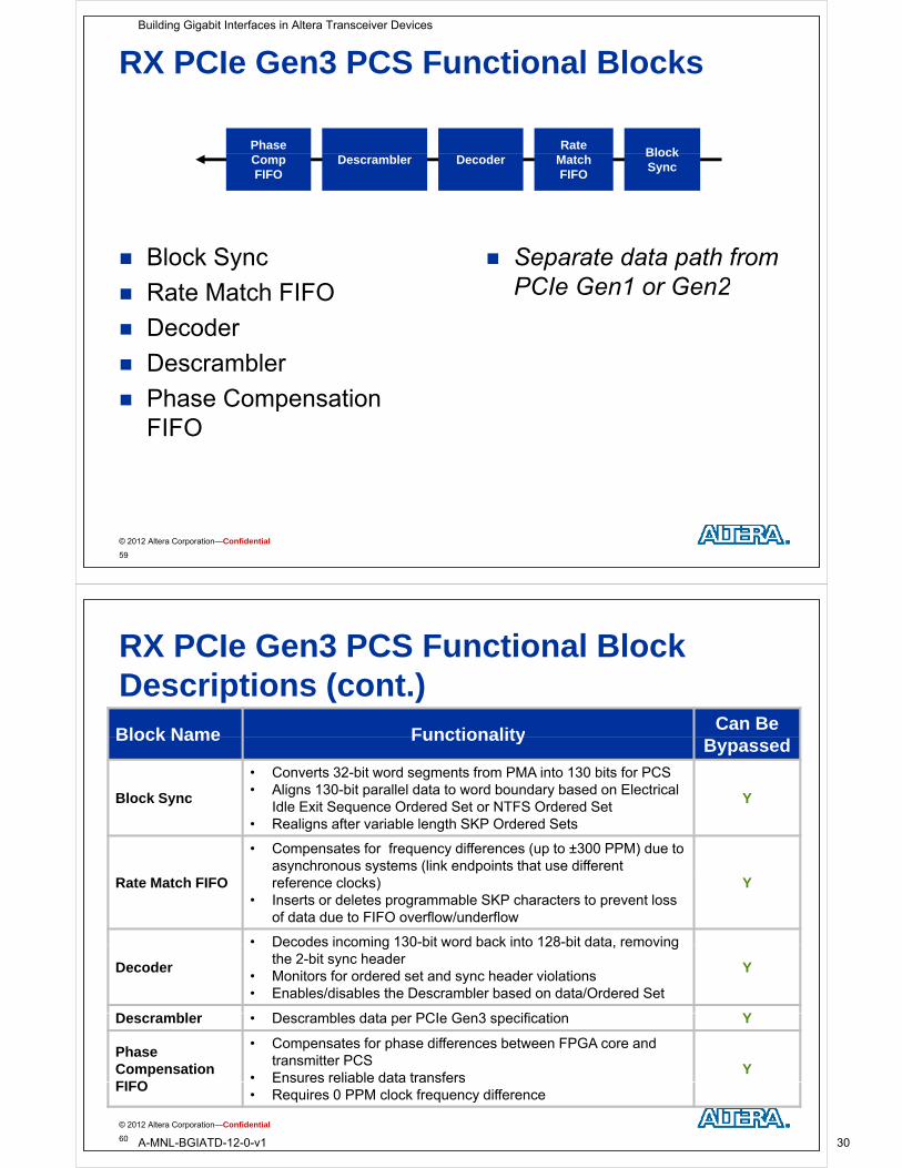
RX PCIe Gen3 PCS Functional Blocks
PhaseBlock
RateCompFIFO
Descrambler DecoderBlockSync
MatchFIFO
Block Sync
Rate Match FIFO
Separate data path from PCIe Gen1 or Gen2 Rate Match FIFO
Decoder
Descrambler
PCIe Gen1 or Gen2
Descrambler
Phase Compensation FIFOFIFO
© 2012 Altera Corporation—Confidential
59
RX PCIe Gen3 PCS Functional Block Descriptions (cont.)Block Name Functionality
Can BeBlock Name Functionality
Bypassed
Block Sync
• Converts 32-bit word segments from PMA into 130 bits for PCS• Aligns 130-bit parallel data to word boundary based on Electrical
Idle Exit Sequence Ordered Set or NTFS Ordered SetY
Idle Exit Sequence Ordered Set or NTFS Ordered Set• Realigns after variable length SKP Ordered Sets
• Compensates for frequency differences (up to ±300 PPM) due to asynchronous systems (link endpoints that use different
Rate Match FIFO reference clocks)• Inserts or deletes programmable SKP characters to prevent loss
of data due to FIFO overflow/underflow
Y
• Decodes incoming 130-bit word back into 128-bit data removing
Decoder
Decodes incoming 130 bit word back into 128 bit data, removing the 2-bit sync header
• Monitors for ordered set and sync header violations• Enables/disables the Descrambler based on data/Ordered Set
Y
D bl D bl d t PCI G 3 ifi ti YDescrambler • Descrambles data per PCIe Gen3 specification Y
PhaseCompensation FIFO
• Compensates for phase differences between FPGA core and transmitter PCS
• Ensures reliable data transfersY
© 2012 Altera Corporation—Confidential
60
FIFOEnsures reliable data transfers
• Requires 0 PPM clock frequency difference
Building Gigabit Interfaces in Altera Transceiver Devices
A-MNL-BGIATD-12-0-v1 30

Transceiver Design Creation
28-nm Transceiver Architecture Transceiver locations and layout
RX datapath
TX datapath TX datapath
Clocking
ResetsResets
PHY IP Cores
© 2012 Altera Corporation—Confidential
61
Transmitter Path Definition
Converts parallel data pattern to high-speed serial data stream
Embeds clock into single serial data stream so gdata can be restored at receiver
Functionally simpler & fewer blocks when compared to receivercompared to receiver
© 2012 Altera Corporation—Confidential
62
Building Gigabit Interfaces in Altera Transceiver Devices
A-MNL-BGIATD-12-0-v1 31
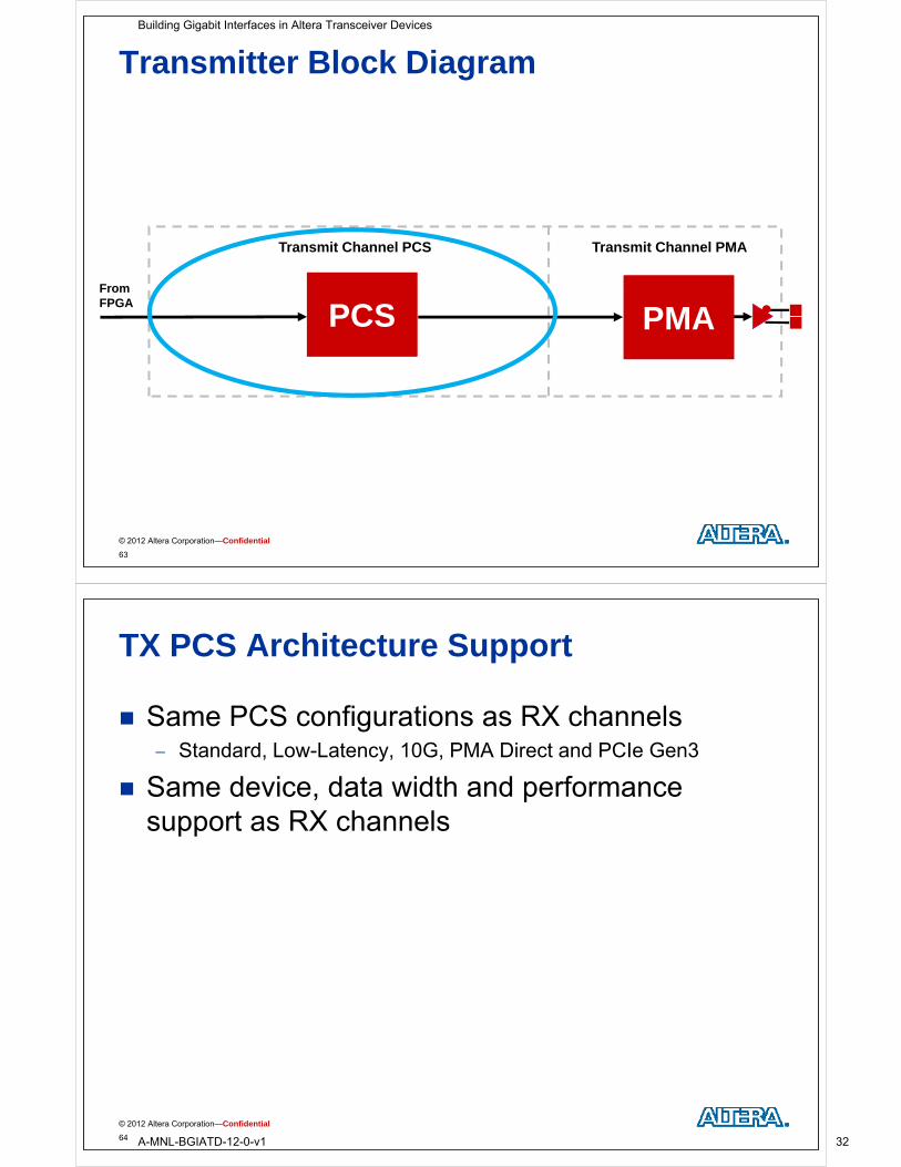
Transmitter Block Diagram
From
Transmit Channel PCS Transmit Channel PMA
FromFPGA
PCSPCS PMAPMA
© 2012 Altera Corporation—Confidential
63
TX PCS Architecture Support
Same PCS configurations as RX channels Standard, Low-Latency, 10G, PMA Direct and PCIe Gen3
Same device, data width and performance support as RX channels
© 2012 Altera Corporation—Confidential
64
Building Gigabit Interfaces in Altera Transceiver Devices
A-MNL-BGIATD-12-0-v1 32
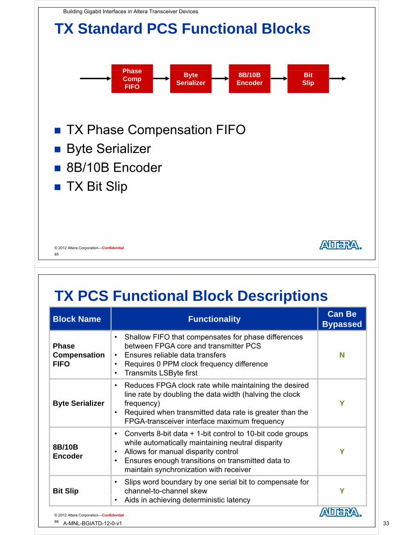
TX Standard PCS Functional Blocks
PhasePhase Comp FIFO
Byte Serializer
8B/10B Encoder
BitSlip
TX Phase Compensation FIFOTX Phase Compensation FIFO
Byte Serializer
8B/10B Encoder 8B/10B Encoder
TX Bit Slip
© 2012 Altera Corporation—Confidential
65
TX PCS Functional Block Descriptions
Block Name FunctionalityCan Be
Bypassed
• Shallow FIFO that compensates for phase differencesPhase CompensationFIFO
• Shallow FIFO that compensates for phase differences between FPGA core and transmitter PCS
• Ensures reliable data transfers• Requires 0 PPM clock frequency difference
N
• Transmits LSByte first
B t S i li
• Reduces FPGA clock rate while maintaining the desired line rate by doubling the data width (halving the clockf ) YByte Serializer frequency)
• Required when transmitted data rate is greater than the FPGA-transceiver interface maximum frequency
Y
Converts 8 bit data + 1 bit control to 10 bit code groups
8B/10B Encoder
• Converts 8-bit data + 1-bit control to 10-bit code groups while automatically maintaining neutral disparity
• Allows for manual disparity control• Ensures enough transitions on transmitted data to
Yg
maintain synchronization with receiver
Bit Slip• Slips word boundary by one serial bit to compensate for
channel-to-channel skew Y
© 2012 Altera Corporation—Confidential
66
• Aids in achieving deterministic latency
Building Gigabit Interfaces in Altera Transceiver Devices
A-MNL-BGIATD-12-0-v1 33
TX 10G Functional PCS Blocks
Transmitter FIFO Scrambler
Frame Generator
CRC-32 Generator
Disparity Generator
Transmitter Gearbox CRC 32 Generator
64B/66B Encoder
Transmitter Gearbox
TX FIFO
CRC-32 Generator
ScramblerFrame
Generator64B/66B Encoder
Disparity Generator
Transmitter Gearbox
© 2012 Altera Corporation—Confidential
67
TX 10G PCS Functional Block Descriptions
Block Name FunctionalityCan Be
Block Name FunctionalityBypassed
TX FIFO • Provides timing interface between FPGA and PCS N
Frame Generator
• Forms the Meta Frame from transmitted data and control words
• Encapsulates payload with Meta Frame control words YGenerator (Interlaken)
Encapsulates payload with Meta Frame control words (synchronization, scrambler state, skip control and diagnostic)
Y
CRC-32 Calculates CRC value of the Meta Frame (excluding a
Generator (Interlaken)
• Calculates CRC value of the Meta Frame (excluding a few bits) and embeds into diagnostic word
Y
64B/66B • Encodes 64-bit data/8-bit control from transmitter FIFO Encoder(10GBASE-R)
into 66-bit word• Controls DC balancing and disparity
Y
© 2012 Altera Corporation—Confidential
68
Building Gigabit Interfaces in Altera Transceiver Devices
A-MNL-BGIATD-12-0-v1 34
TX 10G PCS Functional Block Descriptions (cont.)
Can BeBlock Name Functionality
Can BeBypassed
• Reduces EMI effects by applying polynomial to data,
Scrambler
removing long sequences of 0’s/1’s and repetitious patterns
• Further ensures ample transitions so clock can be extracted from data
Yextracted from data
• Operates in 2 modes: self synchronous (10GBASE-R) and frame synchronous (Interlaken)
Di it• Maintains DC balance by monitoring disparity and
Disparity Generator(Interlaken)
Maintains DC balance by monitoring disparity and inverting words as needed to maintain neutral disparity
• Sets bit 66 to indicate to receiver that current word has been inverted
Y
Transmitter Gearbox
• Adapts 66/67-bit PCS output to 40/64-bit input to the PMA to support the target line rate
• Reverses word to support LSB↔MSB and MSB↔LSB transmission
Y
© 2012 Altera Corporation—Confidential
69
transmission
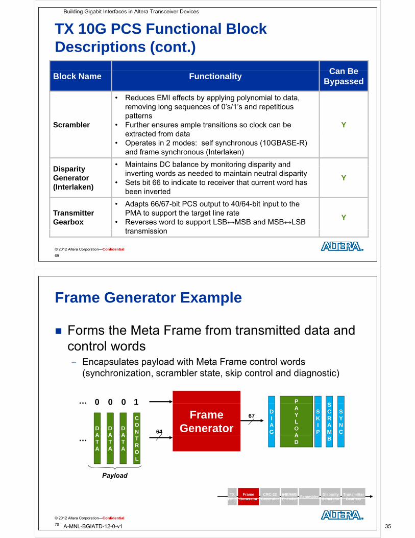
Frame Generator Example
Forms the Meta Frame from transmitted data and control words Encapsulates payload with Meta Frame control words
(synchronization scrambler state skip control and diagnostic)(synchronization, scrambler state, skip control and diagnostic)
P1000… S
Frame Generator64
PAYLOA
DA
DA
DA
1000…
CON
SYNC
67
SCRAM
SKIP
DIAG
AD
ATA
ATA
ATA
… TROL
B
TX FIFO
CRC-32 Generator
ScramblerFrame
Generator64B/66B Encoder
Disparity Generator
Transmitter Gearbox
Payload
© 2012 Altera Corporation—Confidential
70
FIFO GeneratorGenerator Encoder Generator Gearbox
Building Gigabit Interfaces in Altera Transceiver Devices
A-MNL-BGIATD-12-0-v1 35
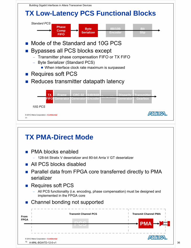
TX Low-Latency PCS Functional Blocks
Phase Comp
Byte Serializer
8B/10B Encoder
BitSlip
Standard PCS
Mode of the Standard and 10G PCS
FIFOSerializer Encoder Slip
Bypasses all PCS blocks except Transmitter phase compensation FIFO or TX FIFO
Byte Serializer (Standard PCS) Byte Serializer (Standard PCS) When interface clock rate maximum is surpassed
Requires soft PCSq Reduces transmitter datapath latency
CRC-32 Generator
ScramblerFrame
Generator64B/66B Encoder
Disparity Generator
Transmitter Gearbox
TX FIFO
10G PCS
© 2012 Altera Corporation—Confidential
71
10G PCS
TX PMA-Direct Mode
PMA blocks enabled128 bit St ti V d i li d 80 bit A i V GT d i li 128-bit Stratix V deserializer and 80-bit Arria V GT deserializer
All PCS blocks disabled
Parallel data from FPGA core transferred directly to PMA Parallel data from FPGA core transferred directly to PMA serializer
Requires soft PCS Requires soft PCS All PCS functionality (i.e. encoding, phase compensation) must be designed and
implemented in the FPGA core
Ch l b di t t d Channel bonding not supported
Transmit Channel PCS Transmit Channel PMA
PCSPCSFromFPGA
PMAPMA
© 2012 Altera Corporation—Confidential
72
Building Gigabit Interfaces in Altera Transceiver Devices
A-MNL-BGIATD-12-0-v1 36
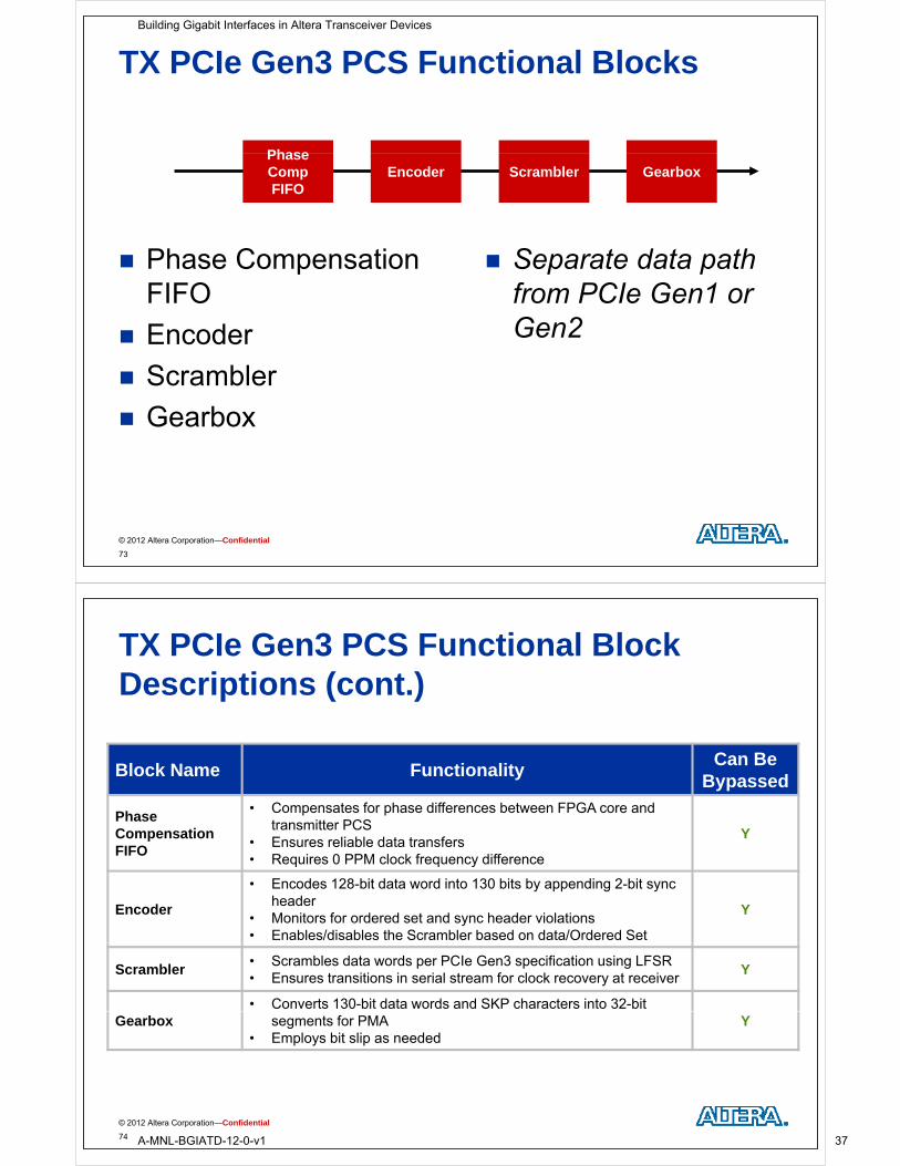
TX PCIe Gen3 PCS Functional Blocks
PhasePhase Comp FIFO
Encoder Scrambler Gearbox
Phase Compensation FIFO
Separate data path from PCIe Gen1 orFIFO
Encoder
from PCIe Gen1 or Gen2
Scrambler
Gearbox
© 2012 Altera Corporation—Confidential
73
TX PCIe Gen3 PCS Functional Block Descriptions (cont.)
Block Name FunctionalityCan Be
BypassedC t f h diff b t FPGA d
PhaseCompensation FIFO
• Compensates for phase differences between FPGA core and transmitter PCS
• Ensures reliable data transfers• Requires 0 PPM clock frequency difference
Y
Encoder
• Encodes 128-bit data word into 130 bits by appending 2-bit sync header
• Monitors for ordered set and sync header violations• Enables/disables the Scrambler based on data/Ordered Set
Y
Scrambler• Scrambles data words per PCIe Gen3 specification using LFSR• Ensures transitions in serial stream for clock recovery at receiver
Y
• Converts 130-bit data words and SKP characters into 32-bit Gearbox segments for PMA
• Employs bit slip as needed Y
© 2012 Altera Corporation—Confidential
74
Building Gigabit Interfaces in Altera Transceiver Devices
A-MNL-BGIATD-12-0-v1 37

Transmitter Block Diagram
From
Transmit Channel PCS Transmit Channel PMA
FromFPGA
PCSPCS PMAPMA
© 2012 Altera Corporation—Confidential
75
Transmitter PMA Functional Blocks
SerializerBit
Output BufferBit
Serializer
Block Name Functionality
Serializer
• Converts the parallel data into serial data stream• Transmits LSB first
Serializer• Supports same operational modes (widths) as Deserializer• Includes optional controls for polarity inversion and bit reversal
• Converts single-ended signal into differential signal for transmission
Output Bufferacross the serial link
• Provides configurable analog settings for design flexibility and signal integrity control
© 2012 Altera Corporation—Confidential
76
Building Gigabit Interfaces in Altera Transceiver Devices
A-MNL-BGIATD-12-0-v1 38
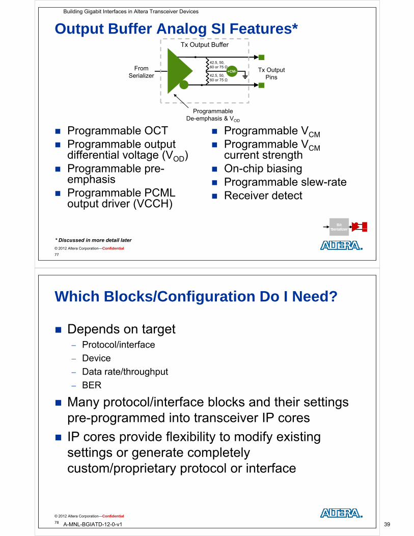
Output Buffer Analog SI Features*
42.5, 50,60 or 75 Ω
Tx Output+CM
Tx Output Buffer
From Tx Output Pins
+CM-Serializer 42.5, 50,
60 or 75 Ω
Programmable OCT Programmable VCM
Programmable De-emphasis & VOD
Programmable OCT Programmable output
differential voltage (VOD)P bl
Programmable VCM
Programmable VCMcurrent strengthO hi bi i Programmable pre-
emphasis Programmable PCML
On-chip biasing Programmable slew-rate Receiver detectg
output driver (VCCH) Receiver detect
Bit Serializer
© 2012 Altera Corporation—Confidential
77
Serializer
* Discussed in more detail later
Which Blocks/Configuration Do I Need?
Depends on target Protocol/interface
Device
Data rate/throughput Data rate/throughput
BER
Many protocol/interface blocks and their settings Many protocol/interface blocks and their settings pre-programmed into transceiver IP cores
IP id fl ibilit t dif i ti IP cores provide flexibility to modify existing settings or generate completely
t / i t t l i t fcustom/proprietary protocol or interface
© 2012 Altera Corporation—Confidential
78
Building Gigabit Interfaces in Altera Transceiver Devices
A-MNL-BGIATD-12-0-v1 39
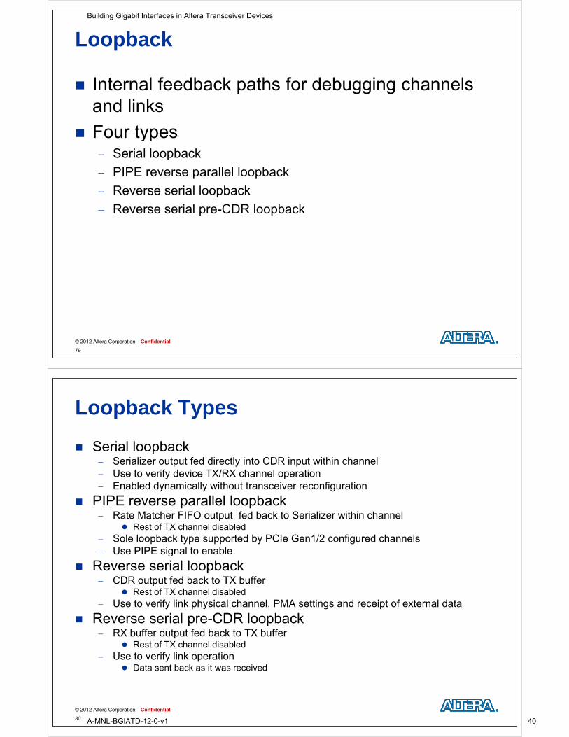
Loopback
Internal feedback paths for debugging channels and links
Four typesyp Serial loopback
PIPE reverse parallel loopback
Reverse serial loopback
Reverse serial pre-CDR loopback
© 2012 Altera Corporation—Confidential
79
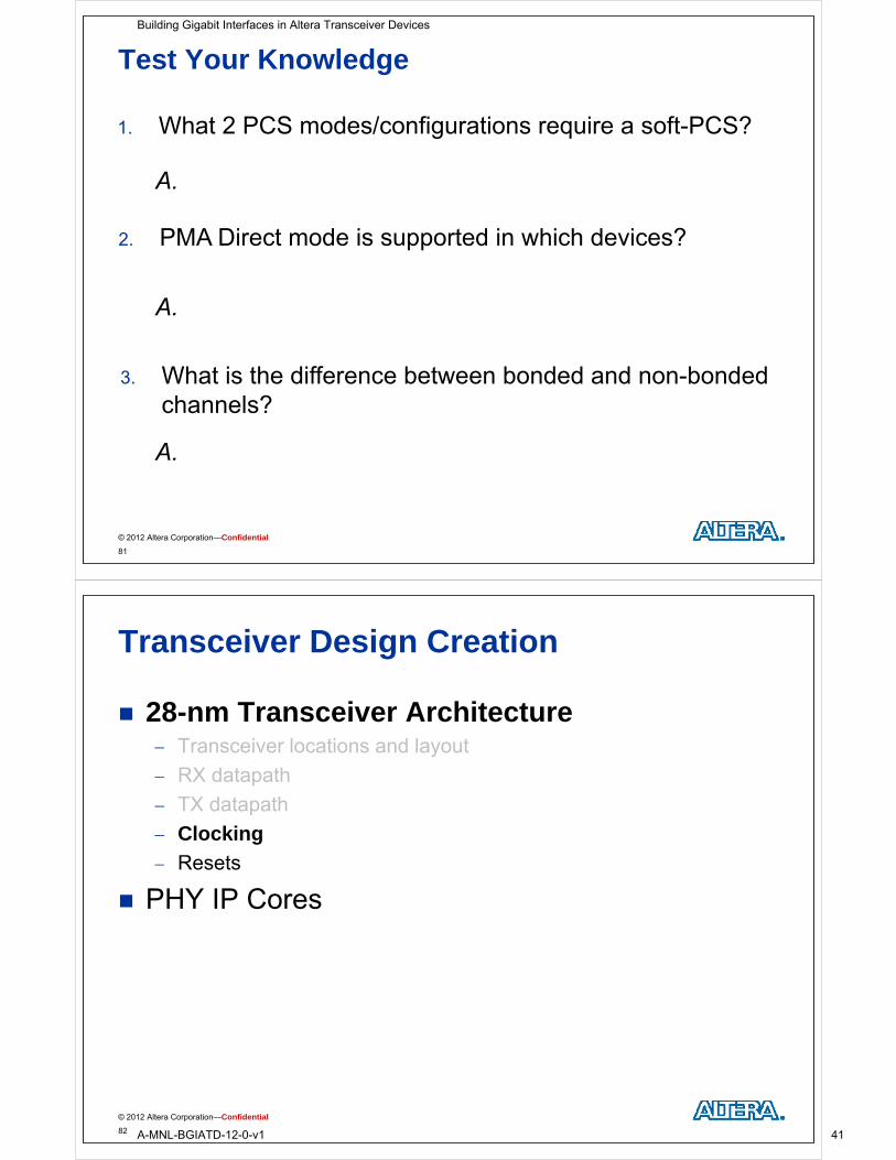
Loopback Types
Serial loopback Serializer output fed directly into CDR input within channelp y p Use to verify device TX/RX channel operation Enabled dynamically without transceiver reconfiguration
PIPE reverse parallel loopback Rate Matcher FIFO output fed back to Serializer within channel
Rest of TX channel disabled Sole loopback type supported by PCIe Gen1/2 configured channels Use PIPE signal to enableUse PIPE signal to enable
Reverse serial loopback CDR output fed back to TX buffer
Rest of TX channel disabled Use to verify link physical channel, PMA settings and receipt of external data
Reverse serial pre-CDR loopback RX buffer output fed back to TX buffer
Rest of TX channel disabled Use to verify link operation
Data sent back as it was received
© 2012 Altera Corporation—Confidential
80
Building Gigabit Interfaces in Altera Transceiver Devices
A-MNL-BGIATD-12-0-v1 40
Test Your Knowledge
1. What 2 PCS modes/configurations require a soft-PCS?
A. Low Latency and PMA Direct
2. PMA Direct mode is supported in which devices?
A. Arria V GT and Stratix V GT
3. What is the difference between bonded and non-bonded channels?
A. Non-bonded channels function independently, while bonded channels are linked.
© 2012 Altera Corporation—Confidential
81
Transceiver Design Creation
28-nm Transceiver Architecture Transceiver locations and layout
RX datapath
TX datapath TX datapath
Clocking
ResetsResets
PHY IP Cores
© 2012 Altera Corporation—Confidential
82
Building Gigabit Interfaces in Altera Transceiver Devices
A-MNL-BGIATD-12-0-v1 41
Transceiver Clocking
Transmit clock generation
Input reference clock sources
FPGA fabric clocks FPGA fabric clocks
© 2012 Altera Corporation—Confidential
83
Transmit Clock Generation*
TX or Clock Management Unit (CMU) PLLs
Auxiliary Transmit (ATX) PLLs
Fractional PLLs (fPLLs) Fractional PLLs (fPLLs)
TX Local Clock Dividers
TX C t l Cl k Di id TX Central Clock Dividers
© 2012 Altera Corporation—Confidential
84
* Each channel has a PLL that will be used as a CDR PLL when RX functionality is enabled.
Building Gigabit Interfaces in Altera Transceiver Devices
A-MNL-BGIATD-12-0-v1 42
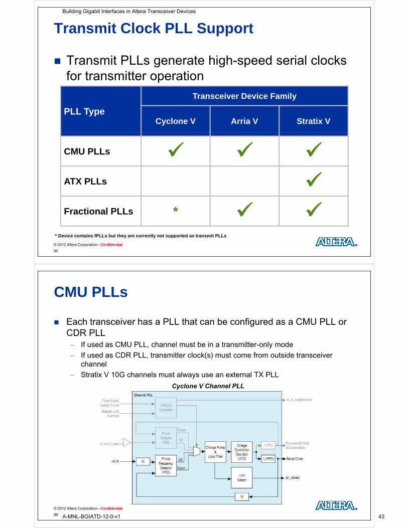
Transmit Clock PLL Support
Transmit PLLs generate high-speed serial clocks for transmitter operation
Transceiver Device Family
PLL TypeCyclone V Arria V Stratix V
CMU PLLs ATX PLLs Fractional PLLs *
© 2012 Altera Corporation—Confidential
85
* Device contains fPLLs but they are currently not supported as transmit PLLs
CMU PLLs
Each transceiver has a PLL that can be configured as a CMU PLL or CDR PLLCDR PLL If used as CMU PLL, channel must be in a transmitter-only mode
If used as CDR PLL, transmitter clock(s) must come from outside transceiver channelchannel
Stratix V 10G channels must always use an external TX PLL
Cyclone V Channel PLL
© 2012 Altera Corporation—Confidential
86
Building Gigabit Interfaces in Altera Transceiver Devices
A-MNL-BGIATD-12-0-v1 43
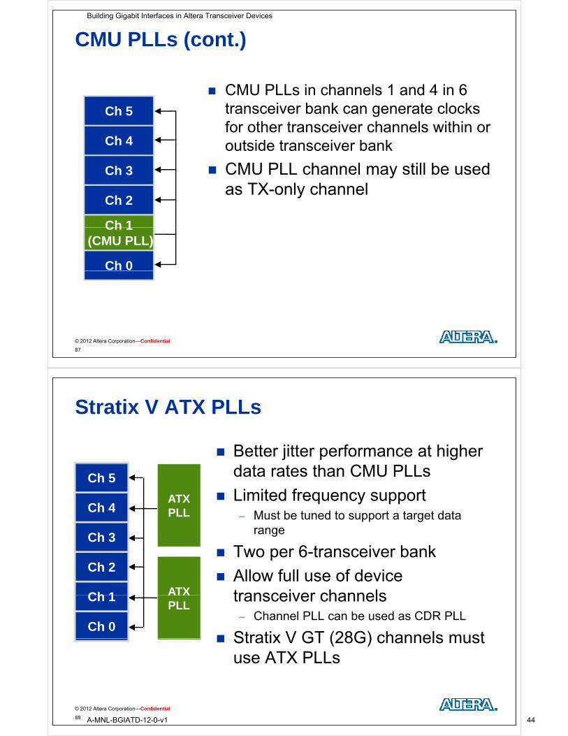
CMU PLLs (cont.)
CMU PLLs in channels 1 and 4 in 6 transceiver bank can generate clocks for other transceiver channels within or
t id t i b k
Ch 5
Ch 4 outside transceiver bank
CMU PLL channel may still be used TX l h l
Ch 4
Ch 3
as TX-only channelCh 2
Ch 1Ch 1(CMU PLL)
Ch 0
© 2012 Altera Corporation—Confidential
87
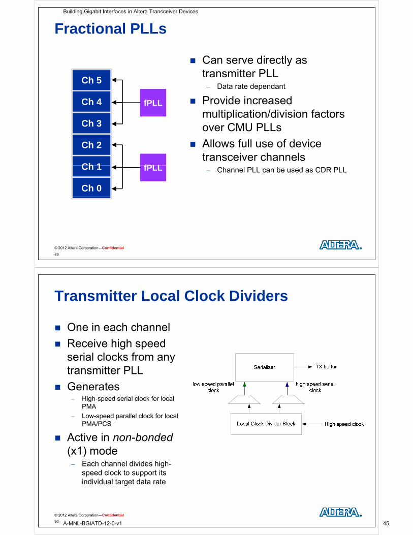
Stratix V ATX PLLs
Better jitter performance at higher d h CMU PLLdata rates than CMU PLLs
Limited frequency supportATX
Ch 5
Ch 4 Must be tuned to support a target data
range
Two per 6 transceiver bank
PLLCh 4
Ch 3 Two per 6-transceiver bank
Allow full use of device transceiver channelsATX
Ch 2
Ch 1 transceiver channels Channel PLL can be used as CDR PLL
Stratix V GT (28G) channels must
ATX PLL
Ch 1
Ch 0 Stratix V GT (28G) channels must
use ATX PLLs
© 2012 Altera Corporation—Confidential
88
Building Gigabit Interfaces in Altera Transceiver Devices
A-MNL-BGIATD-12-0-v1 44
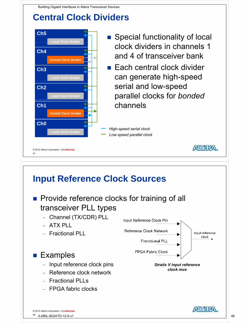
Fractional PLLs
Can serve directly as t itt PLLtransmitter PLL Data rate dependant
Provide increasedfPLL
Ch 5
Ch 4 Provide increased multiplication/division factors over CMU PLLs
fPLLCh 4
Ch 3
Allows full use of device transceiver channels
Ch 2
Ch 1 fPLL Channel PLL can be used as CDR PLLCh 1
Ch 0
fPLL
© 2012 Altera Corporation—Confidential
89
Transmitter Local Clock Dividers
One in each channel
Receive high speed serial clocks from any transmitter PLLtransmitter PLL
Generates High-speed serial clock for local g p
PMA
Low-speed parallel clock for local PMA/PCS
Active in non-bonded(x1) mode
Each channel divides high- Each channel divides high-speed clock to support its individual target data rate
© 2012 Altera Corporation—Confidential
90
Building Gigabit Interfaces in Altera Transceiver Devices
A-MNL-BGIATD-12-0-v1 45
Central Clock Dividers
Special functionality of local Ch5
Local Clock Divider
clock dividers in channels 1 and 4 of transceiver bank
Ch4
Local Clock Divider
Local Clock DividerCentral Clock Divider
Each central clock divider can generate high-speed
Ch3
Local Clock Divider g g pserial and low-speed parallel clocks for bonded
Ch2
Local Clock Divider pchannelsCh1
Local Clock DividerCentral Clock Divider
Ch0
Local Clock DividerHigh-speed serial clock
Low-speed parallel clock
© 2012 Altera Corporation—Confidential
91
Input Reference Clock Sources
Provide reference clocks for training of all transceiver PLL types Channel (TX/CDR) PLL
ATX PLL
Fractional PLL
Examples Input reference clock pins
Reference clock network
Fractional PLLs
Stratix V input reference clock mux
Fractional PLLs
FPGA fabric clocks
© 2012 Altera Corporation—Confidential
92
Building Gigabit Interfaces in Altera Transceiver Devices
A-MNL-BGIATD-12-0-v1 46
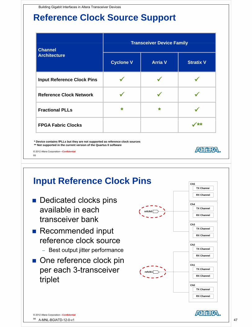
Reference Clock Source Support
Transceiver Device Family
ChannelArchitecture
Transceiver Device Family
Cyclone V Arria V Stratix VCyclone V Arria V Stratix V
Input Reference Clock Pins p
Reference Clock Network
Fractional PLLs * *
FPGA Fabric Clocks **
© 2012 Altera Corporation—Confidential
93
* Device contains fPLLs but they are not supported as reference clock sources** Not supported in the current version of the Quartus II software
Input Reference Clock Pins Ch5
Dedicated clocks pins Ch4
TX Channel
RX Channel
available in each transceiver bank
refclk0TX Channel
RX Channel
Ch3
Recommended input reference clock source
Ch2
TX Channel
RX Channel
Best output jitter performance
One reference clock pin
Ch2
TX Channel
RX Channel
Ch1p
per each 3-transceiver triplet
refclk1
Ch1
TX Channel
RX Channel
pCh0
TX Channel
RX Channel
© 2012 Altera Corporation—Confidential
94
Building Gigabit Interfaces in Altera Transceiver Devices
A-MNL-BGIATD-12-0-v1 47
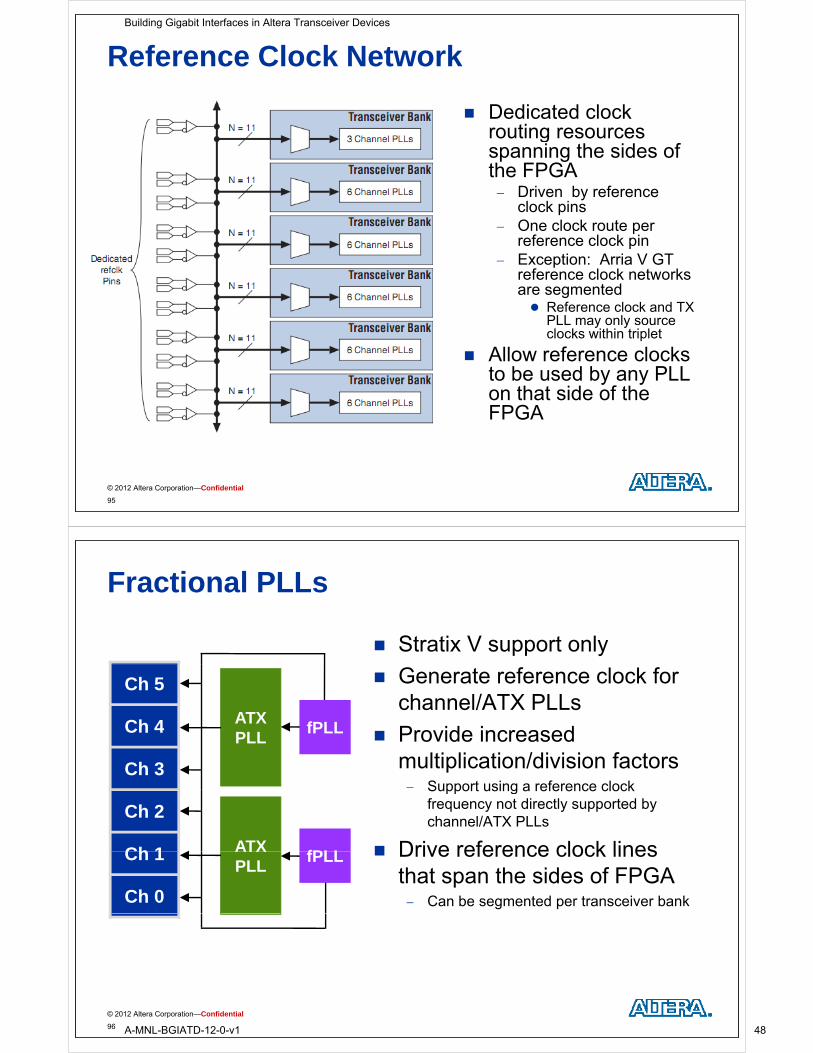
Reference Clock Network
Dedicated clock routing resources gspanning the sides of the FPGA Driven by reference
l k iclock pins One clock route per
reference clock pin Exception: Arria V GTException: Arria V GT
reference clock networks are segmented Reference clock and TX
PLL may only source y yclocks within triplet
Allow reference clocks to be used by any PLL
th t id f thon that side of the FPGA
© 2012 Altera Corporation—Confidential
95
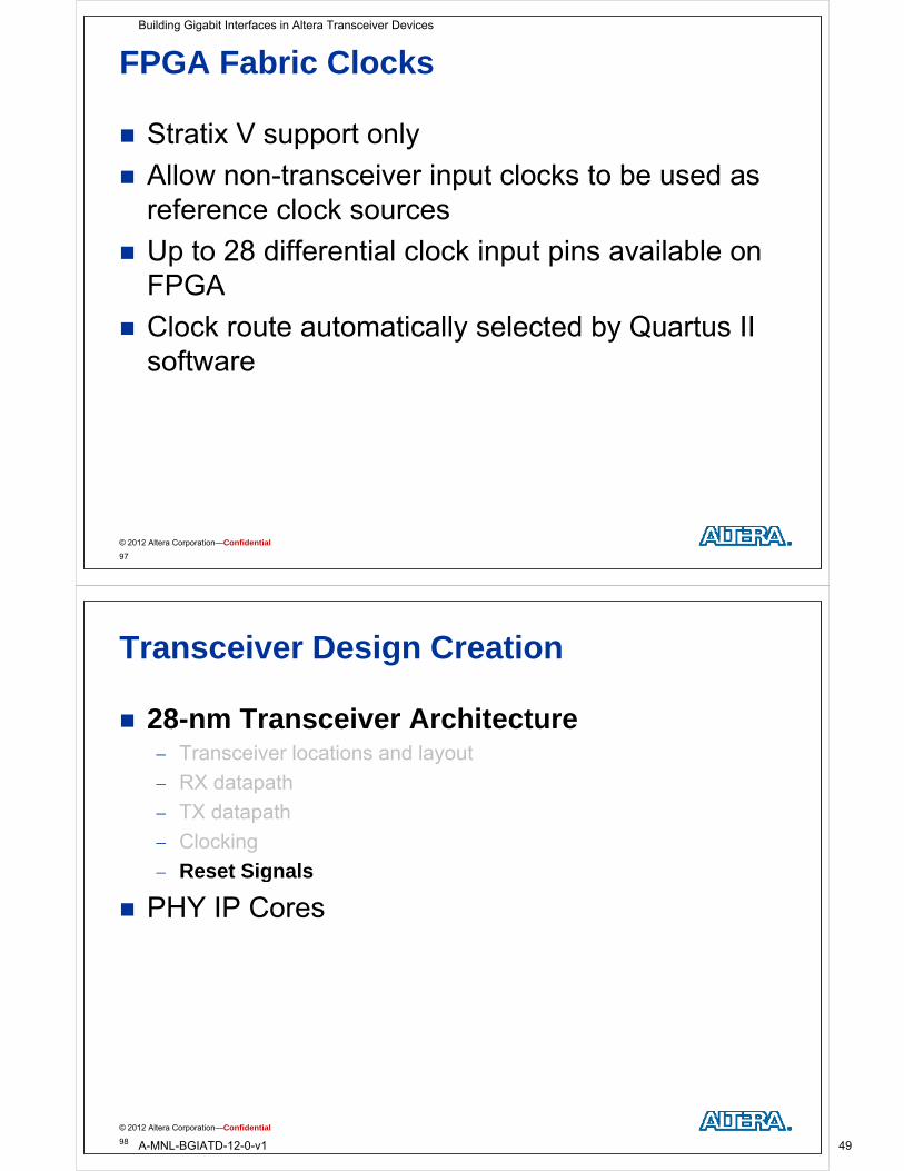
Fractional PLLs
Stratix V support only
Generate reference clock for channel/ATX PLLs
P id i dATX
Ch 5
Ch 4 fPLL Provide increased multiplication/division factors Support using a reference clock
PLLCh 4
Ch 3
fPLL
Support using a reference clock frequency not directly supported by channel/ATX PLLs
Drive reference clock linesATX
Ch 2
Ch 1 fPLL Drive reference clock lines that span the sides of FPGA Can be segmented per transceiver bank
ATX PLL
Ch 1
Ch 0
fPLL
© 2012 Altera Corporation—Confidential
96
Building Gigabit Interfaces in Altera Transceiver Devices
A-MNL-BGIATD-12-0-v1 48
FPGA Fabric Clocks
Stratix V support only
Allow non-transceiver input clocks to be used as reference clock sources
Up to 28 differential clock input pins available on FPGAFPGA
Clock route automatically selected by Quartus II softwaresoftware
© 2012 Altera Corporation—Confidential
97
Transceiver Design Creation
28-nm Transceiver Architecture Transceiver locations and layout
RX datapath
TX datapath TX datapath
Clocking
Reset SignalsReset Signals
PHY IP Cores
© 2012 Altera Corporation—Confidential
98
Building Gigabit Interfaces in Altera Transceiver Devices
A-MNL-BGIATD-12-0-v1 49
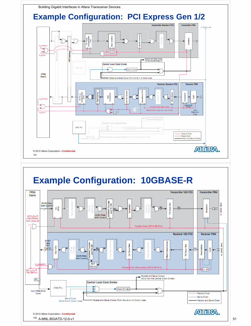
Transceiver Reset Signals
Five different reset signals per transceiver instance
Reset Signal Functionality Default Availability
pll_powerdown Resets CMU and ATX PLLs 1 per transceiver instance
R t RX PMA bl k (i l dirx_analogreset
Resets RX PMA blocks (including CDR)
1 per channel
rx digitalreset Resets RX PCS blocks 1 per channelrx_digitalreset Resets RX PCS blocks 1 per channel
tx_digitalreset Resets TX PCS blocks 1 per channel
tx_analogreset Resets TX PMA blocks 1 per channel
© 2012 Altera Corporation—Confidential
99
Reset Solutions
Embedded Reset ControllerA il bl b d f l i h f h T i PHY IP Available by default with most of the Transceiver PHY IP cores (discussed later)
Avalon® Memory-Mapped reset registers Avalon Memory Mapped reset registers Read and write to control and status registers using embedded
controller to reset channelsA il bl b d f lt ith t f th T i PHY IP Available by default with most of the Transceiver PHY IP cores
Transceiver PHY Reset Controller IP coreAvailable in MegaWizard® Plug In Manager Available in MegaWizard® Plug-In Manager
Custom User designs custom reset logic in the FPGA fabricUser designs custom reset logic in the FPGA fabric Transceiver core provides necessary signals for implementation
© 2012 Altera Corporation—Confidential
100
Building Gigabit Interfaces in Altera Transceiver Devices
A-MNL-BGIATD-12-0-v1 50
Example Configuration: PCI Express Gen 1/2
© 2012 Altera Corporation—Confidential
101
Example Configuration: 10GBASE-R
© 2012 Altera Corporation—Confidential
102
Building Gigabit Interfaces in Altera Transceiver Devices
A-MNL-BGIATD-12-0-v1 51
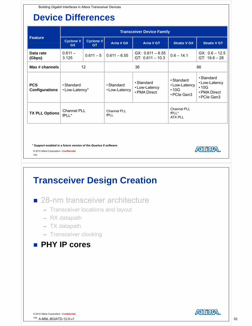
Device Differences
Feature
Transceiver Device Family
Cyclone V Cyclone VArria V GX Arria V GT Stratix V GX Stratix V GT
GX GTArria V GX Arria V GT Stratix V GX Stratix V GT
Data rate (Gbps)
0.611 –3.125
0.611 – 5 0.611 – 6.55GX: 0.611 – 6.55GT: 0.611 – 10.3
0.6 – 14.1GX: 0.6 – 12.5GT: 19.6 – 28
Max # channels 12 36 66
St d d• Standard
• StandardL L t
PCS Configurations
• Standard• Low-Latency*
• Standard• Low-Latency
• Standard• Low-Latency• PMA Direct
Standard• Low-Latency• 10G• PCIe Gen3
• Low-Latency• 10G• PMA Direct• PCIe Gen3
TX PLL OptionsChannel PLLfPLL*
Channel PLLfPLL
Channel PLLfPLL*ATX PLL
© 2012 Altera Corporation—Confidential
103
* Support enabled in a future version of the Quartus II software.
Transceiver Design Creation
28-nm transceiver architecture Transceiver locations and layout
RX datapath
TX datapath TX datapath
Transceiver clocking
PHY IP cores PHY IP cores
© 2012 Altera Corporation—Confidential
104
Building Gigabit Interfaces in Altera Transceiver Devices
A-MNL-BGIATD-12-0-v1 52
Transceiver PHY IP Cores
Set of IP Cores that enable/configure the FPGAs PCS/PMA layers for high-speed designs
Both protocol-specific and generic cores p p gavailable
Implementation Implementation Embedded transceivers
Core logic
Both
© 2012 Altera Corporation—Confidential
105
Non-Protocol-Specific PHY IP Cores
Custom
Low Latency
Deterministic Deterministic
Native
© 2012 Altera Corporation—Confidential
106
Building Gigabit Interfaces in Altera Transceiver Devices
A-MNL-BGIATD-12-0-v1 53
Custom PHY IP Core
Generic PHY for supporting custom interfacesP i t t l Proprietary protocol
No protocol-specific PHY IP available
Supports Standard PCS configuration onlySupports Standard PCS configuration only Contains
PMA and PCS PMA and PCS register map Reset controller (optional) PHY management interfacePHY management interface
Supported devices/data rates Stratix V devices: 0.622 – 8.5 Gbps Arria V devices: 0.622 – 6.5 Gbps Cyclone V GX devices: 0.622 – 3.125 Gbps
© 2012 Altera Corporation—Confidential
107
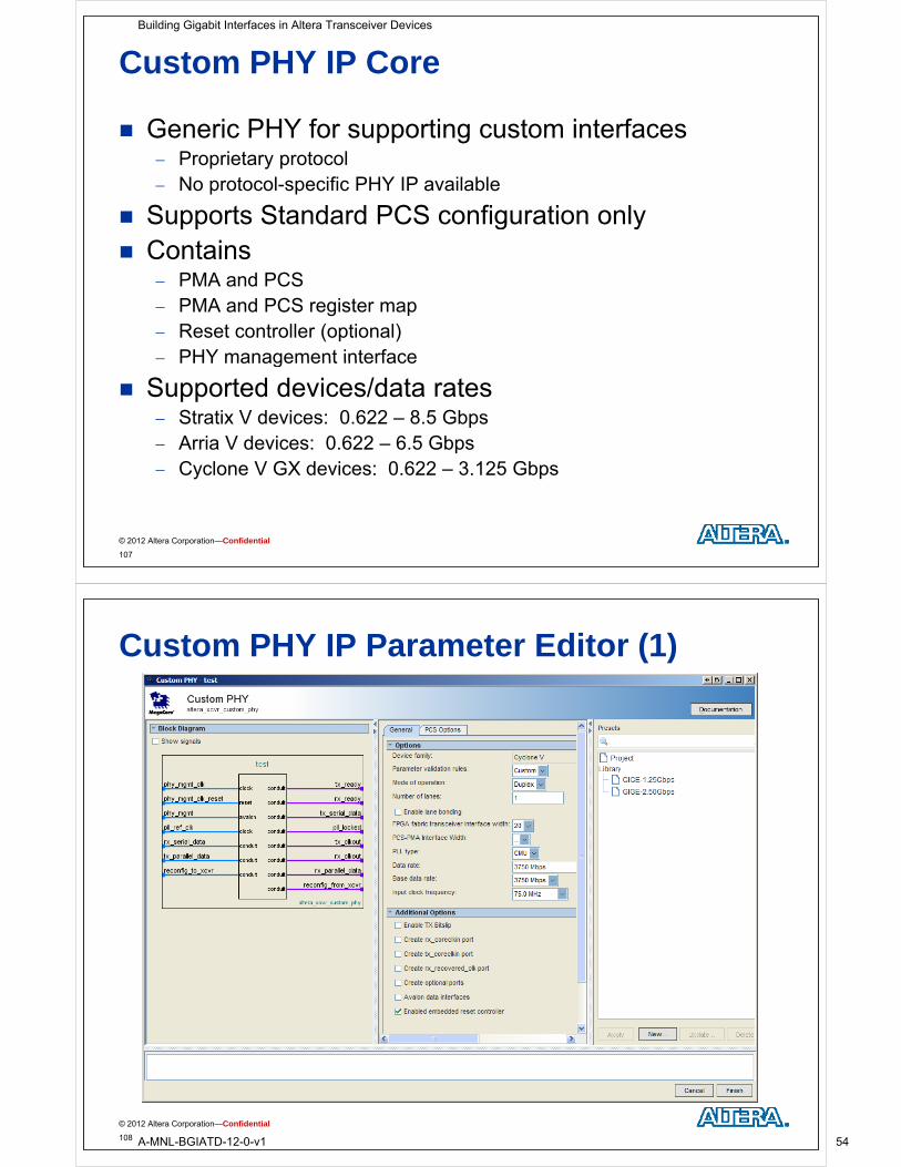
Custom PHY IP Parameter Editor (1)
© 2012 Altera Corporation—Confidential
108
Building Gigabit Interfaces in Altera Transceiver Devices
A-MNL-BGIATD-12-0-v1 54
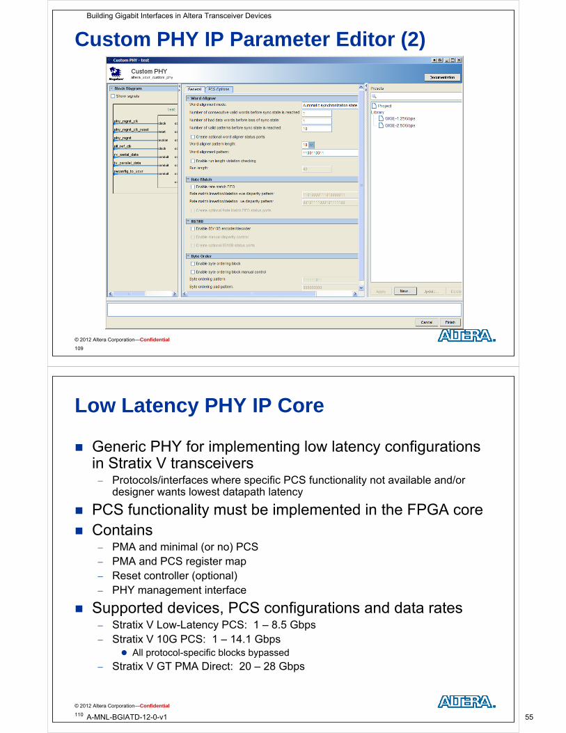
Custom PHY IP Parameter Editor (2)
© 2012 Altera Corporation—Confidential
109
Low Latency PHY IP Core
Generic PHY for implementing low latency configurations in Stratix V transceiversin Stratix V transceivers Protocols/interfaces where specific PCS functionality not available and/or
designer wants lowest datapath latency
PCS f ti lit t b i l t d i th FPGA PCS functionality must be implemented in the FPGA core Contains
PMA and minimal (or no) PCSPMA and minimal (or no) PCS PMA and PCS register map Reset controller (optional) PHY management interfacePHY management interface
Supported devices, PCS configurations and data rates Stratix V Low-Latency PCS: 1 – 8.5 Gbps
St ti V 10G PCS 1 14 1 Gb Stratix V 10G PCS: 1 – 14.1 Gbps All protocol-specific blocks bypassed
Stratix V GT PMA Direct: 20 – 28 Gbps
© 2012 Altera Corporation—Confidential
110
Building Gigabit Interfaces in Altera Transceiver Devices
A-MNL-BGIATD-12-0-v1 55
Low Latency PHY IP Parameter Editor
© 2012 Altera Corporation—Confidential
111
Deterministic PHY IP Core
Generic PHY for protocols/interfaces that have a TX/RX datapath latency variation requirementTX/RX datapath latency variation requirement Supports auto-rate configuration
Enables select blocks/modes in the Standard PCS fi ticonfiguration
ContainsPMA and PCS PMA and PCS
PMA and PCS register map Reset controller (optional)
PHY management interface PHY management interface
Supported devices/data rates Stratix V devices: 0.6 – 11 Gbps Arria V devices: 0.6 – 6 Gbps
© 2012 Altera Corporation—Confidential
112
Building Gigabit Interfaces in Altera Transceiver Devices
A-MNL-BGIATD-12-0-v1 56
Deterministic PHY IP Parameter Editor
© 2012 Altera Corporation—Confidential
113
Custom/Low Latency/Deterministic PHY IP Block Diagram
tx_serial_datarx serial data
Serial DataAvalon-ST RX/TXtx_*rx * rx_serial_datarx_
tx_readyrx_ready
pll lockedPCS/PMAControl & Statuspll ref clk pll_locked
…Control & Status
reconfig_* Reconfiguration
pll_ref_clk*_coreclkin
Clocks
phy_mgmt_*Avalon-MM
PHY Management
pll_powerdown*_analogreset* digitalreset
Reset Control & Status (Optional)_digitalreset
© 2012 Altera Corporation—Confidential
114
Building Gigabit Interfaces in Altera Transceiver Devices
A-MNL-BGIATD-12-0-v1 57
Custom/Low Latency/Deterministic PHY IP Interfaces Clock interfaces
To reference clock sources To MAC To any additional PCS blocks implemented in FPGA (as needed)To any additional PCS blocks implemented in FPGA (as needed)
Avalon-ST TX/RX interfaces – to MAC Serial data interface – to external channel Avalon-MM PHY management interface – to MAC or
PCS/PMA control logicT i fi ti i t f t Transceiver reconfiguration interface – to reconfiguration controller
Reset control and status – reset control logic Reset control and status reset control logic PCS/PMA control and status (optional) – to MAC or
PHY control logic
© 2012 Altera Corporation—Confidential
115
Clock Interfaces
pll_ref_clk: Input reference clock(s) tx_clkout: Output clock from PHY to use for
synchronizing TX output data, control and status i lsignals
rx_clkout: Output clock from PHY; synchronized t RX d t t l d t t i lto RX data, control and status signals
tx_coreclkin: Optional write-side transmitter h ti FIFO i t l kphase compensation FIFO input clock
rx_coreclkin: Optional read-side receiver phase ti FIFO i t l kcompensation FIFO input clock
© 2012 Altera Corporation—Confidential
116
Building Gigabit Interfaces in Altera Transceiver Devices
A-MNL-BGIATD-12-0-v1 58
Avalon-ST Input/Ouput Interfaces
Standard Altera streaming interface Connects MAC to Custom PHY IP core Implements simple Avalon-ST interface with no
backpressure or latency Interface is always ready to send/receive data
Logic must be ready to send/receive as soon as reset is complete Logic must be ready to send/receive as soon as reset is complete
Transmit signalstx parallel data: Outgoing input data to PHY tx_parallel_data: Outgoing input data to PHY
Receive signals rx parallel data: Incoming output data from PHYrx_parallel_data: Incoming output data from PHY
© 2012 Altera Corporation—Confidential
117
* For more information on the Avalon specification, please see the Avalon Interface Specification .
Serial Interface
Connects transmitter data output(s) and receiver data input(s) to external serial interface Backplane
Physical medium dependent (PMD) interface
Another FPGA
Signals Signals tx_serial_data: Transmitter data output
rx serial data: Receiver data input rx_serial_data: Receiver data input
© 2012 Altera Corporation—Confidential
118
Building Gigabit Interfaces in Altera Transceiver Devices
A-MNL-BGIATD-12-0-v1 59
Altera-MM PHY Management Interface
Standard Altera memory mapped interface 32-bit data, 9-bit address,
phy_mgmt_clk, phy_mgmt_clk_reset, phy_mgmt_address, phy_mgmt_writedata, phy_mgmt_readdata, phy_mgmt_write, phy_mgmt_read, phy_mgmt_watirequest
Use read/write transactions to access register space
Provides a memory-mapped register space used by embedded controllers to access
PCS/PMA control and status registers PCS/PMA control and status registers Reset control registers Transceiver reconfiguration registers
Example control/status registers PLL locked status Reset RX/TX channel Bit/byte reversal FIFO overflow/underflow
© 2012 Altera Corporation—Confidential
119
Note: See Altera Transceiver PHY IP Core User Guide for register mapping.
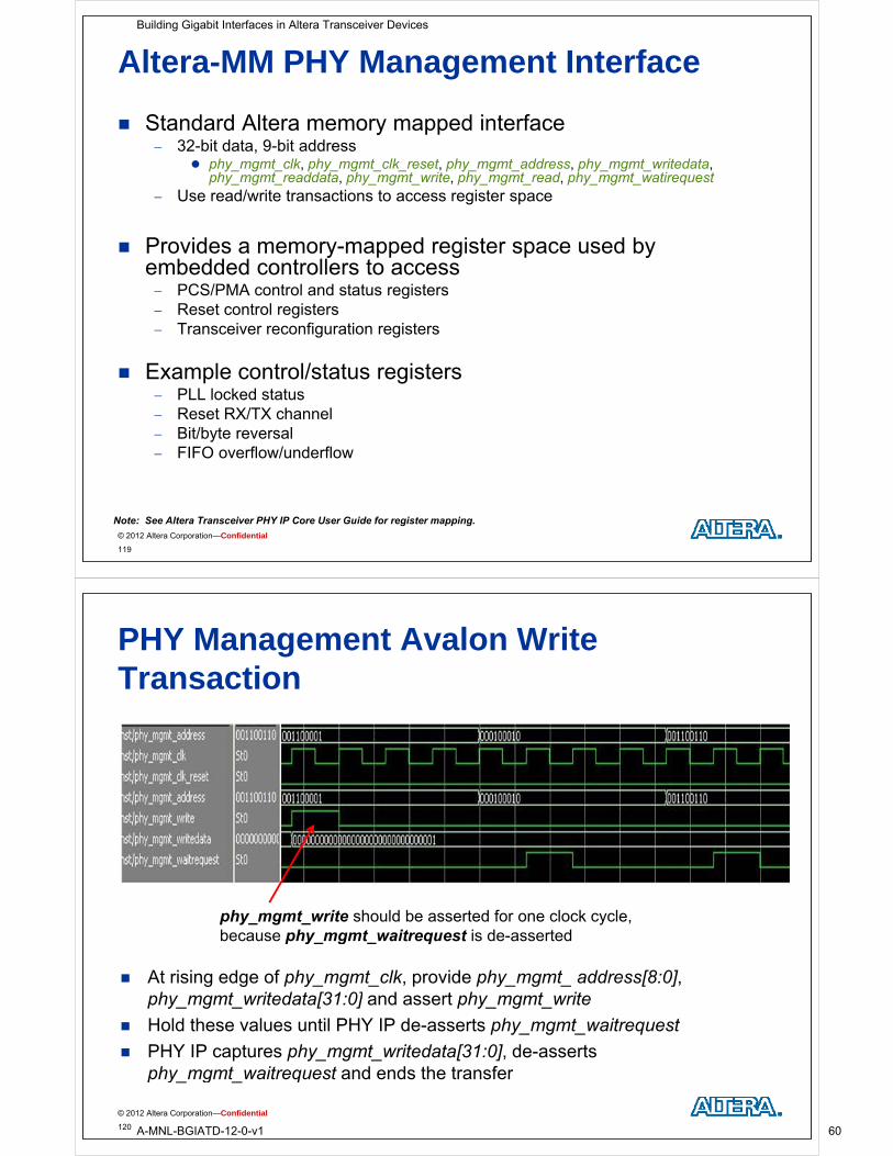
PHY Management Avalon Write Transaction
phy_mgmt_write should be asserted for one clock cycle, because phy mgmt waitrequest is de asserted
At rising edge of phy_mgmt_clk, provide phy_mgmt_ address[8:0], phy mgmt writedata[31:0] and assert phy mgmt write
because phy_mgmt_waitrequest is de-asserted
phy_mgmt_writedata[31:0] and assert phy_mgmt_write
Hold these values until PHY IP de-asserts phy_mgmt_waitrequest
PHY IP captures phy_mgmt_writedata[31:0], de-asserts phy mgmt waitrequest and ends the transfer
© 2012 Altera Corporation—Confidential
phy_mgmt_waitrequest and ends the transfer
120
Building Gigabit Interfaces in Altera Transceiver Devices
A-MNL-BGIATD-12-0-v1 60
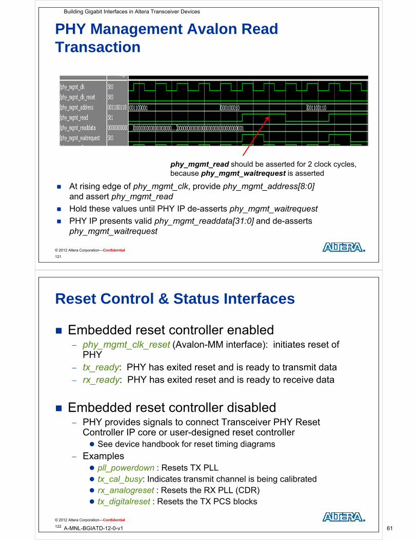
PHY Management Avalon Read Transaction
phy mgmt read should be asserted for 2 clock cycles,
At rising edge of phy_mgmt_clk, provide phy_mgmt_address[8:0] and assert phy mgmt read
p y_ g _ y ,because phy_mgmt_waitrequest is asserted
and assert phy_mgmt_read
Hold these values until PHY IP de-asserts phy_mgmt_waitrequest
PHY IP presents valid phy_mgmt_readdata[31:0] and de-asserts phy mgmt waitrequest
© 2012 Altera Corporation—Confidential
phy_mgmt_waitrequest
121
Reset Control & Status Interfaces
Embedded reset controller enabledh lk (A l MM i f ) i i i f phy_mgmt_clk_reset (Avalon-MM interface): initiates reset of
PHY tx_ready: PHY has exited reset and is ready to transmit data rx_ready: PHY has exited reset and is ready to receive data
E b dd d t t ll di bl d Embedded reset controller disabled PHY provides signals to connect Transceiver PHY Reset
Controller IP core or user-designed reset controllerg See device handbook for reset timing diagrams
Examples pll powerdown : Resets TX PLL pll_powerdown : Resets TX PLL tx_cal_busy: Indicates transmit channel is being calibrated rx_analogreset : Resets the RX PLL (CDR) tx digitalreset : Resets the TX PCS blocks
© 2012 Altera Corporation—Confidential
tx_digitalreset : Resets the TX PCS blocks
122
Building Gigabit Interfaces in Altera Transceiver Devices
A-MNL-BGIATD-12-0-v1 61
Optional PCS/PMA Control and Status Interface Additional signals to determine and control state of g
PCS/PMA Provides instantaneous interaction over using PHY
management interfacemanagement interface Examples
tx datak: Input to indicate data/control code (8B/10B encoding )
_ p ( genabled)
rx_syncstatus : Indicates single-lane word alignment rx_rmfifodatainserted : Indicates Rate Match has inserted skip
charactercharacter rx_errdetect : Indicates an 8B/10B code violation or disperity error
has occurredtx rlv: Indicates a run length violation has occurred in the receiver tx_rlv: Indicates a run length violation has occurred in the receiver
rx_datak: Data/control code indicator (8B/10B decoding enabled) rx_runningdisp: Indicates disparity of incoming data (8B/10B
decoding enabled)
© 2012 Altera Corporation—Confidential
rx_enabyteordflag: Triggers byte ordering
123
Native PHY IP Cores
Low-level generic PHY IP cores for supporting custom and standard protocols All legal transceiver settings/features are made available to
designerdesigner
Most flexible of the PHY IP cores
Two current versions Stratix V Transceiver Native PHY IP core
A i V T i N ti PHY IP Arria V Transceiver Native PHY IP core
© 2012 Altera Corporation—Confidential
124
Building Gigabit Interfaces in Altera Transceiver Devices
A-MNL-BGIATD-12-0-v1 62
Native PHY IP Cores
All PHY control/status signals exposed as ports Similar to enabling “all optional ports” on other PHY IP cores
No memory-mapped register interface to control and monitor PHY
Must build own “register space” using ports to access in memory Must build own “register-space” using ports to access in memory-mapped system (if required)
Contains PHY (PCS/PMA) only Contains PHY (PCS/PMA) only Reconfiguration controller must be connected manually
Reset controller must be connected manuallyy Designer can use Transceiver PHY Reset Controller IP core or
create own reset controller
S t l PMA Di t d * Supports only PMA Direct mode* All PCS functionality must be implemented in FPGA core
© 2012 Altera Corporation—Confidential
125
* Other modes enabled in a future version of the Quartus II software
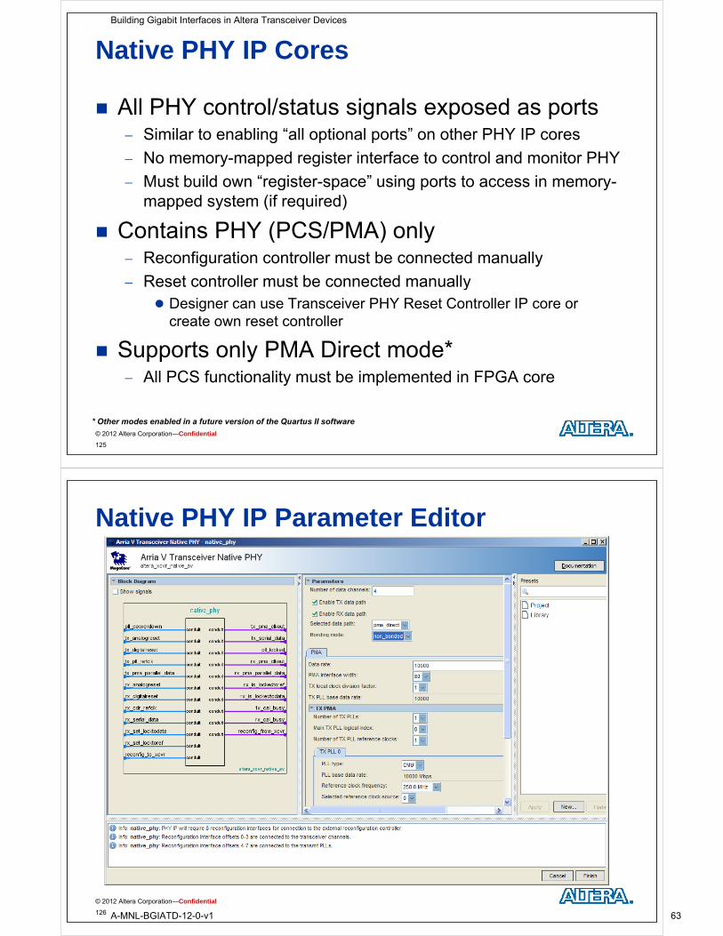
Native PHY IP Parameter Editor
© 2012 Altera Corporation—Confidential
126
Building Gigabit Interfaces in Altera Transceiver Devices
A-MNL-BGIATD-12-0-v1 63
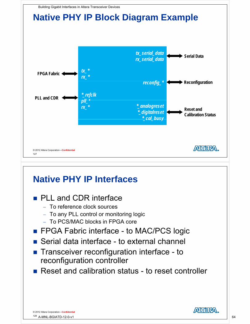
Native PHY IP Block Diagram Example
tx_serial_datarx_serial_data
Serial Data
FPGA Fabrictx_*rx_*
fi * R fi tireconfig_* Reconfiguration
*_refclkpll *
PLL and CDR
*_analogreset*_digitalreset
* cal busy
Reset and Calibration Status
pll_*rx_*
_cal_busy
© 2012 Altera Corporation—Confidential
127
Native PHY IP Interfaces
PLL and CDR interfaceT f l k To reference clock sources
To any PLL control or monitoring logic To PCS/MAC blocks in FPGA core
FPGA Fabric interface - to MAC/PCS logic Serial data interface - to external channel Serial data interface to external channel Transceiver reconfiguration interface - to
reconfiguration controllerreconfiguration controller Reset and calibration status - to reset controller
© 2012 Altera Corporation—Confidential
128
Building Gigabit Interfaces in Altera Transceiver Devices
A-MNL-BGIATD-12-0-v1 64
Clock Interfaces
tx_pll_refclk: Input reference clock(s) for TX PLL(s) rx cdr refclk: Input reference clock(s) for RX rx_cdr_refclk: Input reference clock(s) for RX
CDR(s) tx pma clkout: Output clock from PHYtx_pma_clkout: Output clock from PHY
Use to drive TX PCS and synchronize outgoing TX output data
rx_pma_clkout: Output clock from PHYU t d i RX PCS RX d t i h i d t thi l k Use to drive RX PCS as RX data is synchronized to this clock
Additional PLL/CDR control and monitoring signals (examples)( p ) pll_locked: Indicates TX PLL is locked to reference clock rx_is_lockedtoref: Indicates CDR is locked to reference clock rx set lockedtodata: Switches CDR to locked to incoming datarx_set_lockedtodata: Switches CDR to locked to incoming data
mode
© 2012 Altera Corporation—Confidential
129
Remaining Interfaces
Similar to corresponding interfaces on other generic PHY IP cores
No embedded controller tx ready/rx ready not provided_ y _ y p
Must connect individual reset control and status signals to Transceiver Reset Controller PHY or custom reset controller
© 2012 Altera Corporation—Confidential
130
Building Gigabit Interfaces in Altera Transceiver Devices
A-MNL-BGIATD-12-0-v1 65
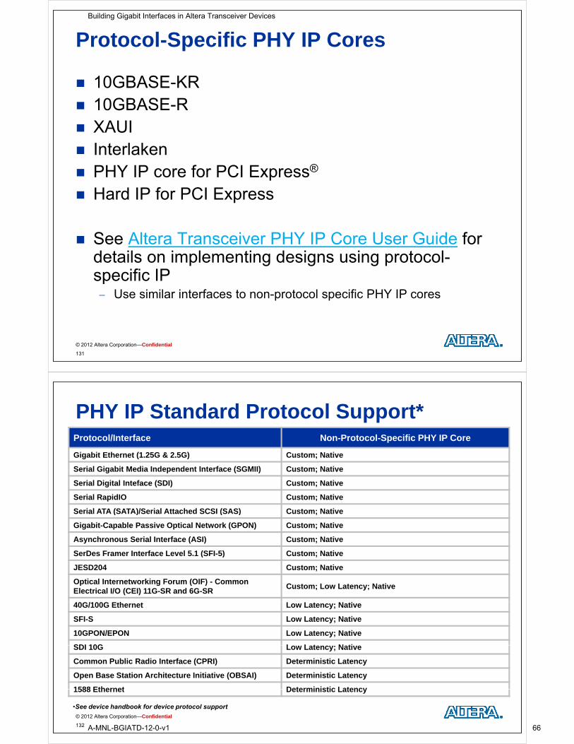
Protocol-Specific PHY IP Cores
10GBASE-KR10GBASE R 10GBASE-R
XAUI Interlaken PHY IP core for PCI Express®
Hard IP for PCI Express
See Altera Transceiver PHY IP Core User Guide for details on implementing designs using protocol-specific IPspecific IP Use similar interfaces to non-protocol specific PHY IP cores
© 2012 Altera Corporation—Confidential
131
PHY IP Standard Protocol Support*Protocol/Interface Non-Protocol-Specific PHY IP Core
Gigabit Ethernet (1.25G & 2.5G) Custom; Native
Serial Gigabit Media Independent Interface (SGMII) Custom; NativeSerial Gigabit Media Independent Interface (SGMII) Custom; Native
Serial Digital Inteface (SDI) Custom; Native
Serial RapidIO Custom; Native
Serial ATA (SATA)/Serial Attached SCSI (SAS) Custom; NativeSerial ATA (SATA)/Serial Attached SCSI (SAS) Custom; Native
Gigabit-Capable Passive Optical Network (GPON) Custom; Native
Asynchronous Serial Interface (ASI) Custom; Native
SerDes Framer Interface Level 5.1 (SFI-5) Custom; Native( )
JESD204 Custom; Native
Optical Internetworking Forum (OIF) - Common Electrical I/O (CEI) 11G-SR and 6G-SR
Custom; Low Latency; Native
40G/100G Ethernet Low Latency; Native
SFI-S Low Latency; Native
10GPON/EPON Low Latency; Native
SDI 10G L L t N tiSDI 10G Low Latency; Native
Common Public Radio Interface (CPRI) Deterministic Latency
Open Base Station Architecture Initiative (OBSAI) Deterministic Latency
1588 Ethernet Deterministic Latency
© 2012 Altera Corporation—Confidential
132
1588 Ethernet Deterministic Latency
•See device handbook for device protocol support
Building Gigabit Interfaces in Altera Transceiver Devices
A-MNL-BGIATD-12-0-v1 66
PHY IP Output Files for Compilation
<phy_instance_name>.qipS i t fil th t i t t ll fil d d f th i Script file that points to all files needed for synthesis
Add file to Quartus II project
<phy instance name>.v/.vhdphy_instance_name .v/.vhd Wrapper file that instantiates and configures the PHY IP core
megafunction
<ph instance name> folder <phy_instance_name> folder Combination of Verilog and SystemVerilog files representing PHY IP
core components
<phy_instance_name>.ppf Stores top-level I/O and node information for importing into Pin
PlannerPlanner Useful when pin layout must be assigned before top-level file is
completed
© 2012 Altera Corporation—Confidential
133
Qsys and PHY IP Cores
PHY IP cores not available in Qsys Component LibraryLibrary Similar PCI Express, Interlaken, Ethernet and RapidIO® solutions are
available
To incorporate PHY IP into Qsys system Create custom component using PHY IP core instance
Works for cores that use mostly Avalon interfaces Works for cores that use mostly Avalon interfaces e.g. Custom, Low-Latency and Deterministic PHY IP cores
Export non-Avalon interfaces out of Qsys system
Build a custom component bridge (signal mapper) for communication Build a custom component bridge (signal mapper) for communication with PHY IP core and instantiate PHY IP core outside Qsys system Use for cores that employ mostly non-Avalon interfaces
e g Native PHY IP coree.g. Native PHY IP core
Must design custom register map logic to access transceiver control/status signals
© 2012 Altera Corporation—Confidential
134
Building Gigabit Interfaces in Altera Transceiver Devices
A-MNL-BGIATD-12-0-v1 67
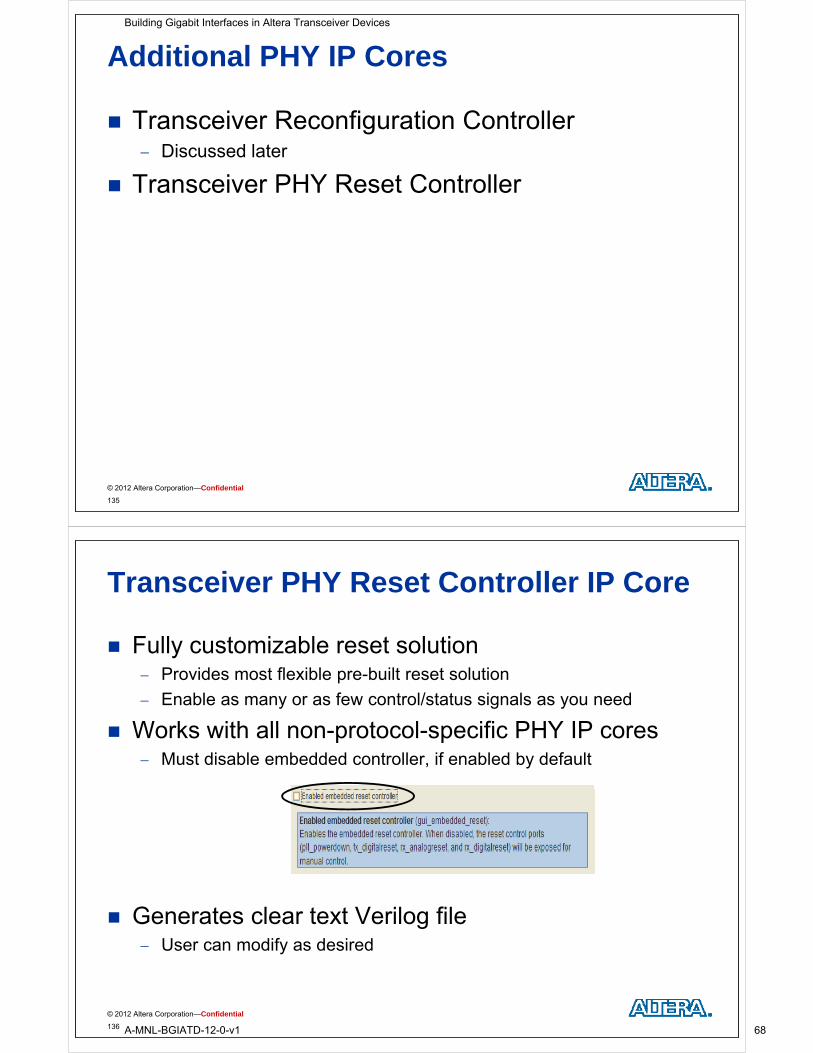
Additional PHY IP Cores
Transceiver Reconfiguration Controller Discussed later
Transceiver PHY Reset Controller
© 2012 Altera Corporation—Confidential
135
Transceiver PHY Reset Controller IP Core
Fully customizable reset solution Provides most flexible pre-built reset solution
Enable as many or as few control/status signals as you need
Works with all non protocol specific PHY IP cores Works with all non-protocol-specific PHY IP cores Must disable embedded controller, if enabled by default
Generates clear text Verilog file Generates clear text Verilog file User can modify as desired
© 2012 Altera Corporation—Confidential
136
Building Gigabit Interfaces in Altera Transceiver Devices
A-MNL-BGIATD-12-0-v1 68

Reset Controller Options
Shared or individual reset controls per channel in transceiver instance
Shared or separate reset controls per each RX p pchannel
Shared or separate reset controls per each TX Shared or separate reset controls per each TX channel
Option for manual or automatic RX/TX reset Option for manual or automatic RX/TX reset recovery when PLLs lose lock
C fi bl ti i d l Configurable timing delay
© 2012 Altera Corporation—Confidential
137
Reset Controller Parameter Editor
© 2012 Altera Corporation—Confidential
138
Building Gigabit Interfaces in Altera Transceiver Devices
A-MNL-BGIATD-12-0-v1 69
Test Your Knowledge
1. What are the 4 non-protocol specific PHY IP?
A. Custom, Low-Latency, Deterministic and Native
2. If the embedded reset controller is disabled in a PHY IP core, what must a designer do?
A. Connect the PHY Reset Controller IP or custom reset control logic
3. What are some of the protocols/interfaces with their own PHY IP cores?
A. 10GBASE-KR, 10GBASE-R, PCI Express, Interlaken, XAUI
© 2012 Altera Corporation—Confidential
139
Please go to Exercise 1g
© 2012 Altera Corporation—Confidential
140
Building Gigabit Interfaces in Altera Transceiver Devices
A-MNL-BGIATD-12-0-v1 70

Building Gigabit Interfaces inBuilding Gigabit Interfaces in Altera Transceiver DevicesMAC/PCS V ifi tiMAC/PCS Verification
© 2012 Altera Corporation—Confidential
MAC/PCS Verification
RTL Simulation
In-System Debugging
© 2012 Altera Corporation—Confidential
142
Building Gigabit Interfaces in Altera Transceiver Devices
A-MNL-BGIATD-12-0-v1 71
RTL Simulation
Simulate PCS/PMA functionality in popular simulators Support for Mentor Graphics®, Cadence and Synopsys® tools
All files needed for PHY IP core simulation generated by MegaWizard manager
User must write test vectors/testbench May use Custom PHY simulation testbench found on Altera Wiki
as starting point or model for Custom and Low-Latency PHY IP simulations
© 2012 Altera Corporation—Confidential
143
PHY IP Output Files for Simulation
All files located in <phy_instance_name>_sim folder located in the Quartus II project directoryQ p j y Must compile all generated files for each PHY IP core in target simulation tool
<phy instance name> v/ vhd <phy_instance_name>.v/.vhd Wrapper file that instantiates and configures the PHY IP core simulation model
files
altera xcvr <phy instance name> subfolder_ _ p y_ _ Directory containing Verilog and SystemVerilog simulation model files needed for
any tool VHDL simulation requires mixed-language simulation tool or ModelSim-Altera tool
cadence mentor and synopsys subfolders cadence, mentor and synopsys subfolders Contains example simulation script files for compiling and simulating PHY IP core
in target simulation tools Modify as needed to simulate entire FPGA or incorporate in the system simulation y y
script
© 2012 Altera Corporation—Confidential
144
Building Gigabit Interfaces in Altera Transceiver Devices
A-MNL-BGIATD-12-0-v1 72

MAC/PCS Verification
RTL Simulation
In-System Debugging SignalTap® II embedded logic analyzer (ELA)
In-System Sources and Probes
In-System Memory Content Editor
S t C l System Console
© 2012 Altera Corporation—Confidential
145
SignalTap II Embedded Logic Analyzer
Captures the logic state of FPGA internal signals using a defined clock signaldefined clock signal
Connects to Quartus II software through FPGA JTAG connection
Gives designers ability to monitor buried signals Captures real-time data on rising edges of sampling clock
© 2012 Altera Corporation—Confidential
146
Building Gigabit Interfaces in Altera Transceiver Devices
A-MNL-BGIATD-12-0-v1 73
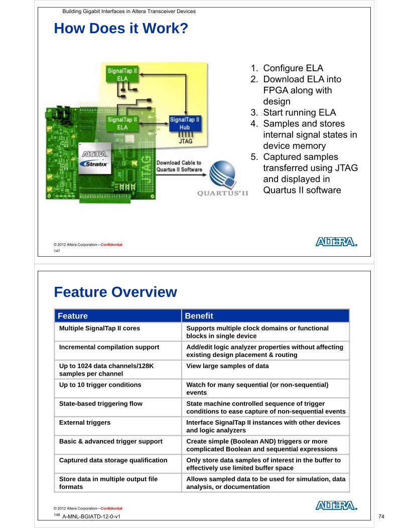
How Does it Work?
1 Configure ELA1. Configure ELA2. Download ELA into
FPGA along with designdesign
3. Start running ELA4. Samples and stores
i t l i l t t iinternal signal states in device memory
5. Captured samples transferred using JTAG and displayed in Quartus II software
© 2012 Altera Corporation—Confidential
147
Feature Overview
Feature Benefit
Multiple SignalTap II cores Supports multiple clock domains or functional blocks in single device
Incremental compilation support Add/edit logic analyzer properties without affecting existing design placement & routing
U t 1024 d t h l /128K Vi l l f d tUp to 1024 data channels/128K samples per channel
View large samples of data
Up to 10 trigger conditions Watch for many sequential (or non-sequential) events
State-based triggering flow State machine controlled sequence of trigger conditions to ease capture of non-sequential events
External triggers Interface SignalTap II instances with other devices and logic analyzers
Basic & advanced trigger support Create simple (Boolean AND) triggers or more complicated Boolean and sequential expressions
C t d d t t lifi ti O l t d t l f i t t i th b ff tCaptured data storage qualification Only store data samples of interest in the buffer to effectively use limited buffer space
Store data in multiple output file formats
Allows sampled data to be used for simulation, data analysis, or documentation
© 2012 Altera Corporation—Confidential
148
y ,
Building Gigabit Interfaces in Altera Transceiver Devices
A-MNL-BGIATD-12-0-v1 74
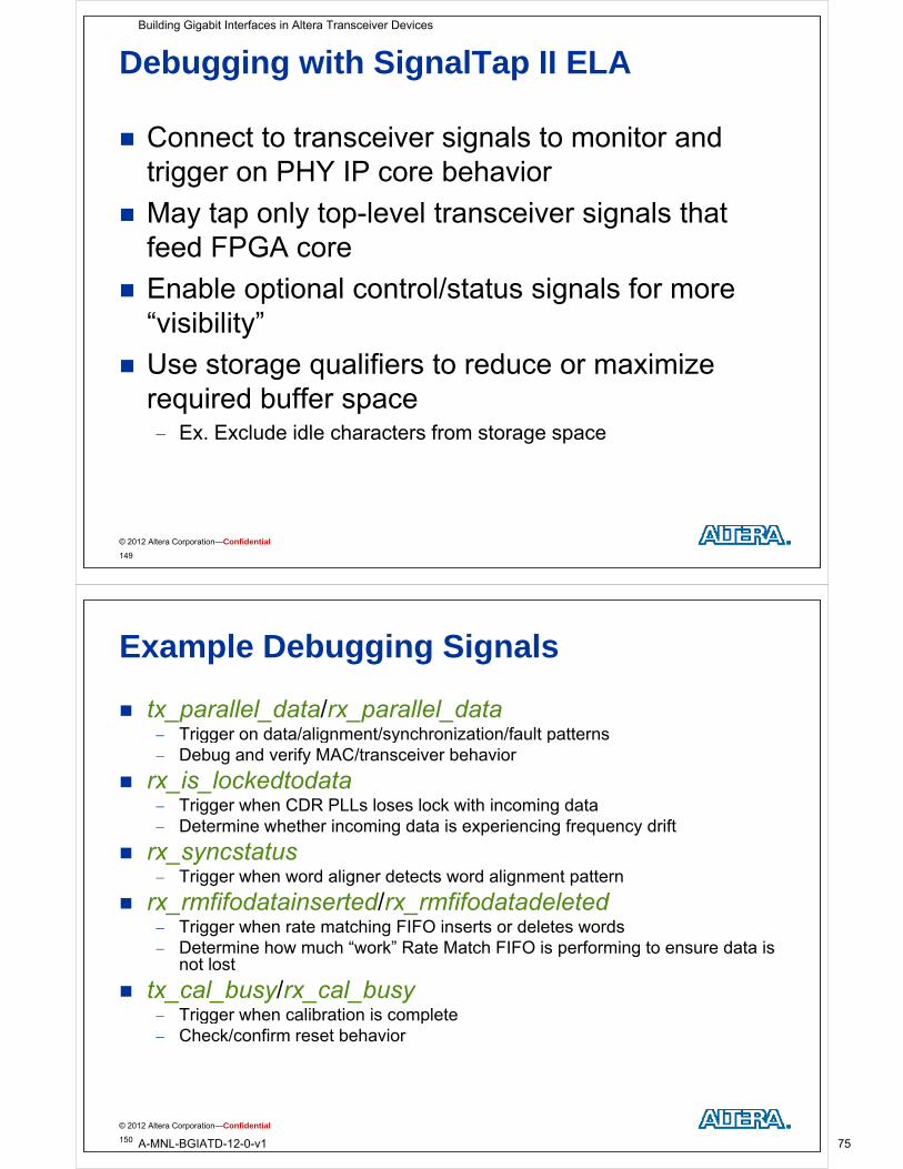
Debugging with SignalTap II ELA
Connect to transceiver signals to monitor and trigger on PHY IP core behavior
May tap only top-level transceiver signals that y p y p gfeed FPGA core
Enable optional control/status signals for more Enable optional control/status signals for more “visibility”
Use storage qualifiers to reduce or maximize Use storage qualifiers to reduce or maximize required buffer space
Ex Exclude idle characters from storage space Ex. Exclude idle characters from storage space
© 2012 Altera Corporation—Confidential
149
Example Debugging Signals
tx_parallel_data/rx_parallel_data Trigger on data/alignment/synchronization/fault patternsTrigger on data/alignment/synchronization/fault patterns Debug and verify MAC/transceiver behavior
rx_is_lockedtodata Trigger when CDR PLLs loses lock with incoming data Trigger when CDR PLLs loses lock with incoming data Determine whether incoming data is experiencing frequency drift
rx_syncstatusTrigger when word aligner detects word alignment pattern Trigger when word aligner detects word alignment pattern
rx_rmfifodatainserted/rx_rmfifodatadeleted Trigger when rate matching FIFO inserts or deletes words
Determine how much “work” Rate Match FIFO is performing to ensure data is Determine how much work Rate Match FIFO is performing to ensure data is not lost
tx_cal_busy/rx_cal_busyTrigger when calibration is complete Trigger when calibration is complete
Check/confirm reset behavior
© 2012 Altera Corporation—Confidential
150
Building Gigabit Interfaces in Altera Transceiver Devices
A-MNL-BGIATD-12-0-v1 75
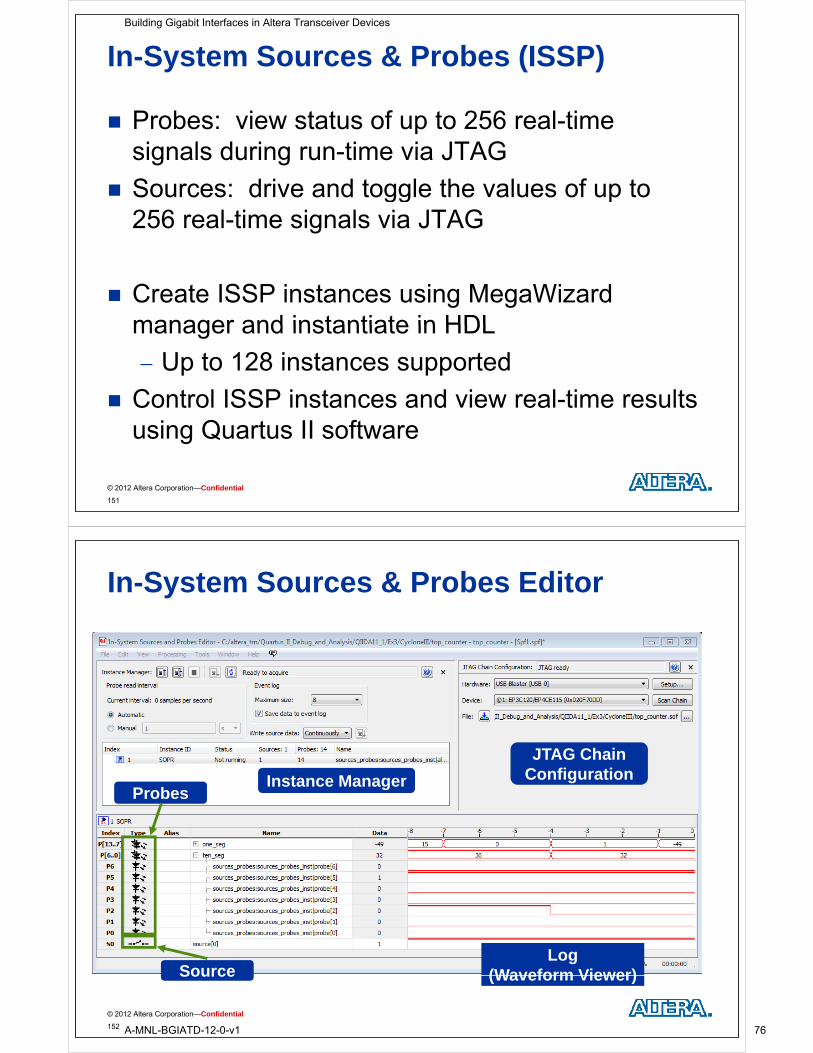
In-System Sources & Probes (ISSP)
Probes: view status of up to 256 real-time signals during run-time via JTAG
Sources: drive and toggle the values of up to gg p256 real-time signals via JTAG
Create ISSP instances using MegaWizardmanager and instantiate in HDLmanager and instantiate in HDL
Up to 128 instances supported
Control ISSP instances and view real-time results using Quartus II software
© 2012 Altera Corporation—Confidential
151
In-System Sources & Probes Editor
JTAG Chain ConfigurationInstance Manager
P bg
Probes
Log(Waveform Viewer)Source
© 2012 Altera Corporation—Confidential
152
(Waveform Viewer)Source
Building Gigabit Interfaces in Altera Transceiver Devices
A-MNL-BGIATD-12-0-v1 76
Debugging with ISSP
Control and monitor transceiver behavior without having to recode control logic Limitation: JTAG performance
Examplesp Force transceiver reset or re-calibration
Manually force error conditions to occur
Extensive Tcl scripting support to allow creation of custom automated design control interfaces
Force trigger conditions for debugging design with the SignalTapForce trigger conditions for debugging design with the SignalTap II Embedded Logic Analyzer
© 2012 Altera Corporation—Confidential
153
In-System Memory Content Editor (ISMCE)
Allows Viewing contents of memories & constants via JTAG
Updating contents of memories & constants via JTAG
Without recompilation or reconfiguration of FPGA
© 2012 Altera Corporation—Confidential
154
Building Gigabit Interfaces in Altera Transceiver Devices
A-MNL-BGIATD-12-0-v1 77
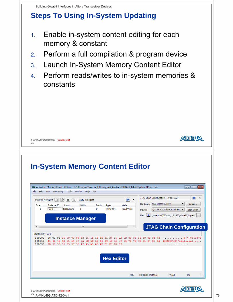
Steps To Using In-System Updating
1. Enable in-system content editing for each memory & constant
2. Perform a full compilation & program devicep p g
3. Launch In-System Memory Content Editor
4 Perform reads/writes to in system memories &4. Perform reads/writes to in-system memories & constants
© 2012 Altera Corporation—Confidential
155
In-System Memory Content Editor
JTAG Chain Configuration
Instance Manager
JTAG Chain Configuration
Hex Editor
© 2012 Altera Corporation—Confidential
156
Building Gigabit Interfaces in Altera Transceiver Devices
A-MNL-BGIATD-12-0-v1 78
Debugging with Memory Content Editor
View and update data values stored in b dd dembedded memory
Examples Monitor high-speed packet data stored in embedded memory
during system testingduring system testing e.g. packet generator/checker data
Insert data errors to determine system reliability
Note: Supported only on single-port memory configurations
© 2012 Altera Corporation—Confidential
157
System Console
Provides low-level system-level debug of Qsyssystem Use JTAG or TCP/IP communication channels
C t t d i t t ith d Connect to and interact with memory mapped or streaming interfaces/components
No processor required No processor required
Interactive Tcl Console Opens as a separate GUI window or in the Nios® II Command Opens as a separate GUI window or in the Nios II Command
Shell
Run individual Tcl commands or automate with Tcl script files
© 2012 Altera Corporation—Confidential
158
Building Gigabit Interfaces in Altera Transceiver Devices
A-MNL-BGIATD-12-0-v1 79
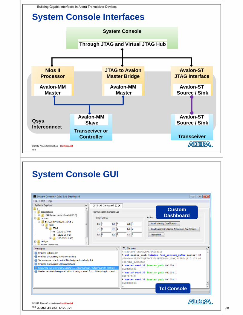
System Console Interfaces
System ConsoleSystem Console
Through JTAG and Virtual JTAG Hub
Avalon-ST JTAG Interface
Avalon-ST JTAG Interface
JTAG to Avalon Master Bridge
JTAG to Avalon Master Bridge
Nios II Processor
Nios II Processor gg
Avalon-MMMaster
Avalon-MMMaster
Avalon-STSource / Sink
A alon MM A alon STQsysInterconnect
Transceiver or Transceiver or
Avalon-MMSlave
Avalon-STSource / Sink
© 2012 Altera Corporation—Confidential
159
ControllerController TransceiverTransceiver
System Console GUI
Custom Dashboard
Tcl Console
© 2012 Altera Corporation—Confidential
160
Building Gigabit Interfaces in Altera Transceiver Devices
A-MNL-BGIATD-12-0-v1 80
Debugging with System Console
Perform system-level debug Communicate directly with Qsys components via JTAG bypassing
processor or other control logic
ExamplesSend or receive packet data to/from core Send or receive packet data to/from core Provide test vectors, return responses
Read and write to PHY IP core registers to control core behavior
Exercise Transceiver Reconfiguration Controller IP (discussed later)
Control Nios II processor and execute system transactions Control Nios II processor and execute system transactions
Transceiver link debug using Transceiver Toolkit (discussed later)
© 2012 Altera Corporation—Confidential
161
More Information
Documentation Quartus II Handbook, Volume 3, Section IV
Training Courses The Quartus II Sofware Debug and Analysis Tools
Advanced Qsys System Integration Tool Methodologies
S t C l System Console
SignalTap II Embedded Logic Analyzer: Getting Started
© 2012 Altera Corporation—Confidential
162
Building Gigabit Interfaces in Altera Transceiver Devices
A-MNL-BGIATD-12-0-v1 81
Test Your Knowledge
1. The System Console can connect to a Qsys system through which components?
A Nios II processor JTAG to Avalon bridge Avalon-ST
through which components?
A. Nios II processor, JTAG to Avalon bridge, Avalon ST JTAG Interface
2. The SignalTap II logic analyzer can only connect to which transceiver signals?
A. Only top-level, FPGA core-side signals
which transceiver signals?
© 2012 Altera Corporation—Confidential
163
Building Gigabit Interfaces inBuilding Gigabit Interfaces in Altera Transceiver DevicesLi k B i ULink Bring-Up
© 2012 Altera Corporation—Confidential
Building Gigabit Interfaces in Altera Transceiver Devices
A-MNL-BGIATD-12-0-v1 82
Link Bring-Up
Setting Analog Parameters
Link Simulation
Transceiver Toolkit Transceiver Toolkit
© 2012 Altera Corporation—Confidential
165
RX Buffer Analog SI Features(1) (Review)Rx Input Buffer
42 5 50 Rx Input Pins
To CDR +CM-Equalization & DC Gain
42.5, 50,60 or 75 Ω
42.5, 50,60 or 75 Ω
Programmable differential on-chip termination (OCT)
AC or DC couplingProgrammable and automaticchip termination (OCT)
Programmable common-mode voltage (VCM) using on-chip biasing
Programmable and automatic equalization Continuous time linear (CTLE) Decision feedback (DFE)biasing
Programmable VCM current strengthS /O
( )
Programmable DC gain PCIe signal threshold detection
circuitry Selectable I/O standards Selectable bandwidth
circuitry
© 2012 Altera Corporation—Confidential
166
1) See device handbook and data sheet for feature support and supported settings/values2) Some analog settings have data rate implications. See device data sheet for details.
Building Gigabit Interfaces in Altera Transceiver Devices
A-MNL-BGIATD-12-0-v1 83
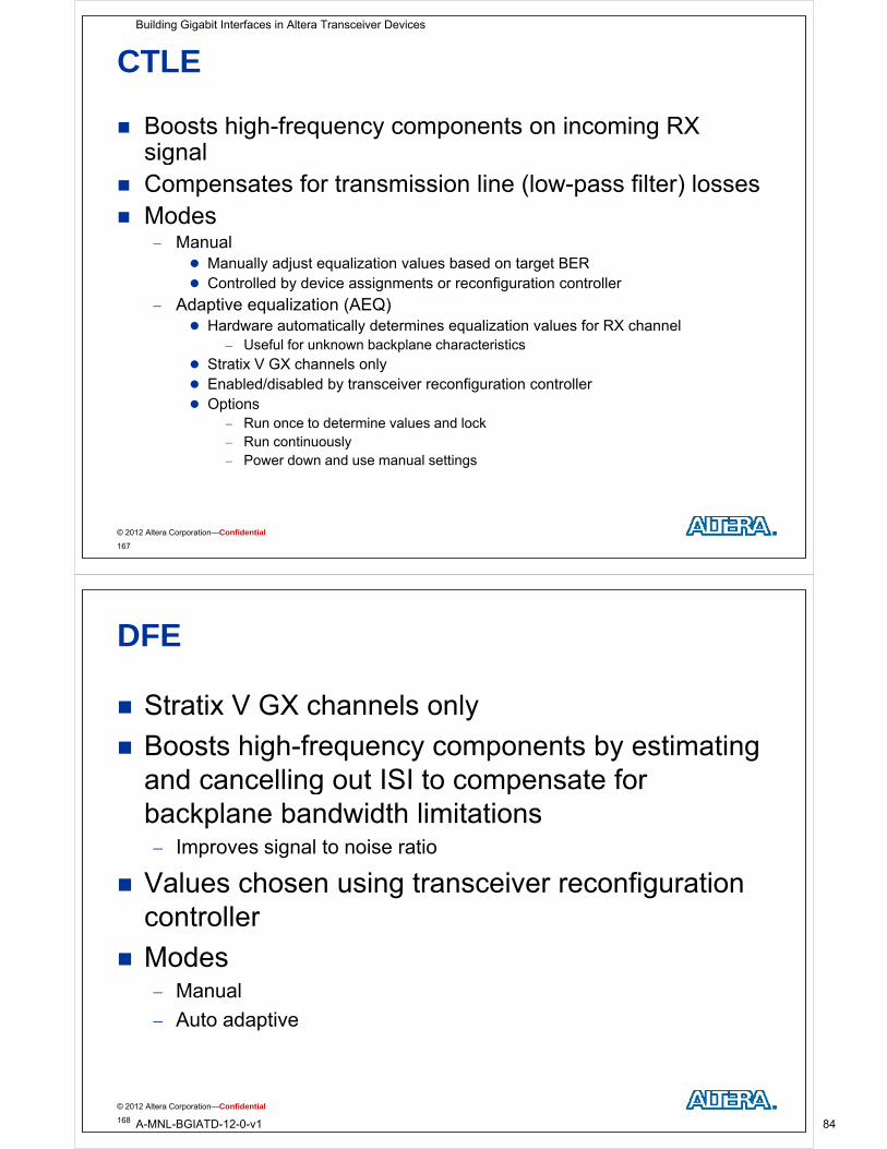
CTLE
Boosts high-frequency components on incoming RX signalsignal
Compensates for transmission line (low-pass filter) losses Modes Modes
Manual Manually adjust equalization values based on target BER Controlled by device assignments or reconfiguration controller Controlled by device assignments or reconfiguration controller
Adaptive equalization (AEQ) Hardware automatically determines equalization values for RX channel
Useful for unknown backplane characteristics
Stratix V GX channels only Enabled/disabled by transceiver reconfiguration controller Options
Run once to determine values and lock Run once to determine values and lock Run continuously Power down and use manual settings
© 2012 Altera Corporation—Confidential
167
DFE
Stratix V GX channels only
Boosts high-frequency components by estimating and cancelling out ISI to compensate for g pbackplane bandwidth limitations Improves signal to noise ratio
Values chosen using transceiver reconfiguration controller
Modes ManualManual
Auto adaptive
© 2012 Altera Corporation—Confidential
168
Building Gigabit Interfaces in Altera Transceiver Devices
A-MNL-BGIATD-12-0-v1 84
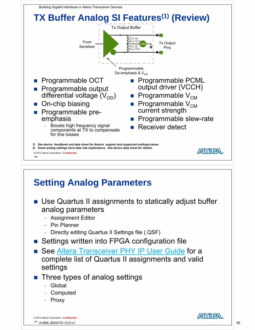
TX Buffer Analog SI Features(1) (Review)
42.5, 50,60 or 75 Ω
Tx Output+CM
Tx Output Buffer
From Tx Output Pins
+CM-Serializer 42.5, 50,
60 or 75 Ω
Programmable OCT Programmable PCML
Programmable De-emphasis & VOD
Programmable OCT Programmable output
differential voltage (VOD)O hi bi i
Programmable PCMLoutput driver (VCCH)
Programmable VCM
P bl V On-chip biasing Programmable pre-
emphasis
Programmable VCMcurrent strength
Programmable slew-ratep Boosts high frequency signal
components at TX to compensate for line losses
g Receiver detect
© 2012 Altera Corporation—Confidential
169
1) See device handbook and data sheet for feature support and supported settings/values2) Some analog settings have data rate implications. See device data sheet for details.
Setting Analog Parameters
Use Quartus II assignments to statically adjust buffer analog parametersanalog parameters Assignment Editor Pin Planner Directly editing Quartus II Settings file (.QSF)
Settings written into FPGA configuration file See Altera Transceiver PHY IP User Guide for a
complete list of Quartus II assignments and valid settingssettings
Three types of analog settings GlobalGlobal Computed Proxy
© 2012 Altera Corporation—Confidential
170
Building Gigabit Interfaces in Altera Transceiver Devices
A-MNL-BGIATD-12-0-v1 85
Analog Settings
Global settingsD f l l i d d f h i Default values independent of other settings
Designer may choose to optimize based on board conditions Examplesp
PLL_BANDWIDTH_PRESET: Auto, Low, Medium, High XCVR_RX _DC_GAIN: 0 – 4 XCVR RX LINEAR EQUALIZER CONTROL: 1 – 16 XCVR_RX_LINEAR_EQUALIZER_CONTROL: 1 16
Computed settings Default values calculated from other settingsg Designer may choose to optimize based on board conditions Examples
XCVR TX VOD: 0 63 XCVR_TX_VOD: 0 – 63 XCVR_RX_COMMON_MODE_VOLTAGE: Various values
© 2012 Altera Corporation—Confidential
171
Analog Settings (cont.)
Placeholder settings Default values assigned
Designer expected to replace defaults with values based on board/system specificationboard/system specification
Examples XCVR_IO_PIN_TERMINATION: 85_OHMS, 100_OHMS,
120_OHMS, 150_OHMS, EXTERNAL_RESISTOR
XCVR_VCCA_VOLTAGE: 2_5V, 3_0V Valid settings are data rate dependent
Fixed for some devices
XCVR_TX_SLEW_RATE_CTRL: 1 – 5
© 2012 Altera Corporation—Confidential
172
Building Gigabit Interfaces in Altera Transceiver Devices
A-MNL-BGIATD-12-0-v1 86
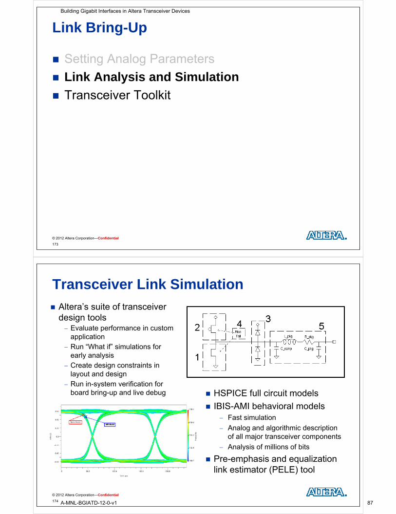
Link Bring-Up
Setting Analog Parameters
Link Analysis and Simulation
Transceiver Toolkit Transceiver Toolkit
© 2012 Altera Corporation—Confidential
173
Transceiver Link Simulation
Altera’s suite of transceiver design tools Evaluate performance in custom
application Run “What if” simulations for
early analysisearly analysis Create design constraints in
layout and design Run in-system verification forRun in system verification for
board bring-up and live debug HSPICE full circuit models
IBIS-AMI behavioral modelsF t i l ti Fast simulation
Analog and algorithmic description of all major transceiver components
Analysis of millions of bits Analysis of millions of bits
Pre-emphasis and equalization link estimator (PELE) tool
© 2012 Altera Corporation—Confidential
174
Building Gigabit Interfaces in Altera Transceiver Devices
A-MNL-BGIATD-12-0-v1 87
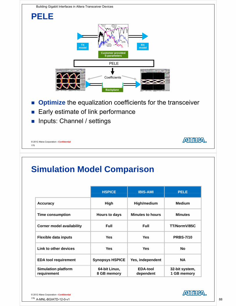
PELE
TXmodel
RXmodel
Customer provided S-parameters
PELE
C ffi i t
Backplane
Coefficients
Optimize the equalization coefficients for the transceiver
Early estimate of link performance Early estimate of link performance
Inputs: Channel / settings
© 2012 Altera Corporation—Confidential
175
Simulation Model Comparison
HSPICE IBIS-AMI PELEHSPICE IBIS AMI PELE
Accuracy High High/medium Medium
Time consumption Hours to days Minutes to hours Minutes
Corner model availability Full Full TT/NormV/85C
Flexible data inputs Yes Yes PRBS-7/10
Li k t th d i Y Y NLink to other devices Yes Yes No
EDA tool requirement Synopsys HSPICE Yes, independent NA
Simulation platform requirement
64-bit Linux, 8 GB memory
EDA-tool dependent
32-bit system, 1 GB memory
© 2012 Altera Corporation—Confidential
176
Building Gigabit Interfaces in Altera Transceiver Devices
A-MNL-BGIATD-12-0-v1 88
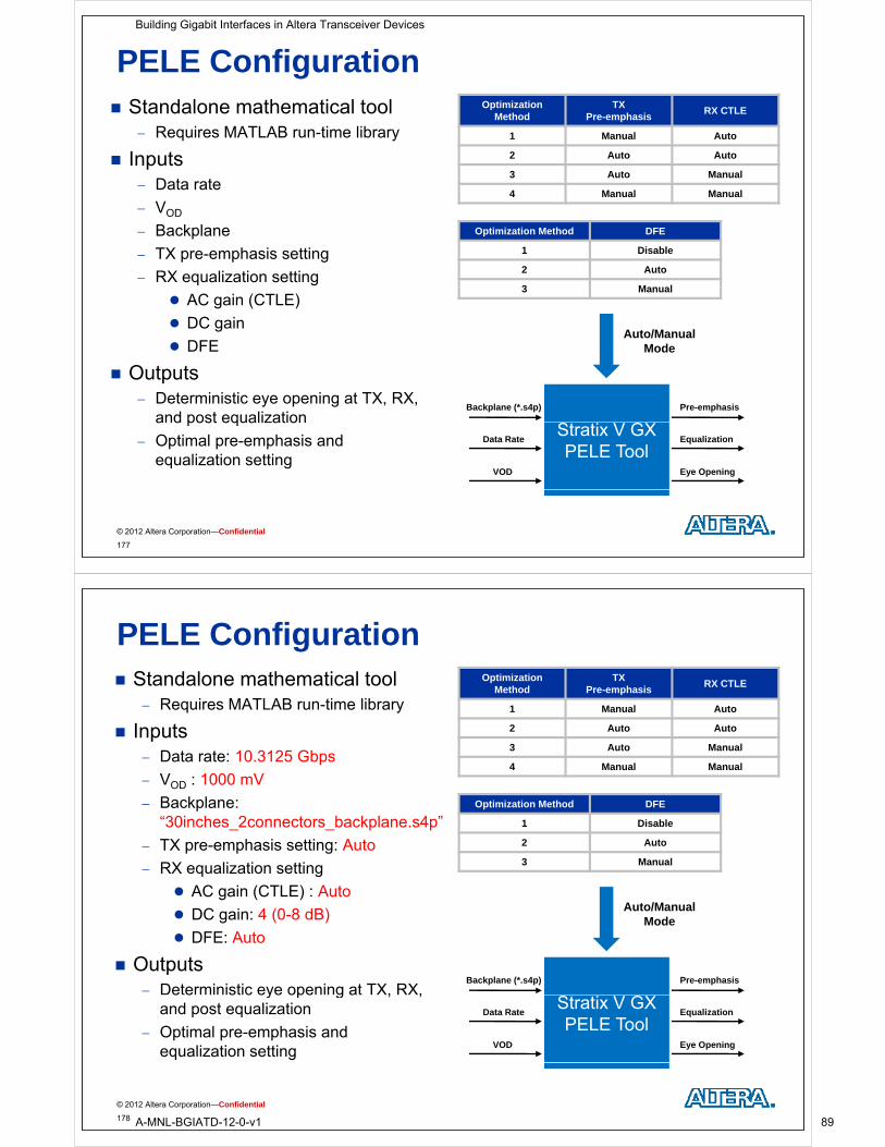
PELE ConfigurationOptimization
MethodTX
Pre-emphasisRX CTLE
1 Manual Auto
Standalone mathematical tool Requires MATLAB run-time library
2 Auto Auto
3 Auto Manual
4 Manual Manual
Inputs Data rate
VOD
Backplane
TX pre-emphasis setting
RX equalization setting
Optimization Method DFE
1 Disable
2 Auto
3 M l AC gain (CTLE)
DC gain
DFE
3 Manual
Auto/ManualMode
Outputs Deterministic eye opening at TX, RX,
and post equalizationBackplane (*.s4p) Pre-emphasis
and post equalization
Optimal pre-emphasis and equalization setting
Stratix V GXPELE Tool
Data Rate
VOD
Equalization
Eye Opening
© 2012 Altera Corporation—Confidential
177
PELE ConfigurationOptimization
MethodTX
Pre-emphasisRX CTLE
1 Manual Auto
Standalone mathematical tool Requires MATLAB run-time library
I t 2 Auto Auto
3 Auto Manual
4 Manual Manual
Inputs Data rate: 10.3125 Gbps
VOD : 1000 mV
Backplane: “30inches_2connectors_backplane.s4p”
TX pre-emphasis setting: Auto
Optimization Method DFE
1 Disable
2 Auto
3 M l RX equalization setting
AC gain (CTLE) : Auto
DC gain: 4 (0-8 dB)
3 Manual
Auto/ManualMode
DFE: Auto
Outputs Deterministic eye opening at TX, RX,
Backplane (*.s4p) Pre-emphasise e s c eye ope g a , ,
and post equalization
Optimal pre-emphasis and equalization setting
Stratix V GXPELE Tool
Data Rate
VOD
Equalization
Eye Opening
© 2012 Altera Corporation—Confidential
178
Building Gigabit Interfaces in Altera Transceiver Devices
A-MNL-BGIATD-12-0-v1 89
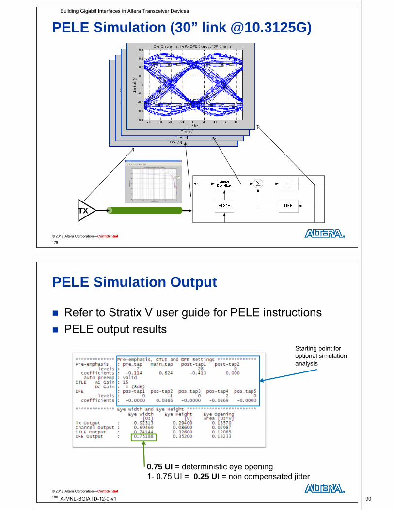
PELE Simulation (30” link @10.3125G)
TX
© 2012 Altera Corporation—Confidential
179
PELE Simulation Output
Refer to Stratix V user guide for PELE instructions
PELE output results
Starting point for optional simulation analysis
0.75 UI = deterministic eye opening
© 2012 Altera Corporation—Confidential
180
1- 0.75 UI = 0.25 UI = non compensated jitter
Building Gigabit Interfaces in Altera Transceiver Devices
A-MNL-BGIATD-12-0-v1 90
Obtaining Link Analysis and Simulation Files Contact Altera representative or mySupport for Contact Altera representative or mySupport for
files
© 2012 Altera Corporation—Confidential
181
Link Bring-Up
Setting Analog Parameters
Link Analysis and Simulation
Transceiver Toolkit Transceiver Toolkit
© 2012 Altera Corporation—Confidential
182
Building Gigabit Interfaces in Altera Transceiver Devices
A-MNL-BGIATD-12-0-v1 91
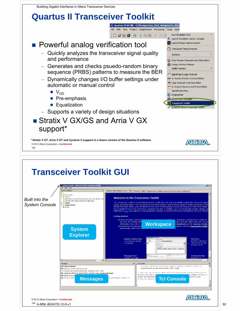
Quartus II Transceiver Toolkit
Powerful analog verification tool Quickly analyzes the transceiver signal quality
and performanceand performance Generates and checks psuedo-random binary
sequence (PRBS) patterns to measure the BERD i ll h I/O b ff tti d Dynamically changes I/O buffer settings under automatic or manual control VOD
Pre-emphasis Equalization
Supports a variety of design situationspp y g
Stratix V GX/GS and Arria V GX support*
© 2012 Altera Corporation—Confidential
pp
183
* Stratix V GT, Arria V GT and Cyclone V support in a future version of the Quartus II software.
Transceiver Toolkit GUI
Built into the System Console
WorkspaceSystem Explorer
Messages Tcl Console
© 2012 Altera Corporation—Confidential
184
Building Gigabit Interfaces in Altera Transceiver Devices
A-MNL-BGIATD-12-0-v1 92
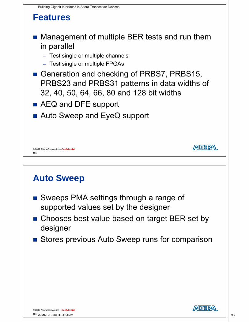
Features
Management of multiple BER tests and run them in parallel Test single or multiple channels
Test single or multiple FPGAs
Generation and checking of PRBS7, PRBS15, PRBS23 d PRBS31 tt i d t idth fPRBS23 and PRBS31 patterns in data widths of 32, 40, 50, 64, 66, 80 and 128 bit widths
AEQ and DFE support
Auto Sweep and EyeQ supportp y Q pp
© 2012 Altera Corporation—Confidential
185
Auto Sweep
Sweeps PMA settings through a range of supported values set by the designer
Chooses best value based on target BER set by g ydesigner
Stores previous Auto Sweep runs for comparison Stores previous Auto Sweep runs for comparison
© 2012 Altera Corporation—Confidential
186
Building Gigabit Interfaces in Altera Transceiver Devices
A-MNL-BGIATD-12-0-v1 93

EyeQ
Sweeps receiver sampling point across an entire input unit interval (UI)unit interval (UI) Circuitry generates 64 horizontal and vertical sampling positions within 1
UI of received input
Can also sweep horizontal only (bathtub curve)
Monitors BER of input signal to determine eye width and h i htheight
Available in Stratix V transceiver devices
© 2012 Altera Corporation—Confidential
187
Using EyeQ
EyeQ diagram is based on BER measurements Not the same as actual “eye” scope measurement
Uses Compare PMA settings for the same channel
Choose the best combination of PMA settings for a particular channelchannel
Should not compare results against other channels or eye diagrams from other vendorschannels or eye diagrams from other vendors
© 2012 Altera Corporation—Confidential
188
Building Gigabit Interfaces in Altera Transceiver Devices
A-MNL-BGIATD-12-0-v1 94
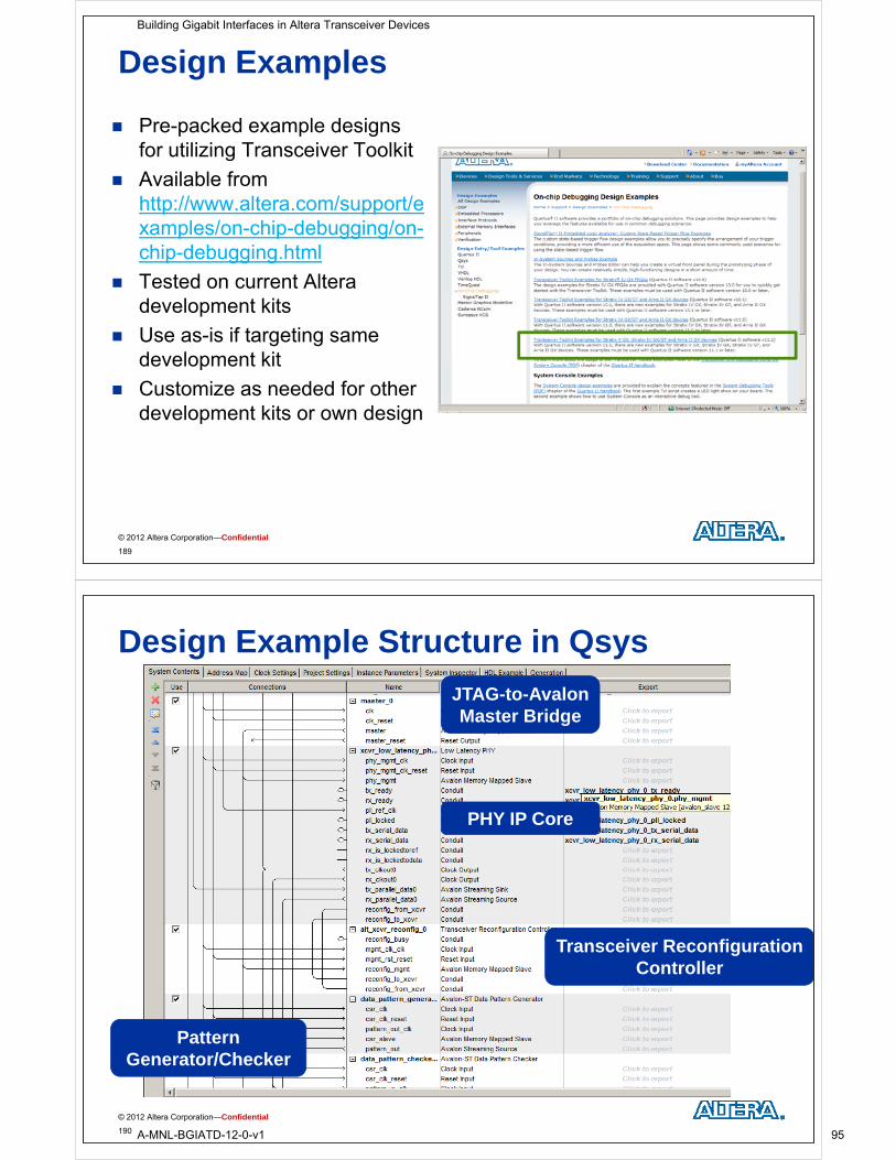
Design Examples
Pre-packed example designs for utilizing Transceiver Toolkitfor utilizing Transceiver Toolkit
Available from http://www.altera.com/support/e
l / hi d b i /xamples/on-chip-debugging/on-chip-debugging.html
Tested on current Alteradevelopment kits
Use as-is if targeting same development kitdevelopment kit
Customize as needed for other development kits or own design
© 2012 Altera Corporation—Confidential
189
Design Example Structure in Qsys
JTAG-to-Avalon Master Bridge
PHY IP Core
Transceiver Reconfiguration Controller
Pattern Generator/Checker
© 2012 Altera Corporation—Confidential
190
Building Gigabit Interfaces in Altera Transceiver Devices
A-MNL-BGIATD-12-0-v1 95
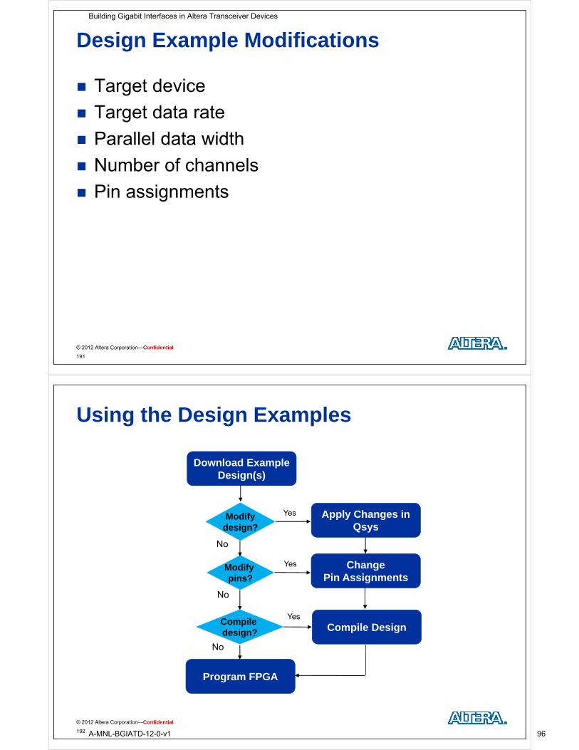
Design Example Modifications
Target device
Target data rate
Parallel data width Parallel data width
Number of channels
Pi i t Pin assignments
© 2012 Altera Corporation—Confidential
191
Using the Design Examples
Download ExampleDesign(s)Design(s)
Modify Apply Changes inYesModifydesign?
Ch
pp y C a gesQsys
Y
No
Change Pin Assignments
No
Modify pins?
Yes
Compile DesignCompile design?
No
Yes
Program FPGA
© 2012 Altera Corporation—Confidential
192
Building Gigabit Interfaces in Altera Transceiver Devices
A-MNL-BGIATD-12-0-v1 96
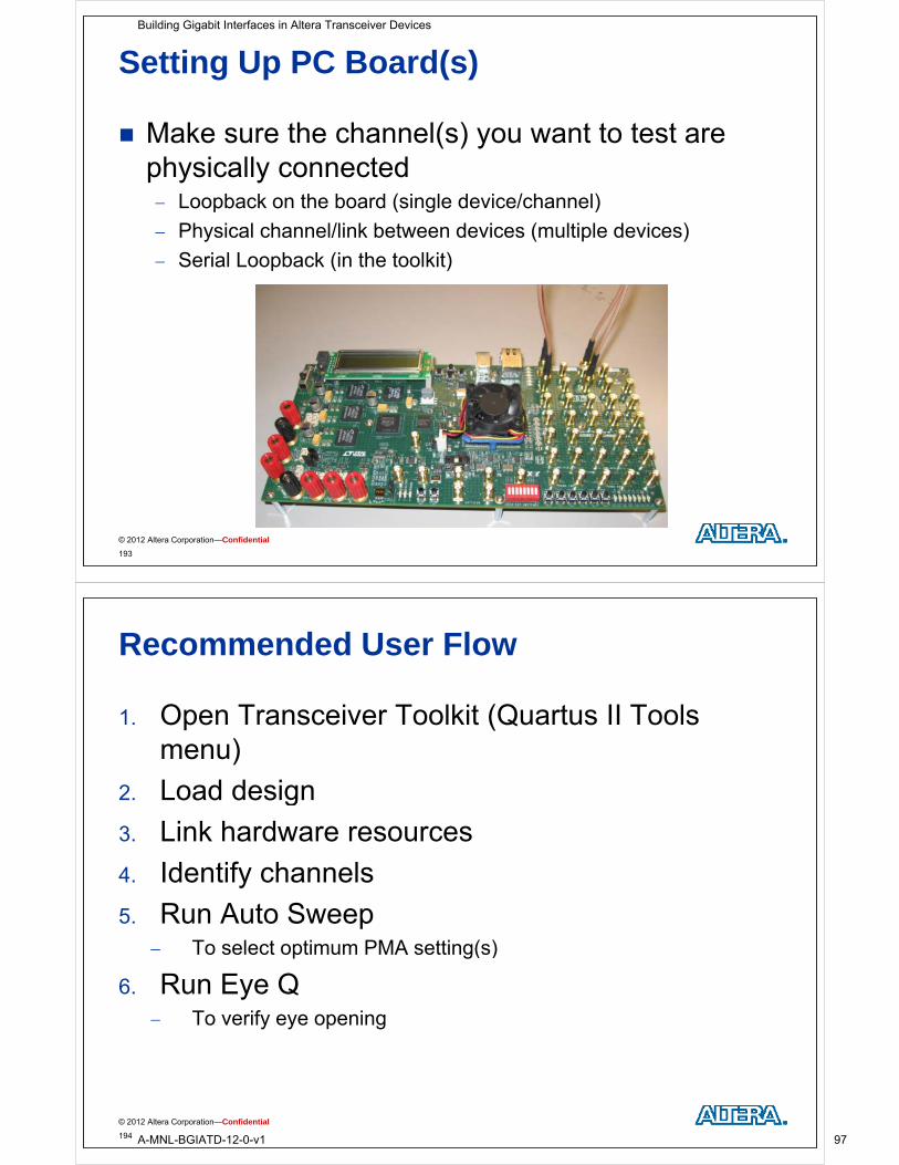
Setting Up PC Board(s)
Make sure the channel(s) you want to test are physically connected Loopback on the board (single device/channel)
Physical channel/link between devices (multiple devices)
Serial Loopback (in the toolkit)
© 2012 Altera Corporation—Confidential
193
Recommended User Flow
1. Open Transceiver Toolkit (Quartus II Tools menu)
2. Load designg
3. Link hardware resources
4 Identify channels4. Identify channels
5. Run Auto SweepT l t ti PMA tti ( ) To select optimum PMA setting(s)
6. Run Eye QT if i To verify eye opening
© 2012 Altera Corporation—Confidential
194
Building Gigabit Interfaces in Altera Transceiver Devices
A-MNL-BGIATD-12-0-v1 97
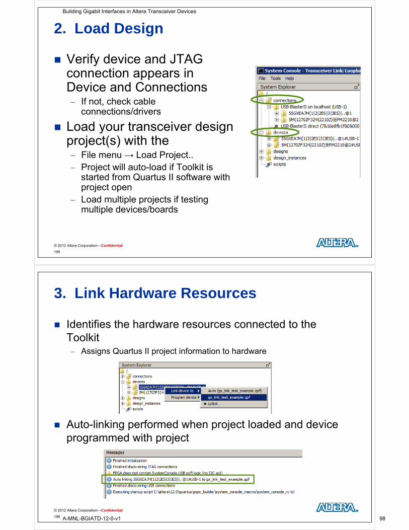
2. Load Design
Verify device and JTAG ti iconnection appears in
Device and Connections If not check cable If not, check cable connections/drivers
Load your transceiver design y gproject(s) with the File menu → Load Project..
P j t ill t l d if T lkit i Project will auto-load if Toolkit is started from Quartus II software with project open
Load multiple projects if testing multiple devices/boards
© 2012 Altera Corporation—Confidential
195
3. Link Hardware Resources
Identifies the hardware resources connected to the T lkitToolkit Assigns Quartus II project information to hardware
Auto-linking performed when project loaded and device g p p jprogrammed with project
© 2012 Altera Corporation—Confidential
196
Building Gigabit Interfaces in Altera Transceiver Devices
A-MNL-BGIATD-12-0-v1 98

4. Identify Channels
Design RX and TX channels will automatically display in Transmitter Channels and Receiver Ch l t bChannels tabs
Create link to indicate the TX→RX channel connectionsconnections Auto-links created between RX/TX paths in same channels Create new links to connect TX and RX on different transceiver
channels or different deviceschannels or different devices Change link alias to create a more “user-friendly” link name
© 2012 Altera Corporation—Confidential
197
Running Tests
Highlight link
Click buttons for Auto Sweep or
EyeQ tests
© 2012 Altera Corporation—Confidential
198
Building Gigabit Interfaces in Altera Transceiver Devices
A-MNL-BGIATD-12-0-v1 99
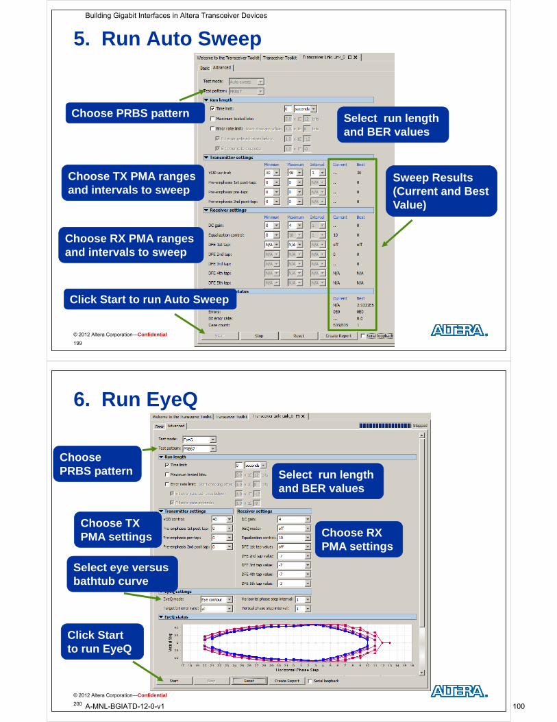
5. Run Auto Sweep
Choose PRBS pattern Select run length and BER values
Choose TX PMA ranges Sweep Resultsgand intervals to sweep
Sweep Results (Current and Best Value)
Choose RX PMA ranges and intervals to sweep
Click Start to run Auto Sweep
© 2012 Altera Corporation—Confidential
199
6. Run EyeQ
ChooseChoose PRBS pattern Select run length
and BER values
Choose TXPMA settings Choose RX g
PMA settings
Select eye versus bathtub curvebathtub curve
Click Start to run EyeQ
© 2012 Altera Corporation—Confidential
200
Building Gigabit Interfaces in Altera Transceiver Devices
A-MNL-BGIATD-12-0-v1 100
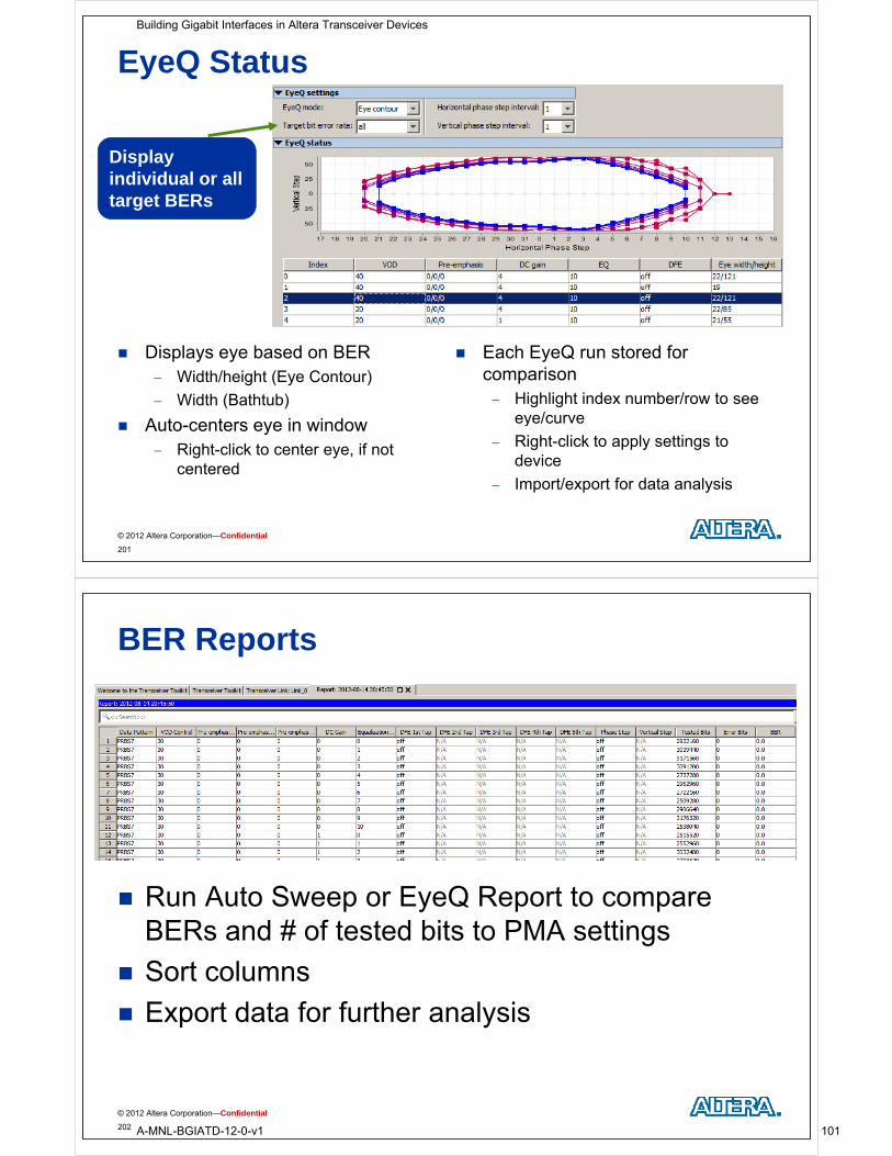
EyeQ Status
Di lDisplayindividual or all target BERs
Displays eye based on BER Each EyeQ run stored for Displays eye based on BER Width/height (Eye Contour)
Width (Bathtub)
Auto centers eye in window
Each EyeQ run stored for comparison Highlight index number/row to see
eye/curve Auto-centers eye in window
Right-click to center eye, if not centered
y
Right-click to apply settings to device
Import/export for data analysis
© 2012 Altera Corporation—Confidential
201
BER Reports
Run Auto Sweep or EyeQ Report to compare BERs and # of tested bits to PMA settingsBERs and # of tested bits to PMA settings
Sort columns
E t d t f f th l i Export data for further analysis
© 2012 Altera Corporation—Confidential
202
Building Gigabit Interfaces in Altera Transceiver Devices
A-MNL-BGIATD-12-0-v1 101
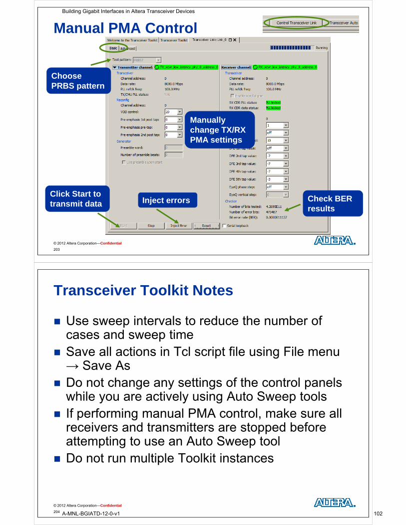
Manual PMA Control
Choose PRBS pattern
Manually change TX/RXchange TX/RX PMA settings
Click Start toClick Start to transmit data
Check BER results
Inject errors
© 2012 Altera Corporation—Confidential
203
Transceiver Toolkit Notes
Use sweep intervals to reduce the number of d ticases and sweep time
Save all actions in Tcl script file using File menu S A→ Save As
Do not change any settings of the control panels hil ti l i A t S t lwhile you are actively using Auto Sweep tools
If performing manual PMA control, make sure all i d t itt t d b freceivers and transmitters are stopped before
attempting to use an Auto Sweep toolD t lti l T lkit i t Do not run multiple Toolkit instances
© 2012 Altera Corporation—Confidential
204
Building Gigabit Interfaces in Altera Transceiver Devices
A-MNL-BGIATD-12-0-v1 102
References
See the Board Design Resource Center for Altera recommendations on board development
Transceiver Link Debugging Using the System gg g g yConsole chapter of the Quartus II Handbook
© 2012 Altera Corporation—Confidential
205
Test Your Knowledge
1. What are the 2 types of equalization supported in StratixV GX transceivers?A. CTLE and DFEV GX transceivers?
2. What are the 3 link simulation strategies supported by Altera?
A. PELE, IBIS-AMI and HSPICE
3. What are the two steps in the recommended Toolkit flow that help choose optimum PMA settings and verify them?
A. Running Auto Sweep and EyeQ
© 2012 Altera Corporation—Confidential
206
Building Gigabit Interfaces in Altera Transceiver Devices
A-MNL-BGIATD-12-0-v1 103

Please go to Exercise 4g
© 2012 Altera Corporation—Confidential
207
Building Gigabit Interfaces inBuilding Gigabit Interfaces in Altera Transceiver DevicesT i R fi tiTransceiver Reconfiguration
© 2012 Altera Corporation—Confidential
Building Gigabit Interfaces in Altera Transceiver Devices
A-MNL-BGIATD-12-0-v1 104
Section Objectives
Indicate the reconfigurable options of 28-nm embedded transceivers
Incorporate the dynamic reconfiguration p y gcontroller into your transceiver design
Utilize the dynamic reconfiguration controller and Utilize the dynamic reconfiguration controller and hardware to change transceiver parameters without reconfiguring the FPGAwithout reconfiguring the FPGA
© 2012 Altera Corporation—Confidential
209
Section Agenda
Introduction
Transceiver Reconfiguration Controller
Example Reconfigurations Example Reconfigurations Calibration
PMA Reconfiguration
Introduction to TX PLL Switching
© 2012 Altera Corporation—Confidential
210
Building Gigabit Interfaces in Altera Transceiver Devices
A-MNL-BGIATD-12-0-v1 105
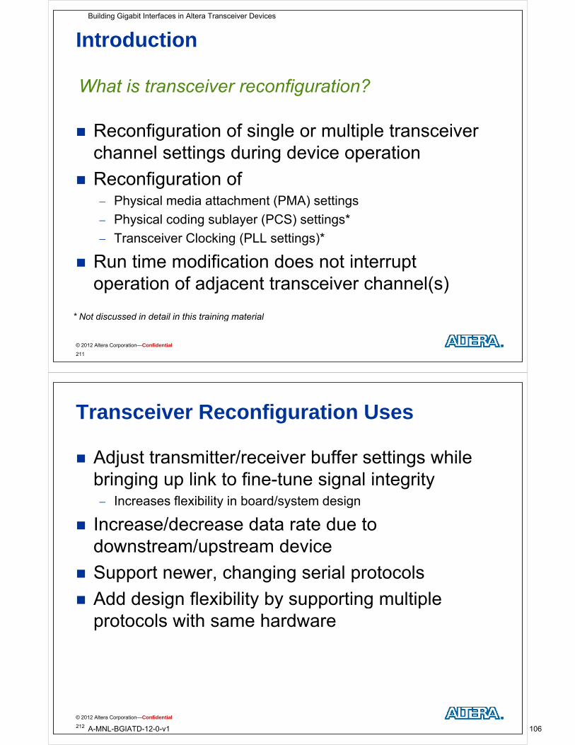
Introduction
What is transceiver reconfiguration?
Reconfiguration of single or multiple transceiver channel settings during device operation
Reconfiguration ofg Physical media attachment (PMA) settings
Physical coding sublayer (PCS) settings*
Transceiver Clocking (PLL settings)*
Run time modification does not interrupt operation of adjacent transceiver channel(s)
* Not discussed in detail in this training material
© 2012 Altera Corporation—Confidential
211
Not discussed in detail in this training material
Transceiver Reconfiguration Uses
Adjust transmitter/receiver buffer settings while bringing up link to fine-tune signal integrity Increases flexibility in board/system design
Increase/decrease data rate due to downstream/upstream device
Support newer, changing serial protocols
Add design flexibility by supporting multiple Add design flexibility by supporting multiple protocols with same hardware
© 2012 Altera Corporation—Confidential
212
Building Gigabit Interfaces in Altera Transceiver Devices
A-MNL-BGIATD-12-0-v1 106

Why Should I Care about Reconfiguration?
Certain transceiver resources require calibration upon power up RX channel buffers ATX PLLsATX PLLs
Calibration performed automatically by reconfiguration controllerreconfiguration controller
Quartus II software requires all transceiver designs to have a reconfiguration controllerdesigns to have a reconfiguration controller connected Even if no plan to change transceiver features dynamically Connect controller and never operate
© 2012 Altera Corporation—Confidential
213
Reconfiguration and Device Support
Reconfiguration FeatureDevice Family
Cyclone V Arria V Stratix V
Calibration
AnalogPMA Reconfiguration
AnalogEyeQ, AEQ, DFE*
LoopbackPre-CDR reverse serial
Post CDR reverse serial Post-CDR reverse serial
PLLReconfiguration
Ref Clk Switching * *
TX PLL Reconfiguration *
Channel
RX CDR Reconfiguration *
PCS Reconfiguration * Channel Reconfiguration TX PLL Switching *
TX Channel Divider *
FPGA/Transceiver Data Width *
© 2012 Altera Corporation—Confidential
214
* Support enabled in a future version of the Quartus II software.
Building Gigabit Interfaces in Altera Transceiver Devices
A-MNL-BGIATD-12-0-v1 107
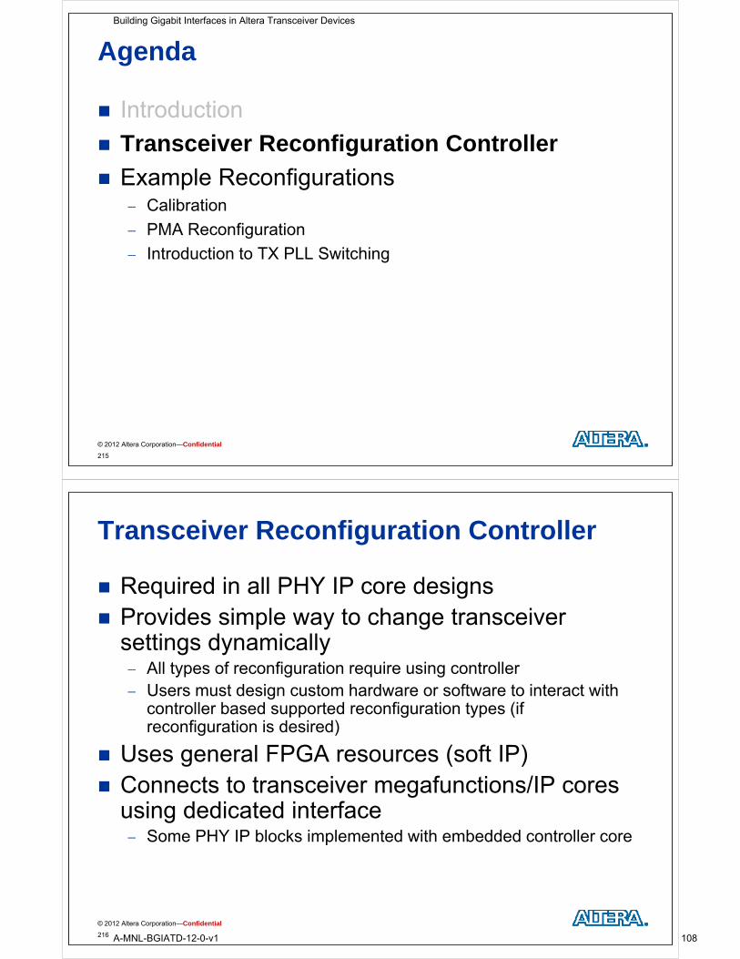
Agenda
Introduction
Transceiver Reconfiguration Controller
Example Reconfigurations Example Reconfigurations Calibration
PMA Reconfiguration
Introduction to TX PLL Switching
© 2012 Altera Corporation—Confidential
215
Transceiver Reconfiguration Controller
Required in all PHY IP core designs Provides simple way to change transceiver
settings dynamicallyAll t f fi ti i i t ll All types of reconfiguration require using controller
Users must design custom hardware or software to interact with controller based supported reconfiguration types (if reconfiguration is desired)
Uses general FPGA resources (soft IP) Connects to transceiver megafunctions/IP cores
using dedicated interfaceS PHY IP bl k i l t d ith b dd d t ll Some PHY IP blocks implemented with embedded controller core
© 2012 Altera Corporation—Confidential
216
Building Gigabit Interfaces in Altera Transceiver Devices
A-MNL-BGIATD-12-0-v1 108
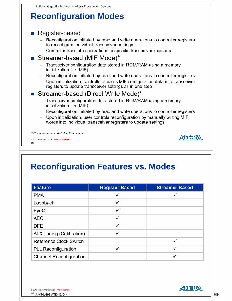
Reconfiguration Modes
Register-basedReconfiguration initiated by read and write operations to controller registers Reconfiguration initiated by read and write operations to controller registers to reconfigure individual transceiver settings
Controller translates operations to specific transceiver registers
Streamer based (MIF Mode)* Streamer-based (MIF Mode) Transceiver configuration data stored in ROM/RAM using a memory
initialization file (MIF)Reconfiguration initiated by read and write operations to controller registers Reconfiguration initiated by read and write operations to controller registers
Upon initialization, controller steams MIF configuration data into transceiver registers to update transceiver settings all in one step
Streamer based (Direct Write Mode)* Streamer-based (Direct Write Mode)* Transceiver configuration data stored in ROM/RAM using a memory
initialization file (MIF)Reconfiguration initiated by read and write operations to controller registers Reconfiguration initiated by read and write operations to controller registers
Upon initialization, user controls reconfiguration by manually writing MIF words into individual transceiver registers to update settings
© 2012 Altera Corporation—Confidential
217
* Not discussed in detail in this course.
Reconfiguration Features vs. Modes
Feature Register-Based Streamer-Basedg
PMA
Loopback
EyeQ
AEQ
DFE DFE
ATX Tuning (Calibration)
Reference Clock Switch
PLL Reconfiguration
Channel Reconfiguration
© 2012 Altera Corporation—Confidential
218
Building Gigabit Interfaces in Altera Transceiver Devices
A-MNL-BGIATD-12-0-v1 109
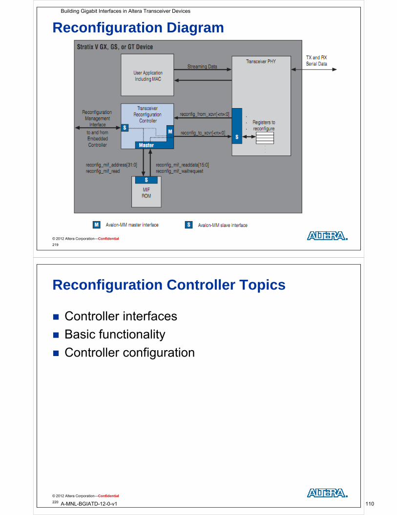
Reconfiguration Diagram
© 2012 Altera Corporation—Confidential
219
Reconfiguration Controller Topics
Controller interfaces
Basic functionality
Controller configuration Controller configuration
© 2012 Altera Corporation—Confidential
220
Building Gigabit Interfaces in Altera Transceiver Devices
A-MNL-BGIATD-12-0-v1 110
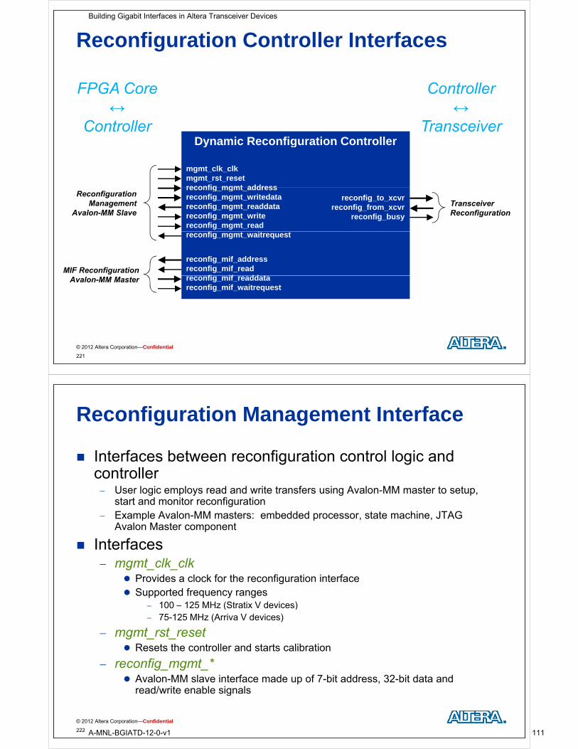
Reconfiguration Controller Interfaces
FPGA Core Controller
Dynamic Reconfiguration Controller
↔ Controller
↔ Transceiver
Dynamic Reconfiguration Controller
mgmt_clk_clkmgmt_rst_resetreconfig mgmt addressreconfig_mgmt_addressreconfig_mgmt_writedatareconfig_mgmt_readdatareconfig_mgmt_writereconfig_mgmt_read
reconfig_to_xcvrreconfig_from_xcvr
reconfig_busy
Reconfiguration Management
Avalon-MM SlaveTransceiver Reconfiguration
reconfig_mgmt_waitrequest
reconfig_mif_addressreconfig_mif_read
fi if dd tMIF Reconfiguration
reconfig_mif_readdatareconfig_mif_waitrequest
Avalon-MM Master
© 2012 Altera Corporation—Confidential
221
Reconfiguration Management Interface
Interfaces between reconfiguration control logic and controllercontroller User logic employs read and write transfers using Avalon-MM master to setup,
start and monitor reconfiguration Example Avalon-MM masters: embedded processor state machine JTAGExample Avalon MM masters: embedded processor, state machine, JTAG
Avalon Master component
Interfacesmgmt clk clk mgmt_clk_clk Provides a clock for the reconfiguration interface Supported frequency ranges
100 – 125 MHz (Stratix V devices) 100 – 125 MHz (Stratix V devices) 75-125 MHz (Arriva V devices)
mgmt_rst_reset Resets the controller and starts calibration Resets the controller and starts calibration
reconfig_mgmt_* Avalon-MM slave interface made up of 7-bit address, 32-bit data and
read/write enable signals
© 2012 Altera Corporation—Confidential
g
222
Building Gigabit Interfaces in Altera Transceiver Devices
A-MNL-BGIATD-12-0-v1 111
MIF Reconfiguration Interface
Avalon-MM master interface between controller and MIF storage locationstorage location Controller accesses MIF data based on requests received through its slave
interface
Interface Interface reconfig_mif_*
Master interface made up of 32-bit address, 16-bit data, read enable and it t i lwaitrequest signals
© 2012 Altera Corporation—Confidential
223
Transceiver Reconfiguration Interface
Dedicated interface between controller and transceiver IP core Controller reads values from and writes values to transceiver registers based onController reads values from and writes values to transceiver registers based on
requests received through its slave interface
Each transceiver instance has 1 reconfiguration interface on per each transceiver channel and each TX PLLper each transceiver channel and each TX PLL
Signals reconfig_to_xcvr[(n*70)-1..0]
O t t i l f t ll t t i IP i t ( ) Output signal from controller to transceiver IP core instance(s) n = number of reconfiguration interfaces
reconfig_from_xcvr[(n*46)-1..0] Input signal to controller from transceiver IP core instance(s) Input signal to controller from transceiver IP core instance(s) n = number of reconfiguration interfaces
reconfig_busy Output signal that indicates when a reconfiguration operation is in progress Output signal that indicates when a reconfiguration operation is in progress Similar to the busy bits (bit 8) in the control and status registers
© 2012 Altera Corporation—Confidential
224
Building Gigabit Interfaces in Altera Transceiver Devices
A-MNL-BGIATD-12-0-v1 112
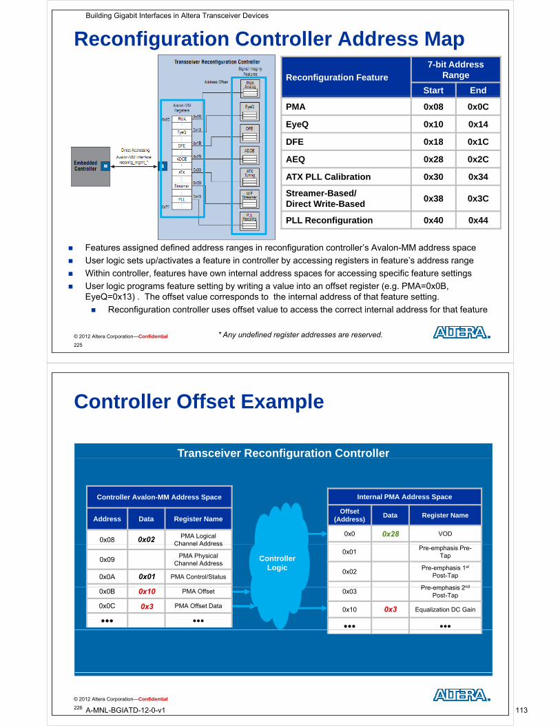
Reconfiguration Controller Address Map
Reconfiguration Feature
7-bit Address Range
Start End
PMA 0x08 0x0C
EyeQ 0x10 0x14
DFE 0 18 0 1CDFE 0x18 0x1C
AEQ 0x28 0x2C
ATX PLL Calibration 0x30 0x34
Streamer-Based/Direct Write-Based
0x38 0x3C
PLL Reconfiguration 0x40 0x44g
Features assigned defined address ranges in reconfiguration controller’s Avalon-MM address space
User logic sets up/activates a feature in controller by accessing registers in feature’s address range
Within controller, features have own internal address spaces for accessing specific feature settings
User logic programs feature setting by writing a value into an offset register (e.g. PMA=0x0B, EyeQ=0x13) . The offset value corresponds to the internal address of that feature setting.
Reconfiguration controller uses offset value to access the correct internal address for that feature
© 2012 Altera Corporation—Confidential
225
* Any undefined register addresses are reserved.
Reconfiguration controller uses offset value to access the correct internal address for that feature
Controller Offset Example
Transceiver Reconfiguration Controllerg
Internal PMA Address SpaceController Avalon-MM Address Space
Offset (Address)
Data Register Name
0x0 VOD0x28
Address Data Register Name
0x08PMA Logical
Channel Address0x02
Controller Logic
0x01Pre-emphasis Pre-
Tap
0x02Pre-emphasis 1st
Post-Tap
Pre emphasis 2nd
Channel Address
0x09PMA Physical
Channel Address
0x0A PMA Control/Status0x010x01
0x03Pre-emphasis 2nd
Post-Tap
0x10 Equalization DC Gain
0x3
0x0B PMA Offset
0x0C PMA Offset Data
0x0
0x28
0x10
0x3
© 2012 Altera Corporation—Confidential
226
Building Gigabit Interfaces in Altera Transceiver Devices
A-MNL-BGIATD-12-0-v1 113
Logical Channel Numbers
Reference numbers used to represent actual physical transceiver channels and TX PLLsphysical transceiver channels and TX PLLs
Used during reconfiguration to target specific channels or PLLschannels or PLLs Controller translates read/write operations to logical channel
numbers to their corresponding physical channels
Assigned to physical transceivers automatically based on
Number of channels and TX PLLs in transceiver IP cores Number of channels and TX PLLs in transceiver IP cores Order in which the reconfiguration interfaces are physically
connected to controllerVi th i t lt i th T i R fi ti View the assignment results in the Transceiver Reconfiguration Report (Compilation Report → Fitter → GXB Reports)
© 2012 Altera Corporation—Confidential
227
Basic Register-Based Write Operation
1. Read feature control and status register to determine busy bit is 0y
2. Write target logical channel number to feature’s logical_channel_address register
3. Write the internal address (offset) value to feature’s offset register
4. Write the target value for the feature setting into the feature data registerW it f t ’ t l d t t i t it bit5. Write feature’s control and status register write bit with 1
6 Transceiver is programmed when busy bit is 06. Transceiver is programmed when busy bit is 0 again
© 2012 Altera Corporation—Confidential
228
Building Gigabit Interfaces in Altera Transceiver Devices
A-MNL-BGIATD-12-0-v1 114
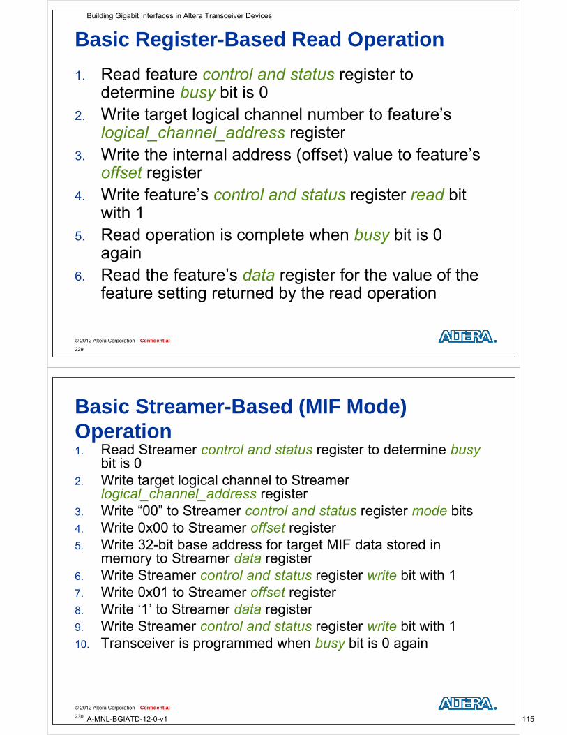
Basic Register-Based Read Operation
1. Read feature control and status register to determine busy bit is 0determine busy bit is 0
2. Write target logical channel number to feature’s logical_channel_address registerg _ _ g
3. Write the internal address (offset) value to feature’s offset register
4. Write feature’s control and status register read bit with 1
5. Read operation is complete when busy bit is 0 againR d th f t ’ d t i t f th l f th6. Read the feature’s data register for the value of the feature setting returned by the read operation
© 2012 Altera Corporation—Confidential
229
Basic Streamer-Based (MIF Mode) Operation1. Read Streamer control and status register to determine busy
bit is 0bit is 02. Write target logical channel to Streamer
logical_channel_address registerW it “00” t St t l d t t i t d bit3. Write “00” to Streamer control and status register mode bits
4. Write 0x00 to Streamer offset register5. Write 32-bit base address for target MIF data stored in g
memory to Streamer data register6. Write Streamer control and status register write bit with 17 Write 0x01 to Streamer offset register7. Write 0x01 to Streamer offset register8. Write ‘1’ to Streamer data register9. Write Streamer control and status register write bit with 110. Transceiver is programmed when busy bit is 0 again
© 2012 Altera Corporation—Confidential
230
Building Gigabit Interfaces in Altera Transceiver Devices
A-MNL-BGIATD-12-0-v1 115
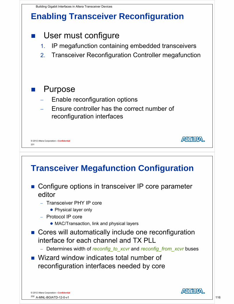
Enabling Transceiver Reconfiguration
User must configure1. IP megafunction containing embedded transceivers
2. Transceiver Reconfiguration Controller megafunctiong g
Purpose Enable reconfiguration options
Ensure controller has the correct number of reconfiguration interfaces
© 2012 Altera Corporation—Confidential
231
Transceiver Megafunction Configuration
Configure options in transceiver IP core parameter dieditor Transceiver PHY IP core
Physical layer only Physical layer only
Protocol IP core MAC/Transaction, link and physical layers
Cores will automatically include one reconfiguration interface for each channel and TX PLL Determines width of reconfig_to_xcvr and reconfig_from_xcvr buses
Wizard window indicates total number of fi ti i t f d d breconfiguration interfaces needed by core
© 2012 Altera Corporation—Confidential
232
Building Gigabit Interfaces in Altera Transceiver Devices
A-MNL-BGIATD-12-0-v1 116
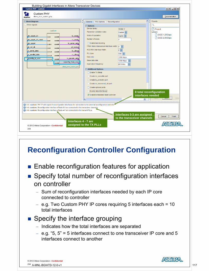
8 total reconfiguration interfaces needed
Interfaces 0-3 are assigned
© 2012 Altera Corporation—Confidential
233
gto the transceiver channels
Interfaces 4 - 7 are assigned to the TX PLLs
Reconfiguration Controller Configuration
Enable reconfiguration features for application
Specify total number of reconfiguration interfaces on controller Sum of reconfiguration interfaces needed by each IP core
connected to controller
T C t PHY IP i i 5 i t f h 10 e.g. Two Custom PHY IP cores requiring 5 interfaces each = 10 total interfaces
Specify the interface grouping Specify the interface grouping Indicates how the total interfaces are separated
e.g. “5, 5” = 5 interfaces connect to one transceiver IP core and 5 g ,interfaces connect to another
© 2012 Altera Corporation—Confidential
234
Building Gigabit Interfaces in Altera Transceiver Devices
A-MNL-BGIATD-12-0-v1 117
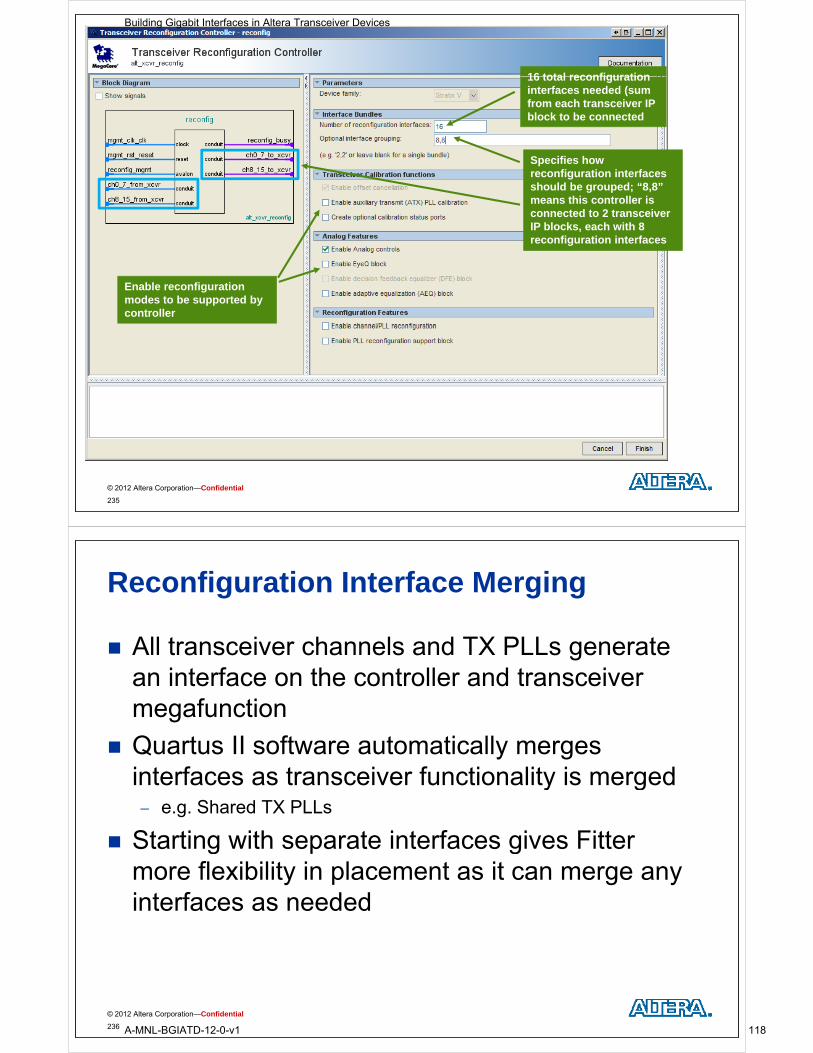
16 total reconfiguration16 total reconfiguration interfaces needed (sum from each transceiver IP block to be connected
Specifies how reconfiguration interfaces should be grouped; “8,8” means this controller ismeans this controller is connected to 2 transceiver IP blocks, each with 8 reconfiguration interfaces
Enable reconfiguration modes to be supported by controller
© 2012 Altera Corporation—Confidential
235
Reconfiguration Interface Merging
All transceiver channels and TX PLLs generate an interface on the controller and transceiver megafunction
Quartus II software automatically merges interfaces as transceiver functionality is mergedy g e.g. Shared TX PLLs
Starting with separate interfaces gives Fitter g p gmore flexibility in placement as it can merge any interfaces as needed
© 2012 Altera Corporation—Confidential
236
Building Gigabit Interfaces in Altera Transceiver Devices
A-MNL-BGIATD-12-0-v1 118
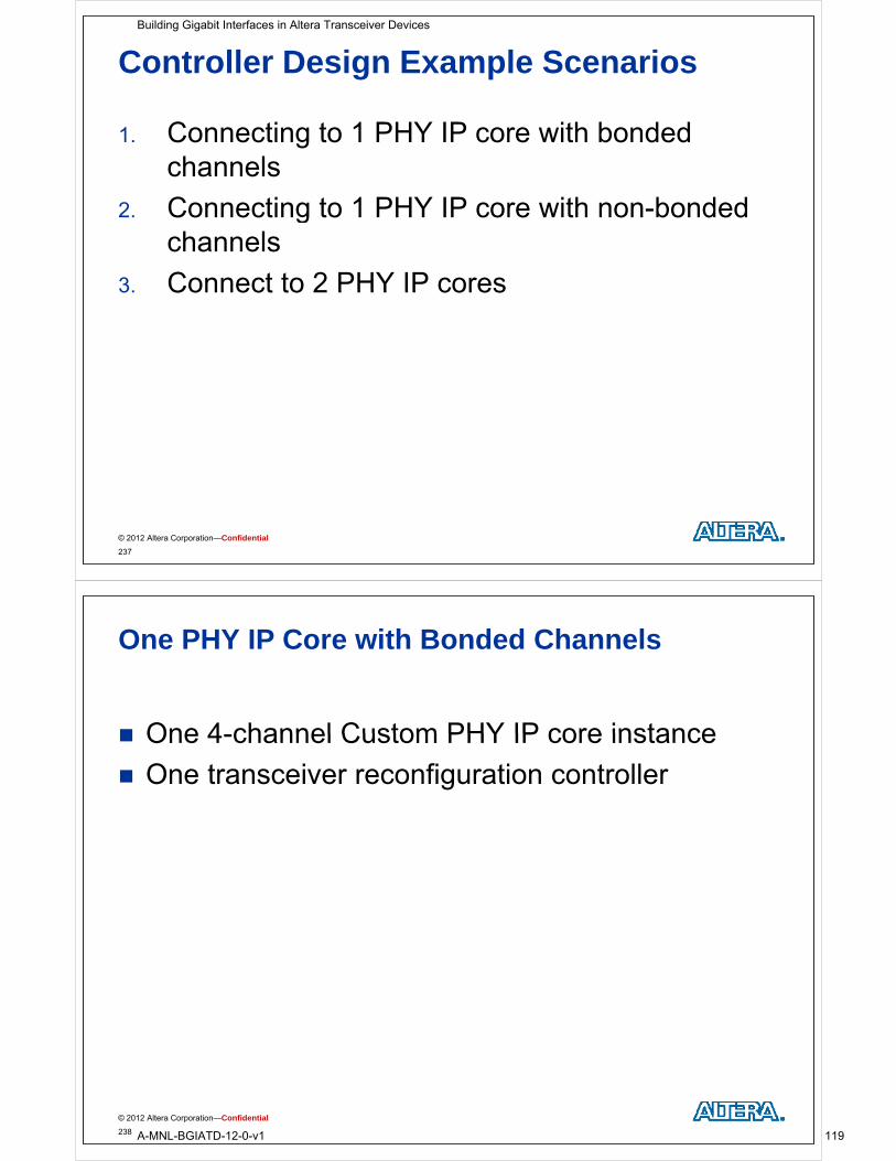
Controller Design Example Scenarios
1. Connecting to 1 PHY IP core with bonded channels
2. Connecting to 1 PHY IP core with non-bonded gchannels
3 Connect to 2 PHY IP cores3. Connect to 2 PHY IP cores
© 2012 Altera Corporation—Confidential
237
One PHY IP Core with Bonded Channels
One 4 channel Custom PHY IP core instance One 4-channel Custom PHY IP core instance
One transceiver reconfiguration controller
© 2012 Altera Corporation—Confidential
238
Building Gigabit Interfaces in Altera Transceiver Devices
A-MNL-BGIATD-12-0-v1 119
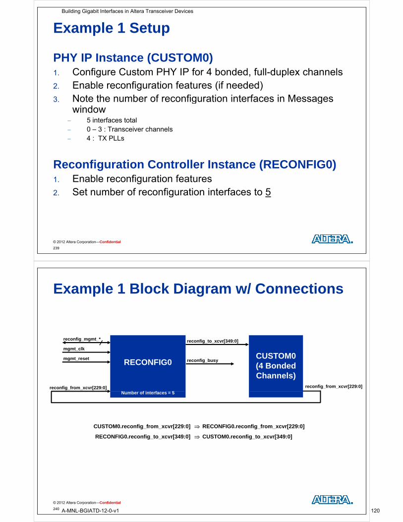
Example 1 Setup
PHY IP Instance (CUSTOM0)C fi C t PHY IP f 4 b d d f ll d l h l1. Configure Custom PHY IP for 4 bonded, full-duplex channels
2. Enable reconfiguration features (if needed)3 Note the number of reconfiguration interfaces in Messages3. Note the number of reconfiguration interfaces in Messages
window 5 interfaces total 0 – 3 : Transceiver channels0 3 : Transceiver channels 4 : TX PLLs
R fi ti C t ll I t (RECONFIG0)Reconfiguration Controller Instance (RECONFIG0)1. Enable reconfiguration features2 Set number of reconfiguration interfaces to 52. Set number of reconfiguration interfaces to 5
© 2012 Altera Corporation—Confidential
239
Example 1 Block Diagram w/ Connections
CUSTOM0reconfig busy
reconfig_to_xcvr[349:0]
mgmt_clk
mgmt reset
reconfig_mgmt_*
RECONFIG0 (4 Bonded Channels)
reconfig_busyg _
reconfig_from_xcvr[229:0]
RECONFIG0
N b f i t f 5
reconfig_from_xcvr[229:0]
Number of interfaces = 5
CUSTOM0.reconfig_from_xcvr[229:0] RECONFIG0.reconfig_from_xcvr[229:0]
RECONFIG0.reconfig_to_xcvr[349:0] CUSTOM0.reconfig_to_xcvr[349:0]
© 2012 Altera Corporation—Confidential
240
Building Gigabit Interfaces in Altera Transceiver Devices
A-MNL-BGIATD-12-0-v1 120
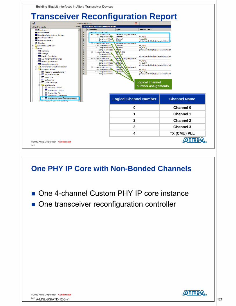
Transceiver Reconfiguration Report
Logical channel number assignments
Logical Channel Number Channel Name
0 Channel 0
C1 Channel 1
2 Channel 2
3 Channel 3
© 2012 Altera Corporation—Confidential
241
4 TX (CMU) PLL
One PHY IP Core with Non-Bonded Channels
One 4 channel Custom PHY IP core instance One 4-channel Custom PHY IP core instance
One transceiver reconfiguration controller
© 2012 Altera Corporation—Confidential
242
Building Gigabit Interfaces in Altera Transceiver Devices
A-MNL-BGIATD-12-0-v1 121

Example 2 Setup
PHY IP Instance (CUSTOM0)1 Configure Custom PHY IP for 4 non bonded full duplex1. Configure Custom PHY IP for 4 non-bonded, full-duplex
channels2. Enable reconfiguration features (if needed)
N t th b f fi ti i t f i M3. Note the number of reconfiguration interfaces in Messages window
8 interfaces total0 3 : Transceiver channels 0 – 3 : Transceiver channels
4 – 7 : TX PLLs
Reconfiguration Controller Instance (RECONFIG0)Reconfiguration Controller Instance (RECONFIG0)1. Configure transceiver reconfiguration controller2. Enable reconfiguration featuresg3. Set number of reconfiguration interfaces to 8
© 2012 Altera Corporation—Confidential
243
Example 2 Block Diagram w/ Connections
CUSTOM0(4 Nonreconfig busy
reconfig_to_xcvr[559:0]
mgmt_clk
mgmt reset
reconfig_mgmt_*
RECONFIG0 (4 Non-Bonded
Channels)
reconfig_busyg _
reconfig_from_xcvr[367:0]
RECONFIG0
Number of interfaces = 8reconfig_from_xcvr[367:0]
Number of interfaces = 8
CUSTOM0.reconfig_from_xcvr[367:0] RECONFIG0.reconfig_from_xcvr[367:0]
RECONFIG0.reconfig_to_xcvr[559:0] CUSTOM0.reconfig_to_xcvr[559:0]
© 2012 Altera Corporation—Confidential
244
Building Gigabit Interfaces in Altera Transceiver Devices
A-MNL-BGIATD-12-0-v1 122
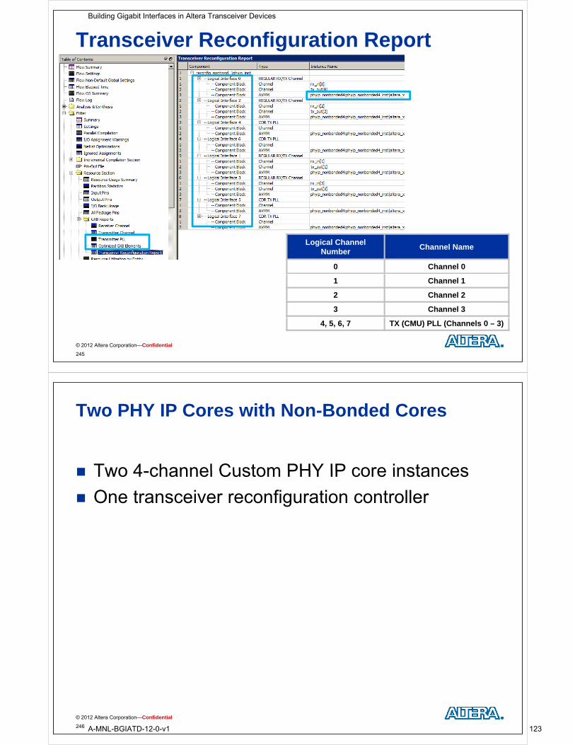
Transceiver Reconfiguration Report
Logical Channel Number
Channel Name
0 Channel 0
1 Channel 1
2 Channel 2
3 Channel 3
© 2012 Altera Corporation—Confidential
245
4, 5, 6, 7 TX (CMU) PLL (Channels 0 – 3)
Two PHY IP Cores with Non-Bonded Cores
Two 4 channel Custom PHY IP core instances Two 4-channel Custom PHY IP core instances
One transceiver reconfiguration controller
© 2012 Altera Corporation—Confidential
246
Building Gigabit Interfaces in Altera Transceiver Devices
A-MNL-BGIATD-12-0-v1 123
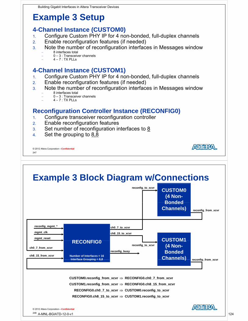
Example 3 Setup4-Channel Instance (CUSTOM0)1. Configure Custom PHY IP for 4 non-bonded, full-duplex channels2 Enable reconfiguration features (if needed)2. Enable reconfiguration features (if needed)3. Note the number of reconfiguration interfaces in Messages window
8 interfaces total 0 – 3 : Transceiver channels 4 – 7 : TX PLLs
4-Channel Instance (CUSTOM1)1. Configure Custom PHY IP for 4 non-bonded, full-duplex channels
f f ( f )2. Enable reconfiguration features (if needed)3. Note the number of reconfiguration interfaces in Messages window
8 interfaces total 0 – 3 : Transceiver channels
4 7 TX PLL 4 – 7 : TX PLLs
Reconfiguration Controller Instance (RECONFIG0)1 Configure transceiver reconfiguration controller1. Configure transceiver reconfiguration controller2. Enable reconfiguration features3. Set number of reconfiguration interfaces to 84. Set the grouping to 8,8
© 2012 Altera Corporation—Confidential
g p g
247
Example 3 Block Diagram w/ConnectionsCUSTOM0
(4 Non-Bonded
reconfig_to_xcvr
Bonded Channels) reconfig_from_xcvr
ch8_15_to_xcvr
CUSTOM1
ch0_7_to_xcvr
mgmt_clk
mgmt_reset
reconfig_mgmt_*
RECONFIG0
reconfig_busy
CUSTOM1(4 Non-Bonded
Channels) reconfig from xcvr
ch8_15_from_xcvr
RECONFIG0
Number of Interfaces = 16Interface Grouping = 8 8
reconfig_to_xcvrch0_7_from_xcvr
Channels) reconfig_from_xcvrInterface Grouping = 8,8
CUSTOM0 reconfig from xcvr RECONFIG0 ch0 7 from xcvrCUSTOM0.reconfig_from_xcvr RECONFIG0.ch0_7_from_xcvr
CUSTOM1.reconfig_from_xcvr RECONFIG0.ch8_15_from_xcvr
RECONFIG0.ch0_7_to_xcvr CUSTOM0.reconfig_to_xcvr
RECONFIG0.ch8 15 to xcvr CUSTOM1.reconfig to xcvr
© 2012 Altera Corporation—Confidential
248
RECONFIG0.ch8_15_to_xcvr CUSTOM1.reconfig_to_xcvr
Building Gigabit Interfaces in Altera Transceiver Devices
A-MNL-BGIATD-12-0-v1 124

Example 3 Logical Channel Number Assignments*
Logical Channel Number Channel Name
0 CUSTOM0 Channel 0
1 CUSTOM0 Ch l 11 CUSTOM0 Channel 1
2 CUSTOM0 Channel 2
3 CUSTOM0 Channel 3
8 CUSTOM1 Channel0
9 CUSTOM1 Channel1
10 CUSTOM1 Channel210 CUSTOM1 Channel2
11 CUSTOM1 Channel3
4, 5, 6, 7 CUSTOM0 CMU PLL
12, 15 CUSTOM1 CMU PLL (0, 3)
13, 14 CUSTOM1 CMU PLL (1, 2)
© 2012 Altera Corporation—Confidential
249
* One possible solution
Agenda
Introduction
Transceiver Reconfiguration Controller
Example Reconfigurations Example Reconfigurations Calibration
PMA Reconfiguration
Introduction to TX PLL Switching
© 2012 Altera Corporation—Confidential
250
Building Gigabit Interfaces in Altera Transceiver Devices
A-MNL-BGIATD-12-0-v1 125
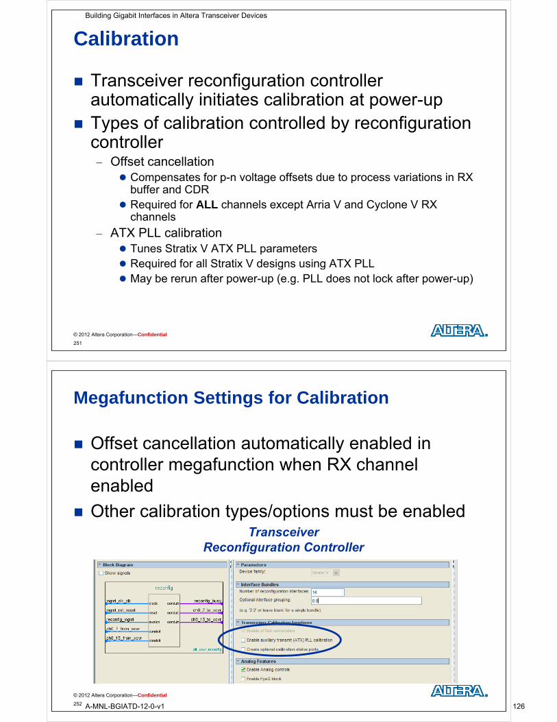
Calibration
Transceiver reconfiguration controller t ti ll i iti t lib ti tautomatically initiates calibration at power-up
Types of calibration controlled by reconfiguration t llcontroller
Offset cancellation Compensates for p-n voltage offsets due to process variations in RXCompensates for p n voltage offsets due to process variations in RX
buffer and CDR Required for ALL channels except Arria V and Cyclone V RX
channels
ATX PLL calibration Tunes Stratix V ATX PLL parameters Required for all Stratix V designs using ATX PLL Required for all Stratix V designs using ATX PLL May be rerun after power-up (e.g. PLL does not lock after power-up)
© 2012 Altera Corporation—Confidential
251
Megafunction Settings for Calibration
Offset cancellation automatically enabled in controller megafunction when RX channel enabled
Other calibration types/options must be enabledTransceiver
Reconfiguration Controller
© 2012 Altera Corporation—Confidential
252
Building Gigabit Interfaces in Altera Transceiver Devices
A-MNL-BGIATD-12-0-v1 126
Performing Calibration
1. Upon power-up, transceiver reconfiguration controller i iti t lib tiinitiates calibration
2. Embedded reset controller triggers reset when complete
M it fi b t t fl b i t t3. Monitor reconfig_busy output flag or busy register to determine when controller is done
4 Monitor tx ready and rx ready signals to learn when4. Monitor tx_ready and rx_ready signals to learn when channels are ready to send/receive data
© 2012 Altera Corporation—Confidential
253
Agenda
Introduction
Transceiver Reconfiguration Controller
Example Reconfigurations Example Reconfigurations Calibration
PMA Reconfiguration
Introduction to TX PLL Switching
© 2012 Altera Corporation—Confidential
254
Building Gigabit Interfaces in Altera Transceiver Devices
A-MNL-BGIATD-12-0-v1 127
PMA Reconfiguration
Selects from thousands of transmit and receive PMA analog settings dynamically
Use to Improve signal integrity during in-system tests and debuggingp g g y g y gg g
Fine tune transmit/receive buffers according to specific board/system conditions
Manually adjust settings to achieve target BER in FPGA or Manually adjust settings to achieve target BER in FPGA or upstream device
© 2012 Altera Corporation—Confidential
255
Configurable PMA Settings
Output differential voltage (VOD)
Pre-emphasis support
Equalization Equalization
Equalizer DC gain
© 2012 Altera Corporation—Confidential
256
Building Gigabit Interfaces in Altera Transceiver Devices
A-MNL-BGIATD-12-0-v1 128
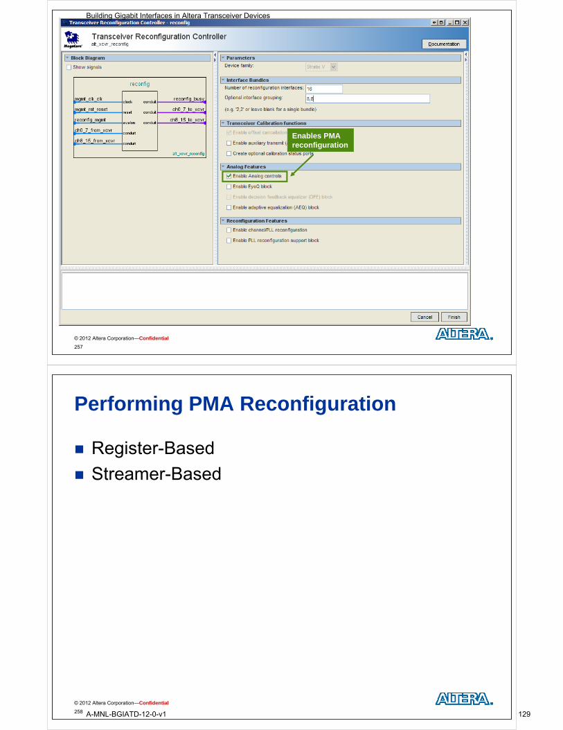
Enables PMA reconfiguration
© 2012 Altera Corporation—Confidential
257
Performing PMA Reconfiguration
Register-Based
Streamer-Based
© 2012 Altera Corporation—Confidential
258
Building Gigabit Interfaces in Altera Transceiver Devices
A-MNL-BGIATD-12-0-v1 129
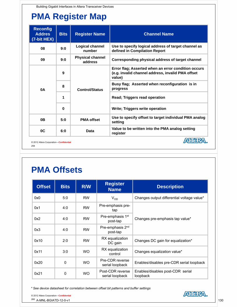
PMA Register MapReconfigAddres
(7-bit HEX)Bits Register Name Channel Name
(7 bit HEX)
08 9:0Logical channel
numberUse to specify logical address of target channel as defined in Compilation Report
09 9 0Physical channel
C di h i l dd f t t h l09 9:0Physical channel
addressCorresponding physical address of target channel
9Error flag; Asserted when an error condition occurs (e.g. invalid channel address, invalid PMA offset
l )
0A Control/Status
value)
8Busy flag; Asserted when reconfiguration is in progress
1 Read; Triggers read operation
0 Write; Triggers write operation
0B 5:0 PMA offsetUse to specify offset to target individual PMA analog setting
0C 6:0 DataValue to be written into the PMA analog setting
© 2012 Altera Corporation—Confidential
259
0C 6:0 Dataregister
PMA Offsets
Offset Bits R/WRegister
NameDescription
0x0 5:0 RW VOD Changes output differential voltage value*
0x1 4:0 RWPre-emphasis pre-
tapp
Changes pre-emphasis tap value*0x2 4:0 RWPre-emphasis 1st
post-tap
0x3 4:0 RWPre-emphasis 2nd
0x3 4:0 RWpost-tap
0x10 2:0 RWRX equalization
DC gainChanges DC gain for equalization*
RX li ti0x11 3:0 WO
RX equalizationcontrol
Changes equalization value*
0x20 0 WOPre-CDR reverse serial loopback
Enables/disables pre-CDR serial loopbackp
0x21 0 WOPost-CDR reverse
serial loopbackEnables/disables post-CDR serial loopback
© 2012 Altera Corporation—Confidential
260
* See device datasheet for correlation between offset bit patterns and buffer settings
Building Gigabit Interfaces in Altera Transceiver Devices
A-MNL-BGIATD-12-0-v1 130
Agenda
Introduction
Transceiver Reconfiguration Controller
Example Reconfigurations Example Reconfigurations Calibration
PMA Reconfiguration
Introduction to TX PLL Switching
© 2012 Altera Corporation—Confidential
261
TX PLL Switching
Enable multiple TX PLLs in one PHY IP instance to support multiple unrelated data rates May or may not include protocol (functional mode) change
Change data rates by switching from one TX PLL to other Without reconfiguring PLLs
Adds flexibility to design by supporting multiple data rates with same transceiver channels
* This is one aspect of channel reconfiguration. For more information on other types of channel reconfiguration, please seethe device handbook and the PHY IP user guide.
© 2012 Altera Corporation—Confidential
262
Building Gigabit Interfaces in Altera Transceiver Devices
A-MNL-BGIATD-12-0-v1 131
Channel & PLL Reconfiguration Concepts
Memory initialization file (MIF)
Input reference clocks
Logical reference index Logical reference index
© 2012 Altera Corporation—Confidential
263
Memory Initialization File
Used during reconfiguration to store settings for a single t i h l d/ PLLtransceiver channel and/or PLL Stores a single transceiver state
To support multiple transceiver configurations, you must generate and store multiple MIFs
Generated automatically by Quartus II Assembler based on transceiver PHY IP core settingson transceiver PHY IP core settings
For design implementation, configure transceiver IP core for each set of reconfiguration options and recompilefor each set of reconfiguration options and recompile Each recompilation creates a reconfiguration MIF
For faster compile times, consider creating a simplified reference or t l t d itemplate design
Reconfigure channels by writing new MIF into channel
© 2012 Altera Corporation—Confidential
264
Building Gigabit Interfaces in Altera Transceiver Devices
A-MNL-BGIATD-12-0-v1 132
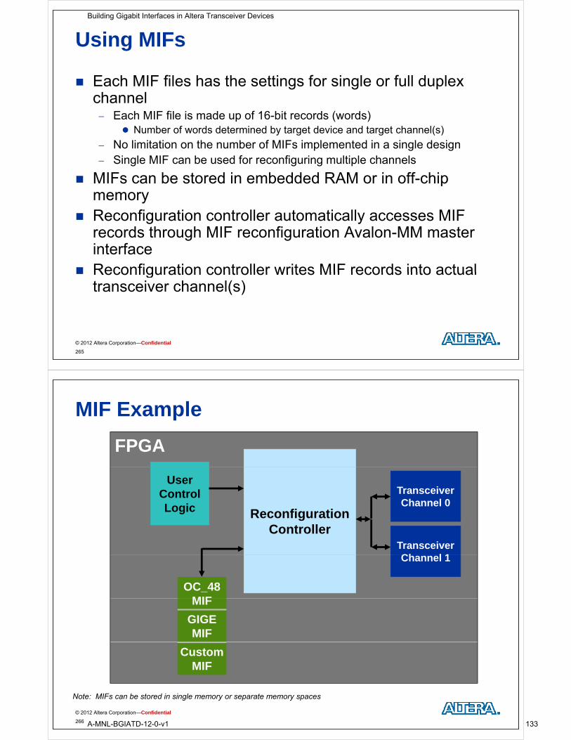
Using MIFs
Each MIF files has the settings for single or full duplex channelchannel Each MIF file is made up of 16-bit records (words)
Number of words determined by target device and target channel(s)
N li it ti th b f MIF i l t d i i l d i No limitation on the number of MIFs implemented in a single design Single MIF can be used for reconfiguring multiple channels
MIFs can be stored in embedded RAM or in off-chip pmemory
Reconfiguration controller automatically accesses MIF d th h MIF fi ti A l MM trecords through MIF reconfiguration Avalon-MM master
interface Reconfiguration controller writes MIF records into actual Reconfiguration controller writes MIF records into actual
transceiver channel(s)
© 2012 Altera Corporation—Confidential
265
MIF Example
FPGA
UserControlLogic R fi ti
Transceiver Channel 0Logic Reconfiguration
ControllerTransceiver Ch l 1Channel 1
OC_48 MIFMIF
GIGEMIF
CustomMIF
© 2012 Altera Corporation—Confidential
266
Note: MIFs can be stored in single memory or separate memory spaces
Building Gigabit Interfaces in Altera Transceiver Devices
A-MNL-BGIATD-12-0-v1 133
Input Reference Clocks
PHY IP clock sources for TX PLLs and RX CDRsT i f ti t t 5 diff t i t Transceiver megafunction supports up to 5 different input reference clocks when channel and PLL reconfiguration enabled
Changing input reference clocks changes input clock frequency to PLLs and CDRs Allows support for wider variety of data rates vs. changing PLL settings
alone
© 2012 Altera Corporation—Confidential
267
TX PLL Logical Index Number
Reference number assigned to TX PLLs within a PHY IP instancePHY IP instance Provides a way to refer to TX PLL by logical index number Knowing actual physical location of TX PLL not required
Supported values are 0 - 3 PHY IP instance using single TX PLL
TX PLL automatically assigned logical index 0 TX PLL automatically assigned logical index 0 PHY IP instance using multiple PLLs
User must assign logical index 0 - 3 to each TX PLL
Uses Uses Indicate the TX PLL to which the transceiver channel is “listening” Facilitate changing channel data rates by switching to other TX g g y g
PLL in transceiver block
© 2012 Altera Corporation—Confidential
268
Building Gigabit Interfaces in Altera Transceiver Devices
A-MNL-BGIATD-12-0-v1 134
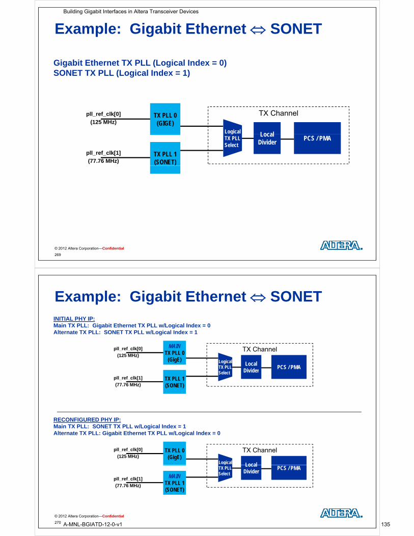
Example: Gigabit Ethernet SONET
Gigabit Ethernet TX PLL (Logical Index = 0)SONET TX PLL (L i l I d 1)SONET TX PLL (Logical Index = 1)
pll_ref_clk[0]
(125 MHz)
TX Channel
Local
TX PLL 0(GIGE)
Logical
pll_ref_clk[1]
(77.76 MHz)
PCS / PMALocal
Divider
TX PLL 1(SONET)
gTX PLL Select
( )
© 2012 Altera Corporation—Confidential
269
Example: Gigabit Ethernet SONETINITIAL PHY IP:Main TX PLL: Gigabit Ethernet TX PLL w/Logical Index = 0Alternate TX PLL: SONET TX PLL w/Logical Index = 1
pll_ref_clk[0]
(125 MHz)TX Channel
PCS / PMALocal
Divider
MAINTX PLL 0
(GigE) Logical TX PLL
pll_ref_clk[1]
(77.76 MHz)
Divider
TX PLL 1(SONET)
Select
RECONFIGURED PHY IP:Main TX PLL: SONET TX PLL w/Logical Index = 1Alternate TX PLL: Gigabit Ethernet TX PLL w/Logical Index = 0Alternate TX PLL: Gigabit Ethernet TX PLL w/Logical Index = 0
pll_ref_clk[0]
(125 MHz)TX Channel
Local
TX PLL 0(GigE)
Logical
pll_ref_clk[1]
(77.76 MHz)
PCS / PMALocal
DividerMAIN
TX PLL 1(SONET)
gTX PLL Select
© 2012 Altera Corporation—Confidential
270
Building Gigabit Interfaces in Altera Transceiver Devices
A-MNL-BGIATD-12-0-v1 135
More Details on Channel & PLL Reconfiguration
See Appendix
Online documentation Stratix V Device Handbook, Volume 3, Chapter 6: Dynamic
Reconfiguration in Stratix V Devices
Arria V Device Handbook, Volume 3, Chapter 7: Dynamic Reconfiguration in Arria V DevicesReconfiguration in Arria V Devices
Altera Transceiver PHY IP Core User Guide
© 2012 Altera Corporation—Confidential
271
Test Your Knowledge
1. A Transceiver Reconfiguration Controller is required for transceiver designs that use what resources?A. All RX channels and ATX PLLstransceiver designs that use what resources?
2. What 2 types of calibration are performed by the Transceiver Reconfiguration Controller at power-up?
A. Offset cancellation and ATX PLL calibration
3. The number of reconfiguration interfaces on a PHY IP core is based on what resources in the PHY IP core?
A. The number of transceiver channels and TX PLLs
© 2012 Altera Corporation—Confidential
272
Building Gigabit Interfaces in Altera Transceiver Devices
A-MNL-BGIATD-12-0-v1 136

Building Gigabit Interfaces inBuilding Gigabit Interfaces in Altera Transceiver DevicesT i D i B t P tiTransceiver Design Best Practices
© 2012 Altera Corporation—Confidential
Transceiver Design Best Practices
Resource optimization
Planning reset control
Planning transceiver reconfiguration Planning transceiver reconfiguration
PHY IP versions
© 2012 Altera Corporation—Confidential
274
Building Gigabit Interfaces in Altera Transceiver Devices
A-MNL-BGIATD-12-0-v1 137

Resource Optimization
PLLs
Clocking
Channel placement Channel placement
Pin connection guidelines
© 2012 Altera Corporation—Confidential
275
Choosing the Best PLL (ATX PLL)
LC-based PLL Availability Availability
Stratix V devices only One for every three channels in supported devices
Pros Pros Best performance Increases channel utilization as it frees up a Channel PLL
C Cons Affected by frequency holes due to tuning
e.g. 7-8 G; 3.5-4 G; 1.8-2 G; < 1 GTop versus bottom ATX PLLs in transceiver bank have different supported Top versus bottom ATX PLLs in transceiver bank have different supported ranges See Stratix V Errata for details
Needs calibration due to narrow tuning range
Recommended for all cases when data rate is supported
© 2012 Altera Corporation—Confidential
276
Building Gigabit Interfaces in Altera Transceiver Devices
A-MNL-BGIATD-12-0-v1 138
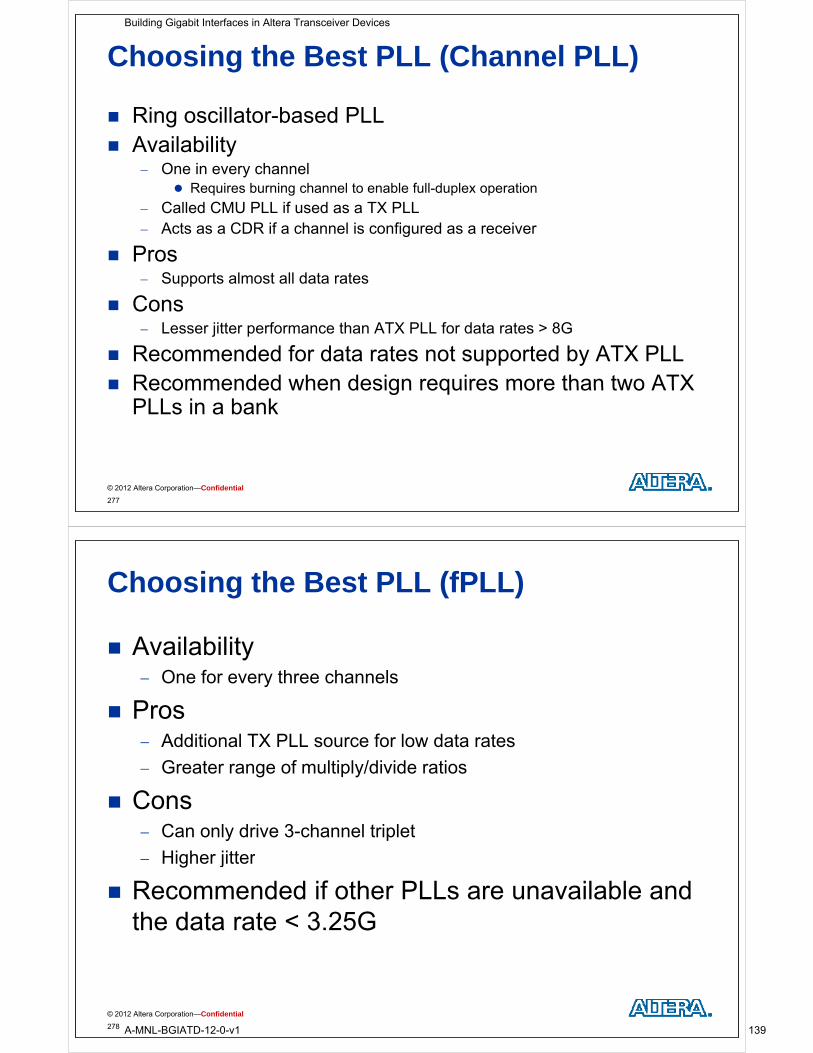
Choosing the Best PLL (Channel PLL)
Ring oscillator-based PLLA il bilit Availability One in every channel
Requires burning channel to enable full-duplex operation
Called CMU PLL if used as a TX PLL Acts as a CDR if a channel is configured as a receiver
Pros Supports almost all data rates
ConsLesser jitter performance than ATX PLL for data rates > 8G Lesser jitter performance than ATX PLL for data rates > 8G
Recommended for data rates not supported by ATX PLL Recommended when design requires more than two ATX Recommended when design requires more than two ATX
PLLs in a bank
© 2012 Altera Corporation—Confidential
277
Choosing the Best PLL (fPLL)
Availability One for every three channels
Pros Additional TX PLL source for low data rates
Greater range of multiply/divide ratios
Cons Can only drive 3-channel triplet
Hi h jitt Higher jitter
Recommended if other PLLs are unavailable and th d t t 3 25Gthe data rate < 3.25G
© 2012 Altera Corporation—Confidential
278
Building Gigabit Interfaces in Altera Transceiver Devices
A-MNL-BGIATD-12-0-v1 139
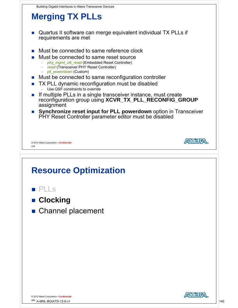
Merging TX PLLs
Quartus II software can merge equivalent individual TX PLLs if requirements are met
Must be connected to same reference clock Must be connected to same reset sourceMust be connected to same reset source
phy_mgmt_clk_reset (Embedded Reset Controller) reset (Transceiver PHY Reset Controller) pll_powerdown (Custom)
Must be connected to same reconfiguration controller Must be connected to same reconfiguration controller TX PLL dynamic reconfiguration must be disabled
Use QSF constraints to override
If multiple PLLs in a single transceiver instance must create If multiple PLLs in a single transceiver instance, must create reconfiguration group using XCVR_TX_PLL_RECONFIG_GROUPassignment
Synchronize reset input for PLL powerdown option in Transceiver y p p pPHY Reset Controller parameter editor must be disabled
© 2012 Altera Corporation—Confidential
279
Resource Optimization
PLLs
Clocking
Channel placement Channel placement
© 2012 Altera Corporation—Confidential
280
Building Gigabit Interfaces in Altera Transceiver Devices
A-MNL-BGIATD-12-0-v1 140
Why Is Understanding Clocking Important?
Maximize transceiver bank usage
Maximize clocking resources
Understand and avoid “no-fits” when mergingUnderstand and avoid no fits when merging multiple protocols or data rates Within single transceiver bankg
On same side of chip
Reduce TX jitter and skewj
Build PCS logic for PMA Direct mode channels
© 2012 Altera Corporation—Confidential
281
Transceiver Clocking
Reference clocks
Internal clocking (TX clock network)
FPGA fabric-transceiver clocks FPGA fabric transceiver clocks
© 2012 Altera Corporation—Confidential
282
Building Gigabit Interfaces in Altera Transceiver Devices
A-MNL-BGIATD-12-0-v1 141
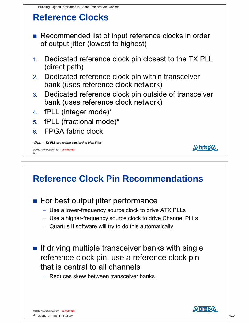
Reference Clocks
Recommended list of input reference clocks in order of output jitter (lowest to highest)of output jitter (lowest to highest)
1. Dedicated reference clock pin closest to the TX PLL p(direct path)
2. Dedicated reference clock pin within transceiver bank (uses reference clock network)
3. Dedicated reference clock pin outside of transceiver b k ( f l k t k)bank (uses reference clock network)
4. fPLL (integer mode)*fPLL (f ti l d )*5. fPLL (fractional mode)*
6. FPGA fabric clock
© 2012 Altera Corporation—Confidential
283
* fPLL → TX PLL cascading can lead to high jitter
Reference Clock Pin Recommendations
For best output jitter performancep j p Use a lower-frequency source clock to drive ATX PLLs
Use a higher-frequency source clock to drive Channel PLLs
Quartus II software will try to do this automatically
If driving multiple transceiver banks with single reference clock pin, use a reference clock pin p , pthat is central to all channels Reduces skew between transceiver banks
© 2012 Altera Corporation—Confidential
284
Building Gigabit Interfaces in Altera Transceiver Devices
A-MNL-BGIATD-12-0-v1 142
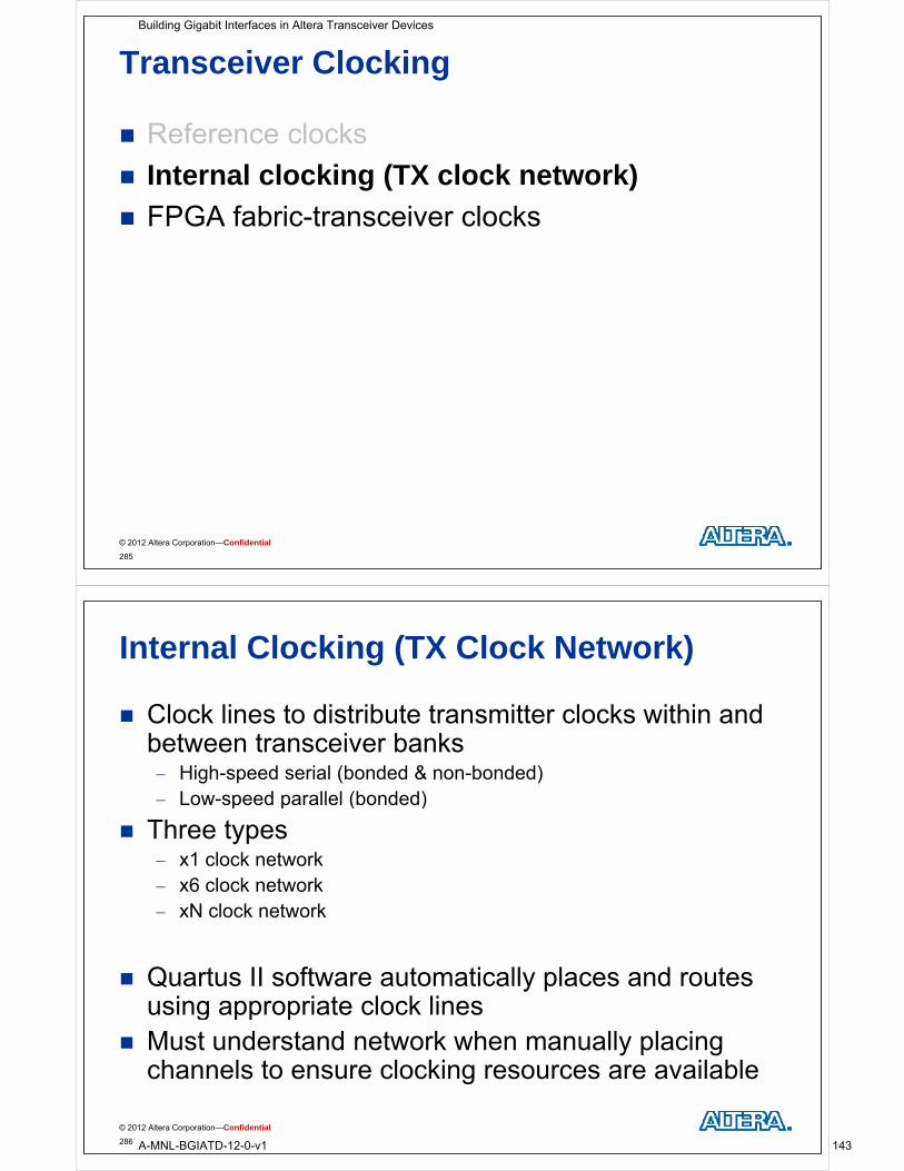
Transceiver Clocking
Reference clocks
Internal clocking (TX clock network)
FPGA fabric-transceiver clocks FPGA fabric transceiver clocks
© 2012 Altera Corporation—Confidential
285
Internal Clocking (TX Clock Network)
Clock lines to distribute transmitter clocks within and between transceiver banksbetween transceiver banks High-speed serial (bonded & non-bonded) Low-speed parallel (bonded)p p ( )
Three types x1 clock network x6 clock network xN clock network
Quartus II software automatically places and routes using appropriate clock linesg pp p
Must understand network when manually placing channels to ensure clocking resources are available
© 2012 Altera Corporation—Confidential
286
Building Gigabit Interfaces in Altera Transceiver Devices
A-MNL-BGIATD-12-0-v1 143
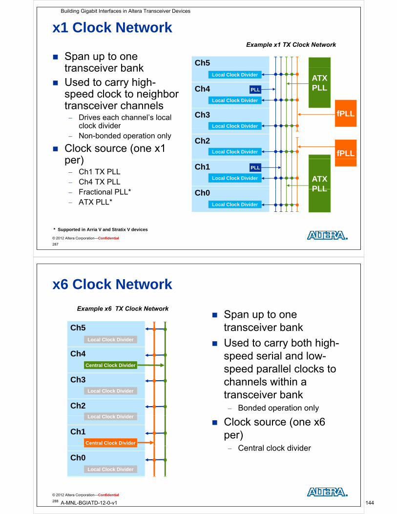
x1 Clock Network
Ch5 Span up to one
transceiver bank
Example x1 TX Clock Network
Ch4
transceiver bank Used to carry high-
speed clock to neighbor
Local Clock Divider
PLL
ATX PLL
Ch3
p gtransceiver channels Drives each channel’s local
clock divider Local Clock Divider
Local Clock Divider
fPLL
Ch2 Non-bonded operation only
Clock source (one x1 per)
Local Clock Divider fPLL
Ch1per) Ch1 TX PLL Ch4 TX PLL
F ti l PLL*
Local Clock Divider
PLL
ATX PLLCh0 Fractional PLL*
ATX PLL* Local Clock Divider
PLL
© 2012 Altera Corporation—Confidential
287
* Supported in Arria V and Stratix V devices
x6 Clock Network
Span up to one t i b k
Example x6 TX Clock Network
C transceiver bank
Used to carry both high-speed serial and low
Ch5
Ch4
Local Clock Divider
speed serial and low-speed parallel clocks to channels within a
Ch4
Ch3
Central Clock Divider
channels within a transceiver bank Bonded operation onlyCh2
Local Clock Divider
L l Cl k Di id
Clock source (one x6 per)
C t l l k di id
Ch1
Local Clock Divider
Central Clock Divider Central clock divider
Ch0Local Clock Divider
© 2012 Altera Corporation—Confidential
288
Building Gigabit Interfaces in Altera Transceiver Devices
A-MNL-BGIATD-12-0-v1 144
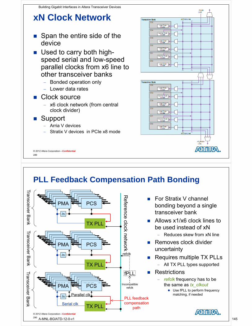
xN Clock Network
Span the entire side of the devicedevice
Used to carry both high-speed serial and low-speed p pparallel clocks from x6 line to other transceiver banks
Bonded operation only Bonded operation only Lower data rates
Clock source x6 clock network (from central
clock divider)
Support Support Arria V devices Stratix V devices in PCIe x8 mode
© 2012 Altera Corporation—Confidential
289
PLL Feedback Compensation Path Bonding
For Stratix V channel bonding beyond a single
Refe
Transce
PCSPCSPCSPMAPMAPMA PCSPCSPMAPMA PCSPMA bonding beyond a single
transceiver bank
Allows x1/x6 clock lines to
rence clo
iver Bank TX PLL
/n
be used instead of xN Reduces skew from xN line
Removes clock divider
ock netwo
PCSPCSPCSPMAPMAPMA PCSPCSPMAPMA PCSPMA
TX PLLT
ransc
uncertainty
Requires multiple TX PLLsAll TX PLL t t d
ork
PCSPMA PCSPMA
TX PLL
/n
ceiver Ban
refclk
All TX PLL types supported
Restrictions refclk frequency has to be PCSPCSPCS
PMAPMAPMA PCSPCSPMAPMA
TX PLLkT
rans
fPLL
the same as tx_clkout Use fPLL to perform frequency
matching, if needed
PCSPMA PCSPCSPMAPMA PCSPMA
/n
sceiver Ba PLL feedback
ti
Parallel clk
Incompatiblerefclk
© 2012 Altera Corporation—Confidential
290
TX PLL
nk compensation path
Serial clk
Building Gigabit Interfaces in Altera Transceiver Devices
A-MNL-BGIATD-12-0-v1 145
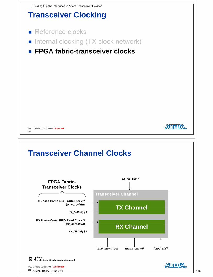
Transceiver Clocking
Reference clocks
Internal clocking (TX clock network)
FPGA fabric-transceiver clocks FPGA fabric transceiver clocks
© 2012 Altera Corporation—Confidential
291
Transceiver Channel Clocks
pll_ref_clk[ ]FPGA Fabric-
Transceiver Clocks
Transceiver Channel
TX ChannelTX Phase Comp FIFO Write Clock(1)
(tx_coreclkin)TX Channel
tx_clkout[ ]
RX Phase Comp FIFO Read Clock(1)
(rx coreclkin)RX Channel
rx_clkout[ ]
(rx_coreclkin)
( ) O
phy_mgmt_clk mgmt_clk_clk fixed_clk(2)
© 2012 Altera Corporation—Confidential
292
(1) Optional(2) PCIe electrical idle clock (not discussed)
Building Gigabit Interfaces in Altera Transceiver Devices
A-MNL-BGIATD-12-0-v1 146
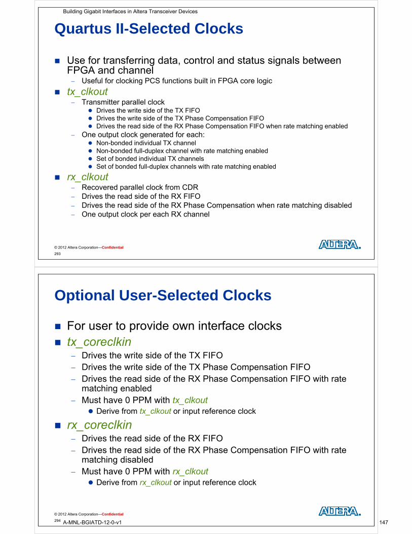
Quartus II-Selected Clocks
Use for transferring data, control and status signals between FPGA and channelFPGA and channel Useful for clocking PCS functions built in FPGA core logic
tx_clkoutTransmitter parallel clock Transmitter parallel clock Drives the write side of the TX FIFO Drives the write side of the TX Phase Compensation FIFO Drives the read side of the RX Phase Compensation FIFO when rate matching enabled
One output clock generated for each: One output clock generated for each: Non-bonded individual TX channel Non-bonded full-duplex channel with rate matching enabled Set of bonded individual TX channels S t f b d d f ll d l h l ith t t hi bl d Set of bonded full-duplex channels with rate matching enabled
rx_clkout Recovered parallel clock from CDR
Drives the read side of the RX FIFO Drives the read side of the RX FIFO Drives the read side of the RX Phase Compensation when rate matching disabled One output clock per each RX channel
© 2012 Altera Corporation—Confidential
293
Optional User-Selected Clocks
For user to provide own interface clockslki tx_coreclkin
Drives the write side of the TX FIFO Drives the write side of the TX Phase Compensation FIFODrives the write side of the TX Phase Compensation FIFO Drives the read side of the RX Phase Compensation FIFO with rate
matching enabledMust have 0 PPM with tx clkout Must have 0 PPM with tx_clkout Derive from tx_clkout or input reference clock
rx_coreclkin Drives the read side of the RX FIFO Drives the read side of the RX Phase Compensation FIFO with rate
matching disabledg Must have 0 PPM with rx_clkout
Derive from rx_clkout or input reference clock
© 2012 Altera Corporation—Confidential
294
Building Gigabit Interfaces in Altera Transceiver Devices
A-MNL-BGIATD-12-0-v1 147
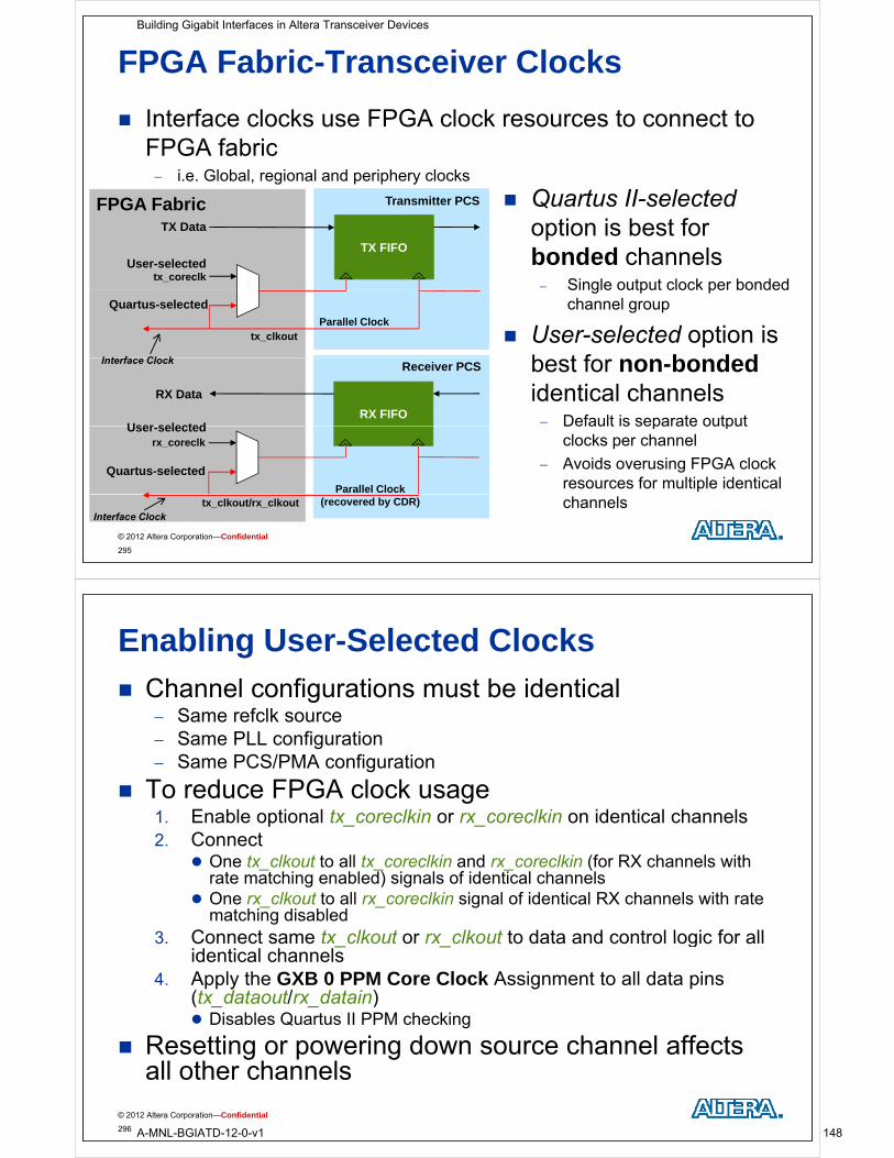
FPGA Fabric-Transceiver Clocks
Interface clocks use FPGA clock resources to connect to FPGA fabricFPGA fabric i.e. Global, regional and periphery clocks
FPGA Fabric Transmitter PCS Quartus II-selectedti i b t f
TX FIFOUser-selected
TX Data
tx_coreclk
option is best for bonded channels Single output clock per bonded
Parallel Clock
Quartus-selected
tx_clkout
Single output clock per bonded channel group
User-selected option is b t f b d dI t f Cl k
RX FIFOUser selected
RX Data
Receiver PCS best for non-bondedidentical channels Default is separate output
Interface Clock
Parallel Clock
Quartus-selected
User-selectedrx_coreclk
Default is separate output clocks per channel
Avoids overusing FPGA clock resources for multiple identical
© 2012 Altera Corporation—Confidential
(recovered by CDR)tx_clkout/rx_clkout channelsInterface Clock
295
Enabling User-Selected Clocks
Channel configurations must be identical Same refclk source
S f Same PLL configuration Same PCS/PMA configuration
To reduce FPGA clock usageg1. Enable optional tx_coreclkin or rx_coreclkin on identical channels2. Connect
One tx clkout to all tx coreclkin and rx coreclkin (for RX channels with _ _ _ (rate matching enabled) signals of identical channels
One rx_clkout to all rx_coreclkin signal of identical RX channels with rate matching disabled
3 Connect same tx clkout or rx clkout to data and control logic for all3. Connect same tx_clkout or rx_clkout to data and control logic for all identical channels
4. Apply the GXB 0 PPM Core Clock Assignment to all data pins (tx dataout/rx datain)( _ _ ) Disables Quartus II PPM checking
Resetting or powering down source channel affects all other channels
© 2012 Altera Corporation—Confidential
all other channels
296
Building Gigabit Interfaces in Altera Transceiver Devices
A-MNL-BGIATD-12-0-v1 148

FPGA Clocks for Stratix V 10G Channels
10G channels A clock divider or fPLL may be necessary to generate the right
frequency to drive tx_coreclkin or rx_coreclkin based on the RX/TX Gearbox ratio and channel configurationRX/TX Gearbox ratio and channel configuration
See Transceiver Configurations in Stratix V Devices chapter in Stratix V Handbook
RX FIFO
Transceiver
Data &
READWRITE
Data & Control
FPGA
Low Speed PCS Clock
User Clock
© 2012 Altera Corporation—Confidential
297
Resource Optimization
PLLs
Clocking
Channel placement Channel placement
© 2012 Altera Corporation—Confidential
298
Building Gigabit Interfaces in Altera Transceiver Devices
A-MNL-BGIATD-12-0-v1 149
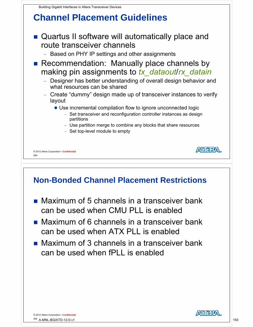
Channel Placement Guidelines
Quartus II software will automatically place and t t i h lroute transceiver channels
Based on PHY IP settings and other assignments
Recommendation: Manually place channels by Recommendation: Manually place channels by making pin assignments to tx_dataout/rx_datain Designer has better understanding of overall design behavior andDesigner has better understanding of overall design behavior and
what resources can be shared Create “dummy” design made up of transceiver instances to verify
layoutlayout Use incremental compilation flow to ignore unconnected logic
Set transceiver and reconfiguration controller instances as design partitionspartitions
Use partition merge to combine any blocks that share resources Set top-level module to empty
© 2012 Altera Corporation—Confidential
299
Non-Bonded Channel Placement Restrictions
Maximum of 5 channels in a transceiver bank can be used when CMU PLL is enabled
Maximum of 6 channels in a transceiver bank can be used when ATX PLL is enabled
Maximum of 3 channels in a transceiver bank Maximum of 3 channels in a transceiver bank can be used when fPLL is enabled
© 2012 Altera Corporation—Confidential
300
Building Gigabit Interfaces in Altera Transceiver Devices
A-MNL-BGIATD-12-0-v1 150
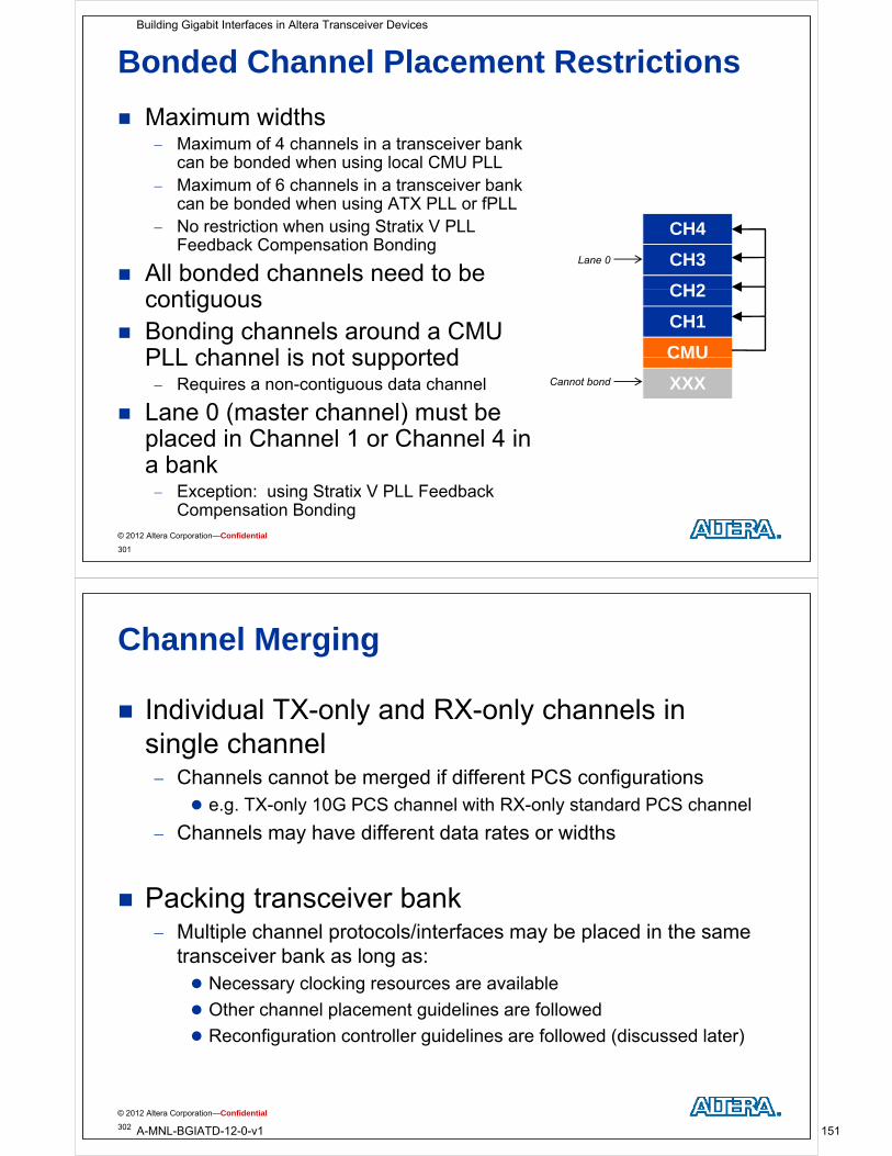
Bonded Channel Placement Restrictions
Maximum widths Maximum of 4 channels in a transceiver bank
can be bonded when using local CMU PLL Maximum of 6 channels in a transceiver bank
can be bonded when using ATX PLL or fPLLN t i ti h i St ti V PLL No restriction when using Stratix V PLL Feedback Compensation Bonding
All bonded channels need to be
CH4
CH3
CH2
Lane 0
contiguous Bonding channels around a CMU
PLL channel is not supported
CH2
CH1
CMUPLL channel is not supported Requires a non-contiguous data channel
Lane 0 (master channel) must be
CMU
XXXCannot bond
placed in Channel 1 or Channel 4 in a bank Exception: using Stratix V PLL Feedback
© 2012 Altera Corporation—Confidential
Exception: using Stratix V PLL Feedback Compensation Bonding
301
Channel Merging
Individual TX-only and RX-only channels in single channel Channels cannot be merged if different PCS configurations
TX l 10G PCS h l ith RX l t d d PCS h l e.g. TX-only 10G PCS channel with RX-only standard PCS channel
Channels may have different data rates or widths
Packing transceiver bank Multiple channel protocols/interfaces may be placed in the sameMultiple channel protocols/interfaces may be placed in the same
transceiver bank as long as: Necessary clocking resources are available
O h h l l id li f ll d Other channel placement guidelines are followed
Reconfiguration controller guidelines are followed (discussed later)
© 2012 Altera Corporation—Confidential
302
Building Gigabit Interfaces in Altera Transceiver Devices
A-MNL-BGIATD-12-0-v1 151
Transceiver Design Best Practices
Resource optimization
Planning reset control
Planning transceiver reconfiguration Planning transceiver reconfiguration
PHY IP versions
Pi ti id li Pin connection guidelines
© 2012 Altera Corporation—Confidential
303
Reset Solutions (Review)
Embedded Reset Controller Available by default with most of the Transceiver PHY IP cores
Avalon Memory-Mapped reset registers Read and write to control and status registers using embedded
controller to reset channels
Available by default with most of the Transceiver PHY IP cores Available by default with most of the Transceiver PHY IP cores
Transceiver PHY Reset Controller IP coreAvailable in MegaWizard Plug In Manager Available in MegaWizard Plug-In Manager
CustomUser designs custom reset logic in the FPGA fabric User designs custom reset logic in the FPGA fabric
Transceiver core provides necessary signals for implementation
© 2012 Altera Corporation—Confidential
304
Building Gigabit Interfaces in Altera Transceiver Devices
A-MNL-BGIATD-12-0-v1 152
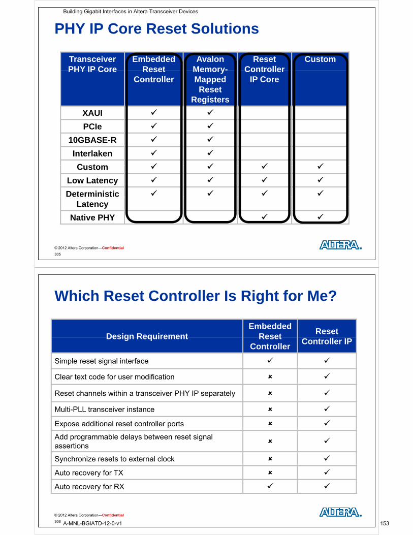
PHY IP Core Reset Solutions
Transceiver PHY IP Core
Embedded Reset
Avalon Memory-
Reset Controller
CustomPHY IP Core Reset
ControllerMemoryMapped Reset
Registers
Controller IP Core
Registers
XAUI
PCIe
10GBASE-R
Interlaken
C t Custom
Low Latency
Deterministic Latency
Native PHY
© 2012 Altera Corporation—Confidential
305
Which Reset Controller Is Right for Me?
Design RequirementEmbedded
ResetReset
Design Requirement Reset Controller
Controller IP
Simple reset signal interface
Clear text code for user modification
Reset channels within a transceiver PHY IP separately
Multi-PLL transceiver instance
Expose additional reset controller ports
Add programmable delays between reset signal assertions
Synchronize resets to external clock
Auto recovery for TX
Auto recovery for RX
© 2012 Altera Corporation—Confidential
306
Building Gigabit Interfaces in Altera Transceiver Devices
A-MNL-BGIATD-12-0-v1 153
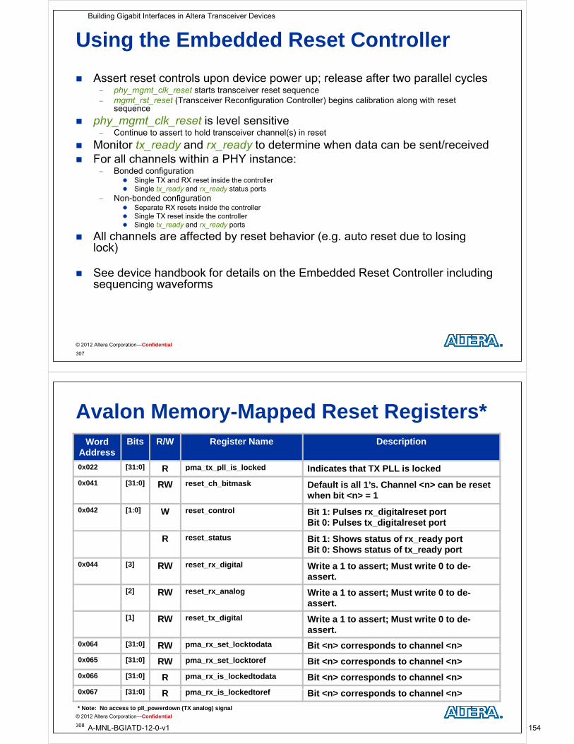
Using the Embedded Reset Controller
Assert reset controls upon device power up; release after two parallel cycles phy_mgmt_clk_reset starts transceiver reset sequence
t t t (T i R fi ti C t ll ) b i lib ti l ith t mgmt_rst_reset (Transceiver Reconfiguration Controller) begins calibration along with reset sequence
phy_mgmt_clk_reset is level sensitive Continue to assert to hold transceiver channel(s) in reset
M it t d d d t d t i h d t b t/ i d Monitor tx_ready and rx_ready to determine when data can be sent/received For all channels within a PHY instance:
Bonded configuration Single TX and RX reset inside the controller Single tx_ready and rx_ready status ports
Non-bonded configuration Separate RX resets inside the controller Single TX reset inside the controller Single tx_ready and rx_ready ports
All channels are affected by reset behavior (e.g. auto reset due to losing lock)
See device handbook for details on the Embedded Reset Controller including See device handbook for details on the Embedded Reset Controller including sequencing waveforms
© 2012 Altera Corporation—Confidential
307
Avalon Memory-Mapped Reset Registers*Word
AddressBits R/W Register Name Description
0x022 [31:0] R pma tx pll is locked Indicates that TX PLL is locked[ ] R pma_tx_pll_is_locked Indicates that TX PLL is locked
0x041 [31:0] RW reset_ch_bitmask Default is all 1’s. Channel <n> can be reset when bit <n> = 1
0x042 [1:0] W reset control Bit 1: Pulses rx digitalreset port[ ] W _ Bit 1: Pulses rx_digitalreset portBit 0: Pulses tx_digitalreset port
R reset_status Bit 1: Shows status of rx_ready portBit 0: Shows status of tx_ready port
0x044 [3] RW reset_rx_digital Write a 1 to assert; Must write 0 to de-assert.
[2] RW reset_rx_analog Write a 1 to assert; Must write 0 to de-assertassert.
[1] RW reset_tx_digital Write a 1 to assert; Must write 0 to de-assert.
0x064 [31:0] RW pma rx set locktodata Bit <n> corresponds to channel <n>0x064 [31:0] RW pma_rx_set_locktodata Bit <n> corresponds to channel <n>
0x065 [31:0] RW pma_rx_set_locktoref Bit <n> corresponds to channel <n>
0x066 [31:0] R pma_rx_is_lockedtodata Bit <n> corresponds to channel <n>
0 067 [31 0] i l k dt f
© 2012 Altera Corporation—Confidential
0x067 [31:0] R pma_rx_is_lockedtoref Bit <n> corresponds to channel <n>
308
* Note: No access to pll_powerdown (TX analog) signal
Building Gigabit Interfaces in Altera Transceiver Devices
A-MNL-BGIATD-12-0-v1 154

Using the Reset Controller IP
Two inputs: clock and reset
Assert reset to asynchronously assert all transceiver PLL, analog and digital reset signalsg g g
reset is level sensitive Continue to assert to hold transceiver channel(s) in reset( )
Monitor tx_ready signal(s) and rx_ready signal(s) to determine when data can be sent/receivedto determine when data can be sent/received
May use PHY management interface signals phy mgmt clk and phy mgmt clk reset for clockphy_mgmt_clk and phy_mgmt_clk_reset for clock and reset
© 2012 Altera Corporation—Confidential
309
Building User-Controlled Reset Logic
Why needed?T ti h i t i t t th t t To tie or synchronize transceiver resets to other system resets
To support specialized protocol reset sequence To design logic that supports resetting an individual channel
Disable Embedded Reset Controller, if available Exposes individual reset ports at top of transceiver instance
D i l i f ll d fi d i Design logic to follow reset sequences defined in device handbook
Assert reset controls upon device power up; release after two Assert reset controls upon device power up; release after two parallel cycles mgmt_rst_reset, pll_powerdown, tx_analogreset, rx_analogreset
Continue to assert digital reset signals until corresponding calibration Continue to assert digital reset signals until corresponding calibration busy flags deasserted tx_digitalreset, rx_digitalreset
© 2012 Altera Corporation—Confidential
310
Building Gigabit Interfaces in Altera Transceiver Devices
A-MNL-BGIATD-12-0-v1 155
Notes on User-Controlled Reset Logic
Reset controller logic must be level sensitive
phy_mgmt_clk_reset does not begin reset sequenceq Must use transceiver reset ports
mgmt rst reset must be asserted to begin g _ _ gcalibration
Use clear text Verilog generated by Reset Use clear text Verilog generated by Reset Controller IP as starting point for custom reset logiclogic
© 2012 Altera Corporation—Confidential
311
Transceiver Design Best Practices
Resource optimization
Planning reset control
Planning transceiver reconfiguration Planning transceiver reconfiguration
PHY IP versions
Pi ti id li Pin connection guidelines
© 2012 Altera Corporation—Confidential
312
Building Gigabit Interfaces in Altera Transceiver Devices
A-MNL-BGIATD-12-0-v1 156
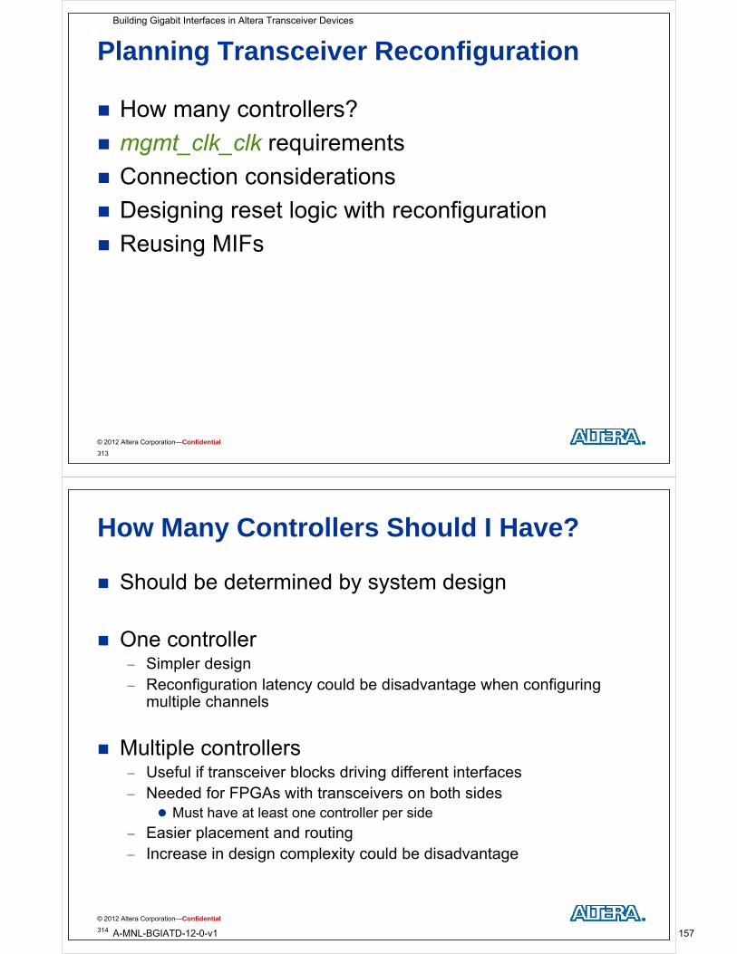
Planning Transceiver Reconfiguration
How many controllers?
mgmt_clk_clk requirements
Connection considerations Connection considerations
Designing reset logic with reconfiguration
R i MIF Reusing MIFs
© 2012 Altera Corporation—Confidential
313
How Many Controllers Should I Have?
Should be determined by system design
One controllerSi l d i Simpler design
Reconfiguration latency could be disadvantage when configuring multiple channels
Multiple controllersUseful if transceiver blocks driving different interfaces Useful if transceiver blocks driving different interfaces
Needed for FPGAs with transceivers on both sides Must have at least one controller per side
E i l t d ti Easier placement and routing Increase in design complexity could be disadvantage
© 2012 Altera Corporation—Confidential
314
Building Gigabit Interfaces in Altera Transceiver Devices
A-MNL-BGIATD-12-0-v1 157
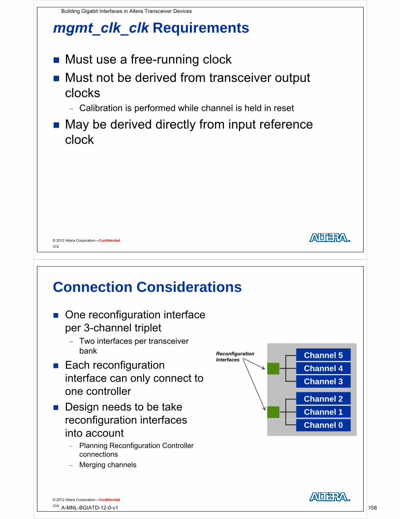
mgmt_clk_clk Requirements
Must use a free-running clock
Must not be derived from transceiver output clocks Calibration is performed while channel is held in reset
May be derived directly from input reference y y pclock
© 2012 Altera Corporation—Confidential
315
Connection Considerations
One reconfiguration interface per 3 channel tripletper 3-channel triplet Two interfaces per transceiver
bank Channel 5Reconfiguration I t f
Each reconfiguration interface can only connect to
t ll
Channel 4
Channel 3
Interfaces
one controller
Design needs to be take reconfiguration interfaces
Channel 2
Channel 1reconfiguration interfaces into account Planning Reconfiguration Controller
Channel 0
connections
Merging channels
© 2012 Altera Corporation—Confidential
316
Building Gigabit Interfaces in Altera Transceiver Devices
A-MNL-BGIATD-12-0-v1 158
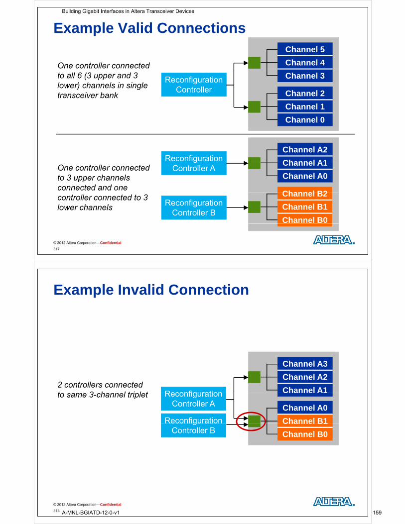
Example Valid ConnectionsChannel 5
Channel 4One controller connected Channel 3
Channel 2
ReconfigurationController
to all 6 (3 upper and 3 lower) channels in single transceiver bank
Channel 1
Channel 0
Channel A2
Channel A1Reconfiguration Channel A1
Channel A0
Channel B2
gController AOne controller connected
to 3 upper channels connected and one
Channel B2
Channel B1
Channel B0
ReconfigurationController B
controller connected to 3 lower channels
© 2012 Altera Corporation—Confidential
317
Example Invalid Connection
Ch l A3Channel A3
Channel A2
Channel A1Reconfiguration2 controllers connected t 3 h l t i l t Channel A1
Channel A0
Channel B1
ReconfigurationController A
Reconfiguration
to same 3-channel triplet
Channel B1
Channel B0
gController B
© 2012 Altera Corporation—Confidential
318
Building Gigabit Interfaces in Altera Transceiver Devices
A-MNL-BGIATD-12-0-v1 159
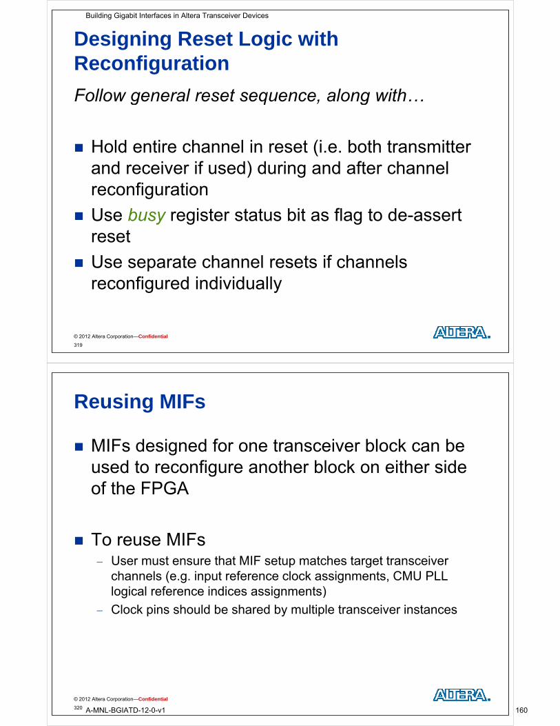
Designing Reset Logic with Reconfiguration
Follow general reset sequence along withFollow general reset sequence, along with…
Hold entire channel in reset (i.e. both transmitter and receiver if used) during and after channel reconfiguration
Use busy register status bit as flag to de-assert y g greset
Use separate channel resets if channelsUse separate channel resets if channels reconfigured individually
© 2012 Altera Corporation—Confidential
319
Reusing MIFs
MIFs designed for one transceiver block can be used to reconfigure another block on either side of the FPGA
To reuse MIFs To reuse MIFs User must ensure that MIF setup matches target transceiver
channels (e.g. input reference clock assignments, CMU PLL l i l f i di i t )logical reference indices assignments)
Clock pins should be shared by multiple transceiver instances
© 2012 Altera Corporation—Confidential
320
Building Gigabit Interfaces in Altera Transceiver Devices
A-MNL-BGIATD-12-0-v1 160
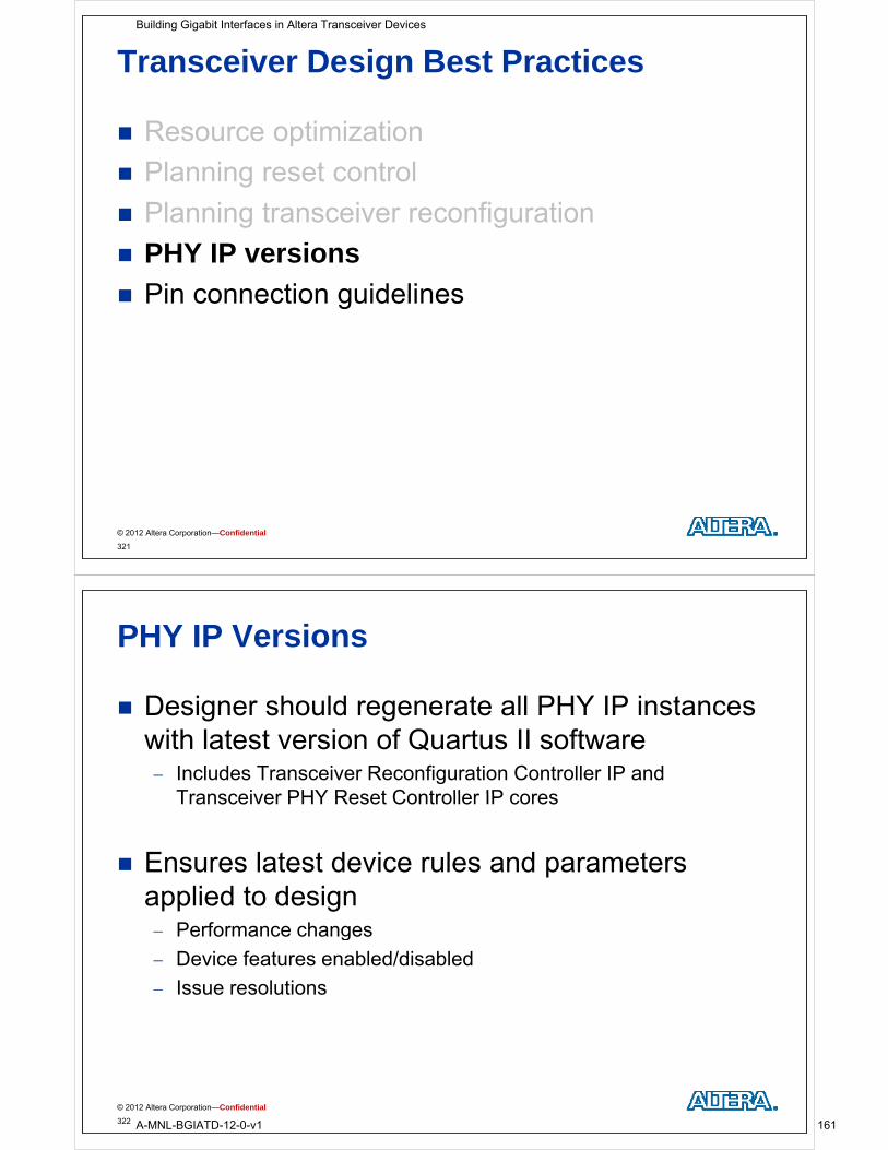
Transceiver Design Best Practices
Resource optimization
Planning reset control
Planning transceiver reconfiguration Planning transceiver reconfiguration
PHY IP versions
Pi ti id li Pin connection guidelines
© 2012 Altera Corporation—Confidential
321
PHY IP Versions
Designer should regenerate all PHY IP instances with latest version of Quartus II software Includes Transceiver Reconfiguration Controller IP and
Transceiver PHY Reset Controller IP coresTransceiver PHY Reset Controller IP cores
Ensures latest device rules and parameters Ensures latest device rules and parameters applied to design
Performance changes Performance changes
Device features enabled/disabled
Issue resolutions
© 2012 Altera Corporation—Confidential
322
Building Gigabit Interfaces in Altera Transceiver Devices
A-MNL-BGIATD-12-0-v1 161
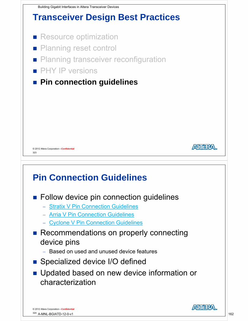
Transceiver Design Best Practices
Resource optimization
Planning reset control
Planning transceiver reconfiguration Planning transceiver reconfiguration
PHY IP versions
Pi ti id li Pin connection guidelines
© 2012 Altera Corporation—Confidential
323
Pin Connection Guidelines
Follow device pin connection guidelines Stratix V Pin Connection Guidelines
Arria V Pin Connection Guidelines
Cyclone V Pin Connection Guidelines Cyclone V Pin Connection Guidelines
Recommendations on properly connecting de ice pinsdevice pins Based on used and unused device features
S i li d d i I/O d fi d Specialized device I/O defined
Updated based on new device information or characterization
© 2012 Altera Corporation—Confidential
324
Building Gigabit Interfaces in Altera Transceiver Devices
A-MNL-BGIATD-12-0-v1 162
Pin Connection Example (RREF Pin)
Connects to device calibration block Calibrates OCT resistors, PLLs and output buffers
Each RREF pin must be connected to GND through an external reference resistor 1.8 kΩ (± 1% tolerance) for Stratix V devices
2 kΩ (± 1% tolerance) for Arria V devices
One per side of FPGA
© 2012 Altera Corporation—Confidential
325
Test Your Knowledge
1. What are the 2 best choices for TX PLLs?
A. ATX PLL and Channel (CMU) PLL
2. How many controllers can connect to a single reconfiguration interface on a triplet?
A. One
3. What is the maximum number of channels that can be bonded when using a CMU PLL? ATX PLL?
A. 4; 6
© 2012 Altera Corporation—Confidential
326
Building Gigabit Interfaces in Altera Transceiver Devices
A-MNL-BGIATD-12-0-v1 163
Please go to Exercise 2g
© 2012 Altera Corporation—Confidential
327
Building Gigabit Interfaces inBuilding Gigabit Interfaces in Altera Transceiver DevicesSSummary
© 2012 Altera Corporation—Confidential
Building Gigabit Interfaces in Altera Transceiver Devices
A-MNL-BGIATD-12-0-v1 164
Summary
Altera 28-nm transceivers support a multitude of high-speed solutions
Follow guidelines and recommendations gpresented in today’s class to have a successful transceiver implementationp
© 2012 Altera Corporation—Confidential
329
References
Stratix V referencesSt ti V D i H db k V l 2 T i Stratix V Device Handbook, Volume 2: Transceivers
Upcoming Stratix V Device Features Stratix V Errata Sheet
Arria V references Arria V Device Handbook, Volume 2: Transceivers
U i A i V D i F t Upcoming Arria V Device Features Arria V Errata Sheet
Cyclone V referencesCyclone V references Cyclone V Device Handbook, Volume 2: Transceivers Upcoming Cyclone V Device Features
E t Sh t Errata Sheet
Altera Transceiver PHY IP Core User Guide
© 2012 Altera Corporation—Confidential
330
Building Gigabit Interfaces in Altera Transceiver Devices
A-MNL-BGIATD-12-0-v1 165
Learn More Through Technical Training
Instructor-Led Online Virtual ClassroomTraining TrainingTraining
With Altera's instructor-led training courses, you can: Learn from an experienced Altera technical
training engineer (instructor)
With Altera's virtual classroom training:Get the best of both worlds!
With Altera's online training courses, you can: Take a course at any time that is training engineer (instructor)
Complete hands-on exercises with guidance from an Altera instructor
Ask questions and receive real-time answers from an Altera instructor
All the benefits of a live, instructor-led training class from the comfort of your home or office
convenient for you
Take a course from the comfort of your home or office (no need to travel as with instructor-led courses)
answers from an Altera instructor
Each instructor-led class is one or two days in length (8 working hours per day)
Each online course takes approximate one to three hours to complete
http://www.altera.com/training
View training class schedule and register for a class
© 2012 Altera Corporation—Confidential
331
g g
Instructor-Led and Virtual Training Curriculum
Quartus IISoftware:
Foundation
Introductionto
VHDL
Quartus IISoftware:
Design Optimization
Quartus II Software:
BestPractices
for
Introduction to
Qsys
Introductionto
Verilog
Software: Timing
Analysis
pUsing
Incremental Compilation
Software:Debus &Analysis
MaximizingFPGA
Productivity(2 days)
Advanced Advanced AdvancedDesigning with the
AdvancedTiming
Timing
Developing
VHDL Verilog Qsys Nios II Processor
TimingAnalysis
Closure
BuildingExternalMemory
Interfaces
VideoDesign
FrameworkWorkshop
Developing SW for
the Nios IIProcessor
(2 days)
DSP Builder
Advanced Blockset
Foundation Classes
Advanced Follow-On Classes
Building Gigabit
Interfaces in Altera
Transceivers
DSP Builder
StandardBlockset
Designing w/ ARM
based SoC
Future Classes
Available as a Virtual Class
System Verilog
Specialized Classes
Scripting ModelSim ® Designing w/ OpenCL
System Console
Partial Reconfiguration
Getting Started w/
PCIe
© 2012 Altera Corporation—Confidential http://www.altera.com/training
Building Gigabit Interfaces in Altera Transceiver Devices
A-MNL-BGIATD-12-0-v1 166
Altera Technical Support
Reference Quartus II software on-line help Quartus II Handbook Quartus II Handbook Consult Altera applications (factory applications engineers)
MySupport: http://www.altera.com/mysupportHotline: (800) 800 EPLD (7:00 a m 5:00 p m PST) Hotline: (800) 800-EPLD (7:00 a.m. - 5:00 p.m. PST)
Field applications engineers: contact your local Altera sales office Altera wiki: http://www.alterawiki.com/ Altera forum: http://www.alteraforum.com/
Discuss issues, ask questions, and share solutions with other Altera users
Receive literature by mail: (888) 3-ALTERAy ( ) FTP: ftp.altera.com World-wide web: http://www.altera.com
Use solutions to search for answers to technical problems Use solutions to search for answers to technical problems View design examples
© 2012 Altera Corporation—Confidential
333
Building Gigabit Interfaces inBuilding Gigabit Interfaces in Altera Transceiver DevicesA diAppendix
© 2012 Altera Corporation—Confidential
Building Gigabit Interfaces in Altera Transceiver Devices
A-MNL-BGIATD-12-0-v1 167
Appendix
Controlling EyeQ
Adaptive Equalization
More on TX PLL Switching More on TX PLL Switching
© 2012 Altera Corporation—Confidential
335
Controlling EyeQ
Register-Based
© 2012 Altera Corporation—Confidential
336
Building Gigabit Interfaces in Altera Transceiver Devices
A-MNL-BGIATD-12-0-v1 168
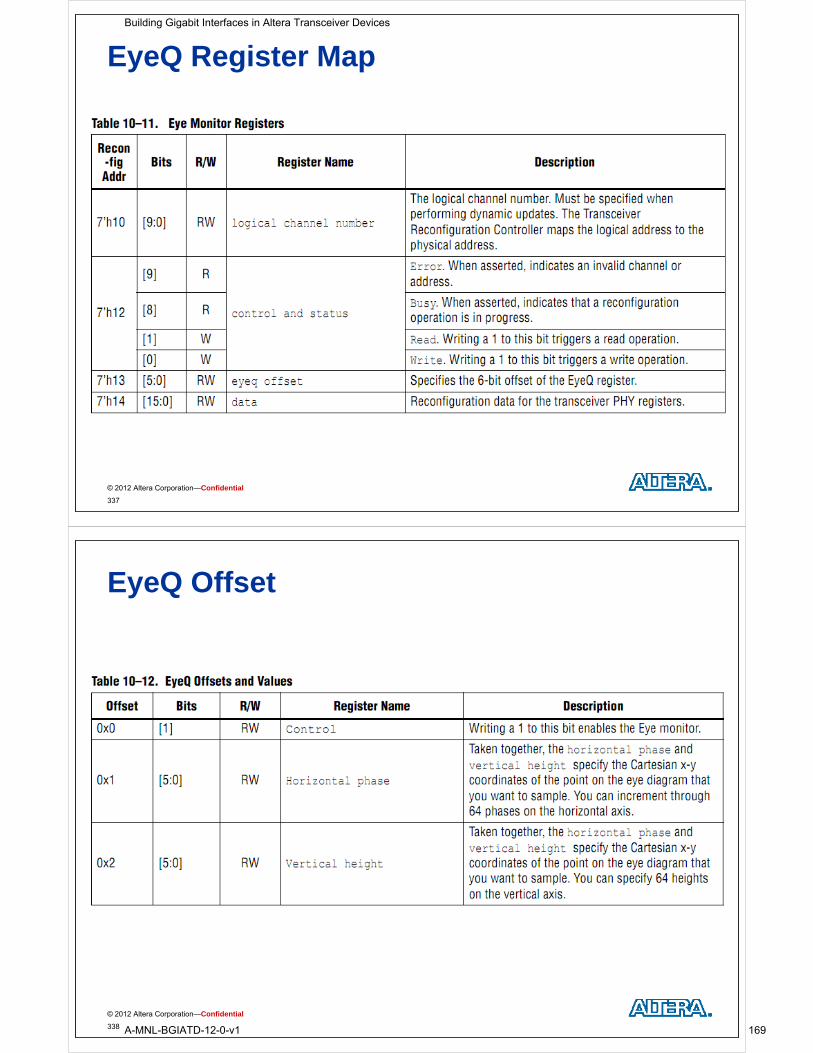
EyeQ Register Map
© 2012 Altera Corporation—Confidential
337
EyeQ Offset
© 2012 Altera Corporation—Confidential
338
Building Gigabit Interfaces in Altera Transceiver Devices
A-MNL-BGIATD-12-0-v1 169
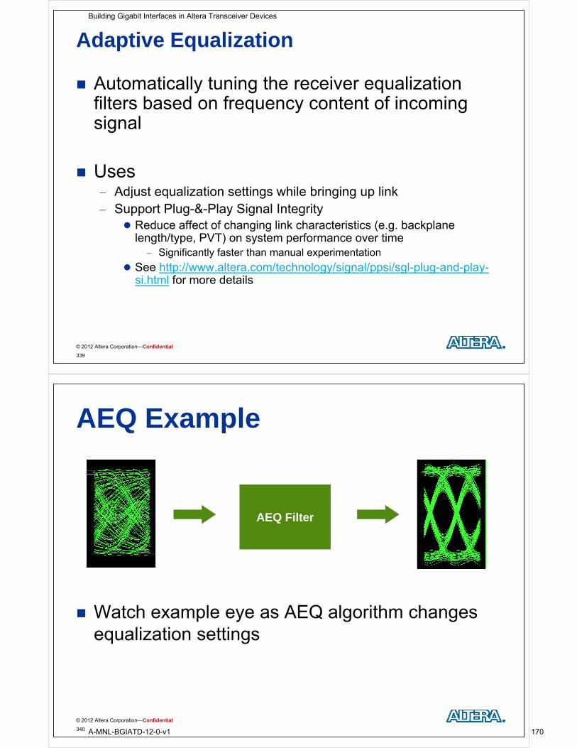
Adaptive Equalization
Automatically tuning the receiver equalization filt b d f t t f i ifilters based on frequency content of incoming signal
UsesAdj t li ti tti hil b i i li k Adjust equalization settings while bringing up link
Support Plug-&-Play Signal Integrity Reduce affect of changing link characteristics (e.g. backplane g g ( g p
length/type, PVT) on system performance over time Significantly faster than manual experimentation
See http://www.altera.com/technology/signal/ppsi/sgl-plug-and-play-fsi.html for more details
© 2012 Altera Corporation—Confidential
339
AEQ ExampleQ p
AEQ FilterAEQ Filter
Watch example eye as AEQ algorithm changes equalization settings
© 2012 Altera Corporation—Confidential
340
Building Gigabit Interfaces in Altera Transceiver Devices
A-MNL-BGIATD-12-0-v1 170
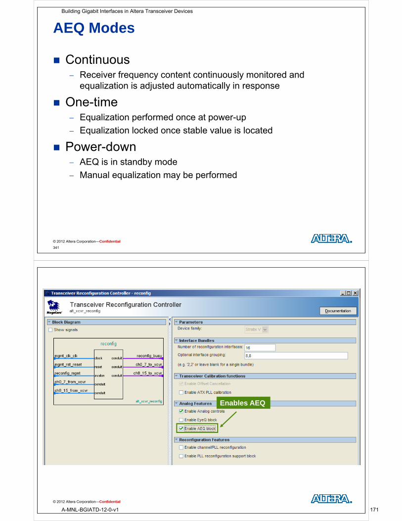
AEQ Modes
Continuous Receiver frequency content continuously monitored and
equalization is adjusted automatically in response
O ti One-time Equalization performed once at power-up
Equalization locked once stable value is located Equalization locked once stable value is located
Power-downAEQ is in standby mode AEQ is in standby mode
Manual equalization may be performed
© 2012 Altera Corporation—Confidential
341
Enables AEQ
© 2012 Altera Corporation—Confidential
Building Gigabit Interfaces in Altera Transceiver Devices
A-MNL-BGIATD-12-0-v1 171
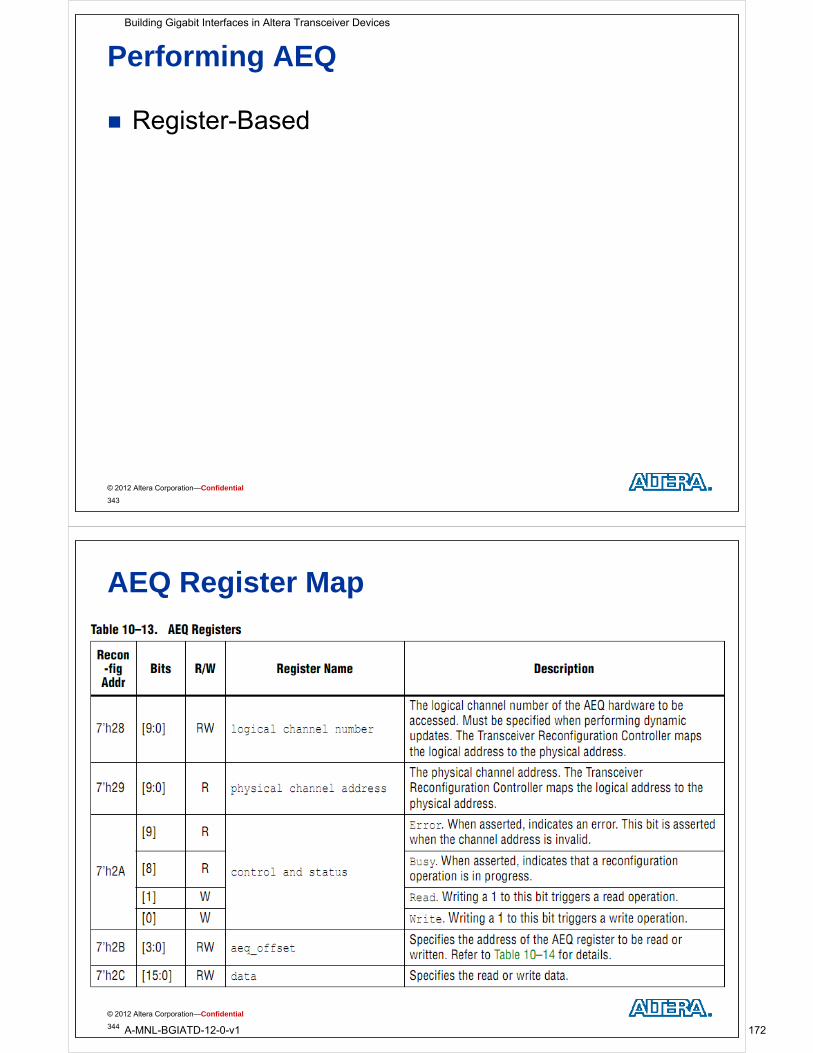
Performing AEQ
Register-Based
© 2012 Altera Corporation—Confidential
343
AEQ Register Map
© 2012 Altera Corporation—Confidential
344
Building Gigabit Interfaces in Altera Transceiver Devices
A-MNL-BGIATD-12-0-v1 172
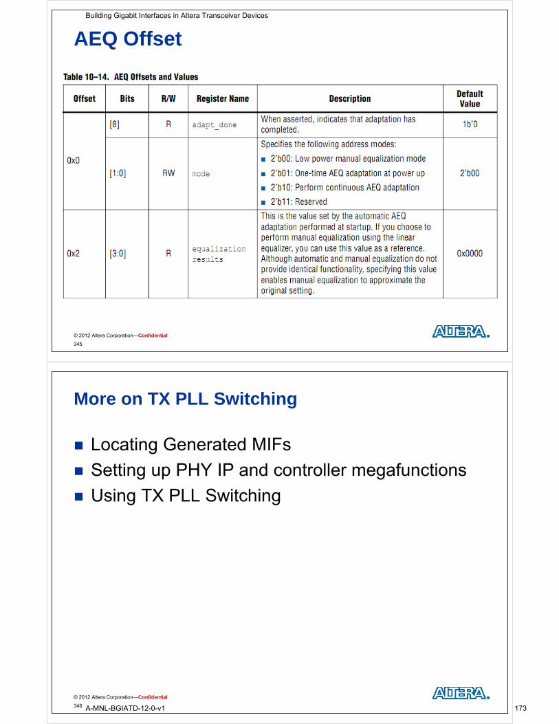
AEQ Offset
© 2012 Altera Corporation—Confidential
345
More on TX PLL Switching
Locating Generated MIFs
Setting up PHY IP and controller megafunctions
Using TX PLL Switching Using TX PLL Switching
© 2012 Altera Corporation—Confidential
346
Building Gigabit Interfaces in Altera Transceiver Devices
A-MNL-BGIATD-12-0-v1 173
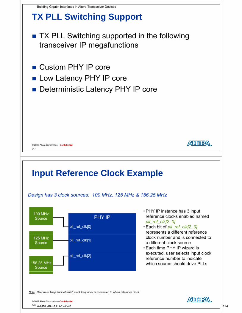
TX PLL Switching Support
TX PLL Switching supported in the following transceiver IP megafunctions
Custom PHY IP core
Low Latency PHY IP core Low Latency PHY IP core
Deterministic Latency PHY IP core
© 2012 Altera Corporation—Confidential
347
Input Reference Clock Example
Design has 3 clock sources: 100 MHz, 125 MHz & 156.25 MHz
PHY IP100 MHz
• PHY IP instance has 3 input reference clocks enabled namedPHY IP
pll_ref_clk[0]
Source reference clocks enabled named pll_ref_clk[2..0]
• Each bit of pll_ref_clk[2..0]represents a different reference
pll_ref_clk[1]125 MHz Source
clock number and is connected to a different clock source
• Each time PHY IP wizard is executed user selects input clock
pll_ref_clk[2]
156.25 MHz Source
executed, user selects input clock reference number to indicate which source should drive PLLs
© 2012 Altera Corporation—Confidential
348
Note: User must keep track of which clock frequency is connected to which reference clock.
Building Gigabit Interfaces in Altera Transceiver Devices
A-MNL-BGIATD-12-0-v1 174
Locating Generated MIFs
reconfig_mif subdirectory created in project directory
Separate MIF created for each transceiver IP pinstance and each TX PLLs referenced in those instances
Default filenames based on the transceiver IP instance namesinstance names User can rename MIF
© 2012 Altera Corporation—Confidential
349
Configuring PHY IP Megafunction
1. Set target data and clock rates (General tab)TX PLL fi d G l f d “ i ” PLL TX PLL configured on General page referred to as “main” PLL
Main PLL will be the driving PLL once configuration is complete
2 Enable Allow PLL Reconfiguration (Reconfiguration tab)2. Enable Allow PLL Reconfiguration (Reconfiguration tab)
3. Specify number of TX PLLs Enables a “TX PLL #” section on the page for each PLLp g
4. Specify number of input reference clocks Or the number of different source clock frequencies being provided to
the PHY IP instancethe PHY IP instance
© 2012 Altera Corporation—Confidential
350
Building Gigabit Interfaces in Altera Transceiver Devices
A-MNL-BGIATD-12-0-v1 175
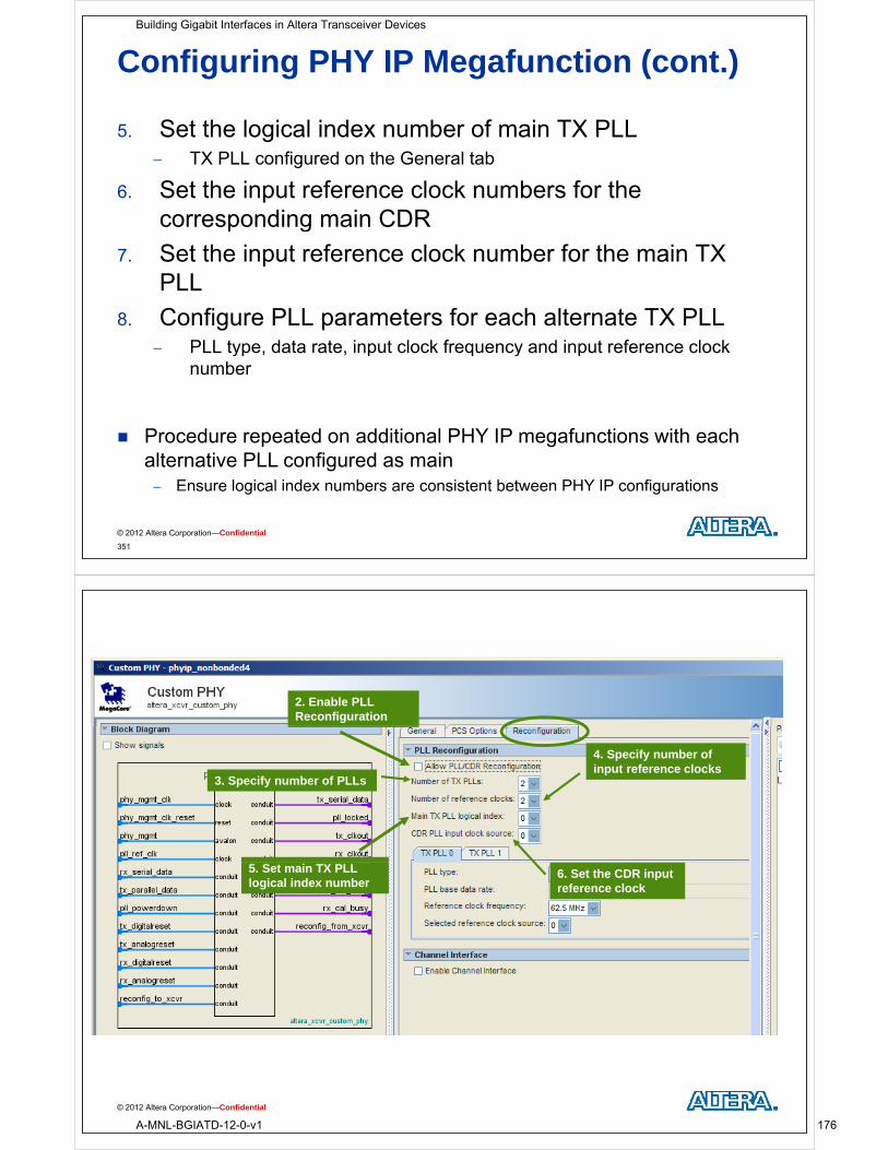
Configuring PHY IP Megafunction (cont.)
5. Set the logical index number of main TX PLLTX PLL fi d h G l b TX PLL configured on the General tab
6. Set the input reference clock numbers for the corresponding main CDRcorresponding main CDR
7. Set the input reference clock number for the main TX PLLPLL
8. Configure PLL parameters for each alternate TX PLL PLL type, data rate, input clock frequency and input reference clock yp , , p q y p
number
Procedure repeated on additional PHY IP megafunctions with each alternative PLL configured as main Ensure logical index numbers are consistent between PHY IP configurations
© 2012 Altera Corporation—Confidential
351
su e og ca de u be s a e co s ste t bet ee co gu at o s
2. Enable PLL Reconfiguration
3. Specify number of PLLs
4. Specify number of input reference clocks
5. Set main TX PLL logical index number
6. Set the CDR input reference clock
© 2012 Altera Corporation—Confidential
Building Gigabit Interfaces in Altera Transceiver Devices
A-MNL-BGIATD-12-0-v1 176
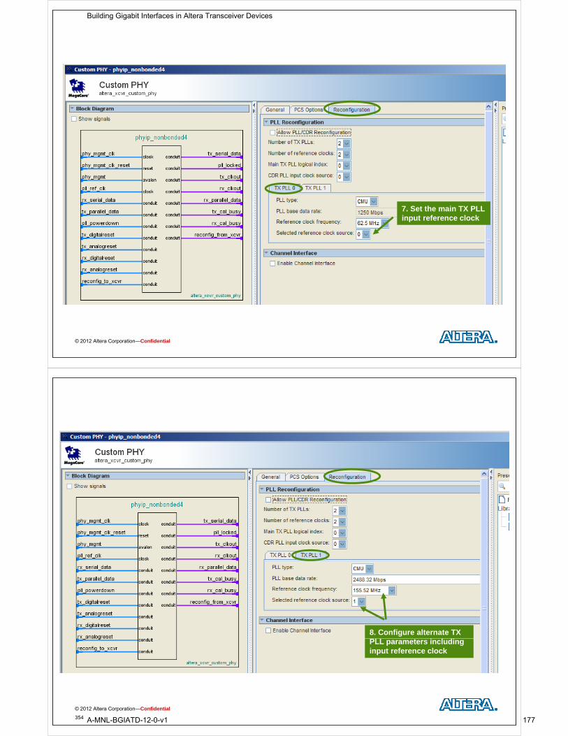
7. Set the main TX PLL input reference clock
© 2012 Altera Corporation—Confidential
8. Configure alternate TX PLL parameters including input reference clock
© 2012 Altera Corporation—Confidential
354
Building Gigabit Interfaces in Altera Transceiver Devices
A-MNL-BGIATD-12-0-v1 177
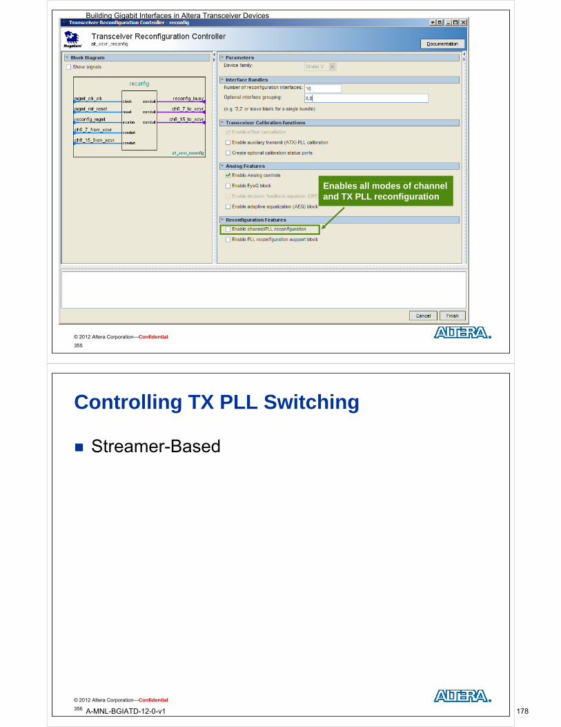
Enables all modes of channel and TX PLL reconfiguration
© 2012 Altera Corporation—Confidential
355
Controlling TX PLL Switching
Streamer-Based
© 2012 Altera Corporation—Confidential
356
Building Gigabit Interfaces in Altera Transceiver Devices
A-MNL-BGIATD-12-0-v1 178
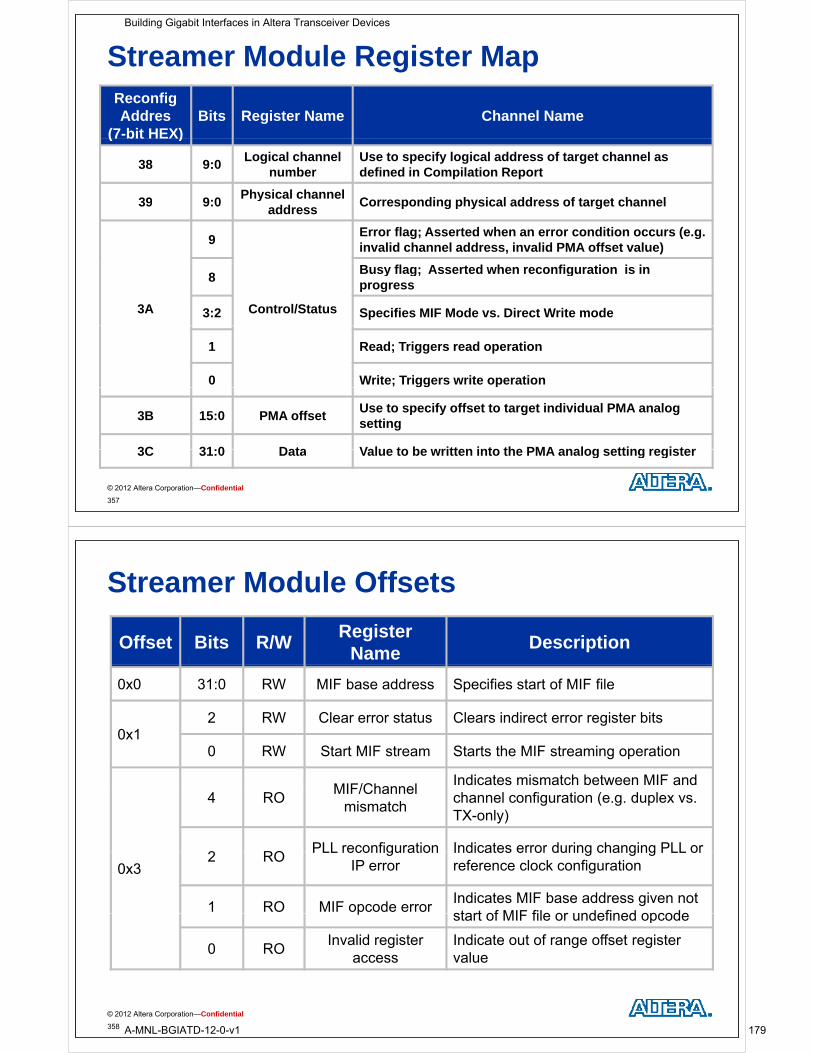
Streamer Module Register MapReconfigAddres
(7-bit HEX)Bits Register Name Channel Name
( )
38 9:0Logical channel
numberUse to specify logical address of target channel as defined in Compilation Report
39 9:0Physical channel
Corresponding physical address of target channel39 9:0y
addressCorresponding physical address of target channel
9Error flag; Asserted when an error condition occurs (e.g. invalid channel address, invalid PMA offset value)
3A Control/Status
8Busy flag; Asserted when reconfiguration is in progress
3:2 Specifies MIF Mode vs. Direct Write mode
1 Read; Triggers read operation
0 Write; Triggers write operation
3B 15:0 PMA offsetUse to specify offset to target individual PMA analog setting
3C 31:0 Data Value to be written into the PMA analog setting register
© 2012 Altera Corporation—Confidential
357
3C 31:0 Data Value to be written into the PMA analog setting register
Streamer Module Offsets
Offset Bits R/WRegister
NameDescription
0x0 31:0 RW MIF base address Specifies start of MIF file
2 RW Clear error status Clears indirect error register bits0x1
0 RW Start MIF stream Starts the MIF streaming operation
MIF/ChannelIndicates mismatch between MIF and
4 ROMIF/Channel
mismatchchannel configuration (e.g. duplex vs. TX-only)
2 ROPLL reconfiguration Indicates error during changing PLL or
0x32 RO
PLL reconfiguration IP error
Indicates error during changing PLL or reference clock configuration
1 RO MIF opcode errorIndicates MIF base address given not start of MIF file or undefined opcode
pstart of MIF file or undefined opcode
0 ROInvalid register
accessIndicate out of range offset register value
© 2012 Altera Corporation—Confidential
358
Building Gigabit Interfaces in Altera Transceiver Devices
A-MNL-BGIATD-12-0-v1 179
Exercise Manual for
Building Gigabit Interfaces in Altera Transceiver Devices
Software requirements to complete all exercises
Software Requirements: Quartus® II software version 12.0
Hardware requirements to complete most exercises
Hardware Requirements: FPGA Development Kit, Stratix® V Edition
Use the link below to download the design files for the exercises:
http://www.altera.com/customertraining/ILT/Building_Gigabit_Interfaces_12_0_v1.zip

Exercises Building Gigabit Interfaces in Altera Transceiver Devices
Copyright © 2012 Altera Corporation A-MNL-BGIATD-EX-12-0-v1
2

Building Gigabit Interfaces in Altera Transceiver Devices Exercises
Copyright © 2012 Altera Corporation A-MNL-BGIATD-EX-12-0-v1
3
Exercise 1
Configuring a Custom PHY IP Core

Exercises Building Gigabit Interfaces in Altera Transceiver Devices
Copyright © 2012 Altera Corporation A-MNL-BGIATD-EX-12-0-v1
4
Building Gigabit Interfaces in Altera Transceiver Devices Exercises
Copyright © 2012 Altera Corporation A-MNL-BGIATD-EX-12-0-v1
5
Exercise 1
Objectives: • Create a transceiver block module with a standard PCS configuration using the
MegaWizard™ Plug-In Manager
• Add the transceiver block module to the partially complete top-level design
• Complete and compile the design in the Quartus II software
Design Details: This simple test design exercises the standard PCS channel to confirm its behavior. It consists of the blocks below:
• The transceiver channel configured as follows:
- Duplex channel with a 32-bit parallel data interface running at 156.25 MHz
- 8B/10B encoding enabled
- Word alignment on K28.5 control characters
• A test driver block that implements a data pattern generator using a state machine that repeatedly generates control characters (idle and alignment) followed by a 32’h00000000, 32’h01010101, 32’h02020202……32’hFFFFFFFF data characters
• A Qsys system that consists of the following control logic:
- JTAG to Avalon® Master bridge to control the PHY by means of JTAG
- Reconfiguration controller as required (discussed later)
- Avalon bridge to connect to the transceiver block outside the Qsys system
• A reset module that ensures proper reset sequence for the transceiver channel
Notes: • Though this design is targeting an Altera® Stratix V GX device, the same steps would
be taken to implement it in any 28-nm device.
Exercises Building Gigabit Interfaces in Altera Transceiver Devices
Copyright © 2012 Altera Corporation A-MNL-BGIATD-EX-12-0-v1
6
Step 1 (Install exercise files)
____ 1. Unzip the lab project files. In an Explorer window, go to C:\altera_trn\Building_Gigabit_Interfaces. This will be your lab installation directory. Delete any old lab file folders that may already exist there labeled XCVR*. Double-click the executable file found in that location. If you still cannot find this file, ask your instructor for assistance. In the WinZip dialog box, simply click Unzip to automatically extract the to the current directory. Close WinZip.
This installs the exercsie files into your local directory underneath a subdirectory named XCVR_12_0. This will be the training directory. Inside the lab files are located in subdirectories Ex1 and Ex2.
Step 2 (Open project and view design)
____ 1. Open the Quartus II software. From the Start menu, select All Programs → Altera → Quartus II 12.0 → Quartus II 12.0.
____ 2. Open the project. From the File menu, choose Open Project. Browse to the the Ex1 folder in the training directory and select the file custom.qpf. Click Open.
____ 3. Open the top-level Verilog file custom.v. In the Project Navigator, double-click on the top-level entity name custom.
You should now be looking at the top-level schematic file. This file instantiates the logic blocks defined above. The only one missing is the transceiver instance. You will create this block in the next step.
Step 3 (Create Stratix V GX transceiver module using MegaWizard Plug-In Manager)
1. Open MegaWizard Plug-In Manger. From the Tools menu of the Quartus II window, select MegaWizard Plug-In Manager…
The window above will appear.
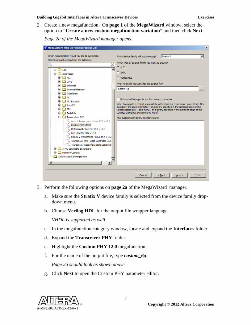
Building Gigabit Interfaces in Altera Transceiver Devices Exercises
Copyright © 2012 Altera Corporation A-MNL-BGIATD-EX-12-0-v1
7
2. Create a new megafunction. On page 1 of the MegaWizard window, select the option to “Create a new custom megafunction variation” and then click Next. Page 2a of the MegaWizard manager opens.
3. Perform the following options on page 2a of the MegaWizard manager.
a. Make sure the Stratix V device family is selected from the device family drop-down menu.
b. Choose Verilog HDL for the output file wrapper language.
VHDL is supported as well.
c. In the megafunction category window, locate and expand the Interfaces folder.
d. Expand the Transceiver PHY folder.
e. Highlight the Custom PHY 12.0 megafunction.
f. For the name of the output file, type custom_6g.
Page 2a should look as shown above.
g. Click Next to open the Custom PHY parameter editor.
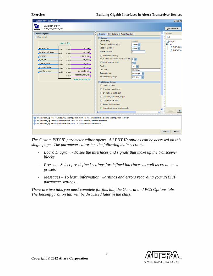
Exercises Building Gigabit Interfaces in Altera Transceiver Devices
Copyright © 2012 Altera Corporation A-MNL-BGIATD-EX-12-0-v1
8
The Custom PHY IP parameter editor opens. All PHY IP options can be accessed on this single page. The parameter editor has the following main sections:
- Board Diagram - To see the interfaces and signals that make up the transceiver blocks
- Presets – Select pre-defined settings for defined interfaces as well as create new presets
- Messages – To learn information, warnings and errors regarding your PHY IP parameter settings.
There are two tabs you must complete for this lab, the General and PCS Options tabs. The Reconfiguration tab will be discussed later in the class.
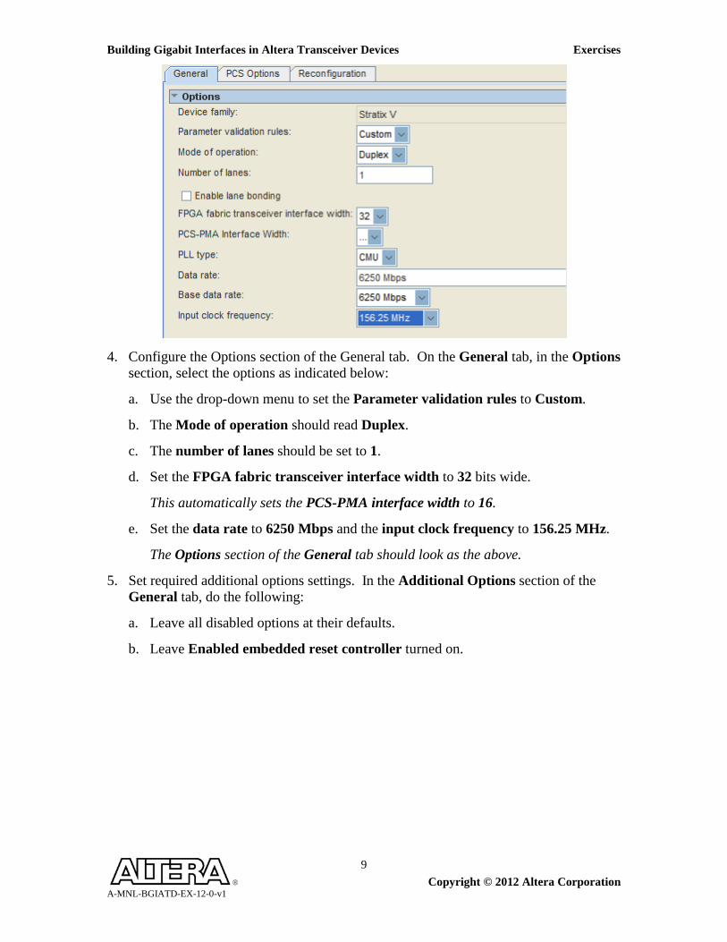
Building Gigabit Interfaces in Altera Transceiver Devices Exercises
Copyright © 2012 Altera Corporation A-MNL-BGIATD-EX-12-0-v1
9
4. Configure the Options section of the General tab. On the General tab, in the Options
section, select the options as indicated below:
a. Use the drop-down menu to set the Parameter validation rules to Custom.
b. The Mode of operation should read Duplex.
c. The number of lanes should be set to 1.
d. Set the FPGA fabric transceiver interface width to 32 bits wide.
This automatically sets the PCS-PMA interface width to 16.
e. Set the data rate to 6250 Mbps and the input clock frequency to 156.25 MHz.
The Options section of the General tab should look as the above.
5. Set required additional options settings. In the Additional Options section of the General tab, do the following:
a. Leave all disabled options at their defaults.
b. Leave Enabled embedded reset controller turned on.
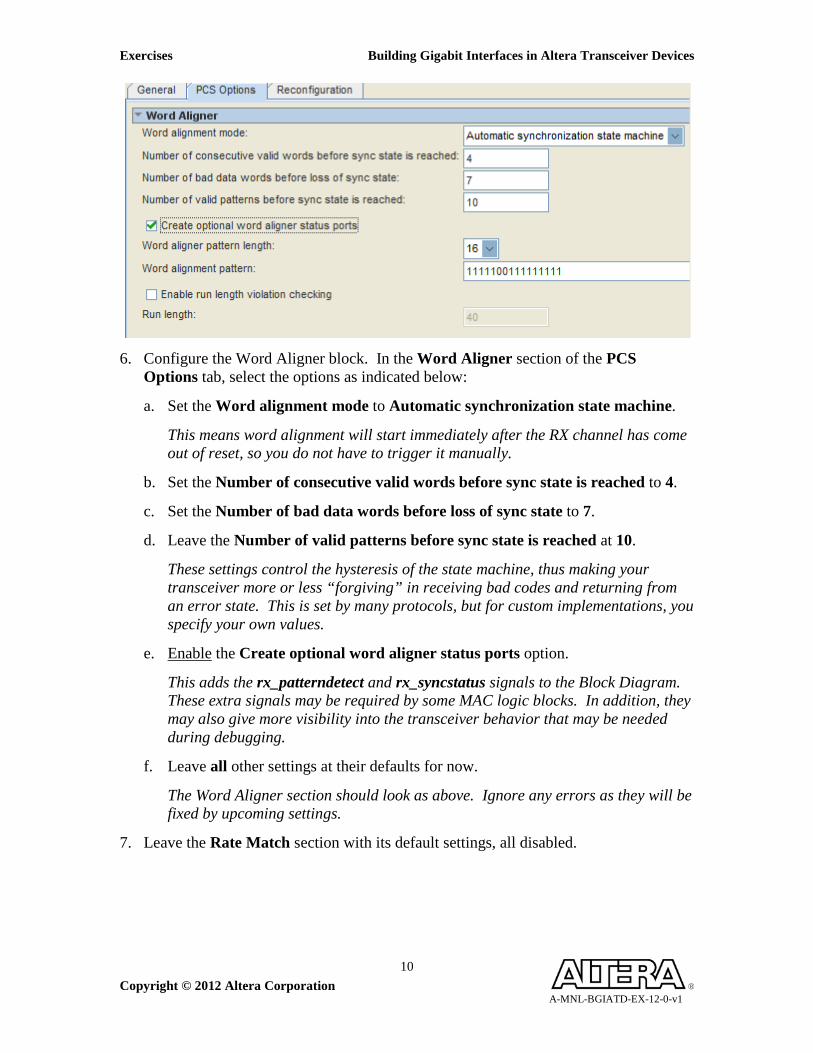
Exercises Building Gigabit Interfaces in Altera Transceiver Devices
Copyright © 2012 Altera Corporation A-MNL-BGIATD-EX-12-0-v1
10
6. Configure the Word Aligner block. In the Word Aligner section of the PCS
Options tab, select the options as indicated below:
a. Set the Word alignment mode to Automatic synchronization state machine.
This means word alignment will start immediately after the RX channel has come out of reset, so you do not have to trigger it manually.
b. Set the Number of consecutive valid words before sync state is reached to 4.
c. Set the Number of bad data words before loss of sync state to 7.
d. Leave the Number of valid patterns before sync state is reached at 10.
These settings control the hysteresis of the state machine, thus making your transceiver more or less “forgiving” in receiving bad codes and returning from an error state. This is set by many protocols, but for custom implementations, you specify your own values.
e. Enable the Create optional word aligner status ports option.
This adds the rx_patterndetect and rx_syncstatus signals to the Block Diagram. These extra signals may be required by some MAC logic blocks. In addition, they may also give more visibility into the transceiver behavior that may be needed during debugging.
f. Leave all other settings at their defaults for now.
The Word Aligner section should look as above. Ignore any errors as they will be fixed by upcoming settings.
7. Leave the Rate Match section with its default settings, all disabled.
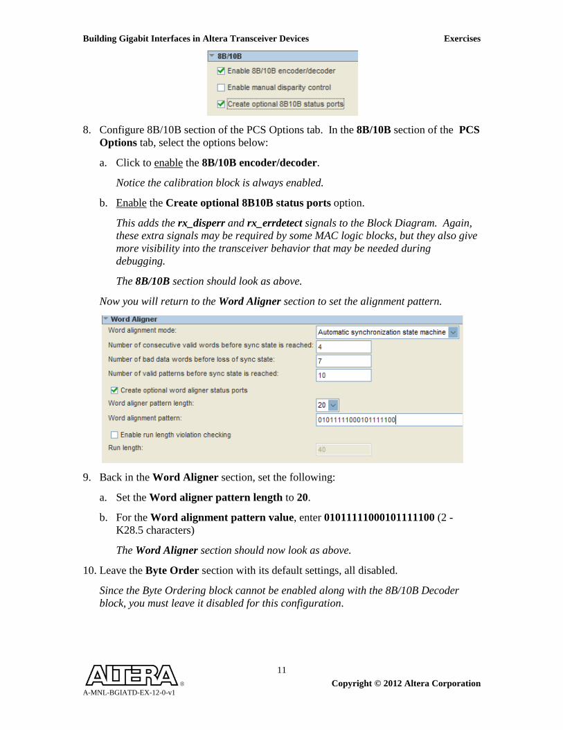
Building Gigabit Interfaces in Altera Transceiver Devices Exercises
Copyright © 2012 Altera Corporation A-MNL-BGIATD-EX-12-0-v1
11
8. Configure 8B/10B section of the PCS Options tab. In the 8B/10B section of the PCS
Options tab, select the options below:
a. Click to enable the 8B/10B encoder/decoder.
Notice the calibration block is always enabled.
b. Enable the Create optional 8B10B status ports option.
This adds the rx_disperr and rx_errdetect signals to the Block Diagram. Again, these extra signals may be required by some MAC logic blocks, but they also give more visibility into the transceiver behavior that may be needed during debugging.
The 8B/10B section should look as above.
Now you will return to the Word Aligner section to set the alignment pattern.
9. Back in the Word Aligner section, set the following:
a. Set the Word aligner pattern length to 20.
b. For the Word alignment pattern value, enter 01011111000101111100 (2 - K28.5 characters)
The Word Aligner section should now look as above.
10. Leave the Byte Order section with its default settings, all disabled.
Since the Byte Ordering block cannot be enabled along with the 8B/10B Decoder block, you must leave it disabled for this configuration.
Exercises Building Gigabit Interfaces in Altera Transceiver Devices
Copyright © 2012 Altera Corporation A-MNL-BGIATD-EX-12-0-v1
12
11. Click Finish.
The parameter editor now runs a script to generate all of the files needed to synthesize and simulate your transceiver implementation.
12. Click Exit when generation is complete.
13. Click Yes to add the Quartus II IP File (.QIP) to the project.
The .QIP file automatically adds all files related to your transceiver instance to the project at once.
You have now created a transceiver channel module custom_6g.v that is configured as required by the design. The next step is to integrate the module in the top-level schematic design file custom.v.
Step 4 (Integrating the Stratix V GX transceiver module in the top-level design)
During this step you would incorporate your transceiver module into the top-level Verilog design file. As this has already been done for you, you will just review the connections to the transceiver block.
1. Locate transceiver instantiation symbol. In the custom.v file, locate the instantiation of the transceiver named custom_6g_inst. Review the port connections.
Looking at the transceiver instantiation, you should first see the PHY management interface connected. This interface is connected to the Qsys control system so that is can be controlled by an Avalon-MM master in that system. You should then see the reference clock and serial input/output channels. Following those are optional status signals that were enabled to monitor the 8B/10B Decoder and Word Aligner. Lastly are the parallel data input and output busses that connect to the pattern generator, or MAC.
Step 5 (Make/check assignments, compile the design and investigate at results)
1. Analyze the design. From the Processing menu, choose Start → Start Analysis & Elaboration. Click OK when complete.
This saves and checks the files and builds a database so you can make assignments.
2. Open and investigate .SDC timing constraint file. From the File menu, select Open. Change Files of type: to Script files (*.tcl, *.sdc, *.qip, *.sip). Choose the file custom.sdc and click Open.
Above are the main contents of the SDC file that you should see. This simple SDC file is being used to constrain most of the transceiver paths and logic. Here you have a create_clock command to define/constrain the input reference clock. Since the input reference clock is also used to drive other logic, the only other clock constraint
create_clock -period 6.4 [get_ports ref_clk_15625] derive_pll_clocks
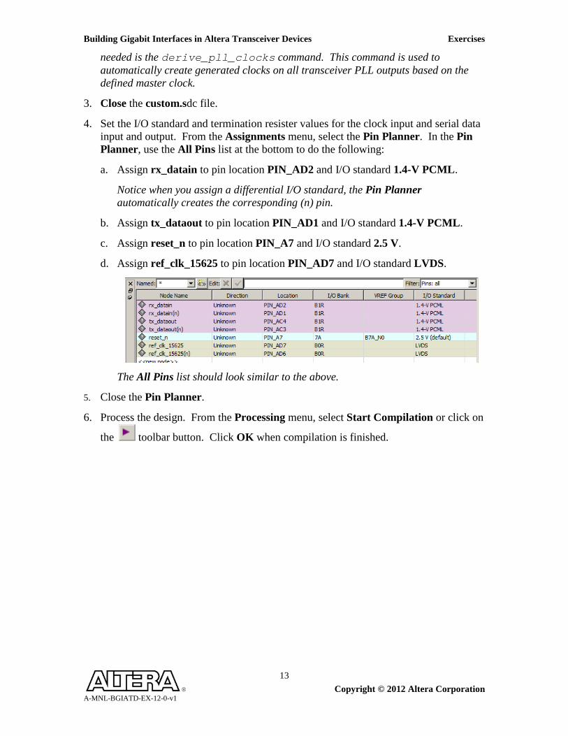
Building Gigabit Interfaces in Altera Transceiver Devices Exercises
Copyright © 2012 Altera Corporation A-MNL-BGIATD-EX-12-0-v1
13
needed is the derive_pll_clocks command. This command is used to automatically create generated clocks on all transceiver PLL outputs based on the defined master clock.
3. Close the custom.sdc file.
4. Set the I/O standard and termination resister values for the clock input and serial data input and output. From the Assignments menu, select the Pin Planner. In the Pin Planner, use the All Pins list at the bottom to do the following:
a. Assign rx_datain to pin location PIN_AD2 and I/O standard 1.4-V PCML.
Notice when you assign a differential I/O standard, the Pin Planner automatically creates the corresponding (n) pin.
b. Assign tx_dataout to pin location PIN_AD1 and I/O standard 1.4-V PCML.
c. Assign reset_n to pin location PIN_A7 and I/O standard 2.5 V.
d. Assign ref_clk_15625 to pin location PIN_AD7 and I/O standard LVDS.
The All Pins list should look similar to the above.
5. Close the Pin Planner.
6. Process the design. From the Processing menu, select Start Compilation or click on
the toolbar button. Click OK when compilation is finished.
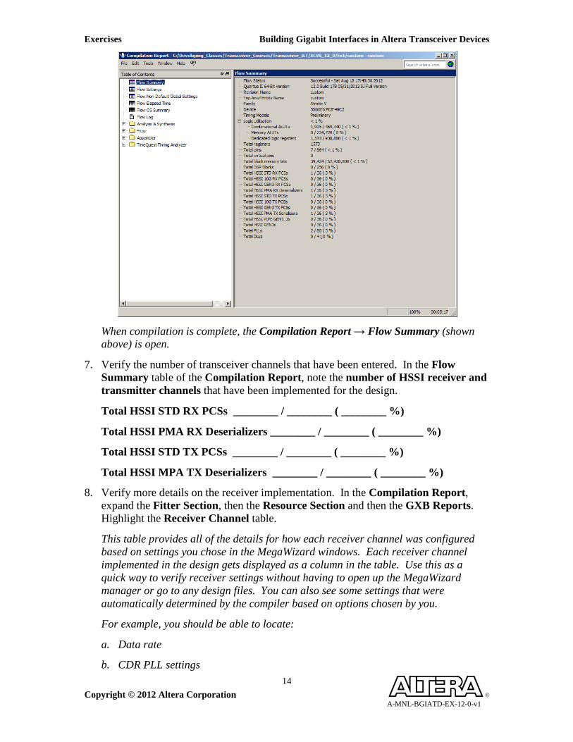
Exercises Building Gigabit Interfaces in Altera Transceiver Devices
Copyright © 2012 Altera Corporation A-MNL-BGIATD-EX-12-0-v1
14
When compilation is complete, the Compilation Report → Flow Summary (shown above) is open.
7. Verify the number of transceiver channels that have been entered. In the Flow Summary table of the Compilation Report, note the number of HSSI receiver and transmitter channels that have been implemented for the design.
Total HSSI STD RX PCSs ________ / ________ ( ________ %)
Total HSSI PMA RX Deserializers ________ / ________ ( ________ %)
Total HSSI STD TX PCSs ________ / ________ ( ________ %)
Total HSSI MPA TX Deserializers ________ / ________ ( ________ %)
8. Verify more details on the receiver implementation. In the Compilation Report, expand the Fitter Section, then the Resource Section and then the GXB Reports. Highlight the Receiver Channel table.
This table provides all of the details for how each receiver channel was configured based on settings you chose in the MegaWizard windows. Each receiver channel implemented in the design gets displayed as a column in the table. Use this as a quick way to verify receiver settings without having to open up the MegaWizard manager or go to any design files. You can also see some settings that were automatically determined by the compiler based on options chosen by you.
For example, you should be able to locate:
a. Data rate
b. CDR PLL settings
Building Gigabit Interfaces in Altera Transceiver Devices Exercises
Copyright © 2012 Altera Corporation A-MNL-BGIATD-EX-12-0-v1
15
c. Location on FPGA
d. Adjustable PMA settings
e. Blocks enabled/disabled and configurations
9. Verify transmitter implementation. In the Compilation Report, underneath the GXB Receiver table, find and highlight the Transmitter Channel table.
Similar to the receiver channel, this table provides all of the configuration information about each transmitter channel implemented in your design.
10. Check TX PLL settings. Highlight the table underneath the Transmitter Channel table, called the Transmitter PLL table.
Since the transmitter PLLs can be shared by multiple transceiver block channels, unlike the receiver PLLs, their information appears in a separate Compilation Report table.
11. Check timing. In the compilation report, expand the TimeQuest Timing Analyzer folder.
Notice that all timing reports (Slow 900mV 85C Model, Slow 900mV 0C Model, Fast 900mV 0C Model) are in black to indicate their timing has passed.
Exercise Summary • Customized a Custom PHY IP core implementation • Incorporated the PHY IP core into a test design and viewed the compilation results
END OF EXERCISE 1

Exercises Building Gigabit Interfaces in Altera Transceiver Devices
Copyright © 2012 Altera Corporation A-MNL-BGIATD-EX-12-0-v1
16
Building Gigabit Interfaces in Altera Transceiver Devices Exercises
Copyright © 2012 Altera Corporation A-MNL-BGIATD-EX-12-0-v1
17
Exercise 2
Implementing Transceiver Design Best Practices

Exercises Building Gigabit Interfaces in Altera Transceiver Devices
Copyright © 2012 Altera Corporation A-MNL-BGIATD-EX-12-0-v1
18

Building Gigabit Interfaces in Altera Transceiver Devices Exercises
Copyright © 2012 Altera Corporation A-MNL-BGIATD-EX-12-0-v1
19
Exercise 2
Objectives:
• Determine and fix placement errors using guidelines and recommendations from Transceiver Design Best Practices section
Design Details: This design implements 3 transceiver PHY IP functions, namely:
• A non-bonded RX-only (x4) interface using the standard PCS and running at 5 Gbps. It is built using the Custom PHY IP core (Cus).
• A bonded TX-only (x4) interface using the 10G PCS and running at 8 Gbps. It is built using the Low-Latency PHY IP core (LL).
• A full duplex (x2) interface using the standard PCS and running at 3.125 Gbps. It uses the Deterministic PHY IP core (Det).
To maximize resource usage, all of these interfaces have been constrained using pin assignments to the same transceiver bank. The assignments are shown below.
Deterministic PHY IP x2
Custom PHY IP x4 (RX only)
Low-Latency PHY IP x4 (TX only)
312.5 MHz ref clock for Deterministic PHY IP
125 MHz ref clock for Custom & Low-Latency PHY IP
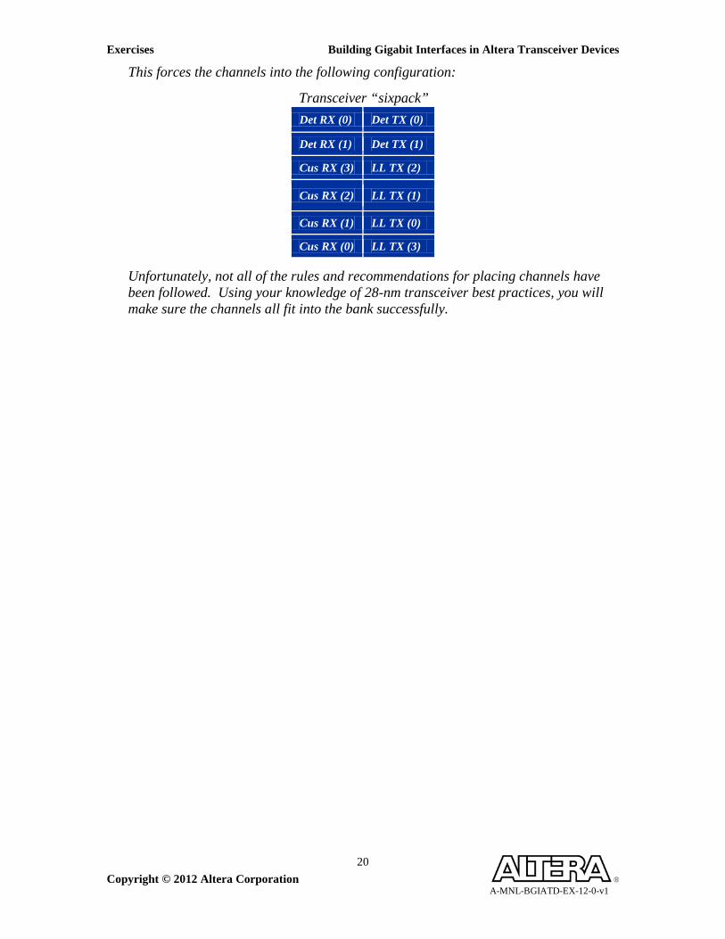
Exercises Building Gigabit Interfaces in Altera Transceiver Devices
Copyright © 2012 Altera Corporation A-MNL-BGIATD-EX-12-0-v1
20
This forces the channels into the following configuration:
Transceiver “sixpack” Det RX (0) Det TX (0)
Det RX (1) Det TX (1)
Cus RX (3) LL TX (2)
Cus RX (2) LL TX (1)
Cus RX (1) LL TX (0)
Cus RX (0) LL TX (3)
Unfortunately, not all of the rules and recommendations for placing channels have been followed. Using your knowledge of 28-nm transceiver best practices, you will make sure the channels all fit into the bank successfully.
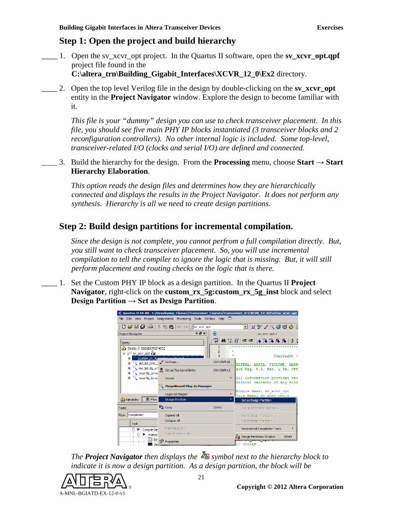
Building Gigabit Interfaces in Altera Transceiver Devices Exercises
Copyright © 2012 Altera Corporation A-MNL-BGIATD-EX-12-0-v1
21
Step 1: Open the project and build hierarchy ____ 1. Open the sv_xcvr_opt project. In the Quartus II software, open the sv_xcvr_opt.qpf
project file found in the C:\altera_trn\Building_Gigabit_Interfaces\XCVR_12_0\Ex2 directory.
____ 2. Open the top level Verilog file in the design by double-clicking on the sv_xcvr_opt entity in the Project Navigator window. Explore the design to become familiar with it.
This file is your “dummy” design you can use to check transceiver placement. In this file, you should see five main PHY IP blocks instantiated (3 transceiver blocks and 2 reconfiguration controllers). No other internal logic is included. Some top-level, transceiver-related I/O (clocks and serial I/O) are defined and connected.
____ 3. Build the hierarchy for the design. From the Processing menu, choose Start → Start Hierarchy Elaboration.
This option reads the design files and determines how they are hierarchically connected and displays the results in the Project Navigator. It does not perform any synthesis. Hierarchy is all we need to create design partitions.
Step 2: Build design partitions for incremental compilation. Since the design is not complete, you cannot perfrom a full compilation directly. But, you still want to check transceiver placement. So, you will use incremental compilation to tell the compiler to ignore the logic that is missing. But, it will still perform placement and routing checks on the logic that is there.
____ 1. Set the Custom PHY IP block as a design partition. In the Quartus II Project Navigator, right-click on the custom_rx_5g:custom_rx_5g_inst block and select Design Partition → Set as Design Partition.
The Project Navigator then displays the symbol next to the hierarchy block to indicate it is now a design partition. As a design partition, the block will be
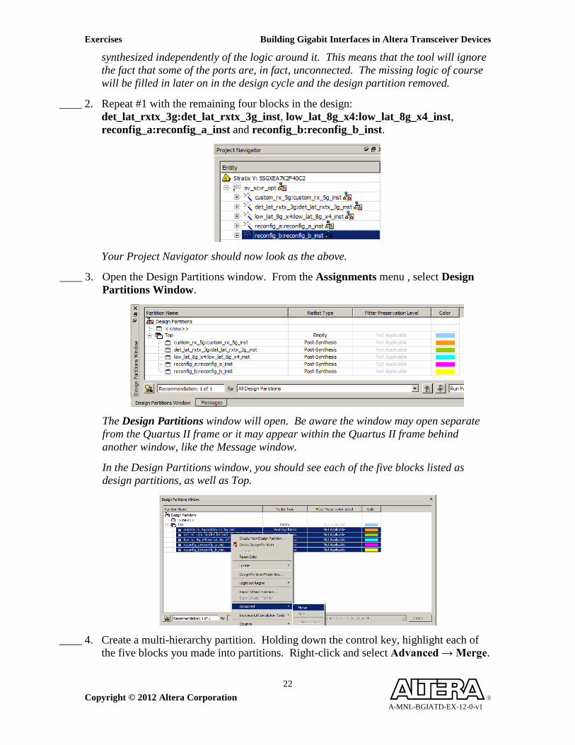
Exercises Building Gigabit Interfaces in Altera Transceiver Devices
Copyright © 2012 Altera Corporation A-MNL-BGIATD-EX-12-0-v1
22
synthesized independently of the logic around it. This means that the tool will ignore the fact that some of the ports are, in fact, unconnected. The missing logic of course will be filled in later on in the design cycle and the design partition removed.
____ 2. Repeat #1 with the remaining four blocks in the design: det_lat_rxtx_3g:det_lat_rxtx_3g_inst, low_lat_8g_x4:low_lat_8g_x4_inst, reconfig_a:reconfig_a_inst and reconfig_b:reconfig_b_inst.
Your Project Navigator should now look as the above.
____ 3. Open the Design Partitions window. From the Assignments menu , select Design Partitions Window.
The Design Partitions window will open. Be aware the window may open separate from the Quartus II frame or it may appear within the Quartus II frame behind another window, like the Message window.
In the Design Partitions window, you should see each of the five blocks listed as design partitions, as well as Top.
____ 4. Create a multi-hierarchy partition. Holding down the control key, highlight each of
the five blocks you made into partitions. Right-click and select Advanced → Merge.
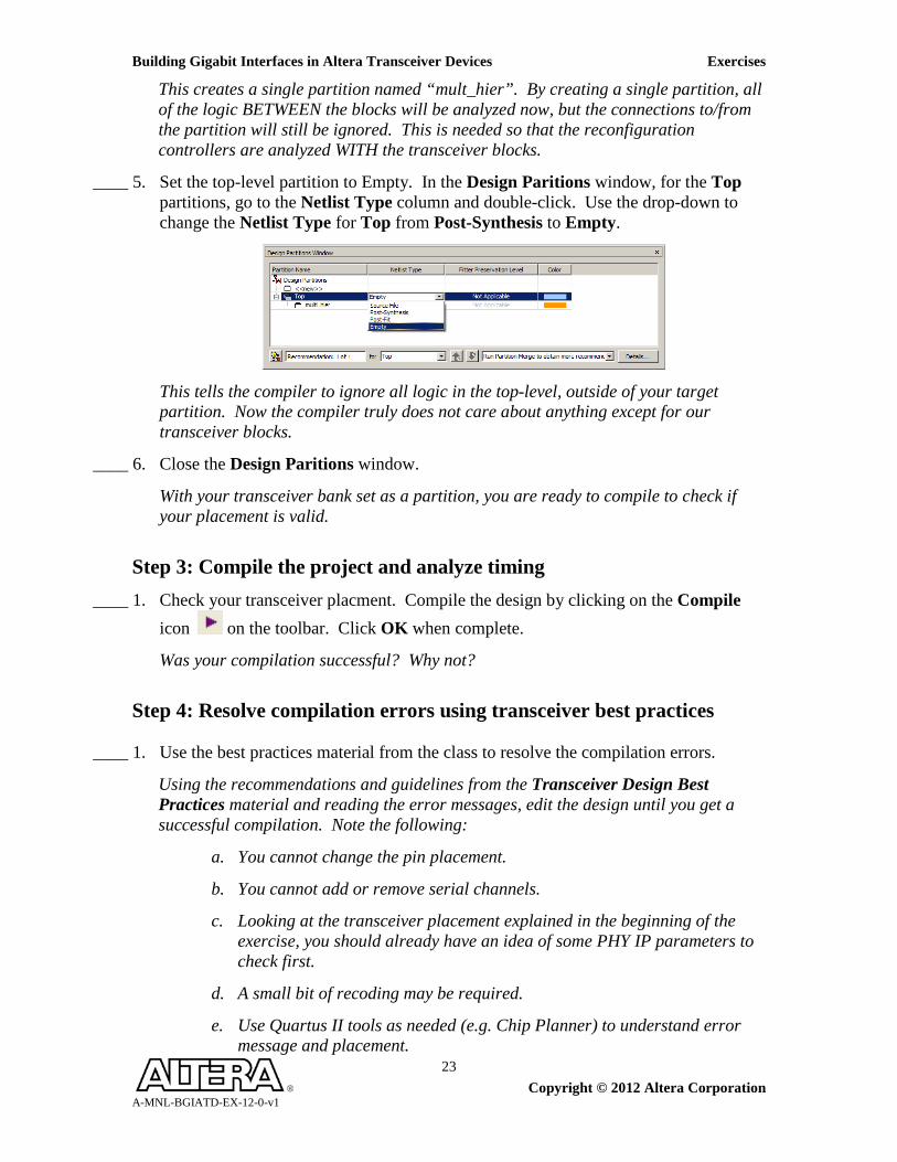
Building Gigabit Interfaces in Altera Transceiver Devices Exercises
Copyright © 2012 Altera Corporation A-MNL-BGIATD-EX-12-0-v1
23
This creates a single partition named “mult_hier”. By creating a single partition, all of the logic BETWEEN the blocks will be analyzed now, but the connections to/from the partition will still be ignored. This is needed so that the reconfiguration controllers are analyzed WITH the transceiver blocks.
____ 5. Set the top-level partition to Empty. In the Design Paritions window, for the Top partitions, go to the Netlist Type column and double-click. Use the drop-down to change the Netlist Type for Top from Post-Synthesis to Empty.
This tells the compiler to ignore all logic in the top-level, outside of your target partition. Now the compiler truly does not care about anything except for our transceiver blocks.
____ 6. Close the Design Paritions window.
With your transceiver bank set as a partition, you are ready to compile to check if your placement is valid.
Step 3: Compile the project and analyze timing ____ 1. Check your transceiver placment. Compile the design by clicking on the Compile
icon on the toolbar. Click OK when complete.
Was your compilation successful? Why not?
Step 4: Resolve compilation errors using transceiver best practices
____ 1. Use the best practices material from the class to resolve the compilation errors.
Using the recommendations and guidelines from the Transceiver Design Best Practices material and reading the error messages, edit the design until you get a successful compilation. Note the following:
a. You cannot change the pin placement.
b. You cannot add or remove serial channels.
c. Looking at the transceiver placement explained in the beginning of the exercise, you should already have an idea of some PHY IP parameters to check first.
d. A small bit of recoding may be required.
e. Use Quartus II tools as needed (e.g. Chip Planner) to understand error message and placement.
Exercises Building Gigabit Interfaces in Altera Transceiver Devices
Copyright © 2012 Altera Corporation A-MNL-BGIATD-EX-12-0-v1
24
Feel free to talk to your instructor if you run into any issues. The Solutions directory contains the finished sv_xcvr_opt.v file which is commented with the changes (look for //*** ***//) f you need further help.
Once you have a successful compilation, you are done. Good job!
Exercise Summary • Use recommendations for transceiver placement to resolve “no fit” issues.
END OF EXERCISE 2