Embed Size (px)
Citation preview
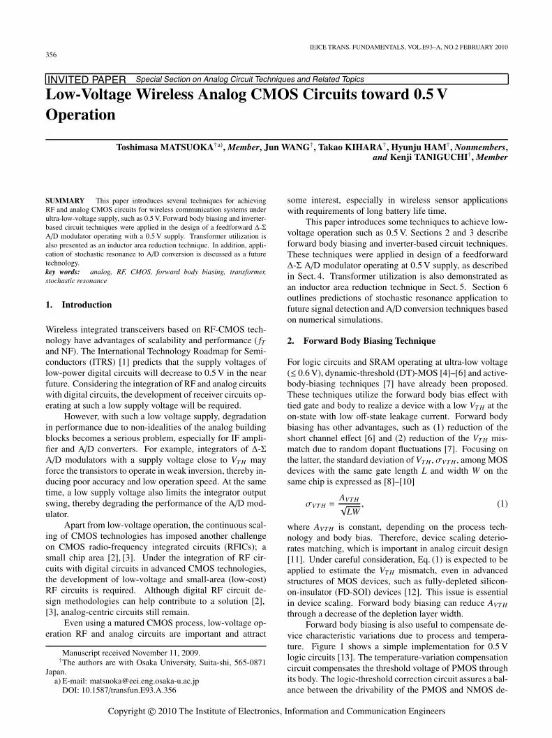
356IEICE TRANS. FUNDAMENTALS, VOL.E93–A, NO.2 FEBRUARY 2010
INVITED PAPER Special Section on Analog Circuit Techniques and Related Topics
Low-Voltage Wireless Analog CMOS Circuits toward 0.5 VOperation
Toshimasa MATSUOKA†a), Member, Jun WANG†, Takao KIHARA†, Hyunju HAM†, Nonmembers,and Kenji TANIGUCHI†, Member
SUMMARY This paper introduces several techniques for achievingRF and analog CMOS circuits for wireless communication systems underultra-low-voltage supply, such as 0.5 V. Forward body biasing and inverter-based circuit techniques were applied in the design of a feedforward Δ-ΣA/D modulator operating with a 0.5 V supply. Transformer utilization isalso presented as an inductor area reduction technique. In addition, appli-cation of stochastic resonance to A/D conversion is discussed as a futuretechnology.key words: analog, RF, CMOS, forward body biasing, transformer,stochastic resonance
1. Introduction
Wireless integrated transceivers based on RF-CMOS tech-nology have advantages of scalability and performance ( fTand NF). The International Technology Roadmap for Semi-conductors (ITRS) [1] predicts that the supply voltages oflow-power digital circuits will decrease to 0.5 V in the nearfuture. Considering the integration of RF and analog circuitswith digital circuits, the development of receiver circuits op-erating at such a low supply voltage will be required.
However, with such a low voltage supply, degradationin performance due to non-idealities of the analog buildingblocks becomes a serious problem, especially for IF ampli-fier and A/D converters. For example, integrators of Δ-ΣA/D modulators with a supply voltage close to VT H mayforce the transistors to operate in weak inversion, thereby in-ducing poor accuracy and low operation speed. At the sametime, a low supply voltage also limits the integrator outputswing, thereby degrading the performance of the A/D mod-ulator.
Apart from low-voltage operation, the continuous scal-ing of CMOS technologies has imposed another challengeon CMOS radio-frequency integrated circuits (RFICs); asmall chip area [2], [3]. Under the integration of RF cir-cuits with digital circuits in advanced CMOS technologies,the development of low-voltage and small-area (low-cost)RF circuits is required. Although digital RF circuit de-sign methodologies can help contribute to a solution [2],[3], analog-centric circuits still remain.
Even using a matured CMOS process, low-voltage op-eration RF and analog circuits are important and attract
Manuscript received November 11, 2009.†The authors are with Osaka University, Suita-shi, 565-0871
Japan.a) E-mail: [email protected]
DOI: 10.1587/transfun.E93.A.356
some interest, especially in wireless sensor applicationswith requirements of long battery life time.
This paper introduces some techniques to achieve low-voltage operation such as 0.5 V. Sections 2 and 3 describeforward body biasing and inverter-based circuit techniques.These techniques were applied in design of a feedforwardΔ-Σ A/D modulator operating at 0.5 V supply, as describedin Sect. 4. Transformer utilization is also demonstrated asan inductor area reduction technique in Sect. 5. Section 6outlines predictions of stochastic resonance application tofuture signal detection and A/D conversion techniques basedon numerical simulations.
2. Forward Body Biasing Technique
For logic circuits and SRAM operating at ultra-low voltage(≤ 0.6 V), dynamic-threshold (DT)-MOS [4]–[6] and active-body-biasing techniques [7] have already been proposed.These techniques utilize the forward body bias effect withtied gate and body to realize a device with a low VT H at theon-state with low off-state leakage current. Forward bodybiasing has other advantages, such as (1) reduction of theshort channel effect [6] and (2) reduction of the VT H mis-match due to random dopant fluctuations [7]. Focusing onthe latter, the standard deviation of VT H , σVT H , among MOSdevices with the same gate length L and width W on thesame chip is expressed as [8]–[10]
σVT H =AVT H√
LW, (1)
where AVT H is constant, depending on the process tech-nology and body bias. Therefore, device scaling deterio-rates matching, which is important in analog circuit design[11]. Under careful consideration, Eq. (1) is expected to beapplied to estimate the VT H mismatch, even in advancedstructures of MOS devices, such as fully-depleted silicon-on-insulator (FD-SOI) devices [12]. This issue is essentialin device scaling. Forward body biasing can reduce AVT H
through a decrease of the depletion layer width.Forward body biasing is also useful to compensate de-
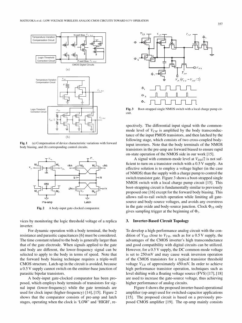
vice characteristic variations due to process and tempera-ture. Figure 1 shows a simple implementation for 0.5 Vlogic circuits [13]. The temperature-variation compensationcircuit compensates the threshold voltage of PMOS throughits body. The logic-threshold correction circuit assures a bal-ance between the drivability of the PMOS and NMOS de-
Copyright c© 2010 The Institute of Electronics, Information and Communication Engineers
MATSUOKA et al.: LOW-VOLTAGE WIRELESS ANALOG CMOS CIRCUITS TOWARD 0.5 V OPERATION357
Fig. 1 (a) Compensation of device characteristic variations with forwardbody biasing, and (b) corresponding control circuits.
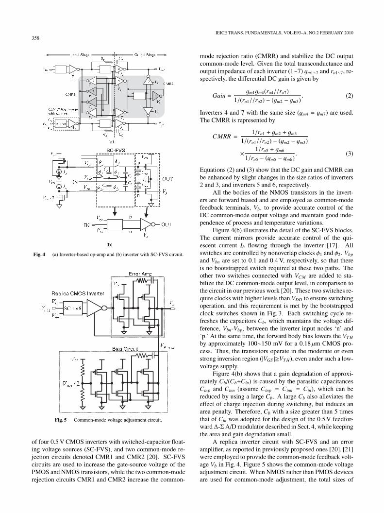
Fig. 2 A body-input gate-clocked comparator.
vices by monitoring the logic threshold voltage of a replicainverter.
For dynamic operation with a body terminal, the bodyresistance and parasitic capacitances [6] must be considered.The time constant related to the body is generally larger thanthat of the gate electrode. When signals applied to the gateand body are different, the lower-frequency signal can beselected to apply to the body in terms of speed. Note thatthe forward body biasing technique requires a triple-wellCMOS structure. Latch-up in the circuit is avoided, becausea 0.5 V supply cannot switch on the emitter-base junction ofparasitic bipolar transistors.
A body-input gate-clocked comparator has been pro-posed, which employs body terminals of transistors for sig-nal input (lower-frequency) while the gate terminals areused for clock input (higher-frequency) [14], [15]. Figure 2shows that the comparator consists of pre-amp and latchstages, operating when the clock is ‘LOW’ and ‘HIGH’, re-
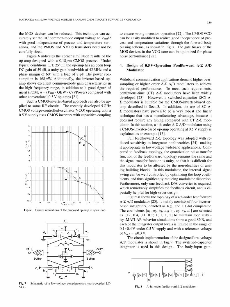
Fig. 3 Boot-strapped single NMOS switch with a local charge pump cir-cuit.
spectively. The differential input signal with the common-mode level of VCM is amplified by the body transconduc-tance of the input PMOS transistors, and then latched by thefollowing stage, which consists of two cross-coupled body-input inverters. Note that the body terminals of the NMOStransistors in the pre-amp are forward biased to ensure rapidon-state operation of the NMOS side in our work [15].
A signal with common-mode level at VDD/2 is not suf-ficient to turn on a transistor switch with a 0.5 V supply. Aneffective solution is to employ a voltage higher (in the caseof NMOS) than the supply with a charge pump to control theswitch transistor gate. Figure 3 shows a boot-strapped singleNMOS switch with a local charge pump circuit [15]. Thisboot-strapping circuit is fundamentally similar to previouslyproposed one [16] except for the forward body biasing. Thisallows rail-to-rail switch operation while limiting all gate-source and body-source voltages, and avoids any overstressin the gate oxide and body-source junction. Clock Φ1S onlygives sampling trigger at the beginning of Φ1.
3. Inverter-Based Circuit Topology
To develop a high-performance analog circuit with the con-dition of VDD close to VT H , such as for a 0.5 V supply, theadvantages of the CMOS inverter’s high transconductanceand good compatibility with digital circuits can be utilized.However, for a 0.5 V supply, the DC common-mode voltageis set to 250 mV and may cause weak inversion operationof the CMOS transistors for a typical transistor thresholdvoltage VT H of approximately 450 mV. In order to achievehigh performance transistor operation, techniques such aslevel shifting with a floating voltage source (FVS) [17], [18]are used to increase the gate-source voltage, thus achievinghigher performance of analog circuits.
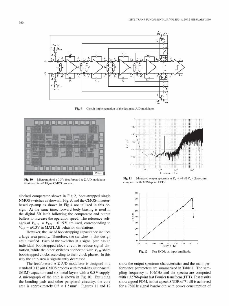
Figure 4 shows the proposed inverter-based operationalamplifier (op-amp) used for switched-capacitor applications[15]. The proposed circuit is based on a previously pro-posed CMOS amplifier [19]. The op-amp mainly consists
358IEICE TRANS. FUNDAMENTALS, VOL.E93–A, NO.2 FEBRUARY 2010
Fig. 4 (a) Inverter-based op-amp and (b) inverter with SC-FVS circuit.
Fig. 5 Common-mode voltage adjustment circuit.
of four 0.5 V CMOS inverters with switched-capacitor float-ing voltage sources (SC-FVS), and two common-mode re-jection circuits denoted CMR1 and CMR2 [20]. SC-FVScircuits are used to increase the gate-source voltage of thePMOS and NMOS transistors, while the two common-moderejection circuits CMR1 and CMR2 increase the common-
mode rejection ratio (CMRR) and stabilize the DC outputcommon-mode level. Given the total transconductance andoutput impedance of each inverter (1∼7) gm1∼7 and ro1∼7, re-spectively, the differential DC gain is given by
Gain =gm1gm4(ro4//ro7)
1/(ro1//ro2) − (gm2 − gm3). (2)
Inverters 4 and 7 with the same size (gm4 = gm7) are used.The CMRR is represented by
CMRR =1/ro1 + gm2 + gm3
1/(ro1//ro2) − (gm2 − gm3)
× 1/ro5 + gm6
1/ro5 − (gm5 − gm6). (3)
Equations (2) and (3) show that the DC gain and CMRR canbe enhanced by slight changes in the size ratios of inverters2 and 3, and inverters 5 and 6, respectively.
All the bodies of the NMOS transistors in the invert-ers are forward biased and are employed as common-modefeedback terminals, Vb, to provide accurate control of theDC common-mode output voltage and maintain good inde-pendence of process and temperature variations.
Figure 4(b) illustrates the detail of the SC-FVS blocks.The current mirrors provide accurate control of the qui-escent current Ib flowing through the inverter [17]. Allswitches are controlled by nonoverlap clocks φ1 and φ2. Vbp
and Vbn are set to 0.1 and 0.4 V, respectively, so that thereis no bootstrapped switch required at these two paths. Theother two switches connected with VCM are added to sta-bilize the DC common-mode output level, in comparison tothe circuit in our previous work [20]. These two switches re-quire clocks with higher levels than VDD to ensure switchingoperation, and this requirement is met by the bootstrappedclock switches shown in Fig. 3. Each switching cycle re-freshes the capacitors Cb, which maintains the voltage dif-ference, Vbn-Vbp, between the inverter input nodes ‘n’ and‘p.’ At the same time, the forward body bias lowers the VT H
by approximately 100∼150 mV for a 0.18 μm CMOS pro-cess. Thus, the transistors operate in the moderate or evenstrong inversion region (|VGS |≥VT H), even under such a low-voltage supply.
Figure 4(b) shows that a gain degradation of approxi-mately Cb/(Cb+Cin) is caused by the parasitic capacitancesCinp and Cinn (assume Cinp = Cinn = Cin), which can bereduced by using a large Cb. A large Cb also alleviates theeffect of charge injection during switching, but induces anarea penalty. Therefore, Cb with a size greater than 5 timesthat of Cin was adopted for the design of the 0.5 V feedfor-ward Δ-ΣA/D modulator described in Sect. 4, while keepingthe area and gain degradation small.
A replica inverter circuit with SC-FVS and an erroramplifier, as reported in previously proposed ones [20], [21]were employed to provide the common-mode feedback volt-age Vb in Fig. 4. Figure 5 shows the common-mode voltageadjustment circuit. When NMOS rather than PMOS devicesare used for common-mode adjustment, the total sizes of
MATSUOKA et al.: LOW-VOLTAGE WIRELESS ANALOG CMOS CIRCUITS TOWARD 0.5 V OPERATION359
the MOS devices can be reduced. This technique can ac-curately set the DC common-mode output voltage to VDD/2with good independence of process and temperature vari-ations, and the PMOS and NMOS transistors need not becarefully sized.
Figure 6 indicates the corner simulation results of theop-amp designed with a 0.18 μm CMOS process. Undertypical conditions (TT, 25◦C), the op-amp has an open loopDC gain of 59 dB, a unity gain bandwidth of 42 MHz and aphase margin of 60◦ with a load of 8 pF. The power con-sumption is 168 μW. Additionally, the inverter-based op-amp shows excellent common-mode gain characteristics inthe high frequency range, in addition to a good figure ofmerit (FOM; η = (VDD · GBW · CL)/Power) compared withother conventional 0.5 V op-amps [21].
Such a CMOS-inverter-based approach can also be ap-plied to some RF circuits. The recently developed 5 GHzCMOS voltage-controlled-oscillator(VCO) operating with a0.5 V supply uses CMOS inverters with capacitive coupling
Fig. 6 Corner simulations of the proposed op-amp in open loop.
Fig. 7 Schematic of a low-voltage complementary cross-coupled LC-VCO.
to ensure strong inversion operation [22]. The CMOS VCOcan be easily modified to realize good independece of pro-cess and temperature variations through the forward bodybiasing scheme, as shown in Fig. 7. The gate biases of theMOS devices in the VCO core can be optimized for phasenoise performance [22].
4. Design of 0.5 V-Operation Feedforward Δ-Σ A/DModulator
Wideband communication applications demand higher over-sampling or higher order Δ-Σ A/D modulators to achievethe required performance. To meet such requirements,continuous-time (CT) Δ-Σ modulators have been widelydeveloped [23]. However, a switched-capacitor (SC) Δ-Σ modulator is suitable for the CMOS-inverter-based op-amp described in Sect. 3. In addition, the use of SC Δ-Σ modulators have proven to be a very robust and lineartechnique that has a manufacturing advantage, because itdoes not require any tuning compared with CT Δ-Σ mod-ulator. In this section, a 4th-order Δ-Σ A/D modulator usinga CMOS-inverter-based op-amp operating at 0.5 V supply isexplained as an example [15].
Full feedforward Δ-Σ topology was adopted with re-duced sensitivity to integrator nonlinearities [24], makingit appropriate in low-voltage wideband applications. Com-pared to feedback topology, the quantization noise transferfunction of the feedforward topology remains the same andthe signal transfer function is unity, so that it is difficult forthis modulator to be affected by the non-idealities of ana-log building blocks. In this modulator, the internal signalswing can be well controlled by optimizing the loop coeffi-cients, and thus significantly reducing modulator distortion.Furthermore, only one feedback D/A converter is required,which remarkably simplifies the feedback circuit, and is es-pecially helpful for high-order design.
Figure 8 shows the topology of a 4th-order feedforwardΔ-Σ A/D modulator [25]. It mainly consists of four inverter-based integrators, denoted as I(z), and a 1-bit comparator.The coefficients [a1, a2, a3, a4; c1, c2, c3, c4] are selectedas [0.2, 0.4, 0.1, 0.1; 1, 1, 1, 2] to maintain loop stabil-ity. MATLAB behavior simulations show a good SNR, andeach of the integrator output levels is limited in the range of0.1∼0.4 V under 0.5 V supply and with a reference voltageof Vre f = ±0.3 V.
The circuit implementation of the designed low-voltageA/D modulator is shown in Fig. 9. The switched-capacitorintegrator is used in this design. The body-input gate-
Fig. 8 A 4th-order feedforward Δ-Σ modulator.
360IEICE TRANS. FUNDAMENTALS, VOL.E93–A, NO.2 FEBRUARY 2010
Fig. 9 Circuit implementation of the designed A/D modulator.
Fig. 10 Micrograph of a 0.5 V feedforward Δ-Σ A/D modulatorfabricated in a 0.18 μm CMOS process.
clocked comparator shown in Fig. 2, boot-strapped singleNMOS switches as shown in Fig. 3, and the CMOS-inverter-based op-amp as shown in Fig. 4 are utilized in this de-sign. At the same time, forward body biasing is used inthe digital SR latch following the comparator and outputbuffers to increase the operation speed. The reference volt-ages of Vre f± = VCM ± 0.15 V are used, corresponding toVre f = ±0.3V in MATLAB behavior simulations.
However, the use of bootstrapping capacitance inducesa large area penalty. Therefore, the switches in this designare classified. Each of the switches at a signal path has anindividual bootstrapped clock circuit to reduce signal dis-tortion, while the other switches connected with VCM sharebootstrapped clocks according to their clock phases. In thisway the chip area is significantly decreased.
The feedforward Δ-Σ A/D modulator is designed in astandard 0.18 μm CMOS process with metal-insulator-metal(MIM) capacitors and six metal layers with a 0.5 V supply.A micrograph of the chip is shown in Fig. 10. Excludingthe bonding pads and other peripheral circuitry, the corearea is approximately 0.5 × 1.5 mm2. Figures 11 and 12
Fig. 11 Measured output spectrum at Vin = −8 dBVre f (Spectrumcomputed with 32768-point FFT).
Fig. 12 Test SNDR vs. input amplitude.
show the output spectrum characteristics and the main per-formance parameters are summarized in Table 1. The sam-pling frequency is 10 MHz and the spectra are computedwith a 32768-point fast Fourier transform (FFT). Test resultsshow a good FOM, in that a peak SNDR of 71 dB is achievedfor a 78 kHz signal bandwidth with power consumption of
MATSUOKA et al.: LOW-VOLTAGE WIRELESS ANALOG CMOS CIRCUITS TOWARD 0.5 V OPERATION361
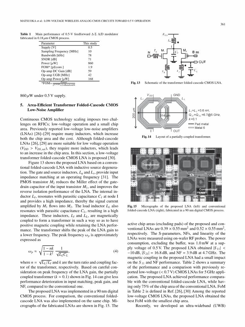
Table 1 Main performance of 0.5-V feedforward Δ-Σ A/D modulatorfabricated in 0.18 μm CMOS process.
Parameter This studySupply [V] 0.5Sampling Frequency [MHz] 10Bandwidth [kHz] 78SNDR [dB] 71Power [μW] 860FOM* [pJ/conv.] 1.9Op-amp DC Gain [dB] 59Op-amp UGB [MHz] 42Op-amp Power [μW] 168*FOM= Power
2ENOB×2×Bandwidth
860 μW under 0.5 V supply.
5. Area-Efficient Transformer Folded-Cascode CMOSLow-Noise Amplifier
Continuous CMOS technology scaling imposes two chal-lenges on RFICs; low-voltage operation and a small chiparea. Previously reported low-voltage low-noise amplifiers(LNAs) [26]–[29] require many inductors, which increaseboth the chip area and the cost. Although folded-cascodeLNAs [26], [29] are more suitable for low voltage operation(VDD > VDS ,sat), they require more inductors, which leadsto an increase in the chip area. In this section, a low-voltagetransformer folded-cascode CMOS LNA is proposed [30].
Figure 13 shows the proposed LNA based on a conven-tional folded-cascode LNA with inductive source degenera-tion. The gate and source inductors, Lg and Ls, provide inputimpedance matching at an operating frequency [31]. ThePMOS transistor M2 reduces the Miller effect of the gate-drain capacitor of the input transistor M1, and improves thereverse isolation performance of the LNA. The internal in-ductor LI , resonates with parasitic capacitance CI at node Iand provides a high impedance, thereby the signal currentamplified by M1 flows into M2. The load inductor LL alsoresonates with parasitic capacitance CL, resulting in a highimpedance. These inductors, LI and LL, are magneticallycoupled to form a transformer in such a way so as to havepositive magnetic coupling while retaining the LNA perfor-mance. The transformer shifts the peak of the LNA gain toa lower frequency. The peak frequency ωp is approximatelyexpressed as
ωp ≈√
1 − nk1 − k2
1√LLCL
, (4)
where n =√
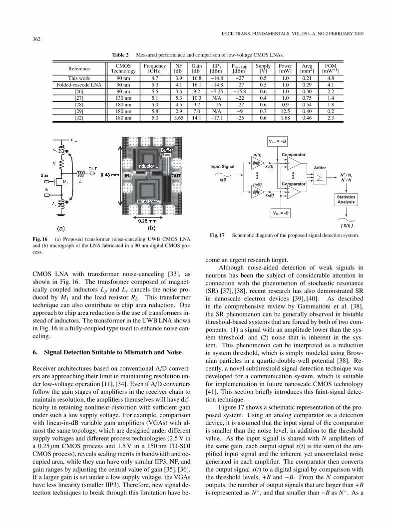
LL/LI and k are the turn ratio and coupling fac-tor of the transformer, respectively. Based on careful con-sideration on peak frequency of the LNA gain, the partiallycoupled transformer (k 0.1) shown in Fig. 14 can give lessperformance deterioration in input matching, peak gain, andNF, compared to the conventional one.
The proposed LNA was implemented in a 90 nm digitalCMOS process. For comparison, the conventional folded-cascode LNA was also implemented on the same chip. Mi-crographs of the fabricated LNAs are shown in Fig. 15. The
Fig. 13 Schematic of the transformer folded-cascode CMOS LNA.
Fig. 14 Layout of a partially-coupled transformer.
Fig. 15 Micrographs of the proposed LNA (left) and conventionalfolded-cascode LNA (right), fabricated in a 90 nm digital CMOS process.
active chip areas (excluding pads) of the proposed and con-ventional LNAs are 0.39 × 0.55 mm2 and 0.52 × 0.55 mm2,respectively. The S-parameters, NFs, and linearity of theLNAs were measured using on-wafer RF probes. The powerconsumption, excluding the buffer, was 1.0 mW at a sup-ply voltage of 0.5 V. The proposed LNA obtained |S 11| <−10 dB, |S 21| = 16.8 dB, and NF = 3.9 dB at 4.7 GHz. Themagnetic coupling in the proposed LNA had a small impacton the S 11 and NF performance. Table 2 shows a summaryof the performance and a comparison with previously re-ported low-voltage (< 0.7 V) CMOS LNAs for 5 GHz appli-cation. The proposed LNA achieved performance compara-ble with the conventional folded-cascode LNA, while hav-ing only 75% of the chip area of the conventional LNA. FoMin Table 2 is defined in Ref. [26], [30] Among the reportedlow-voltage CMOS LNAs, the proposed LNA obtained thebest FoM with the smallest chip area.
Recently, we developed an ultra-wideband (UWB)
362IEICE TRANS. FUNDAMENTALS, VOL.E93–A, NO.2 FEBRUARY 2010
Table 2 Measured performance and comparison of low-voltage CMOS LNAs.
Reference CMOS Frequency NF Gain IIP3 Pin−1 dB Supply Power Area FOMTechnology [GHz] [dB] [dB] [dBm] [dBm] [V] [mW] [mm2] [mW−1]
This work 90 nm 4.7 3.9 16.8 −14.8 −27 0.5 1.0 0.21 4.8Folded-cascode LNA 90 nm 5.0 4.1 16.1 −14.8 −27 0.5 1.0 0.29 4.1
[26] 90 nm 5.5 3.6 9.2 −7.25 −15.8 0.6 1.0 0.30 2.2[27] 130 nm 5.1 5.3 10.3 N/A −22 0.4 1.0 0.75 1.4[28] 180 nm 5.0 4.5 9.2 −16 −27 0.6 0.9 0.54 1.8[29] 180 nm 5.8 2.9 7.0 N/A −9 0.7 12.5 0.40 0.2[32] 180 nm 5.0 3.65 14.1 −17.1 −25 0.6 1.68 0.46 2.3
Fig. 16 (a) Proposed transformer noise-canceling UWB CMOS LNAand (b) micrograph of the LNA fabricated in a 90 nm digital CMOS pro-cess.
CMOS LNA with transformer noise-canceling [33], asshown in Fig. 16. The transformer composed of magnet-ically coupled inductors Lp and Ls cancels the noise pro-duced by M1 and the load resistor RL. This transformertechnique can also contribute to chip area reduction. Oneapproach to chip area reduction is the use of transformers in-stead of inductors. The transformer in the UWB LNA shownin Fig. 16 is a fully-coupled type used to enhance noise can-celing.
6. Signal Detection Suitable to Mismatch and Noise
Receiver architectures based on conventional A/D convert-ers are approaching their limit in maintaining resolution un-der low-voltage operation [11], [34]. Even if A/D convertersfollow the gain stages of amplifiers in the receiver chain tomaintain resolution, the amplifiers themselves will have dif-ficulty in retaining nonlinear-distortion with sufficient gainunder such a low supply voltage. For example, comparisonwith linear-in-dB variable gain amplifiers (VGAs) with al-most the same topology, which are designed under differentsupply voltages and different process technologies (2.5 V ina 0.25 μm CMOS process and 1.5 V in a 150 nm FD-SOICMOS process), reveals scaling merits in bandwidth and oc-cupied area, while they can have only similar IIP3, NF, andgain ranges by adjusting the central value of gain [35], [36].If a larger gain is set under a low supply voltage, the VGAshave less linearity (smaller IIP3). Therefore, new signal de-tection techniques to break through this limitation have be-
Fig. 17 Schematic diagram of the proposed signal detection system.
come an urgent research target.Although noise-aided detection of weak signals in
neurons has been the subject of considerable attention inconnection with the phenomenon of stochastic resonance(SR) [37], [38], recent research has also demonstrated SRin nanoscale electron devices [39], [40]. As describedin the comprehensive review by Gammaitoni et al. [38],the SR phenomenon can be generally observed in bistablethreshold-based systems that are forced by both of two com-ponents: (1) a signal with an amplitude lower than the sys-tem threshold, and (2) noise that is inherent in the sys-tem. This phenomenon can be interpreted as a reductionin system threshold, which is simply modeled using Brow-nian particles in a quartic-double-well potential [38]. Re-cently, a novel subthreshold signal detection technique wasdeveloped for a communication system, which is suitablefor implementation in future nanoscale CMOS technology[41]. This section briefly introduces this faint-signal detec-tion technique.
Figure 17 shows a schematic representation of the pro-posed system. Using an analog comparator as a detectiondevice, it is assumed that the input signal of the comparatoris smaller than the noise level, in addition to the thresholdvalue. As the input signal is shared with N amplifiers ofthe same gain, each output signal x(t) is the sum of the am-plified input signal and the inherent yet uncorrelated noisegenerated in each amplifier. The comparator then convertsthe output signal x(t) to a digital signal by comparison withthe threshold levels, +B and −B. From the N comparatoroutputs, the number of output signals that are larger than +Bis represented as N+, and that smaller than −B as N−. As a
MATSUOKA et al.: LOW-VOLTAGE WIRELESS ANALOG CMOS CIRCUITS TOWARD 0.5 V OPERATION363
result, two output values, N+ and N−, are obtained from oneinput signal s(t).
Note that the thermal and shot noise in electrical de-vices are represented as typical Gaussian white noise [42].Under such Gaussian white noise, the input signal s(t) canbe restored from the probability for detection of a signal us-ing the time or ensemble statistics of the comparator outputs,that is, N+/N and N−/N, as follows.
S (i) =
⎧⎪⎪⎪⎪⎪⎪⎪⎪⎪⎪⎪⎪⎪⎪⎪⎪⎪⎪⎪⎨⎪⎪⎪⎪⎪⎪⎪⎪⎪⎪⎪⎪⎪⎪⎪⎪⎪⎪⎪⎩
B − √2σn erf −1
{2
(12− N+
N
)}
(N+i > N−i ),
−B − √2σn erf −1
{2
(N−
N− 1
2
)}
(N+i < N−i ),
0 (N+i = N−i ).
(5)
Here σn is the standard deviation of the noise, and S (i) rep-resents the sample value of s(t) at t = i Ts (i = 0, 1, 2, · · ·),where Ts is the sampling period.
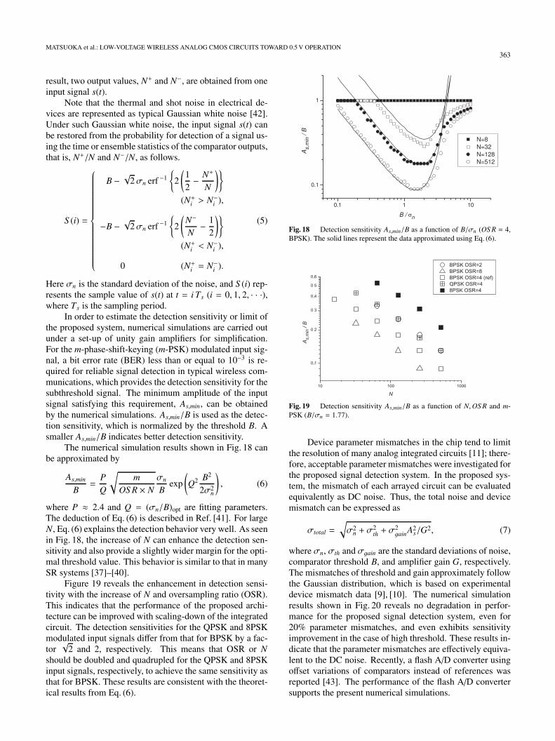
In order to estimate the detection sensitivity or limit ofthe proposed system, numerical simulations are carried outunder a set-up of unity gain amplifiers for simplification.For the m-phase-shift-keying (m-PSK) modulated input sig-nal, a bit error rate (BER) less than or equal to 10−3 is re-quired for reliable signal detection in typical wireless com-munications, which provides the detection sensitivity for thesubthreshold signal. The minimum amplitude of the inputsignal satisfying this requirement, As,min, can be obtainedby the numerical simulations. As,min/B is used as the detec-tion sensitivity, which is normalized by the threshold B. Asmaller As,min/B indicates better detection sensitivity.
The numerical simulation results shown in Fig. 18 canbe approximated by
As,min
B=
PQ
√m
OS R × Nσn
Bexp
(Q2 B2
2σ2n
), (6)
where P ≈ 2.4 and Q = (σn/B)opt are fitting parameters.The deduction of Eq. (6) is described in Ref. [41]. For largeN, Eq. (6) explains the detection behavior very well. As seenin Fig. 18, the increase of N can enhance the detection sen-sitivity and also provide a slightly wider margin for the opti-mal threshold value. This behavior is similar to that in manySR systems [37]–[40].
Figure 19 reveals the enhancement in detection sensi-tivity with the increase of N and oversampling ratio (OSR).This indicates that the performance of the proposed archi-tecture can be improved with scaling-down of the integratedcircuit. The detection sensitivities for the QPSK and 8PSKmodulated input signals differ from that for BPSK by a fac-tor√
2 and 2, respectively. This means that OSR or Nshould be doubled and quadrupled for the QPSK and 8PSKinput signals, respectively, to achieve the same sensitivity asthat for BPSK. These results are consistent with the theoret-ical results from Eq. (6).
Fig. 18 Detection sensitivity As,min/B as a function of B/σn (OS R = 4,BPSK). The solid lines represent the data approximated using Eq. (6).
Fig. 19 Detection sensitivity As,min/B as a function of N,OS R and m-PSK (B/σn = 1.77).
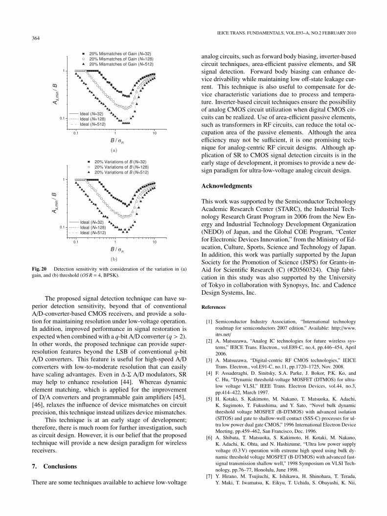
Device parameter mismatches in the chip tend to limitthe resolution of many analog integrated circuits [11]; there-fore, acceptable parameter mismatches were investigated forthe proposed signal detection system. In the proposed sys-tem, the mismatch of each arrayed circuit can be evaluatedequivalently as DC noise. Thus, the total noise and devicemismatch can be expressed as
σtotal =
√σ2
n + σ2th + σ
2gainA2
s/G2, (7)
where σn, σth and σgain are the standard deviations of noise,comparator threshold B, and amplifier gain G, respectively.The mismatches of threshold and gain approximately followthe Gaussian distribution, which is based on experimentaldevice mismatch data [9], [10]. The numerical simulationresults shown in Fig. 20 reveals no degradation in perfor-mance for the proposed signal detection system, even for20% parameter mismatches, and even exhibits sensitivityimprovement in the case of high threshold. These results in-dicate that the parameter mismatches are effectively equiva-lent to the DC noise. Recently, a flash A/D converter usingoffset variations of comparators instead of references wasreported [43]. The performance of the flash A/D convertersupports the present numerical simulations.
364IEICE TRANS. FUNDAMENTALS, VOL.E93–A, NO.2 FEBRUARY 2010
Fig. 20 Detection sensitivity with consideration of the variation in (a)gain, and (b) threshold (OS R = 4, BPSK).
The proposed signal detection technique can have su-perior detection sensitivity, beyond that of conventionalA/D-converter-based CMOS receivers, and provide a solu-tion for maintaining resolution under low-voltage operation.In addition, improved performance in signal restoration isexpected when combined with a q-bit A/D converter (q > 2).In other words, the proposed technique can provide super-resolution features beyond the LSB of conventional q-bitA/D converters. This feature is useful for high-speed A/Dconverters with low-to-moderate resolution that can easilyhave scaling advantages. Even in Δ-Σ A/D modulators, SRmay help to enhance resolution [44]. Whereas dynamicelement matching, which is applied for the improvementof D/A converters and programmable gain amplifiers [45],[46], relaxes the influence of device mismatches on circuitprecision, this technique instead utilizes device mismatches.
This technique is at an early stage of development;therefore, there is much room for further investigation, suchas circuit design. However, it is our belief that the proposedtechnique will provide a new design paradigm for wirelessreceivers.
7. Conclusions
There are some techniques available to achieve low-voltage
analog circuits, such as forward body biasing, inverter-basedcircuit techniques, area-efficient passive elements, and SRsignal detection. Forward body biasing can enhance de-vice drivability while maintaining low off-state leakage cur-rent. This technique is also useful to compensate for de-vice characteristic variations due to process and tempera-ture. Inverter-based circuit techniques ensure the possibilityof analog CMOS circuit utilization when digital CMOS cir-cuits can be realized. Use of area-efficient passive elements,such as transformers in RF circuits, can reduce the total oc-cupation area of the passive elements. Although the areaefficiency may not be sufficient, it is one promising tech-nique for analog-centric RF circuit designs. Although ap-plication of SR to CMOS signal detection circuits is in theearly stage of development, it promises to provide a new de-sign paradigm for ultra-low-voltage analog circuit design.
Acknowledgments
This work was supported by the Semiconductor TechnologyAcademic Research Center (STARC), the Industrial Tech-nology Research Grant Program in 2006 from the New En-ergy and Industrial Technology Development Organization(NEDO) of Japan, and the Global COE Program, “Centerfor Electronic Devices Innovation,” from the Ministry of Ed-ucation, Culture, Sports, Science and Technology of Japan.In addition, this work was partially supported by the JapanSociety for the Promotion of Science (JSPS) for Grants-in-Aid for Scientific Research (C) (#20560324). Chip fabri-cation in this study was also supported by the Universityof Tokyo in collaboration with Synopsys, Inc. and CadenceDesign Systems, Inc.
References
[1] Semiconductor Industry Association, “International technologyroadmap for semiconductors 2007 edition.” Available: http://www.itrs.net/
[2] A. Matsuzawa, “Analog IC technologies for future wireless sys-tems,” IEICE Trans. Electron., vol.E89-C, no.4, pp.446–454, April2006.
[3] A. Matsuzawa, “Digital-centric RF CMOS technologies,” IEICETrans. Electron., vol.E91-C, no.11, pp.1720–1725, Nov. 2008.
[4] F. Assaderaghi, D. Sinitsky, S.A. Parke, J. Bokor, P.K. Ko, andC. Hu, “Dynamic threshold-voltage MOSFET (DTMOS) for ultra-low voltage VLSI,” IEEE Trans. Electron Devices, vol.44, no.3,pp.414–422, March 1997.
[5] H. Kotaki, S. Kakimoto, M. Nakano, T. Matsuoka, K. Adachi,K. Sugimoto, T. Fukushima, and Y. Sato, “Novel bulk dynamicthreshold voltage MOSFET (B-DTMOS) with advanced isolation(SITOS) and gate to shallow-well contact (SSS-C) processes for ul-tra low power dual gate CMOS,” 1996 International Electron DeviceMeeting, pp.459–462, San Francisco, Dec. 1996.
[6] A. Shibata, T. Matsuoka, S. Kakimoto, H. Kotaki, M. Nakano,K. Adachi, K. Ohta, and N. Hashizume, “Ultra low power supplyvoltage (0.3 V) operation with extreme high speed using bulk dy-namic threshold voltage MOSFET (B-DTMOS) with advanced fast-signal transmission shallow well,” 1998 Symposium on VLSI Tech-nology, pp.76–77, Honolulu, June 1998.
[7] Y. Hirano, M. Tsujiuchi, K. Ishikawa, H. Shinohara, T. Terada,Y. Maki, T. Iwamatsu, K. Eikyu, T. Uchida, S. Obayashi, K. Nii,
MATSUOKA et al.: LOW-VOLTAGE WIRELESS ANALOG CMOS CIRCUITS TOWARD 0.5 V OPERATION365
Y. Tsukamoto, M. Yabuuchi, T. Ipposhi, H. Oda, and Y. Inoue, “A ro-bust silicon-on-insulator static-random-access-memory architectureby using advanced actively body-bias controlled technology,” Jpn. J.Appl. Phys., vol.47, no.4, pp.2092–2096, April 2008.
[8] M.J.M. Pelgrom, A.C.J. Duinmaijer, and A.P.G. Welbers, “Matchingproperties of MOS transistors,” IEEE J. Solid-State Circuits, vol.24,no.5, pp.1433–1440, Oct. 1989.
[9] Y. Shimizu, M. Nakamura, T. Matsuoka, and K. Taniguchi, “Teststructure for precise measurement of MOSFET matching proper-ties,” IEICE Trans. Electron (Japanese Edition), vol.J86-C, no.7,pp.726–733, July 2003.
[10] Y. Shimizu, M. Nakamura, T. Matsuoka, and K. Taniguchi, “Teststructure for precise measurement of MOSFET matching proper-ties,” Electron. Commun. Jpn 2, Electron, vol.87, no.3, pp.21–28,2004.
[11] K. Uyttenhove and M.S.J. Steyaert, “Speed-power-accuracy tradeoffin high-speed CMOS ADCs,” IEEE Trans. Circuits Syst. II, vol.49,no.4, pp.280–287, April 2002.
[12] Y. Shimizu, T. Matsuoka, and K. Taniguchi, “Threshold voltage mis-match of FD-SOI MOSFETs,” IEICE Trans. Electron., vol.E87-C,no.6, pp.1013–1014, June 2004.
[13] K. Yasue, J. Wang, T. Matsuoka, and K. Taniguchi, “Characteristicscompensation of ultra-low-voltage CMOS digital circuits,” IEICETrans. Electron. (Japanese Edition), vol.J93-C, no.2, pp.75–77, Feb.2010.
[14] K.P. Pun, S. Chatterjee, and P. Kinget, “A 0.5-V 74-dB SNDR25-kHz continuous-time Delta-Sigma modulator with a return-to-open DAC,” IEEE J. Solid-State Circuits, vol.42, no.3, pp.496–507,March 2007.
[15] J. Wang, T. Matsuoka, and K. Taniguchi, “A 0.5 V feedforwarddelta-sigma modulator with inverter-based integrator,” 35th Euro-pean Solid-State Circuits Conference, pp.328–331, Athens, Sept.2009.
[16] M. Dessouky and A. Kaiser, “Input switch configuration suitable forrail-to-rail operation of switched-opamp circuits,” Electron. Lett.,vol.35, no.1, pp.8–10, Jan. 1999.
[17] F. Munoz, A. Torralba, R.G. Carvaja, and J. Ramirez-Angulo, “Twonew VHF tunable CMOS low-voltage linear transconductors andtheir application to HF GM-C filter design,” Proc. IEEE Int. Symp.Circuits and Systems, Geneva, vol.V, pp.173–176, May 2000.
[18] R.G. Carvajal, A. Torralba, J. Ramirez-Angulo, J. Tombs, and F.Munoz, “Low voltage class AB output stages for CMOS op-ampsusing floating capacitors,” Proc. IEEE Int. Symp. Circuits and Sys-tems, vol.I, pp.14–16, Geneva, May 2000.
[19] B. Nauta, “A CMOS transconductance-C filter technique for veryhigh frequencies,” IEEE J. Solid-State Circuits, vol.27, no.2,pp.142–153, Feb. 1992.
[20] J. Wang, T.-Y. Lee, D.-G. Kim, T. Matsuoka, and K. Taniguchi,“Design of a 0.5 V Op-Amp based on CMOS inverter using floatingvoltage sources,” IEICE Trans. Electron., vol.E91-C, no.8, pp.1375–1378, Aug. 2008.
[21] S. Chatterjee, Y. Tsividis, and P. Kinget, “0.5-V analog circuit tech-niques and their application in OTA and filter design,” IEEE J. Solid-State Circuits, vol.40, no.12, pp.2373–2387, Dec. 2005.
[22] F. Yamashita, T. Matsuoka, T. Kihara, I. Takobe, H.-J. Park, andK. Taniguchi, “Analytical design of a 0.5V 5GHz CMOS LC-VCO,”IEICE Electronics Express, vol.6, no.14, pp.1025–1031, July 2009.
[23] Y.L. Guillou, “Analyzing sigma-delta ADCs in deep-submicronCMOS technologies,” RF Design, pp.18–26, Feb. 2005.
[24] J. Silva, U. Moon, J. Steensgaard, and G.C. Temes, “Wideband low-distortion delta-sigma ADC topology,” Electron. Lett., vol.37, no.12,pp.737–738, June 2001.
[25] L. Yao, M. Steyaert, and W. Sansen, “A 1-V, 1-MS/s, 88-dB sigma-delta modulator in 0.13-μm digital CMOS technology,” 2005 Sym-posium on VLSI Circuits, Digest of Technical Papers, pp.180–183,2005.
[26] D. Linten, L. Aspemyr, W. Jeamsaksiri, J. Ramos, A. Mercha,
S. Jenei, S. Thijs, R. Garcia, H. Jacobsson, P. Wambacq, S. Donnay,and S. Decoutere, “Low-power 5 GHz LNA and VCO in 90 nm RFCMOS,” Symp. VLSI Circuits Dig. Tech. Papers, pp.372–375, Hon-olulu, HI, June 2004.
[27] D. Wu, R. Huang, W. Wong, and Y. Wang, “A 0.4-V low noise am-plifier using forward body bias technology for 5 GHz application,”IEEE Microw. Wireless Compon. Lett., vol.17, no.7, pp.543–545,July 2007.
[28] H.H. Hsieh and L.H. Lu, “A CMOS 5-GHz micro-power LNA,”IEEE Radio Frequency Integrated Circuits Symp. Dig. Papers,pp.31–34, Long Beach, CA, June 2005.
[29] T.K.K. Tsang and M.N. El-Gamal, “Gain and frequency controllablesub-1 V 5.8 GHz CMOS LNA,” Proc. IEEE Int. Symp. Circuits andSystems, pp.795–798, Scottsdale, AZ, May 2002.
[30] T. Kihara, H.-J. Park, I. Takobe, F. Yamashita, T. Matsuoka, andK. Taniguchi, “A 0.5 V area-efficient transformer folded-cascodeCMOS low-noise amplifier,” IEICE Trans. Electron, vol.E92-C,no.4, pp.564–575, April 2009.
[31] D.K. Shaeffer and T.H. Lee, “A 1.5 V, 1.5 GHz CMOS low noiseamplifier,” IEEE J. Solid-State Circuits, vol.32, no.5, pp.745–759,May 1997.
[32] H.H. Hsieh, J.H. Wang, and L.H. Lu, “Gain-enhancement tech-niques for CMOS folded cascode LNAs at low-voltage operations,”IEEE Trans. Microw. Theory Tech., vol.56, no.8, pp.1807–1816,Aug. 2008.
[33] T. Kihara, T. Matsuoka, and K. Taniguchi, “A transformer noise-canceling ultra-wideband CMOS low-noise amplifier,” IEICE Trans.Electron, vol.E93-C, no.2, pp.187–199, Feb. 2010.
[34] R.H. Walden, “Analog-to-digital converter survey and analysis,”IEEE J. Sel. Areas Commun., vol.17, no.4, pp.539–550, April 1999.
[35] S. Cha, T. Hirose, M. Haruoka, T. Matsuoka, and K. Taniguchi,“A CMOS IF variable gain amplifier with exponential gain con-trol,” IEICE Trans. Fundamentals, vol.E88-A, no.2, pp.410–415,Feb. 2005.
[36] S. Cha, Y. Shimizu, G. Kim, T. Matsuoka, and K. Taniguchi, “A 1-V 120-MHz FD-SOI CMOS linear-in-dB variable gain amplifier,”IEICE Electronics Express, vol.2, no.7, pp.249–253, April 2005.
[37] J.J. Collins, C.C. Show, and T.T. Imhoff, “Stochastic resonance with-out tuning,” Nature, vol.376, pp.236–238, July 1995.
[38] L. Gammaitoni, P. Hanggi, P. Jung, and F. Marchesoni, “Stochasticresonance,” Rev. Mod. Phys., vol.70, no.1, pp.223–287, Jan. 1998.
[39] I. Lee, X. Liu, C. Zhou, and B. Kosko, “Noise-enhanced detectionof subthreshold signals with carbon nanotubes,” IEEE Trans. Nan-otechnol., vol.5, no.6, pp.613–627, Nov. 2006.
[40] T. Oya, T. Asai, and Y. Amemiya, “Stochastic resonance in an en-semble of single-electron neuromorphic devices and its applicationto competitive neural networks,” Chaos, Soliton and Fractals, vol.32,pp.855–861, 2007.
[41] H. Ham, T. Matsuoka, and K. Taniguchi, “Application of noise-enhanced detection of subthreshold signals for communication sys-tems,” IEICE Trans. Fundamentals, vol.E92-A, no.4, pp.1012–1018,April 2009.
[42] A. van der Ziel, Noise in Solid State Devices and Circuits, JohnWiley & Sons, Toronto, 1986.
[43] T. Sundstrom and A. Alvandpour, “Utilizing process variations forreference generation in a flash ADC,” IEEE Trans. Circuits Syst. II,vol.56, no.5, pp.364–368, May 2009.
[44] O. Oliaei, “Stochastic resonance in sigma-delta modulators,” Elec-tron. Lett., vol.39, no.2, pp.173–174, Jan. 2003.
[45] R.J. van de Plassche, “Dynamic element matching for high-accuracymonolithic D/A converters,” IEEE J. Solid-State Circuits, vol.11,no.6, pp.795–800, Dec. 1976.
[46] J. Wang, T. Matsuoka, and K. Taniguchi, “A switched-capacitor pro-grammable gain amplifier using dynamic element matching,” IEEJTransactions on Electrical and Electronic Engineering, vol.2, no.6,pp.600–607, Nov. 2007.
366IEICE TRANS. FUNDAMENTALS, VOL.E93–A, NO.2 FEBRUARY 2010
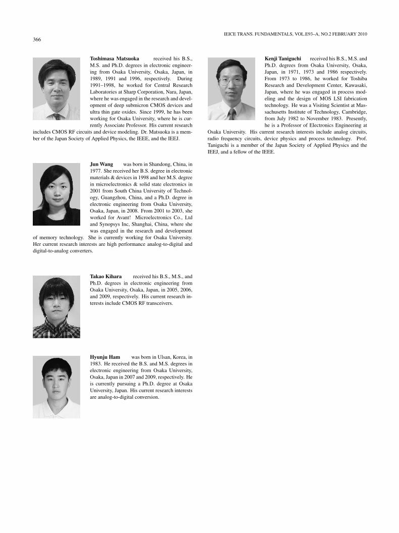
Toshimasa Matsuoka received his B.S.,M.S. and Ph.D. degrees in electronic engineer-ing from Osaka University, Osaka, Japan, in1989, 1991 and 1996, respectively. During1991–1998, he worked for Central ResearchLaboratories at Sharp Corporation, Nara, Japan,where he was engaged in the research and devel-opment of deep submicron CMOS devices andultra thin gate oxides. Since 1999, he has beenworking for Osaka University, where he is cur-rently Associate Professor. His current research
includes CMOS RF circuits and device modeling. Dr. Matsuoka is a mem-ber of the Japan Society of Applied Physics, the IEEE, and the IEEJ.
Jun Wang was born in Shandong, China, in1977. She received her B.S. degree in electronicmaterials & devices in 1998 and her M.S. degreein microelectronics & solid state electronics in2001 from South China University of Technol-ogy, Guangzhou, China, and a Ph.D. degree inelectronic engineering from Osaka University,Osaka, Japan, in 2008. From 2001 to 2003, sheworked for Avant! Microelectronics Co., Ltdand Synopsys Inc, Shanghai, China, where shewas engaged in the research and development
of memory technology. She is currently working for Osaka University.Her current research interests are high performance analog-to-digital anddigital-to-analog converters.
Takao Kihara received his B.S., M.S., andPh.D. degrees in electronic engineering fromOsaka University, Osaka, Japan, in 2005, 2006,and 2009, respectively. His current research in-terests include CMOS RF transceivers.
Hyunju Ham was born in Ulsan, Korea, in1983. He received the B.S. and M.S. degrees inelectronic engineering from Osaka University,Osaka, Japan in 2007 and 2009, respectively. Heis currently pursuing a Ph.D. degree at OsakaUniversity, Japan. His current research interestsare analog-to-digital conversion.
Kenji Taniguchi received his B.S., M.S. andPh.D. degrees from Osaka University, Osaka,Japan, in 1971, 1973 and 1986 respectively.From 1973 to 1986, he worked for ToshibaResearch and Development Center, Kawasaki,Japan, where he was engaged in process mod-eling and the design of MOS LSI fabricationtechnology. He was a Visiting Scientist at Mas-sachusetts Institute of Technology, Cambridge,from July 1982 to November 1983. Presently,he is a Professor of Electronics Engineering at
Osaka University. His current research interests include analog circuits,radio frequency circuits, device physics and process technology. Prof.Taniguchi is a member of the Japan Society of Applied Physics and theIEEJ, and a fellow of the IEEE.