Embed Size (px)
Citation preview
D E P A R T M E N T O F E L E C T R O N I C S A N D C O M M U N I C A T I O N E N G I N E E R I N G
Page 1
VLSI LAB MANUAL (10ECL77) 2017 - 18
INTRODUCTION TO VLSI LAB
VLSI lab allows the theoretical concepts studied as part of subjects CMOS VLSI
Design, Microelectronics Circuits and HDL, to experience in practical with the help of
Cadence tool framework. The lab introduces the complete custom IC design flow, ASIC
design flow and AMS (Analog and Mixed Signal) flow for Analog circuits, Digital circuits
and Analog and mixed signal circuits design respectively.
The analog design involves schematic (standard cell), test schematic capture and
symbolic representation of circuit topologies using Virtuoso schematic editor/ Composer.
Simulation of the test circuit to perform various analyses such as transient, DC and AC is
facilitated by Multimode Simulator/Spectre. Once the simulation results are obtained as per
the specifications the physical design is carried out using Virtuoso Layout suite followed by
the physical verification using Assura DRC (Design Rule Check), LVS (Layout Versus
Schematic) and Parasitic RC extraction. The floor planning, Power planning, placement and
routing can be performed later using Encounter.
The digital design involves the realization of various digital circuit components
using Register Transfer Logic (RTL) code, Compilation of the same using Native Compiler,
elaboration using elaborator and simulation using Incisive. The synthesis of the verified
RTL code to obtain the gate level netlist is performed thereon.
The AMS circuit design is performed by importing the digital modules as
configuration files into the analog environment, followed by the steps of the analog design
and simulating the same using AMS simulator instead of Spectre.
Introduction to Cadence Design Systems
Cadence is an Electronic Design Automation (EDA) environment which allows
different applications and tools to integrate into a single framework thus allowing
supporting all the stages of IC design and verification from a single environment. These
tools are completely general, supporting different fabrication technologies. When a
particular technology is selected, a set of configuration and technology-related files are
employed for customizing the cadence environment. This set of files is commonly referred
to as a design kit. The Cadence Development System consists of a bundle of software
packages such as schematic editors, simulators, and layout editors. This software manages
the development process for analog, digital, and mixed-mode circuits. In this lab, we will
D E P A R T M E N T O F E L E C T R O N I C S A N D C O M M U N I C A T I O N E N G I N E E R I N G
Page 2
VLSI LAB MANUAL (10ECL77) 2017 - 18
strictly use the tools associated with analog circuit design and digital design. All the
Cadence design tools are managed by a software package called the Design Framework II.
This program supervises a common database which holds all circuit information including
schematics, layouts, and simulation data.
LINUX Operating System
Using the LINUX operating system is similar to using other operating systems such
as DOS. LINUX commands are issued to the system by typing them in a “shell”. LINUX
commands are case sensitive so be careful when issuing a command, usually they are given
in lower-case.
The following list summarizes all the basic commands required to manage the data
files you will be creating in this lab course. All LINUX commands are entered from the
shell window (Terminal window).
Caution: Do not use LINUX commands for modifying, deleting, or moving any Cadence
data files.
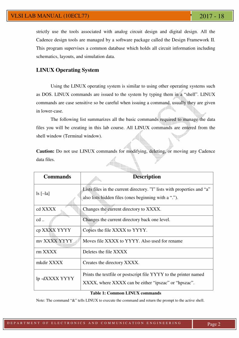
Commands Description
ls [–la] Lists files in the current directory. ”l” lists with properties and “a”
also lists hidden files (ones beginning with a “.”).
cd XXXX Changes the current directory to XXXX.
cd .. Changes the current directory back one level.
cp XXXX YYYY Copies the file XXXX to YYYY.
mv XXXX YYYY Moves file XXXX to YYYY. Also used for rename
rm XXXX Deletes the file XXXX
mkdir XXXX Creates the directory XXXX.
lp -dXXXX YYYY Prints the textfile or postscript file YYYY to the printer named
XXXX, where XXXX can be either “ipszac” or “hpszac”.
Table 1: Common LINUX commands
Note: The command “&” tells LINUX to execute the command and return the prompt to the active shell.
D E P A R T M E N T O F E L E C T R O N I C S A N D C O M M U N I C A T I O N E N G I N E E R I N G
Page 3
VLSI LAB MANUAL (10ECL77) 2017 - 18
ANALOG DESIGN
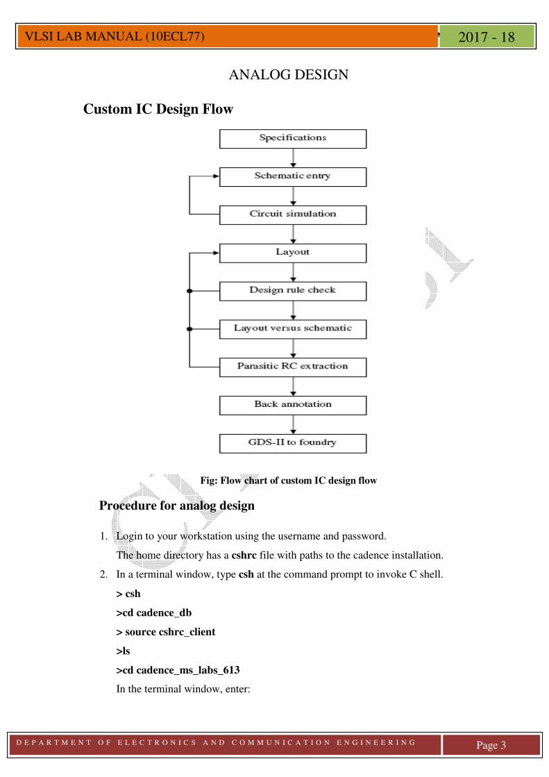
Custom IC Design Flow
Fig: Flow chart of custom IC design flow
Procedure for analog design
1. Login to your workstation using the username and password.
The home directory has a cshrc file with paths to the cadence installation.
2. In a terminal window, type csh at the command prompt to invoke C shell.
> csh
>cd cadence_db
> source cshrc_client
>ls
>cd cadence_ms_labs_613
In the terminal window, enter:

D E P A R T M E N T O F E L E C T R O N I C S A N D C O M M U N I C A T I O N E N G I N E E R I N G
Page 4
VLSI LAB MANUAL (10ECL77) 2017 - 18
>virtuoso &
The virtuoso or Command Interpreter Window (CIW) appears at the bottom of
the screen.
3. If the “What’s New…” window appears, close it with the File-Close command.
4. Keep opened CIW window for the labs.
Creating a new Library:
1. In the CIW window click on Tools-Library manager. The library manager window
will be opened.
2. Click File-New-Library. Specify the name for the new library. Click ok.
3. In the next “Technology File for New Library” form, select option Attach an
existing techfile and click ok.
4. In the “Attach Design Library to technology file” form, select gpdk180 from the
cyclic field and click ok
5. After creating a new library you can verify it from the Library manager.
Creating a Schematic Cellview:
1. In the CIW or Library manager, execute File-New-Cellview.
2. Setup the new file form.
3. Click ok. A blank schematic window for the design appears.
Adding Components to Schematics:
1. In the design window click the Instance fix menu icon to display add instance form.
2. Click on the browse button. This opens up a library browser from which you can
select the components and the symbol view.
3. After you complete the add instance form, move your cursor to the schematic
window and click left to place a component. If you place a component with wrong
parameter values, use the Edit-Properties-Objects command to change the
parameter. Use Edit-Move command if you place components in the wrong
location. You can rotate components using Edit-Rotate command.
4. After entering components, click cancel in the Add instance form or press Esc.
Adding Pins to Schematic:
1. Click the Pin fixed menu icon in the schematic window.
2. Make sure that the direction field is set to input/output/inout when placing the pins
respectively.
3. Select cancel from the Add-Pin form after placing the pins.
D E P A R T M E N T O F E L E C T R O N I C S A N D C O M M U N I C A T I O N E N G I N E E R I N G
Page 5
VLSI LAB MANUAL (10ECL77) 2017 - 18
Adding Wires to a Schematic:
1. Click the wire (narrow) icon in the schematic window.
2. In the schematic window, click on a pin of one of your components as the first point
for your wiring. A diamond shape appears over the starting point of this wire.
3. Follow the prompts at the bottom of the design window and click left on the
destination point for your wire. A wire is routed between the source and destination
points.
4. Complete the wiring as shown in figure and when done wiring press ESC key in the
schematic window to cancel wiring.
5. Click the Check and Save icon in the Schematic editor window.
6. Observe the CIW output area for any errors.
Symbol Creation:
1. In the schematic window, execute
Create -Cellview -From Cellview.
The Cellview form appears. With the Edit options function active, you can control
the appearance of the symbol to generate.
2. Verify that the From View Name field is set to schematic, and the To View Name
field is set to symbol, with the Tool/Data Type set as Schematic symbol. Click ok.
3. Modify the pin specification.
4. Click ok.
Editing a Symbol:
1. Move the cursor over the automatically generated symbol, until the green rectangle
is highlighted, click left to select it.
2. Click Delete icon in the symbol window, similarly select the red rectangle and delete
that.
3. Execute Create-Shape-Polygon.
4. After creating the shape press ESC key.
5. You can move the pin names according to the location.
6. Execute Create-Selection Box. In the Add Selection Box form, click Automatic. A
new red selection box is automatically added.
7. After creating symbol, click on the save icon in the symbol editor window to save
the symbol. In the symbol editor, execute File-Close to close the symbol view
window.
Simulation with Spectre:
1. In the schematic window, execute Launch-ADE L
2. In the simulation window execute Setup- Simulator/Directory/Host.
3. In the choosing simulator form, set the simulator field to Spectre and click ok.
4. In the simulation window execute setup-Model Libraries.
D E P A R T M E N T O F E L E C T R O N I C S A N D C O M M U N I C A T I O N E N G I N E E R I N G
Page 6
VLSI LAB MANUAL (10ECL77) 2017 - 18
5. Click the Browse button to add gpdk.scs if not added by default as shown in the
Model Library setup form, remember to select the section type as start in front of
gpdk.scs file. Click ok.
6. Click the Choose- Analysis icon .
7. To setup for transient analysis select tran icon, click at the moderate or enabled
button at the bottom, click Apply.
8. To setup for DC analysis select dc, turn on Save Dc Operating Point. Turn on the
Component Parameter. Click the select Component, which takes you to the
schematic window. Select input signal, Vpulse or DC analysis. Select start and stop
voltages. Click Apply and ok.
Selecting outputs for plotting:
1. Execute Outputs- To be plotted- Select on Schematic in the simulation window.
2. Follow the prompt at the bottom of the schematic window, click on the output net,
input net of the design. Press ESC with the cursor in the schematic after selecting it.
3. Execute Simulation-Netlist and Run to start the simulation.
Saving and Loading Simulator State:
1. In the simulation window, execute Session- Save State. Set the Save as field and
click ok.
2. In the simulation window execute Session- Load State, set the state name and click
ok.
Creating a Layout View:
1. From the schematic window menu execute Launch- Layout XL. A startup Option
form appears.
2. Select Create New option.
3. Check the cell name, View name. Click ok.
Adding Components to Layout:
1. Execute Connectivity-Generate-All from Source. Generate Layout form appears.
Click ok, which imports the schematic components into the layout window
automatically.
2. Rearrange the components within PR boundary.
3. To rotate a component, select the component and execute Edit-Properties. Now
select the degree of rotation.
4. To move a component, select the component and execute Edit-Move command.
Making Interconnection:
D E P A R T M E N T O F E L E C T R O N I C S A N D C O M M U N I C A T I O N E N G I N E E R I N G
Page 7
VLSI LAB MANUAL (10ECL77) 2017 - 18
1. Execute Connectivity-Nets-Show/Hide Selected incomplete nets.
2. Move the mouse pointer over the device and click LMB to get the connectivity
information, which shows the guidelines for the interconnections of the components.
3. From the layout window execute Create-Shape-Path or Create-Shape-Rectangle
and select the appropriate layers from the LSW window and Vias for making
interconnections.
Creating Contacts/Vias:
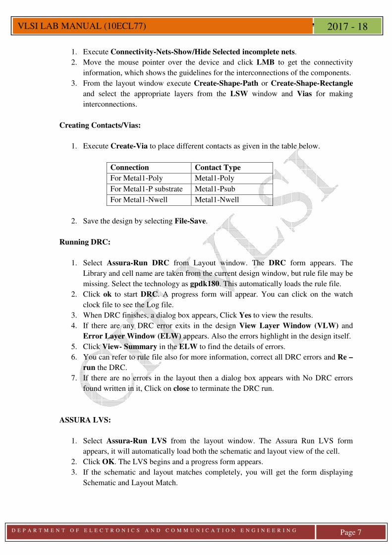
1. Execute Create-Via to place different contacts as given in the table below.
Connection Contact Type
For Metal1-Poly Metal1-Poly
For Metal1-P substrate Metal1-Psub
For Metal1-Nwell Metal1-Nwell
2. Save the design by selecting File-Save.
Running DRC:
1. Select Assura-Run DRC from Layout window. The DRC form appears. The
Library and cell name are taken from the current design window, but rule file may be
missing. Select the technology as gpdk180. This automatically loads the rule file.
2. Click ok to start DRC. A progress form will appear. You can click on the watch
clock file to see the Log file.
3. When DRC finishes, a dialog box appears, Click Yes to view the results.
4. If there are any DRC error exits in the design View Layer Window (VLW) and
Error Layer Window (ELW) appears. Also the errors highlight in the design itself.
5. Click View- Summary in the ELW to find the details of errors.
6. You can refer to rule file also for more information, correct all DRC errors and Re –
run the DRC.
7. If there are no errors in the layout then a dialog box appears with No DRC errors
found written in it, Click on close to terminate the DRC run.
ASSURA LVS:
1. Select Assura-Run LVS from the layout window. The Assura Run LVS form
appears, it will automatically load both the schematic and layout view of the cell.
2. Click OK. The LVS begins and a progress form appears.
3. If the schematic and layout matches completely, you will get the form displaying
Schematic and Layout Match.
D E P A R T M E N T O F E L E C T R O N I C S A N D C O M M U N I C A T I O N E N G I N E E R I N G
Page 8
VLSI LAB MANUAL (10ECL77) 2017 - 18
4. If the schematic and Layout do not matches, a form informs that the LS completed
successfully and results form will appear, click YES in the form.
5. In the LVS debug form, find the details of mismatches and correct all those
mismatches and Re-Run the LVS.
ASSURA RCX:
1. From the layout window execute Assura-Run QRC.
2. Change the Assura Parasitic Extraction form, select Output Type under Setup tab
of the form.
3. In the Extraction tab of the form, choose Extraction type, Cap coupled mode and
specify the reference node for extraction.
4. In the filtering tab of the form, Enter Power Nets as Vdd!, Vss! and Enter Ground
Nets as gnd!
5. Click ok. The RCX progress form appears, in the progress form click Watch log file
to see the output log file.
6. When RCX completes, a dialog box appears, shows Assura RCX Run completed
successfully.
7. Open the av_extracted view from the Library manager and view the parasitic.
Configuration View:
1. In the CIW or Library manager, execute File-New-Cell view.
2. Click ok in Create New File form. The Hierarchy editor form opens and a New
Configuration form opens in front of it.
3. Click Use template at the bottom of the New Configuration form and select
Spectre in the cyclic field and click ok.
4. Change the Top Cell view to schematic and remove the default entry from the
Library List field.
5. Click ok. The Hierarchy editor displays the Hierarchy for the design using table
format.
6. Click the Tree View tab. The Design hierarchy changes to Tree format. Save the
current configuration.
7. Close the Hierarchy window, execute File-Close window.
To run the circuit without parasites:
1. From the Library manager open cell config view.
2. In the form, turn on the both cyclic buttons to Yes and click ok.
3. Execute Launch-ADE L from the schematic window.
4. Follow the same procedure for running the simulation. Execute Session-Load state.
5. Click Netlist and Run icon to start the simulation.
D E P A R T M E N T O F E L E C T R O N I C S A N D C O M M U N I C A T I O N E N G I N E E R I N G
Page 9
VLSI LAB MANUAL (10ECL77) 2017 - 18
6. In the CIW, note the netlisting statistics in the circuit inventory section. This list
includes all nets, design devices, source and loads. There are no parasitic
components.
Measuring the Propagation Delay:
1. In the waveform window execute Tools-Calculator.
2. From the functions select delay, this will open the delay data panel.
3. Place the cursor in the text box for signal1, select the wave button and select the
input waveform from the waveform window.
4. Repeat the same for signal2, select the output form.
5. Set the Threshold value1 and Threshold value2.
6. Execute ok and observe the expression created in the calculator.
7. Click on Evaluate the Buffer icon to perform the calculation. Close calculator
window.
D E P A R T M E N T O F E L E C T R O N I C S A N D C O M M U N I C A T I O N E N G I N E E R I N G
Page 10
VLSI LAB MANUAL (10ECL77) 2017 - 18
DIGITAL DESIGN
1. Login to your workstation using the username and password.
The home directory has a cshrc file with paths to the cadence installation.
2. In a terminal window, type csh at the command prompt to invoke C shell.
> csh
> cd cadence_db
> source cshrc_client
> cd Cadence_digital_labs
> cd Workarea
3. Create the directory by USN using a command mkdir USN
4. Enter the directory by using a command cd USN.
5. Create a new directory for each program using command mkdir programname.
6. Enter to the program directory using command cd programname.
7. Create a file to write a code using command vi filename.v Ex: vi inverter.v
8. Create a file to write a testbench using command vi filename_t.v Ex: vi inverter_t.v
9. Use :wq command to save and exit the file.
10 Create the local library directory. Ex mkdir design.lib
11 Create the cds.lib(vi cds.lib) file and make the following entry.
Ex: Define design_lib ./design.lib
12 Create the hdl.var file and make the following entry.
Ex: Define WORK design_lib
Define NCELABOPTS -messages
13. Compile the code using ncvlog filename.v –MESS. Ex: ncvlog inverter.v –MESS
14. Compile the test bench using ncvlog filename_t.v –MESS.
Ex: ncvlog inverter_t.v –MESS
15. Elaborate the testbench once again to place the testcode and snapshot in local library
using command ncelab topmodulename(of test bench) –access +rwc -MESS.
16. Simulate the testbench with gui option: ncsim topmodulename(of test bench) –gui.
17. Once the simulation is done see the waveform window and console window with the
outputs.
D E P A R T M E N T O F E L E C T R O N I C S A N D C O M M U N I C A T I O N E N G I N E E R I N G
Page 11
VLSI LAB MANUAL (10ECL77) 2017 - 18
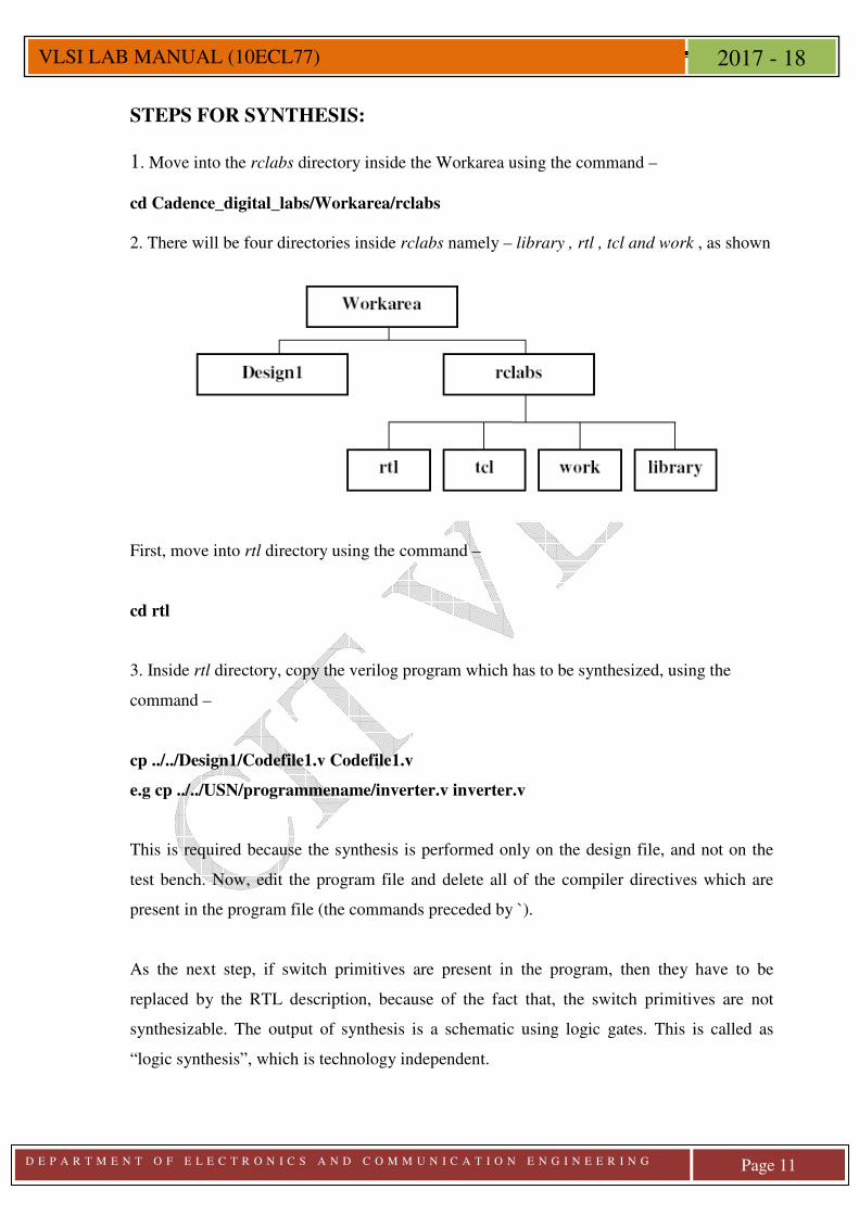
STEPS FOR SYNTHESIS: 1. Move into the rclabs directory inside the Workarea using the command – cd Cadence_digital_labs/Workarea/rclabs 2. There will be four directories inside rclabs namely – library , rtl , tcl and work , as shown
First, move into rtl directory using the command –
cd rtl
3. Inside rtl directory, copy the verilog program which has to be synthesized, using the
command –
cp ../../Design1/Codefile1.v Codefile1.v
e.g cp ../../USN/programmename/inverter.v inverter.v
This is required because the synthesis is performed only on the design file, and not on the
test bench. Now, edit the program file and delete all of the compiler directives which are
present in the program file (the commands preceded by `).
As the next step, if switch primitives are present in the program, then they have to be
replaced by the RTL description, because of the fact that, the switch primitives are not
synthesizable. The output of synthesis is a schematic using logic gates. This is called as
“logic synthesis”, which is technology independent.
D E P A R T M E N T O F E L E C T R O N I C S A N D C O M M U N I C A T I O N E N G I N E E R I N G
Page 12
VLSI LAB MANUAL (10ECL77) 2017 - 18
4. Then come out of that directory using the command –
cd ../
5. Now enter into the tcl directory using the command – cd tcl 6. Inside tcl directory there is a file named setup.g . Open this file using the command – gedit setup.g & 7. In this file, you have to update two variables –
(a) FILE_LIST {filename} e.g: FILE_LIST {Codefile1.v}
(b) DESIGN modulename
Save the setup.g file and come out of tcl directory.
8. Next, enter into the directory work . Create a file named Contraints_file.g . The timing
constraints are defined in this file. Example of one such file is as shown –
create_clock -name clk -period 10 -waveform {0 5} [get_ports "clk"]
set_clock_transition -rise 0.1 [get_clocks "clk"]
set_clock_transition -fall 0.1 [get_clocks "clk"]
set_clock_uncertainty 1.0 [get_ports "clk"]
set_input_delay -max 1.0 [get_ports "A"] -clock [get_clocks "clk"]
set_input_delay -max 1.0 [get_ports "B"] -clock [get_clocks "clk"]
set_output_delay -max 1.0 [get_ports "sum"] -clock [get_clocks "clk"]
There are three different parts in the constraint file:
a. Clock definition and clock constraints –
create_clock -name clk -period 10 -waveform {0 5} [get_ports "clock"] �Clock definition
set_clock_transition -rise 0.1 [get_clocks " clk "] �Clock rise time
set_clock_transition -fall 0.1 [get_clocks " clk "] � Clock fall time
D E P A R T M E N T O F E L E C T R O N I C S A N D C O M M U N I C A T I O N E N G I N E E R I N G
Page 13
VLSI LAB MANUAL (10ECL77) 2017 - 18
set_clock_uncertainty 1.0 [get_ports " clk "] � Uncertainties of Clock
b. Input port timing constraints –
set_input_delay -max 1.0 [get_ports " A"] -clock [get_clocks " clk "]� Input port delay
set_input_delay -max 1.0 [get_ports " B"] -clock [get_clocks " clk "] � Input port delay
c. Output port timing constraints –
set_output_delay -max 1.0 [get_ports " sum "] -clock [get_clocks " clk "]�Output port
delay
The port names that are used in the constraint file (bolded) must match with the names that
are used in the Verilog program of the main design module. The constraints are defined for
all the ports in the design.
9. Now, invoke the Encounter tool using the command –
rc –gui
The tool will be invoked and you will get the rc prompt in the terminal, along with a
synthesis window. Next, the following commands are to be typed in the rc prompt –
1. include ../tcl/setup.g
2. set_attribute library $LIBRARY
3. set SYN_EFF medium
4. set MAP_EFF medium
5. read_hdl $FILE_LIST
6. elaborate $DESIGN
7. read_sdc ./Constraints_file.g
8. synthesize -to_generic -eff $SYN_EFF
9. report timing
10. report area
11. report power
D E P A R T M E N T O F E L E C T R O N I C S A N D C O M M U N I C A T I O N E N G I N E E R I N G
Page 14
VLSI LAB MANUAL (10ECL77) 2017 - 18
11. The tool will execute each command as and when it is entered. To come out of the
synthesis environment, exit or quit command in the rc prompt is used.
12. The commands of step-10 can be saved in a .tcl file in the work directory, and that
script file can be invoked in the rc prompt, by using the include command. Optionally, the
synthesis can be performed by going to the GUI window and clicking on File, and then
clicking on Source Script, and then selecting the respective script file.
NOTES 1. Linux commands:
ls list files cp copy files
mv rename files rm remove files
cd change directory pwd print working directory
mkdir make directory rmdir remove directory
When ls command is given, the directories are displayed in blue color, the files in black color, the link files in green color, and the tar files in red color respectively. 2. Command options:
~ � for root directory
. � for present directory
.. � for parent directory
-mess � for displaying messages
+rwc � for obtaining read, write, compilation access
& � for making the process a background one
3. Abbreviations:
GDS Generic Data Stream
IUS Incisive Unified Simulator
NC Native compiler
RC RTL compiler
RTL Register Transfer Level
TCL Tool Command Language
4. Cadence tools used:
IUS and Simvision - to compile, elaborate and simulate
rc and Encounter - for RTL Compilation & Synthesis
D E P A R T M E N T O F E L E C T R O N I C S A N D C O M M U N I C A T I O N E N G I N E E R I N G
Page 15
VLSI LAB MANUAL (10ECL77) 2017 - 18
LAB 1: INVERTER
Objective: To design an Inverter with given specifications and verifying the following
1. Schematic: i) DC Analysis ii) Transient Analysis
2. Layout: i) DRC ii) LVS iii) RCX
Design:
Device Cutoff Non saturation Saturation
P device
Vgsp>Vtp Vin > Vtp+Vdd
Vgsp<Vtp Vin < Vtp+Vdd Vdsp>Vgsp-Vtp Vout> Vin-Vtp
Vgsp<Vtp Vin<Vtp+Vdd Vdsp<Vgsp-Vtp Vout<Vin-Vtp
n device
Vgsn<Vtn Vin<Vtn
Vgsn>Vtn Vin> Vtn Vdsn<Vgs-Vtn Vout<Vin-Vtn
Vgsn>Vtn Vin>Vtn Vdsn>Vgs-Vtn Vout>Vin-Vtn
Region A: 0<= Vin<= Vtn, Vout=Vdd;
Region B: Vtn<= Vin<Vdd/2, Idsn=βn2
)( 2VtnVin −
Idsp= - βp[(Vin-Vdd-Vtp)(Vout-Vdd)- 2
)( 2VddVout −
]
Vout = (Vin-Vtp)+p
nVddVtp
VddVinVtpVin
β
β−−−−− )
2(2)( 2 2)( VtnVin −
Region C: Vin = Vdd/2, Idsp = - 2)(2
VtpVddVinp
−−β
Idsn= 2)(2
VtnVinn
−β
, With βn=βp and Vtn =-Vtp
Vin = Vdd/2
Region D: Vdd/2 < Vin<=Vdd+Vtp, Idsp = - 2)(2
VtpVddVinp
−−β
Idsn= ]2
)[(2
VoutVoutVtnVinn −−β
Vout = 22 )()()( VtpVddVinn
pVtnVinVtnVin −−−−−−
β
β
Region E: Vin>= Vdd-Vtp, Vout = 0
D E P A R T M E N T O F E L E C T R O N I C S A N D C O M M U N I C A T I O N E N G I N E E R I N G
Page 16
VLSI LAB MANUAL (10ECL77) 2017 - 18
Region Condition P device n device A 0≤Vin< Vtn Nonsaturation Cutoff
B Vtn≤ Vin<Vdd/2 Nonsaturation Saturation
C Vin=Vdd/2 Saturation Saturation
D Vdd/2<Vin≤Vdd - Vtp| Saturation Nonsaturation
E Vin>Vdd-|Vtp| Cutoff Nonsaturation
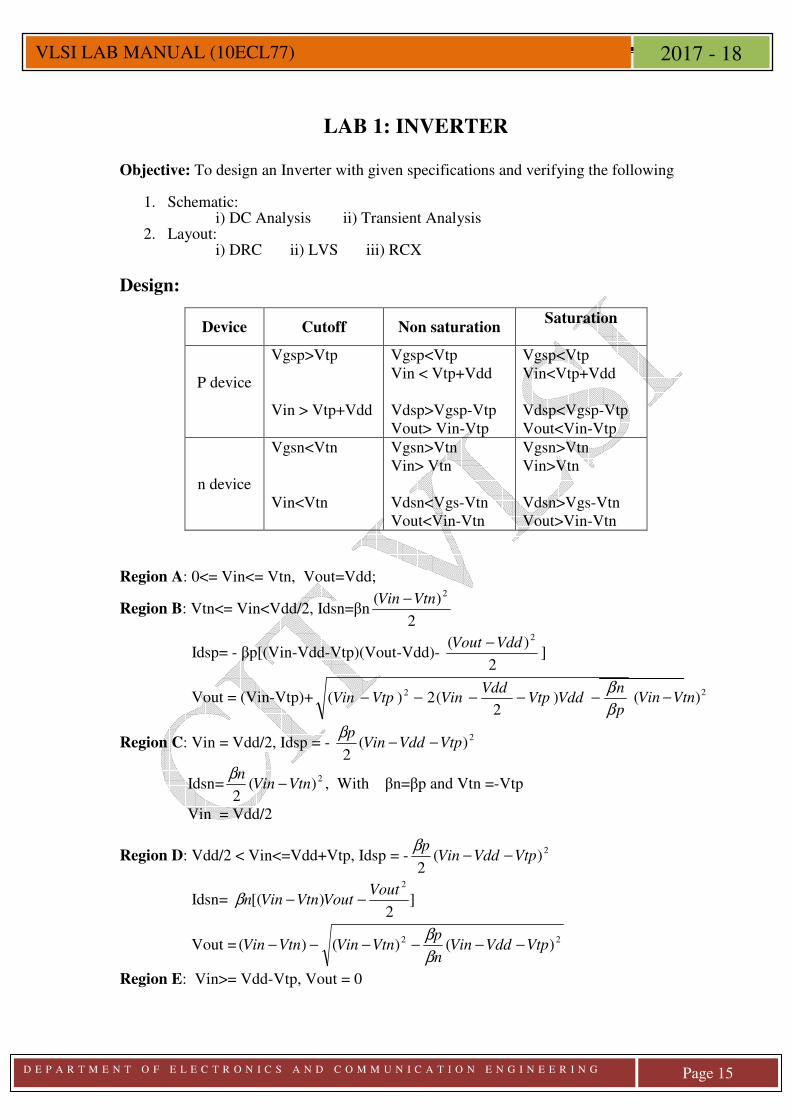
Inverter Schematic: Specifications:
Library name Cell name Properties gpdk180 pmos W=2µ, L=180n
gpdk180 nmos W=2µ, L=180n
Pin Names Direction Vin Input
Vout Output
vdd vss Input
Figure 1: Inverter Schematic
D E P A R T M E N T O F E L E C T R O N I C S A N D C O M M U N I C A T I O N E N G I N E E R I N G
Page 17
VLSI LAB MANUAL (10ECL77) 2017 - 18
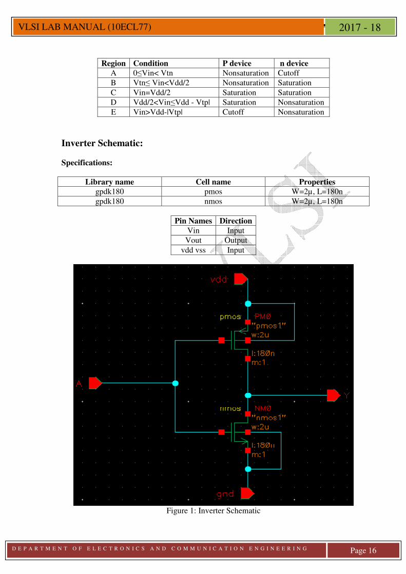
Inverter_test Schematic: Specifications:
Library name Cell name Properties
analoglib Vpulse V1=0,V2=1.8,td=0,tr=tf=1ns, pulse width=10n, Period=20ns
analoglib Vdc Vdc=1.8
analoglib Gnd -
Analysis Values
Transient Stop time = 200ns
Dc Start time =0, stop time =2.
Figure 2: Inverter_test Schematic
Result
Figure 3(a): Transient response Figure 3(a): DC response
D E P A R T M E N T O F E L E C T R O N I C S A N D C O M M U N I C A T I O N E N G I N E E R I N G
Page 18
VLSI LAB MANUAL (10ECL77) 2017 - 18
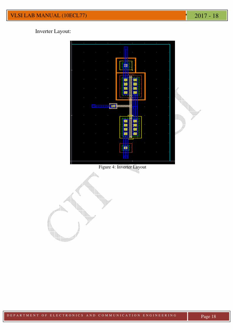
Inverter Layout:
Figure 4: Inverter Layout
D E P A R T M E N T O F E L E C T R O N I C S A N D C O M M U N I C A T I O N E N G I N E E R I N G
Page 19
VLSI LAB MANUAL (10ECL77) 2017 - 18
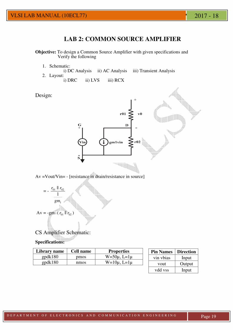
LAB 2: COMMON SOURCE AMPLIFIER
Objective: To design a Common Source Amplifier with given specifications and Verify the following
1. Schematic: i) DC Analysis ii) AC Analysis iii) Transient Analysis
2. Layout: i) DRC ii) LVS iii) RCX
Design:
Av =Vout/Vin= - [resistance in drain/resistance in source]
= -
1
0201
1
||
gm
rr
Av = -gm 1 ( 0201 || rr )
CS Amplifier Schematic:
Specifications:
Library name Cell name Properties gpdk180 pmos W=50µ, L=1µ
gpdk180 nmos W=10µ, L=1µ
Pin Names Direction
vin vbias Input
vout Output
vdd vss Input
D E P A R T M E N T O F E L E C T R O N I C S A N D C O M M U N I C A T I O N E N G I N E E R I N G
Page 20
VLSI LAB MANUAL (10ECL77) 2017 - 18
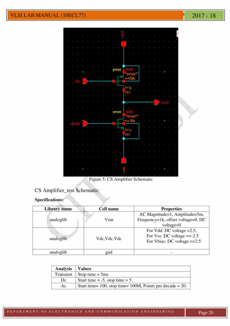
Figure 5: CS Amplifier Schematic
CS Amplifier_test Schematic:
Specifications:
Library name Cell name Properties
analoglib Vsin AC Magnitude=1, Amplitude=5m,
Frequency=1k, offset voltage=0, DC voltage=0
analoglib Vdc,Vdc,Vdc
For Vdd: DC voltage =2.5, For Vss: DC voltage ==-2.5 For Vbias: DC voltage ==2.5
analoglib gnd -
Analysis Values
Transient Stop time = 5ms
Dc Start time = -5, stop time = 5.
Ac Start time= 100, stop time= 100M, Points per decade = 20.
D E P A R T M E N T O F E L E C T R O N I C S A N D C O M M U N I C A T I O N E N G I N E E R I N G
Page 21
VLSI LAB MANUAL (10ECL77) 2017 - 18
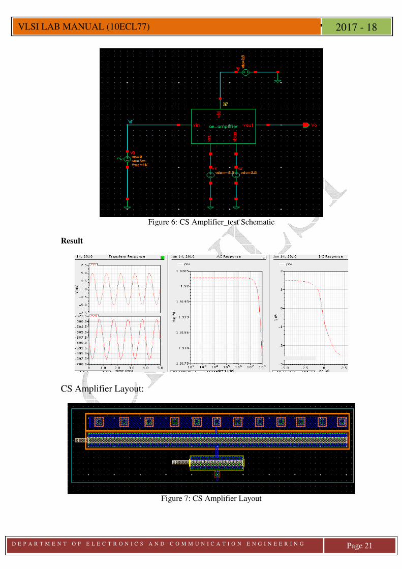
Figure 6: CS Amplifier_test Schematic
Result
CS Amplifier Layout:
Figure 7: CS Amplifier Layout
D E P A R T M E N T O F E L E C T R O N I C S A N D C O M M U N I C A T I O N E N G I N E E R I N G
Page 22
VLSI LAB MANUAL (10ECL77) 2017 - 18
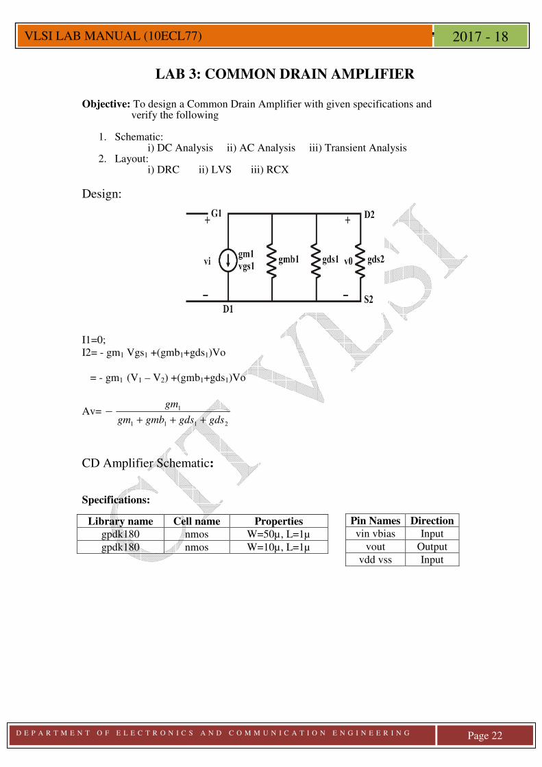
LAB 3: COMMON DRAIN AMPLIFIER
Objective: To design a Common Drain Amplifier with given specifications and verify the following
1. Schematic: i) DC Analysis ii) AC Analysis iii) Transient Analysis
2. Layout: i) DRC ii) LVS iii) RCX
Design:
I1=0; I2= - gm1 Vgs1 +(gmb1+gds1)Vo = - gm1 (V1 – V2) +(gmb1+gds1)Vo
Av= 2111
1
gdsgdsgmbgm
gm
+++
CD Amplifier Schematic:
Specifications:
Library name Cell name Properties gpdk180 nmos W=50µ, L=1µ
gpdk180 nmos W=10µ, L=1µ
Pin Names Direction vin vbias Input
vout Output
vdd vss Input
D E P A R T M E N T O F E L E C T R O N I C S A N D C O M M U N I C A T I O N E N G I N E E R I N G
Page 23
VLSI LAB MANUAL (10ECL77) 2017 - 18
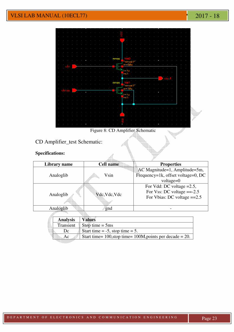
Figure 8: CD Amplifier Schematic
CD Amplifier_test Schematic: Specifications:
Library name Cell name Properties
Analoglib Vsin AC Magnitude=1, Amplitude=5m,
Frequency=1k, offset voltage=0, DC voltage=0
Analoglib Vdc,Vdc,Vdc
For Vdd: DC voltage =2.5, For Vss: DC voltage ==-2.5 For Vbias: DC voltage ==2.5
Analoglib gnd -
Analysis Values Transient Stop time = 5ms
Dc Start time = -5, stop time = 5.
Ac Start time= 100,stop time= 100M,points per decade = 20.
D E P A R T M E N T O F E L E C T R O N I C S A N D C O M M U N I C A T I O N E N G I N E E R I N G
Page 24
VLSI LAB MANUAL (10ECL77) 2017 - 18
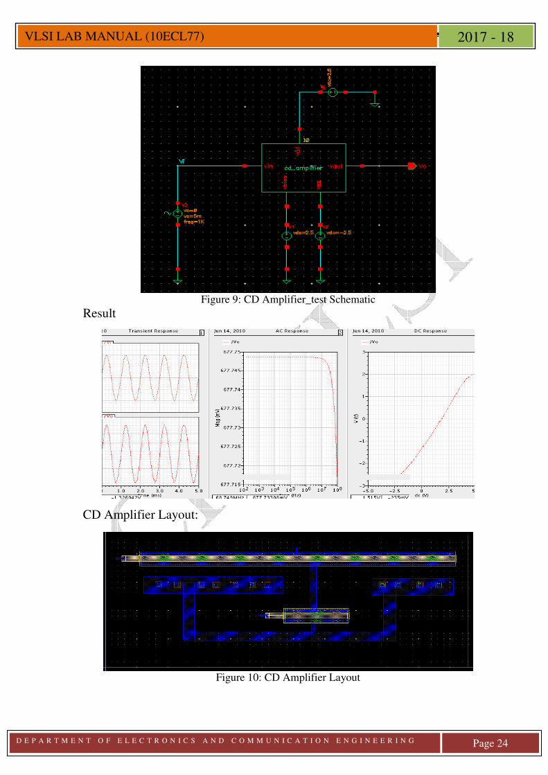
Figure 9: CD Amplifier_test Schematic
Result
CD Amplifier Layout:
Figure 10: CD Amplifier Layout
D E P A R T M E N T O F E L E C T R O N I C S A N D C O M M U N I C A T I O N E N G I N E E R I N G
Page 25
VLSI LAB MANUAL (10ECL77) 2017 - 18
LAB 4: DIFFERENTIAL AMPLIFIER
Objective: To design a single stage Differential Amplifier with given specifications and verifying the following
1. Schematic: i) DC Analysis ii) AC Analysis iii) Transient Analysis
2. Layout: i) DRC ii) LVS iii) RCX
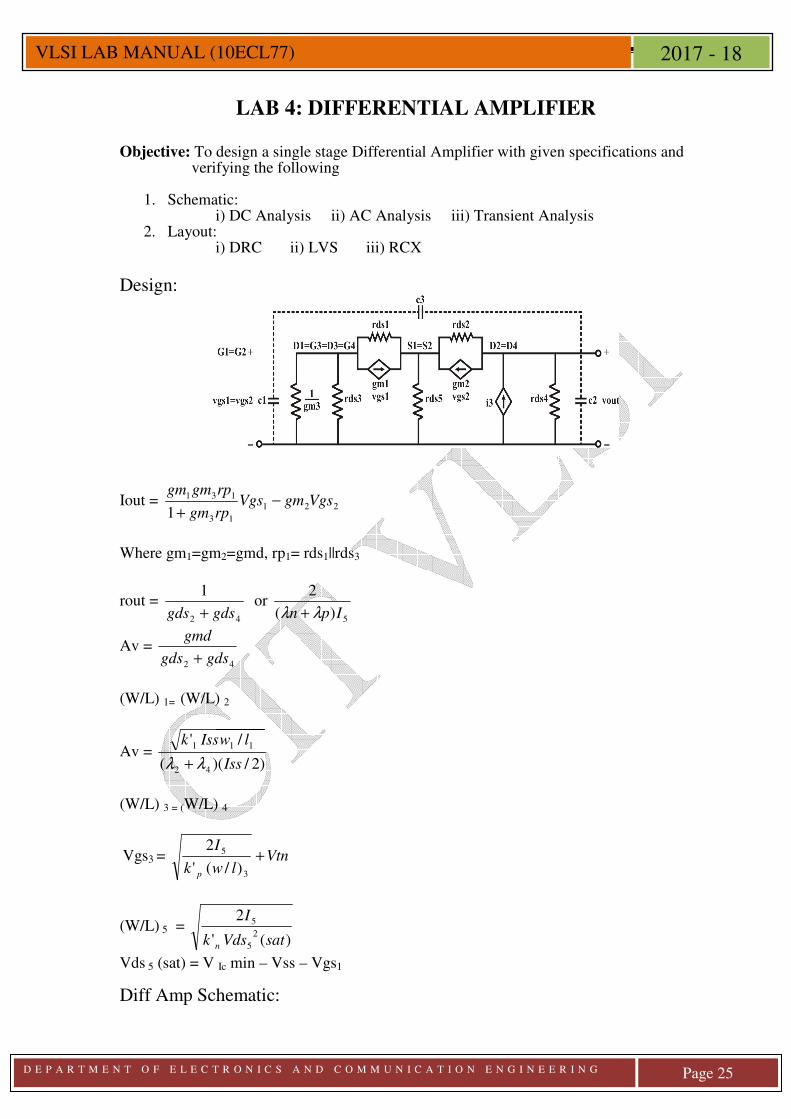
Design:
Iout = 221
13
131
1VgsgmVgs
rpgm
rpgmgm−
+
Where gm1=gm2=gmd, rp1= rds1||rds3
rout = 42
1
gdsgds + or
5)(
2
Ipn λλ +
Av = 42 gdsgds
gmd
+
(W/L) 1= (W/L) 2
Av = )2/)((
/'
42
111
Iss
lwIssk
λλ +
(W/L) 3 = (W/L) 4
Vgs3 = Vtnlwk
I
p
+3
5
)/('
2
(W/L) 5 = )('
22
5
5
satVdsk
I
n
Vds 5 (sat) = V Ic min – Vss – Vgs1
Diff Amp Schematic:
D E P A R T M E N T O F E L E C T R O N I C S A N D C O M M U N I C A T I O N E N G I N E E R I N G
Page 26
VLSI LAB MANUAL (10ECL77) 2017 - 18
Specification:
Library name
Cell name Properties
gpdk180 nmos Model name(NM0, NM1);
W=3µ, L=1µ
gpdk180 nmos Model name(NM2, NM3);
W=4.5µ, L=1µ
gpdk180 pmos Model name(PM0, PM1);
W=15µ, L=1µ
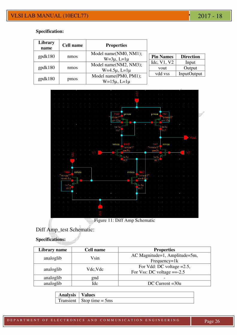
Figure 11: Diff Amp Schematic
Diff Amp_test Schematic:
Specifications:
Library name Cell name Properties
analoglib Vsin AC Magnitude=1, Amplitude=5m,
Frequency=1k
analoglib Vdc,Vdc For Vdd: DC voltage =2.5,
For Vss: DC voltage ==-2.5
analoglib gnd -
analoglib Idc DC Current =30u
Analysis Values Transient Stop time = 5ms
Pin Names Direction Idc, V1, V2 Input
vout Output
vdd vss InputOutput
D E P A R T M E N T O F E L E C T R O N I C S A N D C O M M U N I C A T I O N E N G I N E E R I N G
Page 27
VLSI LAB MANUAL (10ECL77) 2017 - 18
Dc Start time = -5, stop time = 5.
Ac Start time= 100,stop time= 100M,points per decade = 20.
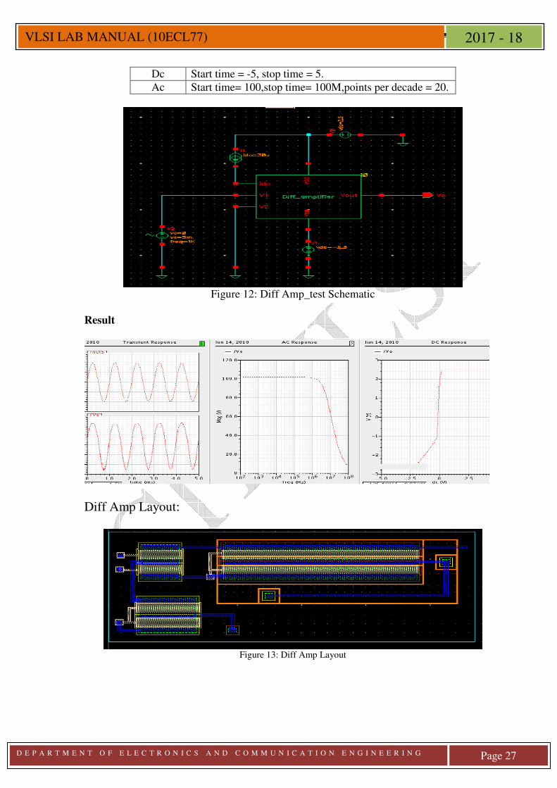
Figure 12: Diff Amp_test Schematic
Result
Diff Amp Layout:
Figure 13: Diff Amp Layout
D E P A R T M E N T O F E L E C T R O N I C S A N D C O M M U N I C A T I O N E N G I N E E R I N G
Page 28
VLSI LAB MANUAL (10ECL77) 2017 - 18
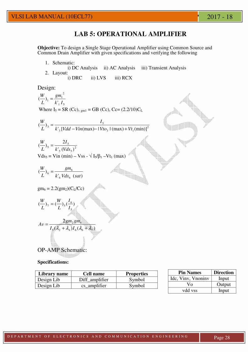
LAB 5: OPERATIONAL AMPLIFIER
Objective: To design a Single Stage Operational Amplifier using Common Source and Common Drain Amplifier with given specifications and verifying the following
1. Schematic: i) DC Analysis ii) AC Analysis iii) Transient Analysis
2. Layout: i) DRC ii) LVS iii) RCX
Design:
51
2
11
')(
Ik
gm
L
W=
Where I5 = SR (Cc), gm1 = GB (Cc), Cc= (2.2/10)CL
2
133
53
(min)](max)||(max)[')(
VtVtoVinVddk
I
L
W
+−−=
2
55
55
)('
2)(
Vdsk
I
L
W=
Vds5 = Vin (min) – Vss - √ I5/β1 –Vt1 (max)
)(')(
66
66
satVdsk
gm
L
W=
gm6 = 2.2(gm2)(CL/Cc)
)()()(5
657
I
I
L
W
L
W=
)()(
2
766425
62
λλλλ ++=
II
gmgmAv
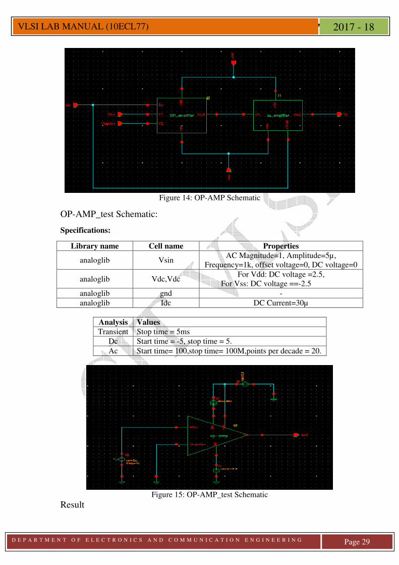
OP-AMP Schematic: Specifications: Library name Cell name Properties Design Lib Diff_amplifier Symbol
Design Lib cs_amplifier Symbol
Pin Names Direction Idc, Vinv, Vnoninv Input
Vo Output
vdd vss Input
D E P A R T M E N T O F E L E C T R O N I C S A N D C O M M U N I C A T I O N E N G I N E E R I N G
Page 29
VLSI LAB MANUAL (10ECL77) 2017 - 18
Figure 14: OP-AMP Schematic
OP-AMP_test Schematic:
Specifications:
Library name Cell name Properties
analoglib Vsin AC Magnitude=1, Amplitude=5µ,
Frequency=1k, offset voltage=0, DC voltage=0
analoglib Vdc,Vdc For Vdd: DC voltage =2.5,
For Vss: DC voltage ==-2.5
analoglib gnd -
analoglib Idc DC Current=30µ
Analysis Values Transient Stop time = 5ms
Dc Start time = -5, stop time = 5.
Ac Start time= 100,stop time= 100M,points per decade = 20.
Figure 15: OP-AMP_test Schematic
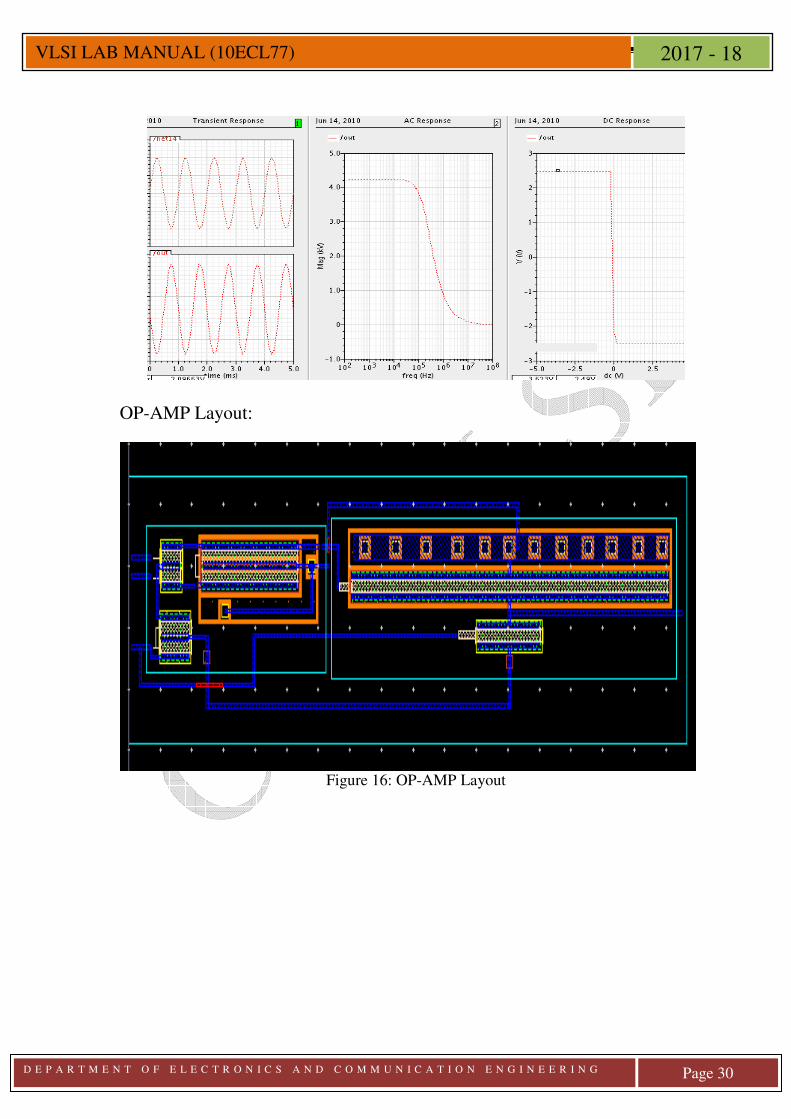
Result
D E P A R T M E N T O F E L E C T R O N I C S A N D C O M M U N I C A T I O N E N G I N E E R I N G
Page 30
VLSI LAB MANUAL (10ECL77) 2017 - 18
OP-AMP Layout:
Figure 16: OP-AMP Layout
D E P A R T M E N T O F E L E C T R O N I C S A N D C O M M U N I C A T I O N E N G I N E E R I N G
Page 31
VLSI LAB MANUAL (10ECL77) 2017 - 18
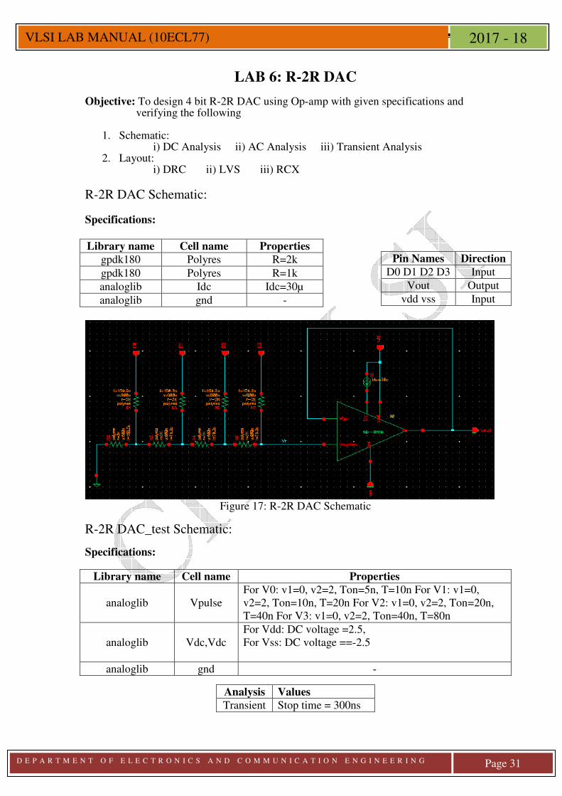
LAB 6: R-2R DAC
Objective: To design 4 bit R-2R DAC using Op-amp with given specifications and verifying the following
1. Schematic: i) DC Analysis ii) AC Analysis iii) Transient Analysis
2. Layout: i) DRC ii) LVS iii) RCX
R-2R DAC Schematic:
Specifications:
Library name Cell name Properties gpdk180 Polyres R=2k
gpdk180 Polyres R=1k
analoglib Idc Idc=30µ
analoglib gnd -
Figure 17: R-2R DAC Schematic
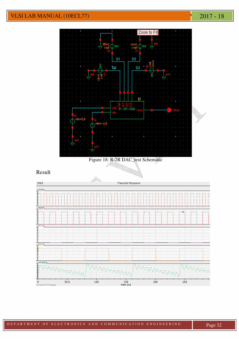
R-2R DAC_test Schematic:
Specifications:
Library name Cell name Properties
analoglib Vpulse For V0: v1=0, v2=2, Ton=5n, T=10n For V1: v1=0, v2=2, Ton=10n, T=20n For V2: v1=0, v2=2, Ton=20n, T=40n For V3: v1=0, v2=2, Ton=40n, T=80n
analoglib Vdc,Vdc For Vdd: DC voltage =2.5, For Vss: DC voltage ==-2.5
analoglib gnd -
Analysis Values Transient Stop time = 300ns
Pin Names Direction D0 D1 D2 D3 Input
Vout Output
vdd vss Input
D E P A R T M E N T O F E L E C T R O N I C S A N D C O M M U N I C A T I O N E N G I N E E R I N G
Page 32
VLSI LAB MANUAL (10ECL77) 2017 - 18
Figure 18: R-2R DAC_test Schematic
Result
D E P A R T M E N T O F E L E C T R O N I C S A N D C O M M U N I C A T I O N E N G I N E E R I N G
Page 33
VLSI LAB MANUAL (10ECL77) 2017 - 18
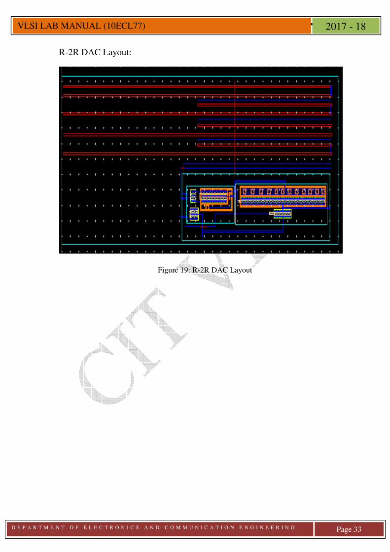
R-2R DAC Layout:
Figure 19: R-2R DAC Layout

D E P A R T M E N T O F E L E C T R O N I C S A N D C O M M U N I C A T I O N E N G I N E E R I N G
Page 34
VLSI LAB MANUAL (10ECL77) 2017 - 18
DIGITAL DESIGN
LAB 1: INVERTER Objective: To Compile and simulate the Verilog Code for an inverter circuit and observe the waveform.
Inverter: `resetall `timescale 1 ns / 1 ns `view vlog //Define our own Inverter, module inverter ( out , in ); // Declarations of I/O, Power and Ground Lines output out; input in; supply1 pwr; supply0 gnd; // Instantiate pmos and nmos switches pmos (out,pwr,in); nmos (out,gnd,in); endmodule `noview
Inverter_test: `resetall `timescale 1 ns / 1 ns `view vlog // Testbench for Inverter Module module inv_test; wire out ; reg in ; `uselib view = vlog // Instantiate inverter Module
D E P A R T M E N T O F E L E C T R O N I C S A N D C O M M U N I C A T I O N E N G I N E E R I N G
Page 35
VLSI LAB MANUAL (10ECL77) 2017 - 18
inverter i ( out, in ) ; `nouselib // Display task display ; begin $display ( "time=%0d" , $time , " ns" , " Input=" , in , " Output=", out ) ; end endtask // Apply Stimulus initial begin in = 1'b0 ; #10 ; display ; in = 1'b1 ; #10 ; display ; in = 1'bx ; #10 ; display ; in = 1'bz ; #10 ; display ; end endmodule `noview Note: The task “display” is used to display the output on the monitor, in the form of a truth table. For observing the waveforms, the Simvision tool can be invoked.
Constraints file for Synthesis: Constraints_Inverter.g set_input_delay -max 1.0 [get_ports "in"] set_output_delay -max 1.0 [get_ports "out"]
Truth Table
Input Output
A Y
0 1
1 0
X X
Z X
D E P A R T M E N T O F E L E C T R O N I C S A N D C O M M U N I C A T I O N E N G I N E E R I N G
Page 36
VLSI LAB MANUAL (10ECL77) 2017 - 18
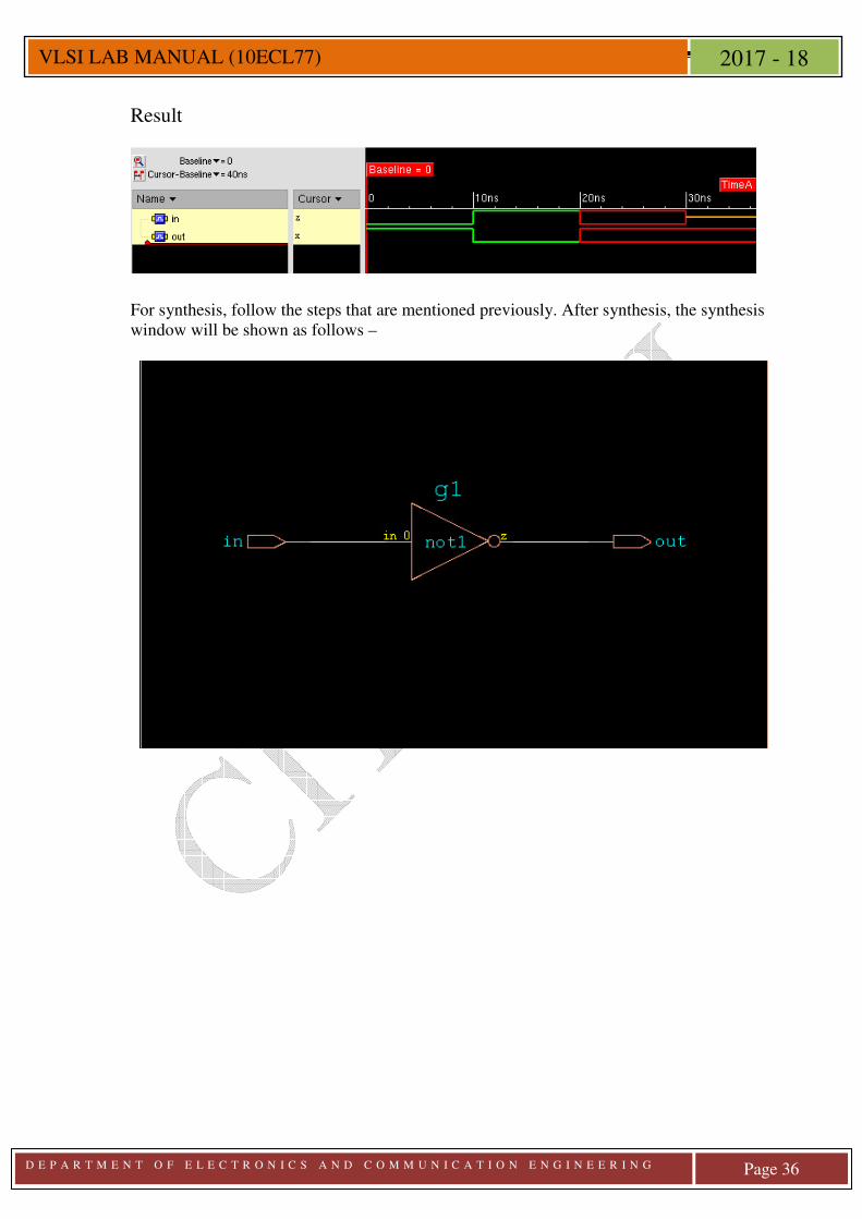
Result
For synthesis, follow the steps that are mentioned previously. After synthesis, the synthesis window will be shown as follows –
D E P A R T M E N T O F E L E C T R O N I C S A N D C O M M U N I C A T I O N E N G I N E E R I N G
Page 37
VLSI LAB MANUAL (10ECL77) 2017 - 18
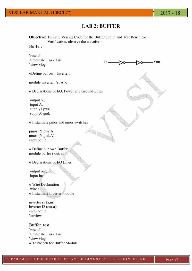
LAB 2: BUFFER Objective: To write Verilog Code for the Buffer circuit and Test Bench for Verification, observe the waveform. Buffer: `resetall `timescale 1 ns / 1 ns `view vlog //Define our own Inverter, module inverter( Y, A ); // Declarations of I/O, Power and Ground Lines output Y; input A; supply1 pwr; supply0 gnd; // Instantiate pmos and nmos switches pmos (Y,pwr,A); nmos (Y,gnd,A); endmodule // Define our own Buffer module buffer ( out, in ); // Declarations of I/O Lines output out; input in; // Wire Declaration wire a; // Instantiate Inverter module inverter i1 (a,in); inverter i2 (out,a); endmodule `noview
Buffer_test: `resetall `timescale 1 ns / 1 ns `view vlog // Testbench for Buffer Module
D E P A R T M E N T O F E L E C T R O N I C S A N D C O M M U N I C A T I O N E N G I N E E R I N G
Page 38
VLSI LAB MANUAL (10ECL77) 2017 - 18
module buf_test; wire out ; reg in ; `uselib view = vlog // Instantiate Buffer Module buffer b1( out,in ) ; `nouselib // Display task display ; begin $display ( "time=%0d" , $time , " ns", " Input=" , in , " Output=", out ) ; end endtask // Apply Stimulus initial begin in = 1'b0 ; #10 ; display ; in = 1'b1 ; #10 ; display ; in = 1'bx ; #10 ; display ; in = 1'bz ; #10 ; display ; end endmodule `noview
Constraints file for Synthesis: Constraints_Buffer.g set_input_delay -max 1.0 [get_ports "in"] set_output_delay -max 1.0 [get_ports "out"]
Truth Table
Input Output
A Y
0 0
1 1
X X
Z X
D E P A R T M E N T O F E L E C T R O N I C S A N D C O M M U N I C A T I O N E N G I N E E R I N G
Page 39
VLSI LAB MANUAL (10ECL77) 2017 - 18
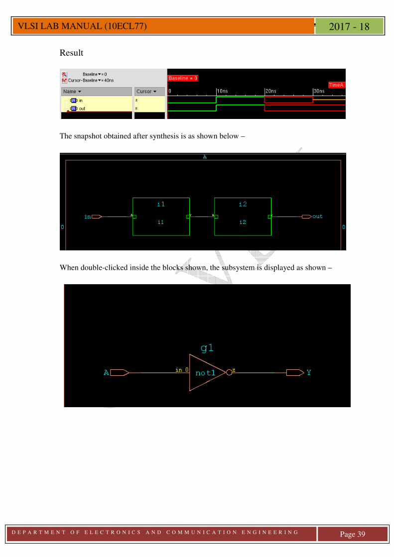
Result
The snapshot obtained after synthesis is as shown below –
When double-clicked inside the blocks shown, the subsystem is displayed as shown –
D E P A R T M E N T O F E L E C T R O N I C S A N D C O M M U N I C A T I O N E N G I N E E R I N G
Page 40
VLSI LAB MANUAL (10ECL77) 2017 - 18
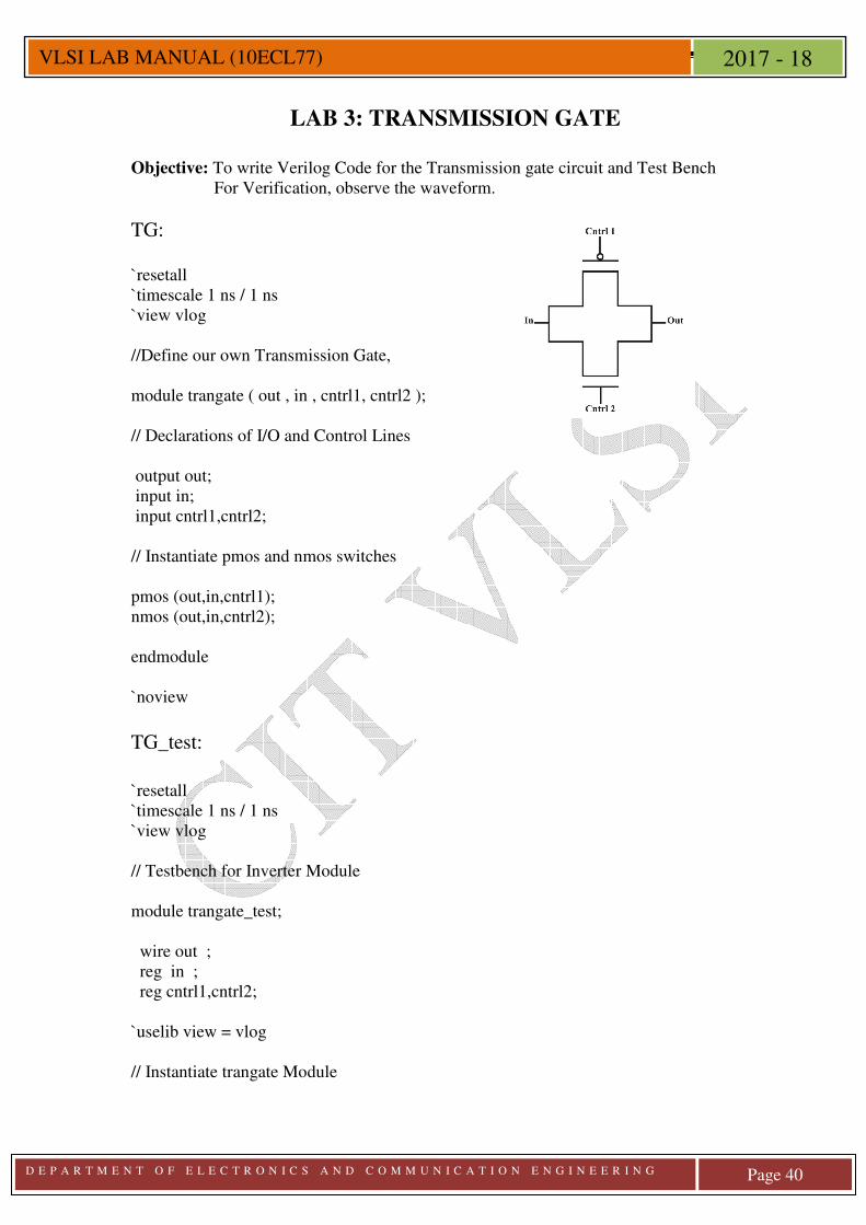
LAB 3: TRANSMISSION GATE Objective: To write Verilog Code for the Transmission gate circuit and Test Bench For Verification, observe the waveform.
TG: `resetall `timescale 1 ns / 1 ns `view vlog //Define our own Transmission Gate, module trangate ( out , in , cntrl1, cntrl2 ); // Declarations of I/O and Control Lines output out; input in; input cntrl1,cntrl2; // Instantiate pmos and nmos switches pmos (out,in,cntrl1); nmos (out,in,cntrl2); endmodule `noview
TG_test:
`resetall `timescale 1 ns / 1 ns `view vlog // Testbench for Inverter Module module trangate_test; wire out ; reg in ; reg cntrl1,cntrl2; `uselib view = vlog // Instantiate trangate Module
D E P A R T M E N T O F E L E C T R O N I C S A N D C O M M U N I C A T I O N E N G I N E E R I N G
Page 41
VLSI LAB MANUAL (10ECL77) 2017 - 18
trangate t1 ( out, in, cntrl1, cntrl2 ) ; `nouselib // Display task display ; begin $display ( "time=%0d" , $time , " ns", " Input=" , in, " Output=", out, " Control1=",cntrl1, " Control2=",cntrl2 ) ; end endtask // Apply Stimulus initial begin in = 1'b0 ; cntrl1 = 1'b0 ; cntrl2 = 1'b1 ; #10 ; display ; in = 1'b0 ; cntrl1 = 1'b1 ; cntrl2 = 1'b0 ; #10 ; display ; in = 1'b1 ; cntrl1 = 1'b0 ; cntrl2 = 1'b1 ; #10 ; display ; in = 1'b1 ; cntrl1 = 1'b1 ; cntrl2 = 1'b0 ; #10 ; display ; end endmodule `noview
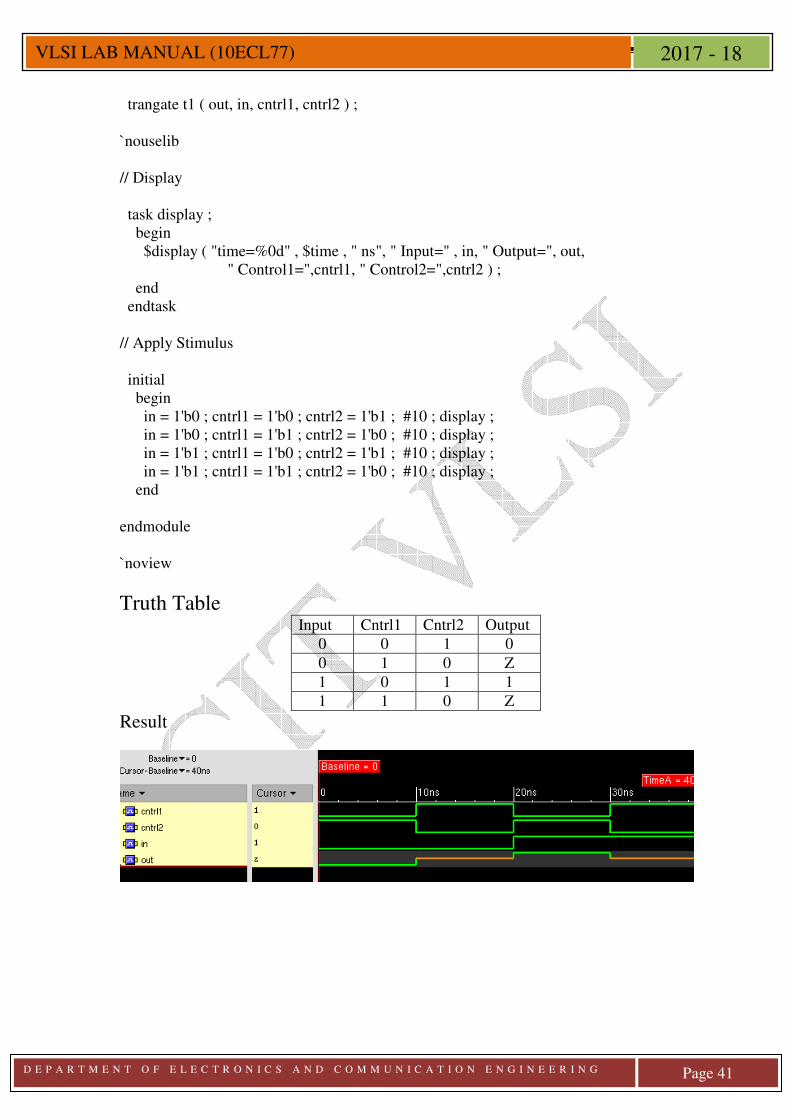
Truth Table Input Cntrl1 Cntrl2 Output
0 0 1 0
0 1 0 Z
1 0 1 1
1 1 0 Z
Result
D E P A R T M E N T O F E L E C T R O N I C S A N D C O M M U N I C A T I O N E N G I N E E R I N G
Page 42
VLSI LAB MANUAL (10ECL77) 2017 - 18
LAB 4: BASIC/ UNIVERSAL GATES
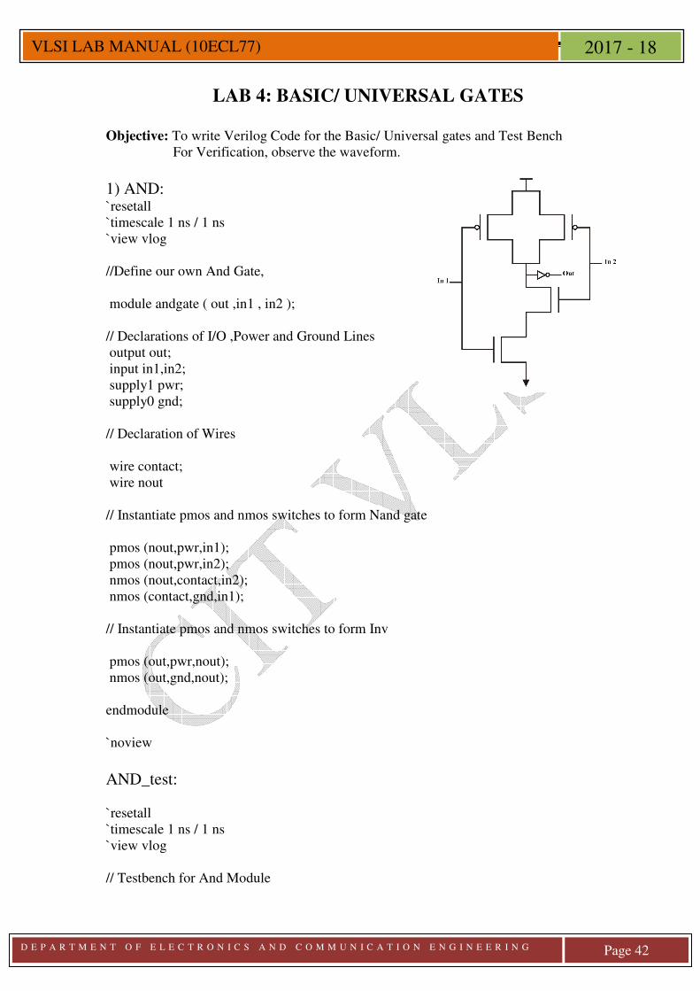
Objective: To write Verilog Code for the Basic/ Universal gates and Test Bench For Verification, observe the waveform.
1) AND: `resetall `timescale 1 ns / 1 ns `view vlog //Define our own And Gate, module andgate ( out ,in1 , in2 ); // Declarations of I/O ,Power and Ground Lines output out; input in1,in2; supply1 pwr; supply0 gnd; // Declaration of Wires wire contact; wire nout // Instantiate pmos and nmos switches to form Nand gate pmos (nout,pwr,in1); pmos (nout,pwr,in2); nmos (nout,contact,in2); nmos (contact,gnd,in1); // Instantiate pmos and nmos switches to form Inv pmos (out,pwr,nout); nmos (out,gnd,nout); endmodule `noview
AND_test: `resetall `timescale 1 ns / 1 ns `view vlog // Testbench for And Module
D E P A R T M E N T O F E L E C T R O N I C S A N D C O M M U N I C A T I O N E N G I N E E R I N G
Page 43
VLSI LAB MANUAL (10ECL77) 2017 - 18
module and_test; wire out ; reg in1,in2 ; `uselib view = vlog // Instantiate And Gate Module andgate a1 ( out, in1, in2 ) ; `nouselib // Display task display ; begin $display ( "time=%0d" , $time , " ns" ," Input1=" , in1 , " Input2=" , in2 , " Output=" , out ) ; end endtask // Apply Stimulus initial begin in1 = 1'b0 ; in2 = 1'b0 ; #10 ; display ; in1 = 1'b0 ; in2 = 1'b1 ; #10 ; display ; in1 = 1'b1 ; in2 = 1'b0 ; #10 ; display ; in1 = 1'b1 ; in2 = 1'b1 ; #10 ; display ; end endmodule `noview
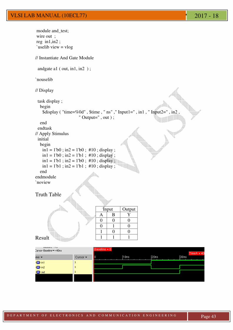
Truth Table
Result
Input Output
A B Y
0 0 0
0 1 0
1 0 0
1 1 1
D E P A R T M E N T O F E L E C T R O N I C S A N D C O M M U N I C A T I O N E N G I N E E R I N G
Page 44
VLSI LAB MANUAL (10ECL77) 2017 - 18
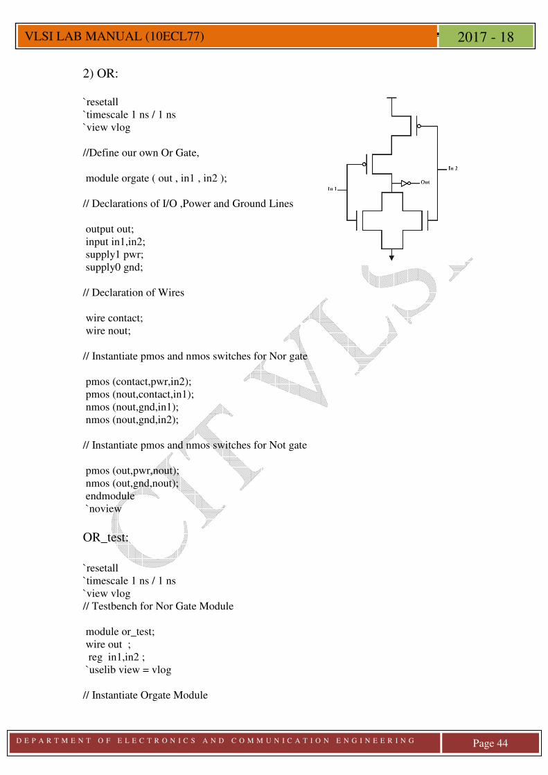
2) OR: `resetall `timescale 1 ns / 1 ns `view vlog //Define our own Or Gate, module orgate ( out , in1 , in2 ); // Declarations of I/O ,Power and Ground Lines output out; input in1,in2; supply1 pwr; supply0 gnd; // Declaration of Wires wire contact; wire nout; // Instantiate pmos and nmos switches for Nor gate pmos (contact,pwr,in2); pmos (nout,contact,in1); nmos (nout,gnd,in1); nmos (nout,gnd,in2); // Instantiate pmos and nmos switches for Not gate pmos (out,pwr,nout); nmos (out,gnd,nout); endmodule `noview
OR_test:
`resetall `timescale 1 ns / 1 ns `view vlog // Testbench for Nor Gate Module module or_test; wire out ; reg in1,in2 ; `uselib view = vlog // Instantiate Orgate Module
D E P A R T M E N T O F E L E C T R O N I C S A N D C O M M U N I C A T I O N E N G I N E E R I N G
Page 45
VLSI LAB MANUAL (10ECL77) 2017 - 18
orgate n1 ( out, in1, in2) ; `nouselib // Display task display ; begin $display ( "time=%0d" , $time , " ns" ," Input1=" , in1 , " Input2=" , in2 , " Output=" , out ) ; end endtask // Apply Stimulus initial begin in1 = 1'b0 ; in2 = 1'b0 ; #10 ; display ; in1 = 1'b0 ; in2 = 1'b1 ; #10 ; display ; in1 = 1'b1 ; in2 = 1'b0 ; #10 ; display ; in1 = 1'b1 ; in2 = 1'b1 ; #10 ; display ; end endmodule `noview
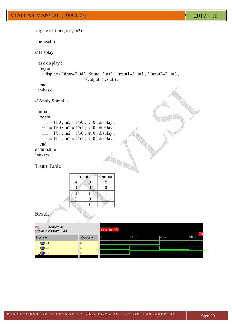
Truth Table
Result
Input Output
A B Y
0 0 0
0 1 1
1 0 1
1 1 1
D E P A R T M E N T O F E L E C T R O N I C S A N D C O M M U N I C A T I O N E N G I N E E R I N G
Page 46
VLSI LAB MANUAL (10ECL77) 2017 - 18
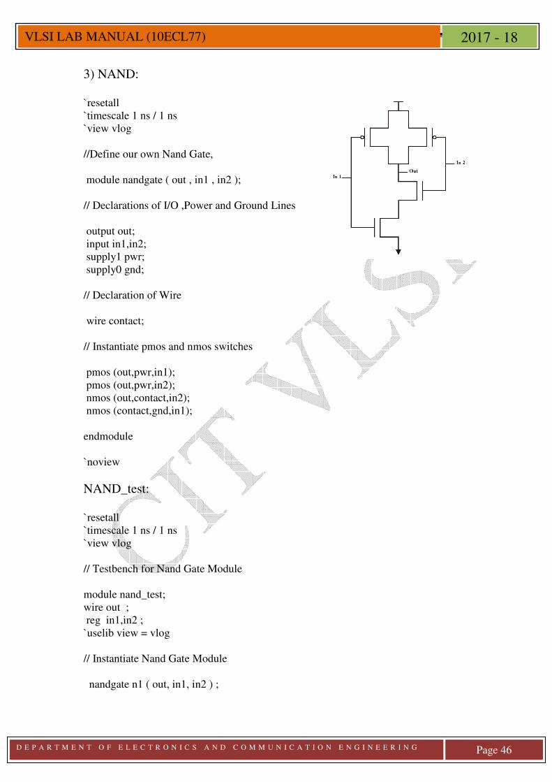
3) NAND: `resetall `timescale 1 ns / 1 ns `view vlog //Define our own Nand Gate, module nandgate ( out , in1 , in2 ); // Declarations of I/O ,Power and Ground Lines output out; input in1,in2; supply1 pwr; supply0 gnd; // Declaration of Wire wire contact; // Instantiate pmos and nmos switches pmos (out,pwr,in1); pmos (out,pwr,in2); nmos (out,contact,in2); nmos (contact,gnd,in1); endmodule `noview
NAND_test: `resetall `timescale 1 ns / 1 ns `view vlog // Testbench for Nand Gate Module module nand_test; wire out ; reg in1,in2 ; `uselib view = vlog // Instantiate Nand Gate Module nandgate n1 ( out, in1, in2 ) ;
D E P A R T M E N T O F E L E C T R O N I C S A N D C O M M U N I C A T I O N E N G I N E E R I N G
Page 47
VLSI LAB MANUAL (10ECL77) 2017 - 18
`nouselib // Display task display ; begin $display ( "time=%0d" , $time , " ns"," Input1=" , in1 , " Input2=" , in2 , " Output=" , out ) ; end endtask // Apply Stimulus initial begin in1 = 1'b0 ; in2 = 1'b0 ; #10 ; display ; in1 = 1'b0 ; in2 = 1'b1 ; #10 ; display ; in1 = 1'b1 ; in2 = 1'b0 ; #10 ; display ; in1 = 1'b1 ; in2 = 1'b1 ; #10 ; display ; end endmodule `noview
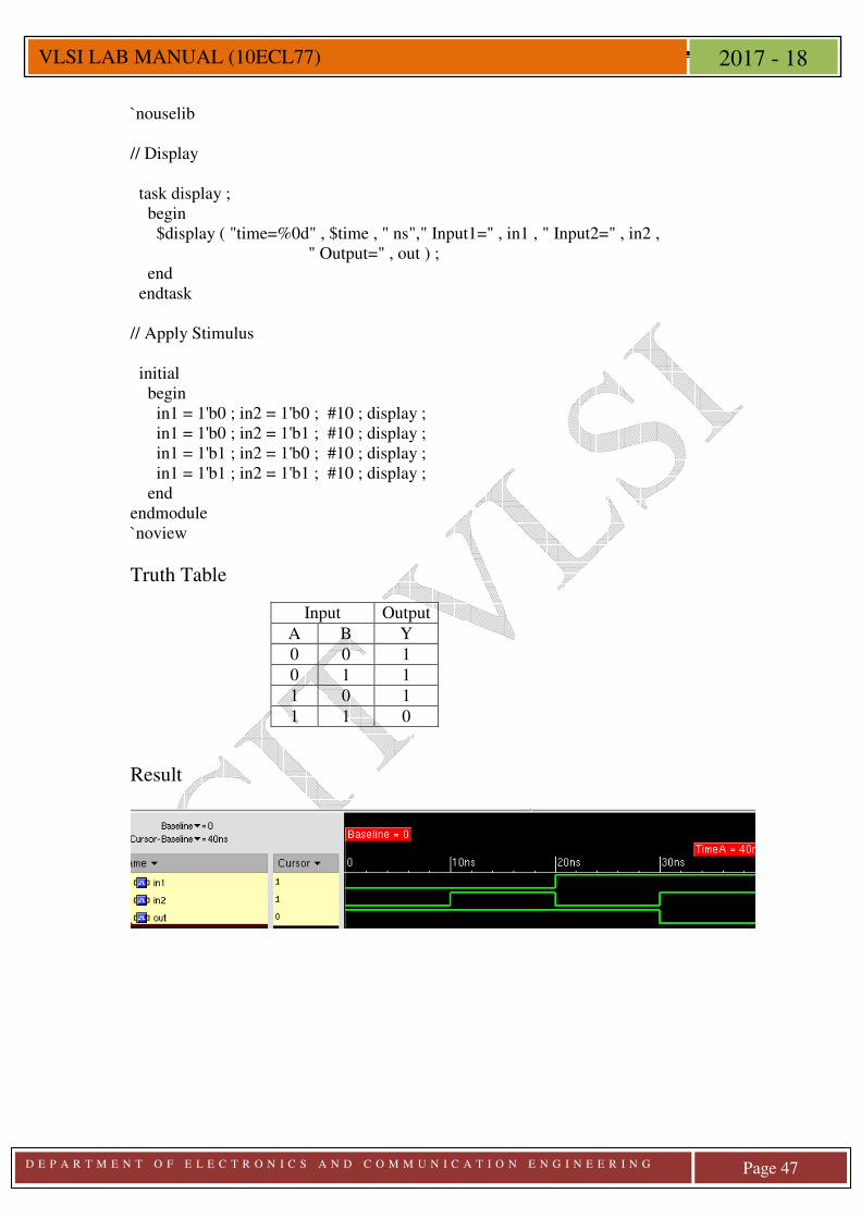
Truth Table
Result
Input Output
A B Y
0 0 1
0 1 1
1 0 1
1 1 0
D E P A R T M E N T O F E L E C T R O N I C S A N D C O M M U N I C A T I O N E N G I N E E R I N G
Page 48
VLSI LAB MANUAL (10ECL77) 2017 - 18
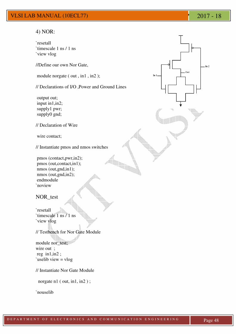
4) NOR: `resetall `timescale 1 ns / 1 ns `view vlog //Define our own Nor Gate, module norgate ( out , in1 , in2 ); // Declarations of I/O ,Power and Ground Lines output out; input in1,in2; supply1 pwr; supply0 gnd; // Declaration of Wire wire contact; // Instantiate pmos and nmos switches pmos (contact,pwr,in2); pmos (out,contact,in1); nmos (out,gnd,in1); nmos (out,gnd,in2); endmodule `noview
NOR_test
`resetall `timescale 1 ns / 1 ns `view vlog // Testbench for Nor Gate Module module nor_test; wire out ; reg in1,in2 ; `uselib view = vlog // Instantiate Nor Gate Module norgate n1 ( out, in1, in2 ) ; `nouselib
D E P A R T M E N T O F E L E C T R O N I C S A N D C O M M U N I C A T I O N E N G I N E E R I N G
Page 49
VLSI LAB MANUAL (10ECL77) 2017 - 18
// Display task display ; begin $display( "time=%0d" , $time , " ns" , " Input1=" , in1 , " Input2=" , in2 , " Output=" , out ) ; end endtask // Apply Stimulus initial begin in1 = 1'b0 ; in2 = 1'b0 ; #10 ; display ; in1 = 1'b0 ; in2 = 1'b1 ; #10 ; display ; in1 = 1'b1 ; in2 = 1'b0 ; #10 ; display ; in1 = 1'b1 ; in2 = 1'b1 ; #10 ; display ; end endmodule `noview
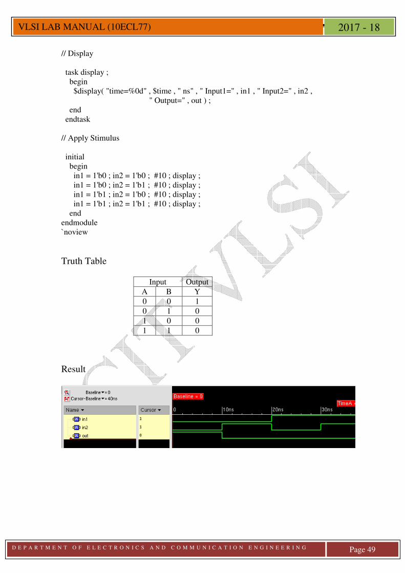
Truth Table
Result
Input Output
A B Y
0 0 1
0 1 0
1 0 0
1 1 0
D E P A R T M E N T O F E L E C T R O N I C S A N D C O M M U N I C A T I O N E N G I N E E R I N G
Page 50
VLSI LAB MANUAL (10ECL77) 2017 - 18
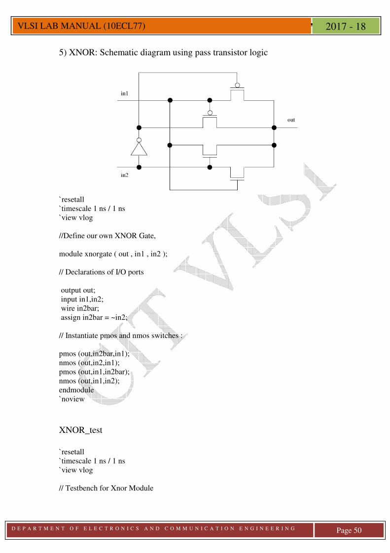
5) XNOR: Schematic diagram using pass transistor logic
`resetall `timescale 1 ns / 1 ns `view vlog //Define our own XNOR Gate, module xnorgate ( out , in1 , in2 ); // Declarations of I/O ports output out; input in1,in2; wire in2bar; assign in2bar = ~in2; // Instantiate pmos and nmos switches : pmos (out,in2bar,in1); nmos (out,in2,in1); pmos (out,in1,in2bar); nmos (out,in1,in2); endmodule `noview
XNOR_test
`resetall `timescale 1 ns / 1 ns `view vlog // Testbench for Xnor Module
D E P A R T M E N T O F E L E C T R O N I C S A N D C O M M U N I C A T I O N E N G I N E E R I N G
Page 51
VLSI LAB MANUAL (10ECL77) 2017 - 18
module xnor_test; wire out ; reg in1,in2 ; `uselib view = vlog // Instantiate Xnor gate Module xnorgate x1 ( out, in1, in2 ) ; `nouselib // Display task display ; begin $display ( "time=%0d" , $time , " ns"," Input1=" , in1 ," Input2=" , in2 , " Output=" , out ) ; end endtask // Apply Stimulus initial begin in1 = 1'b0 ; in2 = 1'b0 ; #10 ; display ; in1 = 1'b0 ; in2 = 1'b1 ; #10 ; display ; in1 = 1'b1 ; in2 = 1'b0 ; #10 ; display ; in1 = 1'b1 ; in2 = 1'b1 ; #10 ; display ; end endmodule `noview
Truth Table
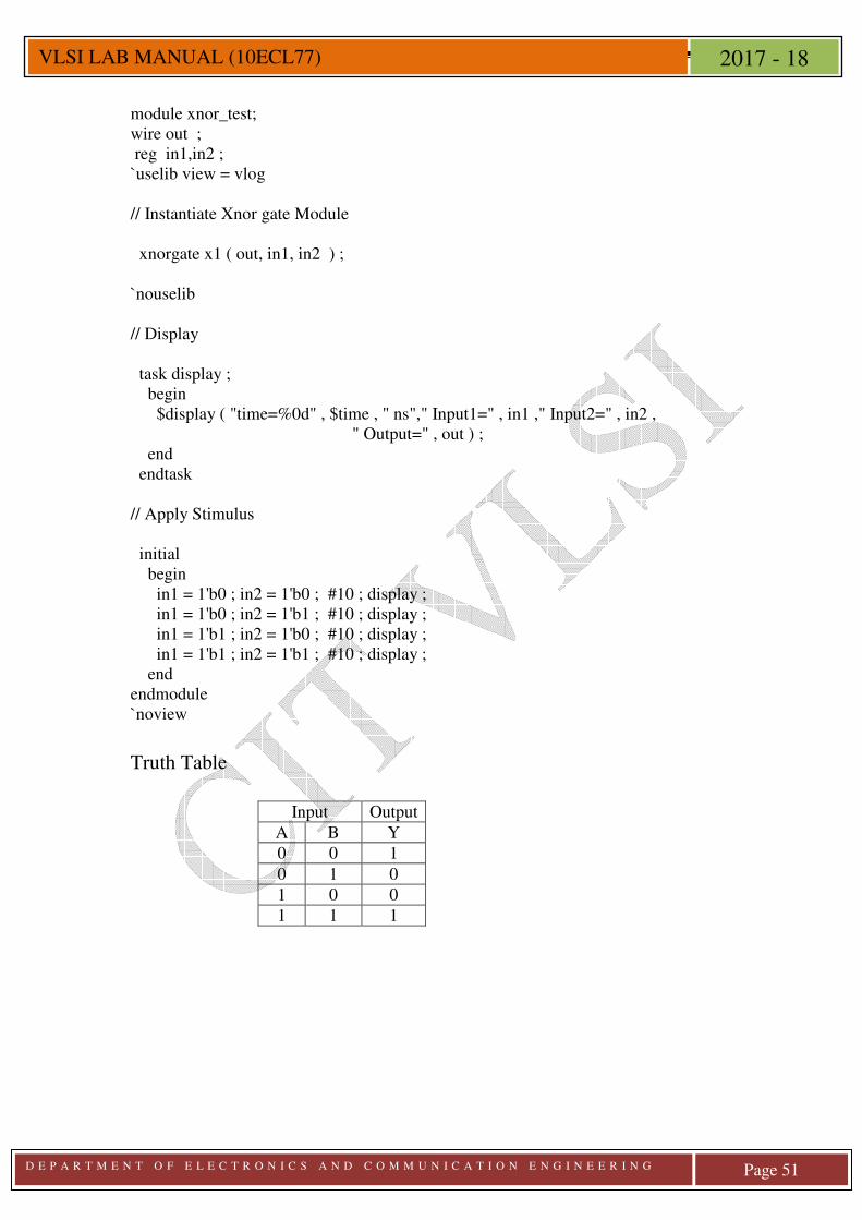
Input Output
A B Y
0 0 1
0 1 0
1 0 0
1 1 1
D E P A R T M E N T O F E L E C T R O N I C S A N D C O M M U N I C A T I O N E N G I N E E R I N G
Page 52
VLSI LAB MANUAL (10ECL77) 2017 - 18
Result
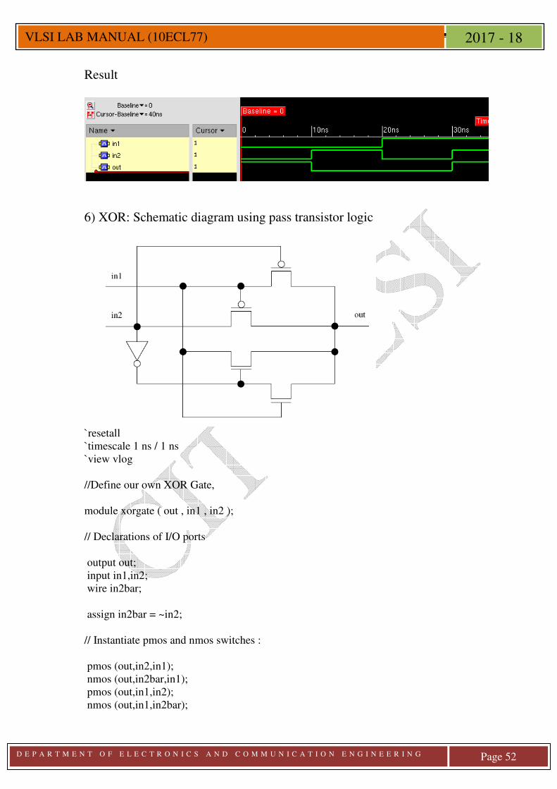
6) XOR: Schematic diagram using pass transistor logic
`resetall `timescale 1 ns / 1 ns `view vlog //Define our own XOR Gate, module xorgate ( out , in1 , in2 ); // Declarations of I/O ports output out; input in1,in2; wire in2bar; assign in2bar = ~in2; // Instantiate pmos and nmos switches : pmos (out,in2,in1); nmos (out,in2bar,in1); pmos (out,in1,in2); nmos (out,in1,in2bar);
D E P A R T M E N T O F E L E C T R O N I C S A N D C O M M U N I C A T I O N E N G I N E E R I N G
Page 53
VLSI LAB MANUAL (10ECL77) 2017 - 18
endmodule `noview
XOR_test:
`resetall `timescale 1 ns / 1 ns `view vlog // Testbench for Xor Module module xor_test; wire out ; reg in1,in2 ; `uselib view = vlog // Instantiate Xorgate Module xorgate x1 ( out, in1, in2 ) ; `nouselib // Display task display ; begin $display( "time=%0d" , $time , " ns" , " Input1=" , in1," Input2=" , in2, " Output=" , out ) ; end endtask // Apply Stimulus initial begin in1 = 1'b0 ; in2 = 1'b0 ; #10 ; display ; in1 = 1'b0 ; in2 = 1'b1 ; #10 ; display ; in1 = 1'b1 ; in2 = 1'b0 ; #10 ; display ; in1 = 1'b1 ; in2 = 1'b1 ; #10 ; display ; end endmodule `noview
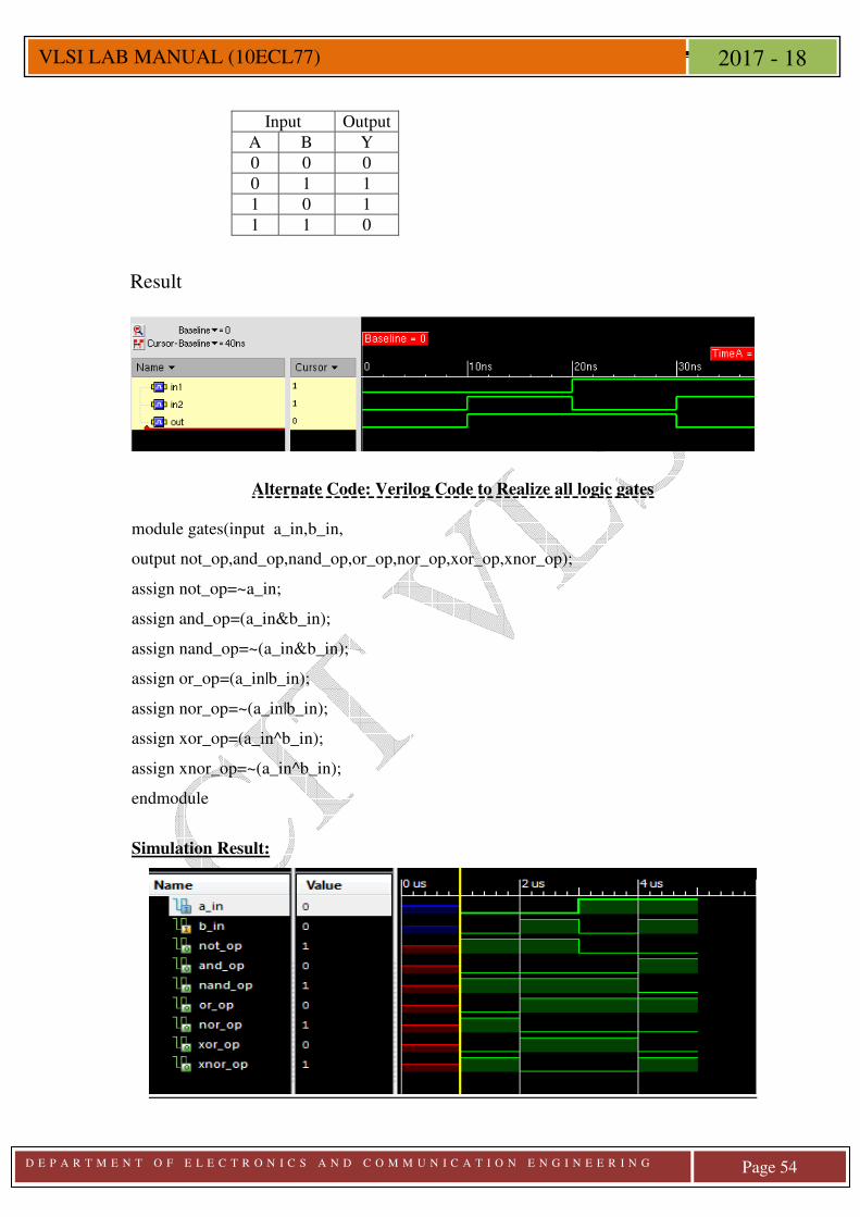
Truth Table
D E P A R T M E N T O F E L E C T R O N I C S A N D C O M M U N I C A T I O N E N G I N E E R I N G
Page 54
VLSI LAB MANUAL (10ECL77) 2017 - 18
Result
Alternate Code: Verilog Code to Realize all logic gates
module gates(input a_in,b_in,
output not_op,and_op,nand_op,or_op,nor_op,xor_op,xnor_op);
assign not_op=~a_in;
assign and_op=(a_in&b_in);
assign nand_op=~(a_in&b_in);
assign or_op=(a_in|b_in);
assign nor_op=~(a_in|b_in);
assign xor_op=(a_in^b_in);
assign xnor_op=~(a_in^b_in);
endmodule
Simulation Result:
Input Output
A B Y
0 0 0
0 1 1
1 0 1
1 1 0
D E P A R T M E N T O F E L E C T R O N I C S A N D C O M M U N I C A T I O N E N G I N E E R I N G
Page 55
VLSI LAB MANUAL (10ECL77) 2017 - 18
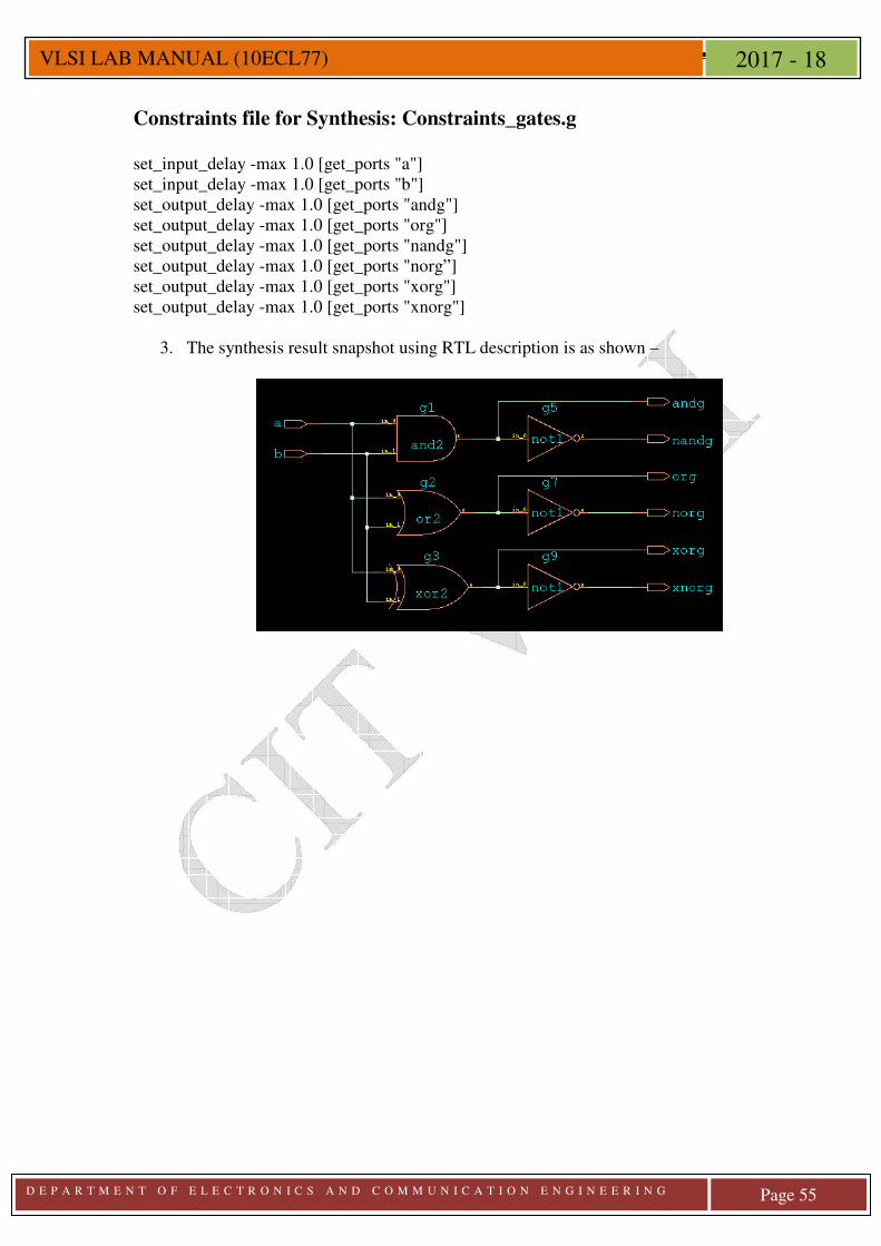
Constraints file for Synthesis: Constraints_gates.g set_input_delay -max 1.0 [get_ports "a"] set_input_delay -max 1.0 [get_ports "b"] set_output_delay -max 1.0 [get_ports "andg"] set_output_delay -max 1.0 [get_ports "org"] set_output_delay -max 1.0 [get_ports "nandg"] set_output_delay -max 1.0 [get_ports "norg”] set_output_delay -max 1.0 [get_ports "xorg"] set_output_delay -max 1.0 [get_ports "xnorg"]
3. The synthesis result snapshot using RTL description is as shown –
D E P A R T M E N T O F E L E C T R O N I C S A N D C O M M U N I C A T I O N E N G I N E E R I N G
Page 56
VLSI LAB MANUAL (10ECL77) 2017 - 18
LAB 5: FLIP FLOPS
Objective: To write Verilog Code for various Flip flop circuits and Test Bench For Verification, observe the waveform.
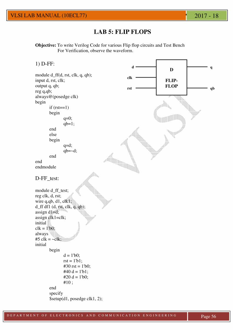
1) D-FF: module d_ff(d, rst, clk, q, qb); input d, rst, clk; output q, qb; reg q,qb; always@(posedge clk) begin
if (rst==1) begin
q=0; qb=1;
end else begin
q=d; qb=~d;
end end endmodule
D-FF_test: module d_ff_test; reg clk, d, rst; wire q,qb, d1, clk1; d_ff df1 (d, rst, clk, q, qb); assign d1=d; assign clk1=clk; initial clk = 1'b0; always #5 clk = ~clk; initial begin d = 1'b0; rst = 1'b1; #30 rst = 1'b0; #40 d = 1'b1; #20 d = 1'b0; #10 ; end specify $setup(d1, posedge clk1, 2);
D
FLIP-FLOP
d
clk
rst
q
qb
D E P A R T M E N T O F E L E C T R O N I C S A N D C O M M U N I C A T I O N E N G I N E E R I N G
Page 57
VLSI LAB MANUAL (10ECL77) 2017 - 18
$hold(posedge clk1, d1, 2); $width(negedge d1, 2); endspecify endmodule
Truth Table
RESET D Q QBAR 1 X 0 1
0 0 0 1
0 1 1 0
Result
2) JK-ff: module jk_ff(jk, clk, rst, q, qb); input [1:0]jk; input clk,rst; output q, qb; reg q, qb; always @ (posedge clk) begin
if(rst==1) begin
q=0; qb=1;
end else begin
case (jk) 2'b00: begin q=q; qb=qb; end 2'b01: begin q=0; qb=1; end 2'b10: begin q=1; qb=0; end 2'b11: begin q=~(q); qb=~(qb); end
endcase end
end endmodule
JK-FF_test:
D E P A R T M E N T O F E L E C T R O N I C S A N D C O M M U N I C A T I O N E N G I N E E R I N G
Page 58
VLSI LAB MANUAL (10ECL77) 2017 - 18
module jk_ff_test; reg clk,rst; reg [1:0] jk; wire q,qb; wire clk1; wire [1:0] jk1; jk_ff jkff(jk, clk, rst, q, qb); assign clk1=clk; assign jk1=jk; initial clk = 1'b0; always #5 clk = ~clk; initial begin jk = 2'b00; rst = 1'b1; #20 rst = 1'b0; #20 jk = 2'b01; #20 jk = 2'b10; #20 jk = 2'b11; #20 rst = 1'b1; #10 ; end specify $setup(j1, posedge clk1, 2);
$setup(k1, posedge clk1, 2);
$hold(posedge clk1, j1, 2);
$hold(posedge clk1, k1, 2);
endspecify
endmodule
Constraints file for Synthesis: Constraints_JK_ff.g create_clock -name clk -period 10 -waveform {0 5} [get_ports "clk"]
set_clock_transition -rise 0.1 [get_clocks "clk"]
set_clock_transition -fall 0.1 [get_clocks "clk"]
set_clock_uncertainty 1.0 [get_ports "clk"]
set_input_delay -max 1.0 [get_ports "rst"] -clock [get_clocks "clk"]
set_input_delay -max 1.0 [get_ports "j"] -clock [get_clocks "clk"]
set_input_delay -max 1.0 [get_ports "k"] -clock [get_clocks "clk"]
set_output_delay -max 1.0 [get_ports "q"] -clock [get_clocks "clk"]
set_output_delay -max 1.0 [get_ports "qbar"] -clock [get_clocks "clk"]
D E P A R T M E N T O F E L E C T R O N I C S A N D C O M M U N I C A T I O N E N G I N E E R I N G
Page 59
VLSI LAB MANUAL (10ECL77) 2017 - 18
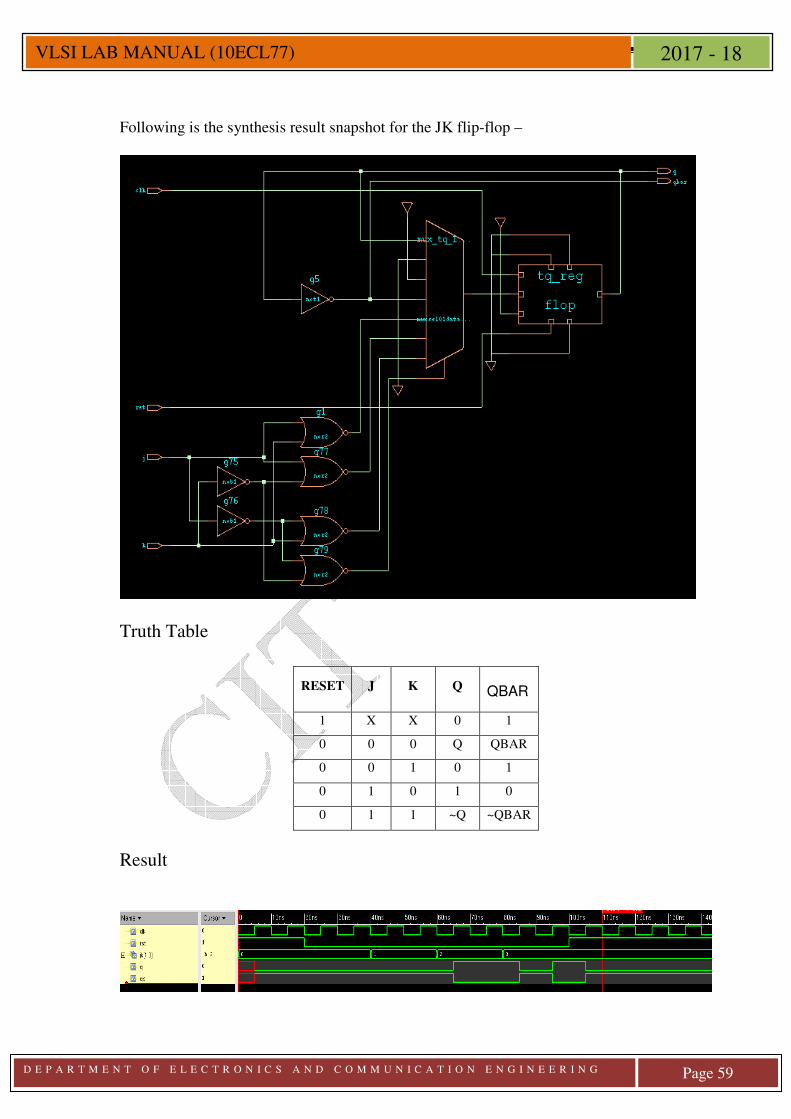
Following is the synthesis result snapshot for the JK flip-flop –
Truth Table
RESET J K Q QBAR
1 X X 0 1
0 0 0 Q QBAR
0 0 1 0 1
0 1 0 1 0
0 1 1 ~Q ~QBAR
Result
D E P A R T M E N T O F E L E C T R O N I C S A N D C O M M U N I C A T I O N E N G I N E E R I N G
Page 60
VLSI LAB MANUAL (10ECL77) 2017 - 18
3) MS-FF: module ms_jkff(q,q_bar,clk,j,k); output q,q_bar; input clk,j,k; reg tq,q,q_bar; always @(clk) begin if (!clk) begin if (j==1'b0 && k==1'b1) tq <= 1'b0; else if (j==1'b1 && k==1'b0) tq <= 1'b1; else if (j==1'b1 && k==1'b1) tq <= ~tq; end if (clk) begin q <= tq; q_bar <= ~tq; end end endmodule
MS-FF_test: module tb_ms_jkff; reg clk,j,k; wire q,q_bar; wire clk2,j2,k2; ms_jkff inst(q,q_bar,clk,j,k); assign clk2=clk; assign j2=j; assign k2=k; initial clk = 1'b0; always #10 clk = ~clk; initial begin j = 1'b0; k = 1'b0; #60 j = 1'b0; k = 1'b1; #40 j = 1'b1; k = 1'b0; #20 j = 1'b1; k = 1'b1; #40 j = 1'b1; k = 1'b0; #5 j = 1'b0; #20 j = 1'b1; #10 ; end
D E P A R T M E N T O F E L E C T R O N I C S A N D C O M M U N I C A T I O N E N G I N E E R I N G
Page 61
VLSI LAB MANUAL (10ECL77) 2017 - 18
always #5 $display($time," clk=%b j=%b k=%b ",clk,j,k); initial #200 $finish; specify $setup(j2, posedge clk2, 2); $setup(k2, posedge clk2, 2); $hold(posedge clk2, j2, 2); $hold(posedge clk2, k2, 2); endspecify endmodule
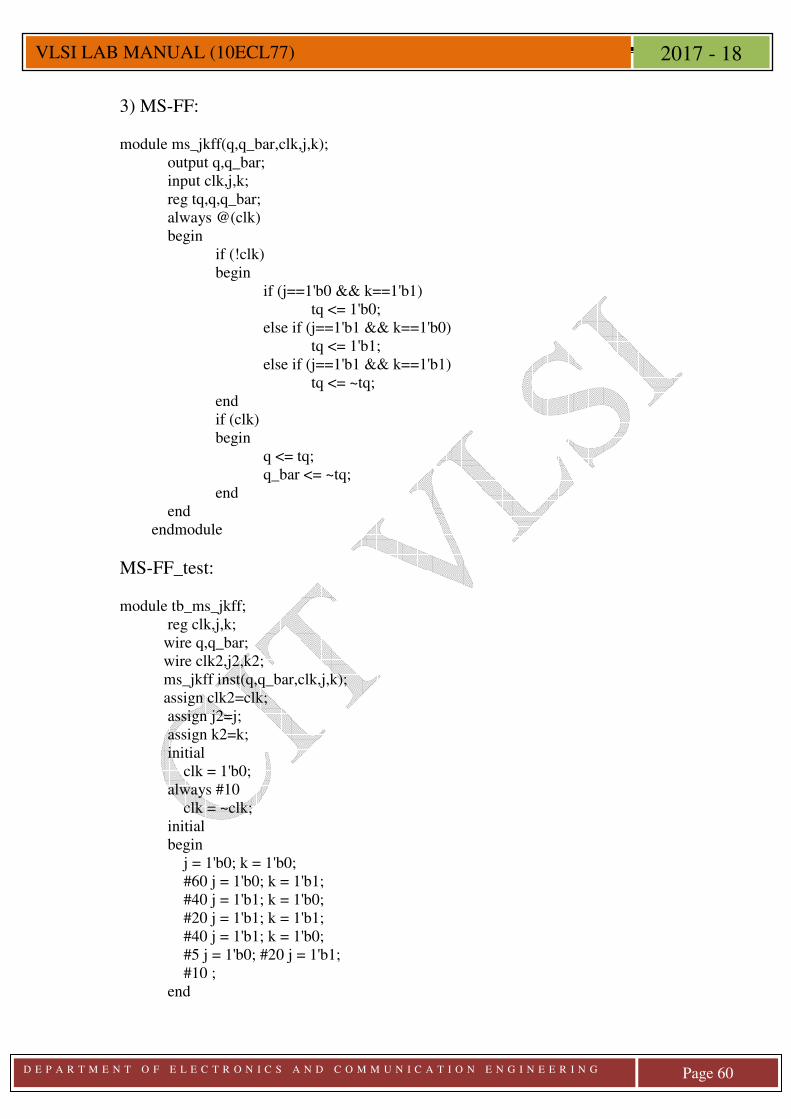
Truth Table
RESET J K Q QBAR
0 X X 0 1
1 0 0 0 1
1 0 1 0 1
1 1 0 1 0
1 1 1 1 0
Result
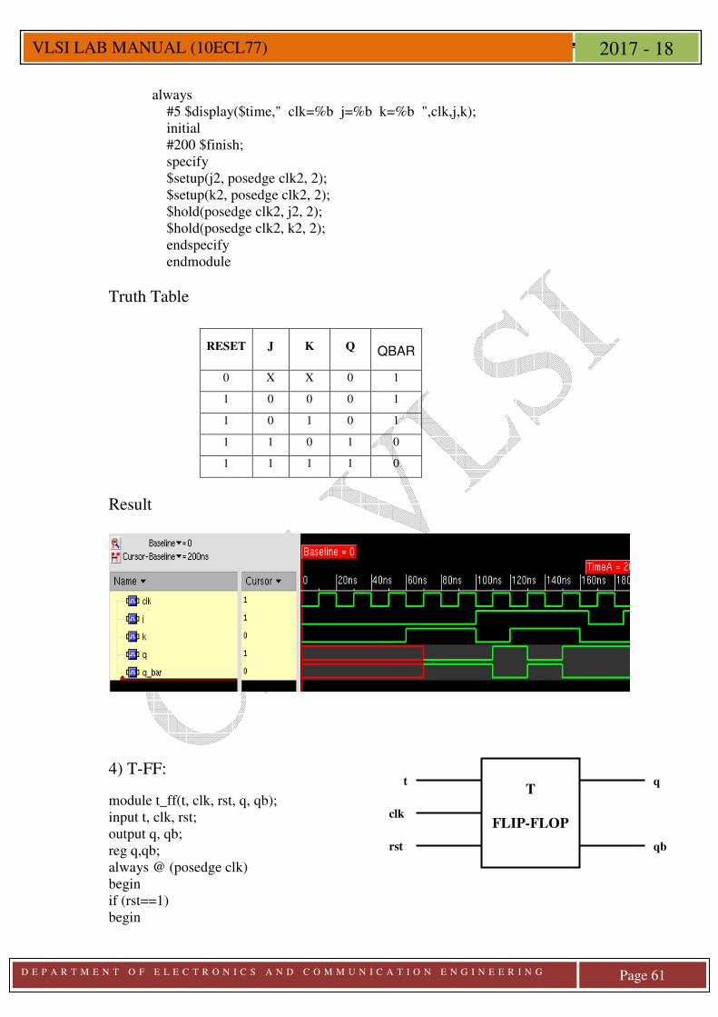
4) T-FF:
module t_ff(t, clk, rst, q, qb); input t, clk, rst; output q, qb; reg q,qb; always @ (posedge clk) begin if (rst==1) begin
T
FLIP-FLOP
t
clk
rst
q
qb
D E P A R T M E N T O F E L E C T R O N I C S A N D C O M M U N I C A T I O N E N G I N E E R I N G
Page 62
VLSI LAB MANUAL (10ECL77) 2017 - 18
q=1’b0; qb=1’b1;
end else begin
case t 1’b0:begin q=q; qb=qb; end 1’b1:begin q=~(q); qb=~(qb); end
endcase end end endmodule
T-FF_test:
module t_ff_t; reg clk,t,rst; wire q,qb; t_ff t1(t, clk, rst, q, qb); initial clk = 1'b0; always #10 clk = ~clk; initial begin rst = 1'b1; t = 1'b0; #30 rst = 1'b0; #10 t = 1'b1; #30 t = 1'b0; #20 rst = 1'b1; #20 ; end endmodule
Truth Table
RESET T Q QBAR
1 X 0 1
0 0 Q QBAR
0 1 ~Q ~QBAR
D E P A R T M E N T O F E L E C T R O N I C S A N D C O M M U N I C A T I O N E N G I N E E R I N G
Page 63
VLSI LAB MANUAL (10ECL77) 2017 - 18
Result
5) RS-FF: module sr_ff(sr, clk, rst, q, qb); input [1:0] sr; input rst, clk; output q,qb; reg q,qb; always @ (posedge clk) begin if (rst==1) begin q=0; qb=1; end else begin case (sr) 2'b00: begin q=q; qb=qb; end 2'b01: begin q=0; qb=1; end 2'b10: begin q=1; qb=0; end 2'b11: begin q=1'bx; qb=1'bx; end endcase end end endmodule
RS-FF_test: module sr_ff_test; reg clk,rst; wire q,qb; reg [1:0] sr; wire [1:0] sr1;
wire clk1; sr_ff sr1(sr, clk, rst, q, qb); assign sr1=sr; assign clk1=clk; initial clk = 1'b0; always
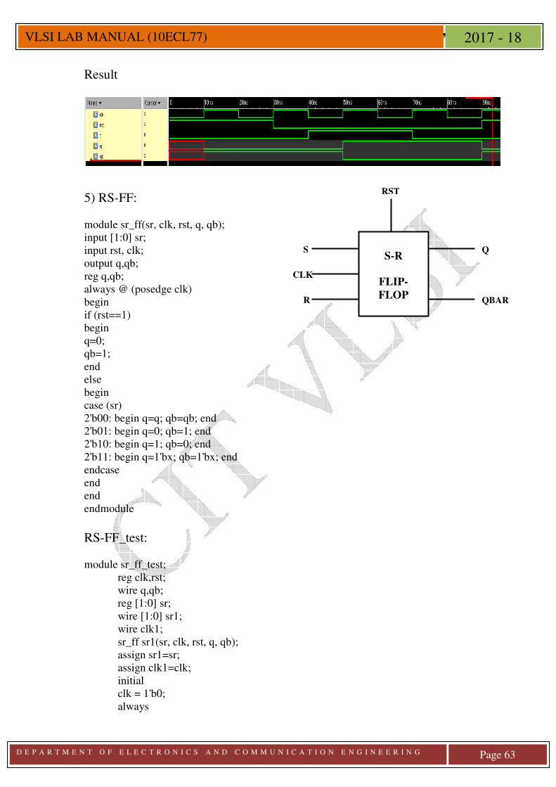
S-R
FLIP-FLOP
S
CLK
R
Q
QBAR
RST
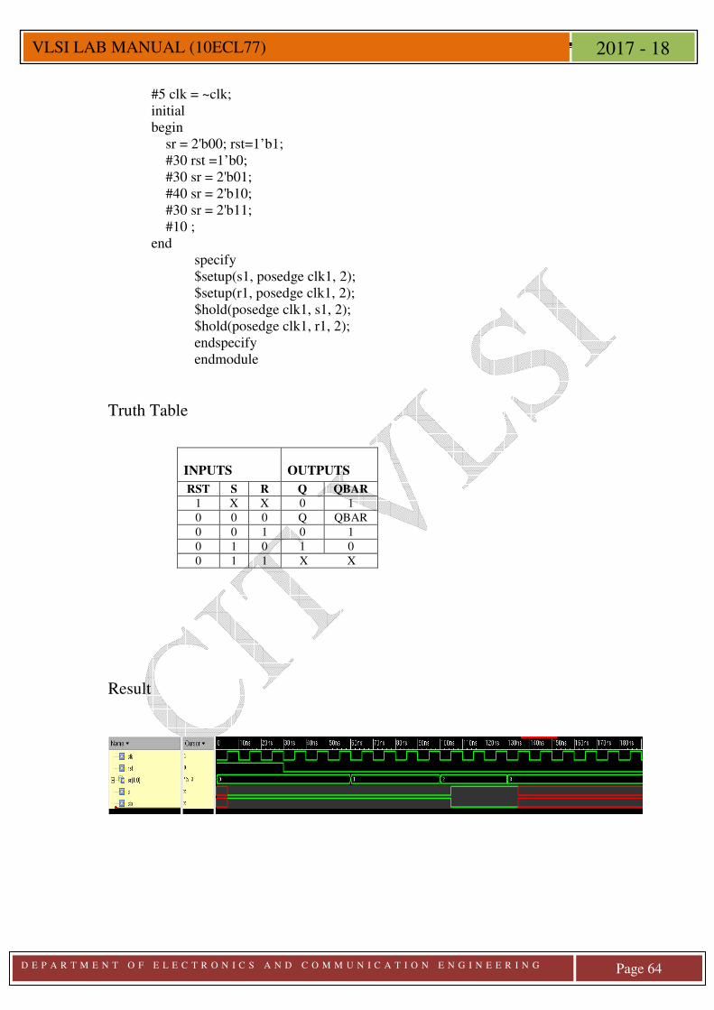
D E P A R T M E N T O F E L E C T R O N I C S A N D C O M M U N I C A T I O N E N G I N E E R I N G
Page 64
VLSI LAB MANUAL (10ECL77) 2017 - 18
#5 clk = ~clk; initial begin sr = 2'b00; rst=1’b1; #30 rst =1’b0; #30 sr = 2'b01; #40 sr = 2'b10; #30 sr = 2'b11; #10 ; end specify $setup(s1, posedge clk1, 2); $setup(r1, posedge clk1, 2); $hold(posedge clk1, s1, 2); $hold(posedge clk1, r1, 2); endspecify endmodule
Truth Table
INPUTS OUTPUTS
RST S R Q QBAR 1 X X 0 1
0 0 0 Q QBAR
0 0 1 0 1
0 1 0 1 0
0 1 1 X X
Result
D E P A R T M E N T O F E L E C T R O N I C S A N D C O M M U N I C A T I O N E N G I N E E R I N G
Page 65
VLSI LAB MANUAL (10ECL77) 2017 - 18
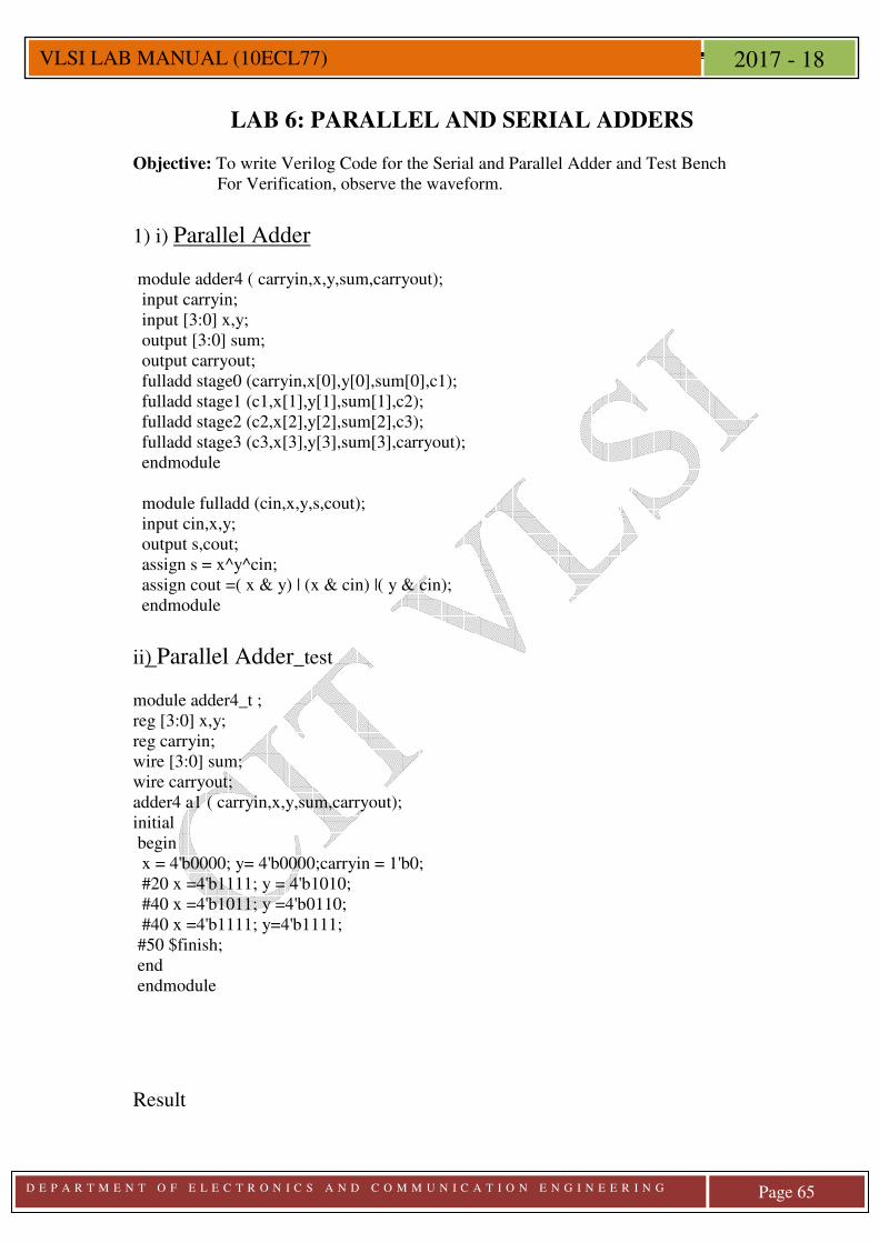
LAB 6: PARALLEL AND SERIAL ADDERS Objective: To write Verilog Code for the Serial and Parallel Adder and Test Bench For Verification, observe the waveform.
1) i) Parallel Adder module adder4 ( carryin,x,y,sum,carryout); input carryin; input [3:0] x,y; output [3:0] sum; output carryout; fulladd stage0 (carryin,x[0],y[0],sum[0],c1); fulladd stage1 (c1,x[1],y[1],sum[1],c2); fulladd stage2 (c2,x[2],y[2],sum[2],c3); fulladd stage3 (c3,x[3],y[3],sum[3],carryout); endmodule module fulladd (cin,x,y,s,cout); input cin,x,y; output s,cout; assign s = x^y^cin; assign cout =( x & y) | (x & cin) |( y & cin); endmodule
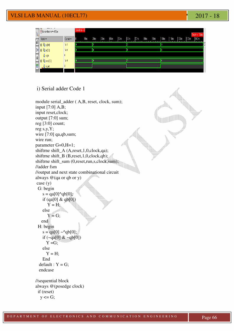
ii) Parallel Adder_test module adder4_t ; reg [3:0] x,y; reg carryin; wire [3:0] sum; wire carryout; adder4 a1 ( carryin,x,y,sum,carryout); initial begin x = 4'b0000; y= 4'b0000;carryin = 1'b0; #20 x =4'b1111; y = 4'b1010; #40 x =4'b1011; y =4'b0110; #40 x =4'b1111; y=4'b1111; #50 $finish; end endmodule
Result
D E P A R T M E N T O F E L E C T R O N I C S A N D C O M M U N I C A T I O N E N G I N E E R I N G
Page 66
VLSI LAB MANUAL (10ECL77) 2017 - 18
i) Serial adder Code 1
module serial_adder ( A,B, reset, clock, sum); input [7:0] A,B; input reset,clock; output [7:0] sum; reg [3:0] count; reg s,y,Y; wire [7:0] qa,qb,sum; wire run; parameter G=0,H=1; shiftrne shift_A (A,reset,1,0,clock,qa); shiftrne shift_B (B,reset,1,0,clock,qb); shiftrne shift_sum (0,reset,run,s,clock,sum); //adder fsm //output and next state combinational circuit always @(qa or qb or y) case (y) G: begin s = qa[0]^qb[0]; if (qa[0] & qb[0]) Y = H; else Y = G; end H: begin s = qa[0] ~^qb[0]; if (~qa[0] & ~qb[0]) Y =G; else Y = H; End default : Y = G; endcase //sequential block always @(posedge clock) if (reset) y <= G;
D E P A R T M E N T O F E L E C T R O N I C S A N D C O M M U N I C A T I O N E N G I N E E R I N G
Page 67
VLSI LAB MANUAL (10ECL77) 2017 - 18
else y <= Y; //control the shifting process always @(posedge clock) if (reset) count = 8; else if (run) count = count - 1; assign run=|count; endmodule
ii) Serial adder_test
module serial_adder_t ; reg [7:0] A,B; reg reset,clock; wire [7:0] sum ; initial clock = 1'b0; always #5 clock =~clock; serial_adder s1 (A,B,reset,clock,sum); initial begin reset = 1'b0;A = 8'b10101010; B = 8'b11111111; #20 reset = 1'b1; #20 reset = 1'b0; #150 reset = 1'b1; A = 11110000 ; B = 8'b11110011; #20 reset = 1'b0; #200 $finish; end initial $monitor ($time, " SUM = %d ", sum); endmodule iii) Shift reg:
module shiftrne ( R,L,E,w,clock,q); parameter n=8; input [n-1:0] R; input L,E,w,clock; output [n-1:0] q; reg [n-1:0] q; integer k; always @(posedge clock) if (L) q <= R; else if (E)
D E P A R T M E N T O F E L E C T R O N I C S A N D C O M M U N I C A T I O N E N G I N E E R I N G
Page 68
VLSI LAB MANUAL (10ECL77) 2017 - 18
begin for (k=n-1;k>0;k=k-1) q[k-1] <= q[k]; q[n-1] <= w; end endmodule
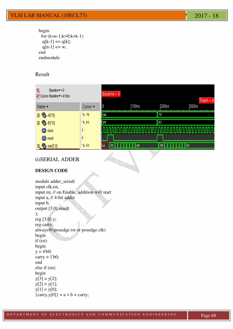
Result
ii)SERIAL ADDER DESIGN CODE module adder_serial( input clk,rst, input en, // on Enable, addition will start input a, // 4-bit adder input b, output [3:0] result ); reg [3:0] y; reg carry; always@(posedge rst or posedge clk) begin if (rst) begin y = 4'b0; carry = 1'b0; end else if (en) begin y[3] = y[2]; y[2] = y[1]; y[1] = y[0]; {carry,y[0]} = a + b + carry;
D E P A R T M E N T O F E L E C T R O N I C S A N D C O M M U N I C A T I O N E N G I N E E R I N G
Page 69
VLSI LAB MANUAL (10ECL77) 2017 - 18
end end assign result = y; endmodule TEST BENCH CODE module serial_adder_test;
reg clk,rst,en,a,b;
Wire [3:0] result;
adder_serial U1 (clk,rst,en,a,b,result); //instantiation
Initial
clk=1’b0;
always
#5 clk=~clk;
Initial
begin
Rst =1’b1;en=1’b0;a=0;b=0;
#10 Rst =1’b0;en=1’b1;a=1;b=0;
#10 Rst =1’b0;en=1’b1;a=0;b=1;
#10 Rst =1’b0;en=1’b1;a=1;b=1;
#10 Rst =1’b0;en=1’b1;a=0;b=1;
#10 Rst =1’b0;en=1’b1;a=1;b=0;
#200 $finish;
end
endmodule
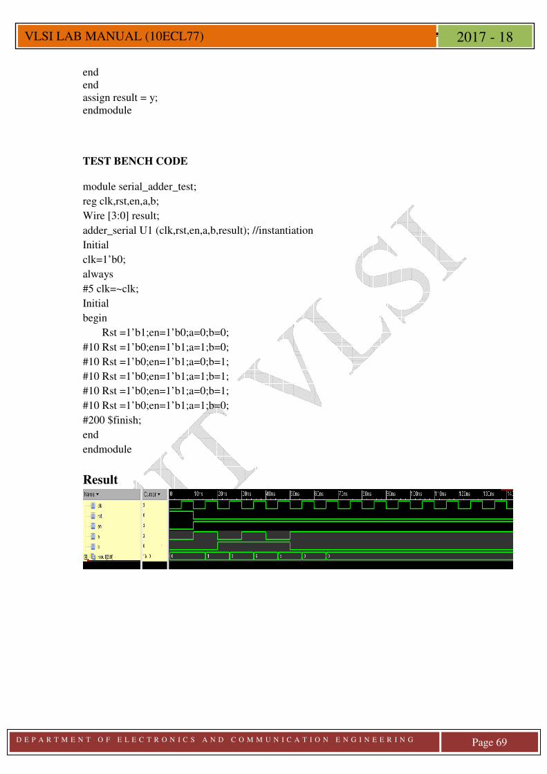
Result
D E P A R T M E N T O F E L E C T R O N I C S A N D C O M M U N I C A T I O N E N G I N E E R I N G
Page 70
VLSI LAB MANUAL (10ECL77) 2017 - 18
LAB 7: 4-BIT COUNTERS Objective: To write Verilog Code for the 4-bit Synchronous and Asynchronous counter And Test Bench for Verification, observe the waveform.
1) Asynchronous counter: module counter_behav ( count,reset,clk); input wire reset, clk; output reg [3:0] count; always @(posedge clk or posedge rst) begin if (reset) count <= 4'b0000; else count <= count + 4'b0001; end endmodule
Asynchronous counter_test
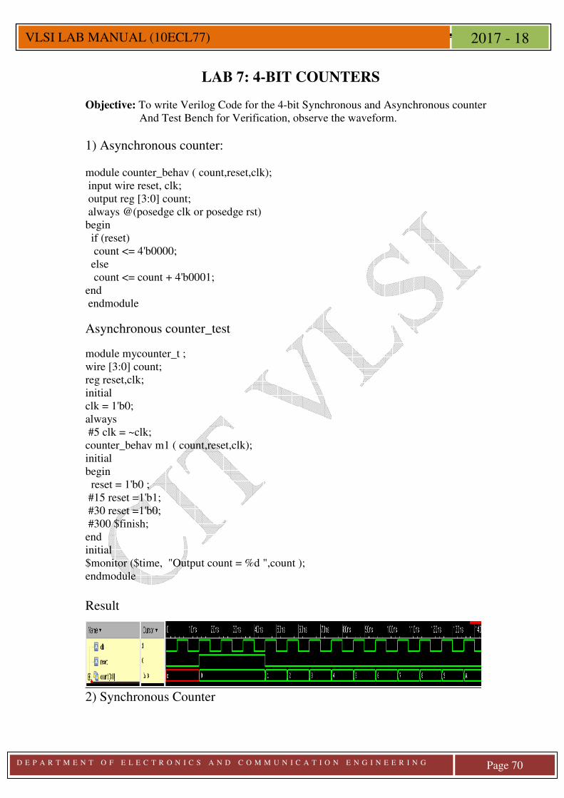
module mycounter_t ; wire [3:0] count; reg reset,clk; initial clk = 1'b0; always #5 clk = ~clk; counter_behav m1 ( count,reset,clk); initial begin reset = 1'b0 ; #15 reset =1'b1; #30 reset =1'b0; #300 $finish; end initial $monitor ($time, "Output count = %d ",count ); endmodule
Result
2) Synchronous Counter
D E P A R T M E N T O F E L E C T R O N I C S A N D C O M M U N I C A T I O N E N G I N E E R I N G
Page 71
VLSI LAB MANUAL (10ECL77) 2017 - 18
module counter_behav ( count,reset,clk); input wire reset, clk; output reg [3:0] count; initial count =4’b0000; always @(posedge clk) if (reset) count <= 4'b0000; else count <= count + 4'b0001; endmodule
Synchronous counter_test module mycounter_t ; wire [3:0] count; reg reset,clk; initial clk = 1'b0; always #5 clk = ~clk; counter_behav m1 ( count,reset,clk); initial begin reset = 1'b0 ; #15 reset =1'b1; #30 reset =1'b0; #300 $finish; end initial $monitor ($time, "Output count = %d ",count ); endmodule
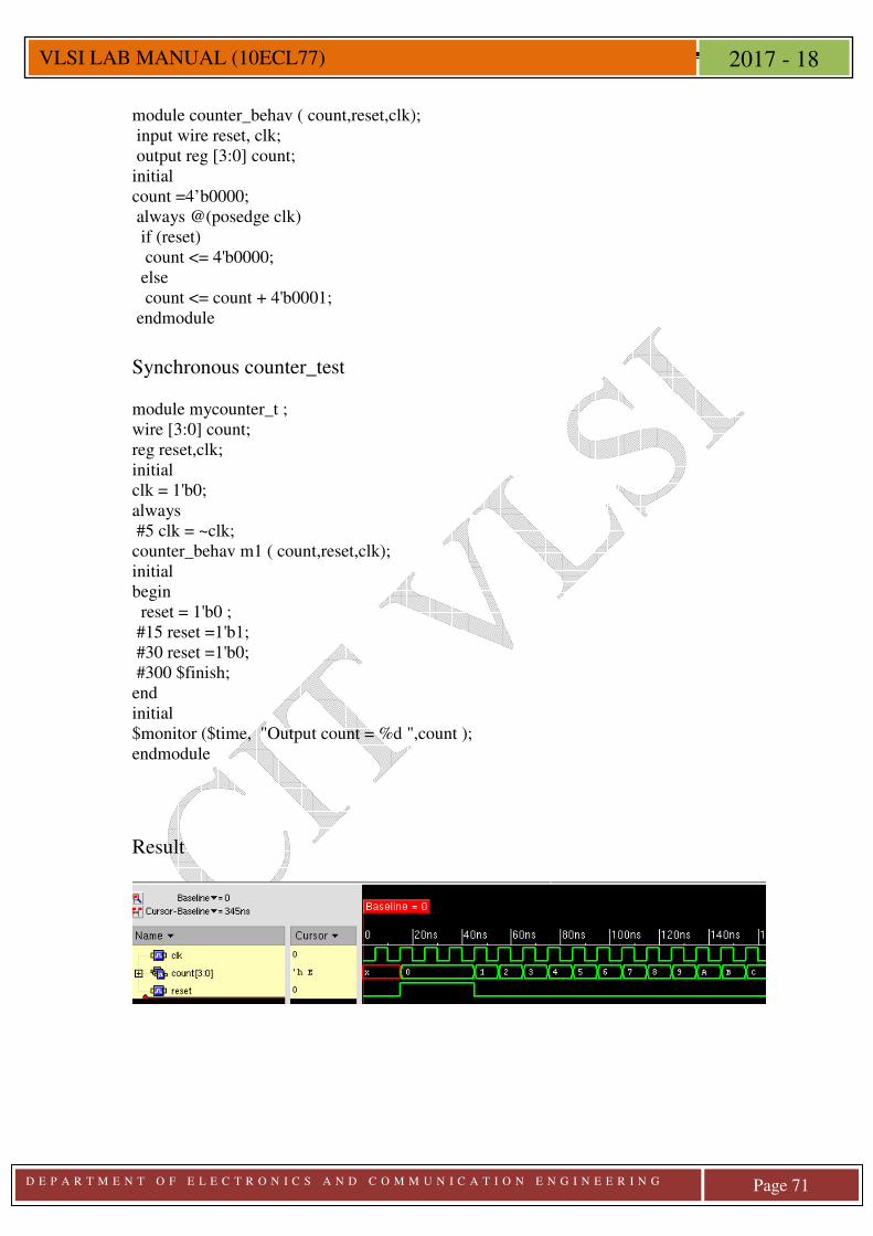
Result
D E P A R T M E N T O F E L E C T R O N I C S A N D C O M M U N I C A T I O N E N G I N E E R I N G
Page 72
VLSI LAB MANUAL (10ECL77) 2017 - 18
LAB 8: SUCCESSIVE APPROXIMATION REGISTER Aim: To compile and to simulate the Verilog code for the successive approximation register. Design Files: I Main Design Module: sar.v module sar (digitalout,done,comp,start,reset,clk); output [3:0] digitalout; output done; input clk, start, reset, comp; reg [3:0]ring_count; reg [3:0]digital; wire D4,set0,set1,set2,set3; assign D4 = ring_count[0]; assign done = !D4; always @(posedge clk or negedge reset) begin if (~reset) ring_count <= 4'b1000; else begin if (start) ring_count <= 4'b1000; else ring_count <= (ring_count>>1); end end assign set3 = ring_count[3]; assign set2 = ring_count[2]; assign set1 = ring_count[1]; assign set0 = ring_count[0]; always @(posedge clk or negedge reset) begin if(~reset) digital[3] <= 1'b1; else if(start) digital[3] <= 1'b1; else if(set3) digital[3] <= comp; end always @(posedge clk or negedge reset) begin if(~reset) digital[2] <= 1'b1; else if(start)
D E P A R T M E N T O F E L E C T R O N I C S A N D C O M M U N I C A T I O N E N G I N E E R I N G
Page 73
VLSI LAB MANUAL (10ECL77) 2017 - 18
digital[2] <= 1'b1; else if(set2) digital[2] <= comp; end always @(posedge clk or negedge reset) begin if(~reset) digital[1] <= 1'b1; else if(start) digital[1] <= 1'b1; else if(set1) digital[1] <= comp; end always @(posedge clk or negedge reset) begin if(~reset) digital[0] <= 1'b1; else if(start) digital[0] <= 1'b1; else if(set0) digital[0] <= comp; end assign digitalout = (digital) | (ring_count); endmodule II Sub Design Module: dac.v module dac (comp,sar_out,vref_d,vin_d,clk,start); output comp; input clk,start; input [3:0]sar_out; input [63:0]vref_d; input [63:0]vin_d; reg comp; real v_dac,vref,vin; always @ (vin_d or start) begin vref = $bitstoreal(vref_d); vin = $bitstoreal(vin_d); end always @* begin if(start) comp = 1'b0; else begin v_dac = (vref/15)*(sar_out); if (vin<v_dac)
D E P A R T M E N T O F E L E C T R O N I C S A N D C O M M U N I C A T I O N E N G I N E E R I N G
Page 74
VLSI LAB MANUAL (10ECL77) 2017 - 18
comp = 1'b0; else comp = 1'b1; end end endmodule III Test Bench Module: sar_tb.v module sar_tb; reg clk,reset,start; reg [63:0] vref_d,vin_d; wire done, comp; wire [3:0] digitalout; real vref_real = 7.5; sar s1 (digitalout,done,comp,start,reset,clk); dac d1 (comp,digitalout,vref_d,vin_d,clk,start); initial begin clk = 1'b1; start = 1'b1; #4000 $finish; end always #10 clk = ~clk; initial begin #1;reset = 1'b1; #10; reset = 1'b0; #1; reset = 1'b1; end initial begin #10 ; stimulus (0.0,0.5,vref_real,8'd5); end task stimulus (input analog, input step, input reference, input [7:0]delay); real analog,step; real reference; begin while(analog <= reference) begin repeat(delay) @(posedge clk); start <= 1'b0; vref_d = $realtobits (reference); vin_d = $realtobits (analog); @(posedge done) analog = analog + step; @(posedge clk); start <= 1'b1;
D E P A R T M E N T O F E L E C T R O N I C S A N D C O M M U N I C A T I O N E N G I N E E R I N G
Page 75
VLSI LAB MANUAL (10ECL77) 2017 - 18
end end endtask endmodule
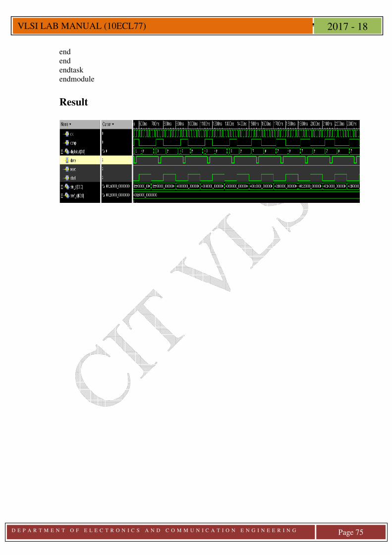
Result
D E P A R T M E N T O F E L E C T R O N I C S A N D C O M M U N I C A T I O N E N G I N E E R I N G
Page 76
VLSI LAB MANUAL (10ECL77) 2017 - 18
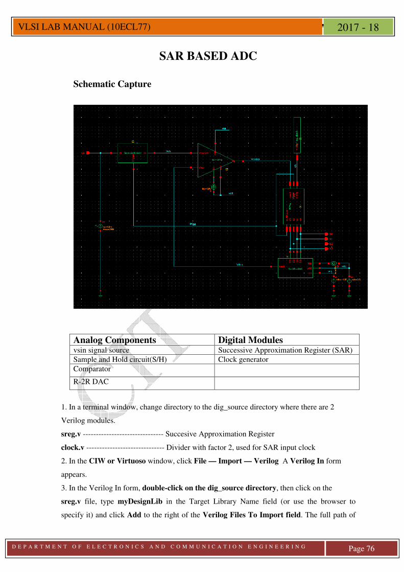
SAR BASED ADC
Schematic Capture
Analog Components Digital Modules vsin signal source Successive Approximation Register (SAR) Sample and Hold circuit(S/H) Clock generator Comparator R-2R DAC
1. In a terminal window, change directory to the dig_source directory where there are 2
Verilog modules.
sreg.v ------------------------------- Succesive Approximation Register
clock.v ------------------------------ Divider with factor 2, used for SAR input clock
2. In the CIW or Virtuoso window, click File — Import — Verilog A Verilog In form
appears.
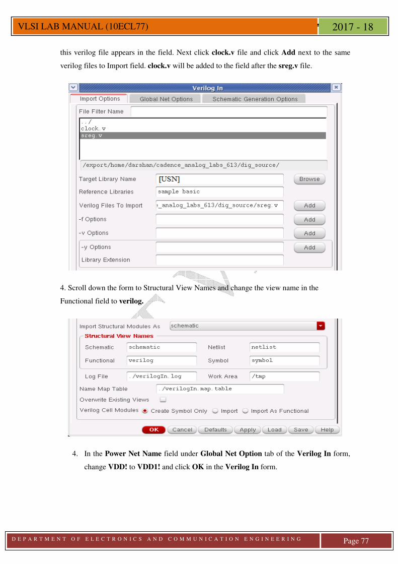
3. In the Verilog In form, double-click on the dig_source directory, then click on the
sreg.v file, type myDesignLib in the Target Library Name field (or use the browser to
specify it) and click Add to the right of the Verilog Files To Import field. The full path of
D E P A R T M E N T O F E L E C T R O N I C S A N D C O M M U N I C A T I O N E N G I N E E R I N G
Page 77
VLSI LAB MANUAL (10ECL77) 2017 - 18
this verilog file appears in the field. Next click clock.v file and click Add next to the same
verilog files to Import field. clock.v will be added to the field after the sreg.v file.
4. Scroll down the form to Structural View Names and change the view name in the
Functional field to verilog.
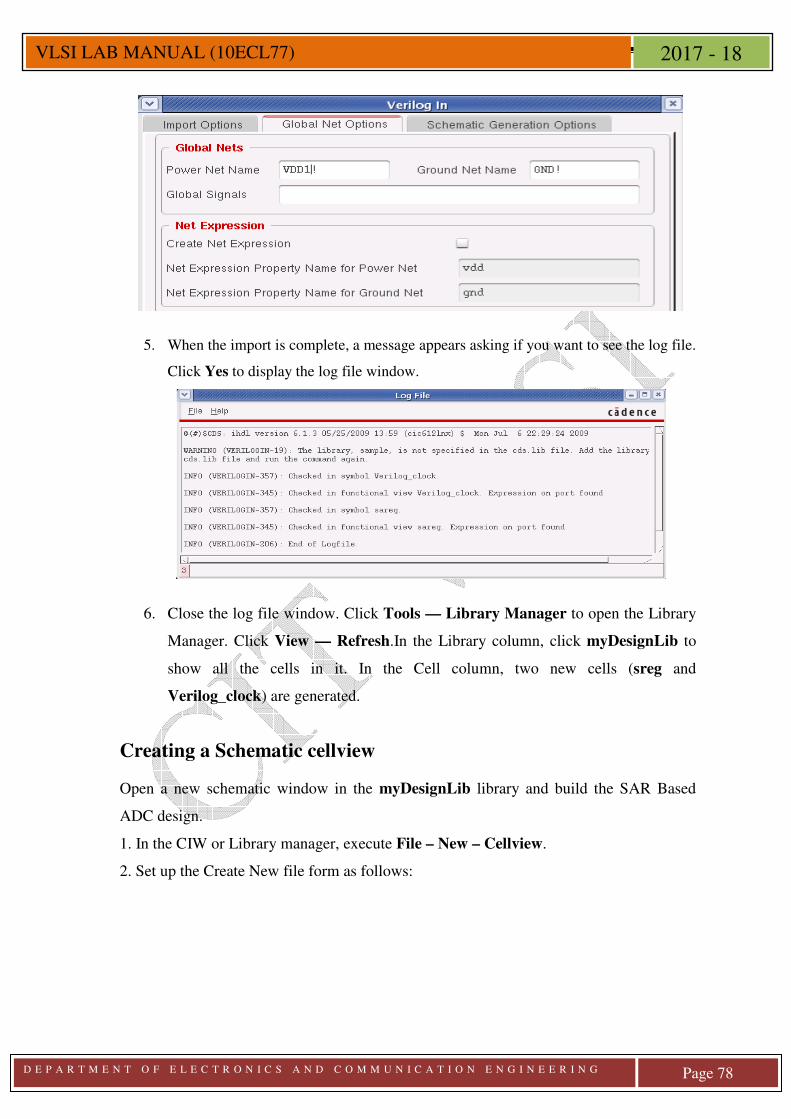
4. In the Power Net Name field under Global Net Option tab of the Verilog In form,
change VDD! to VDD1! and click OK in the Verilog In form.
D E P A R T M E N T O F E L E C T R O N I C S A N D C O M M U N I C A T I O N E N G I N E E R I N G
Page 78
VLSI LAB MANUAL (10ECL77) 2017 - 18
5. When the import is complete, a message appears asking if you want to see the log file.
Click Yes to display the log file window.
6. Close the log file window. Click Tools — Library Manager to open the Library
Manager. Click View — Refresh.In the Library column, click myDesignLib to
show all the cells in it. In the Cell column, two new cells (sreg and
Verilog_clock) are generated.
Creating a Schematic cellview
Open a new schematic window in the myDesignLib library and build the SAR Based
ADC design.
1. In the CIW or Library manager, execute File – New – Cellview.
2. Set up the Create New file form as follows:
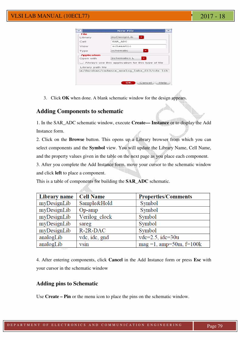
D E P A R T M E N T O F E L E C T R O N I C S A N D C O M M U N I C A T I O N E N G I N E E R I N G
Page 79
VLSI LAB MANUAL (10ECL77) 2017 - 18
3. Click OK when done. A blank schematic window for the design appears.
Adding Components to schematic
1. In the SAR_ADC schematic window, execute Create— Instance or to display the Add
Instance form.
2. Click on the Browse button. This opens up a Library browser from which you can
select components and the Symbol view. You will update the Library Name, Cell Name,
and the property values given in the table on the next page as you place each component.
3. After you complete the Add Instance form, move your cursor to the schematic window
and click left to place a component.
This is a table of components for building the SAR_ADC schematic.
4. After entering components, click Cancel in the Add Instance form or press Esc with
your cursor in the schematic window
Adding pins to Schematic Use Create – Pin or the menu icon to place the pins on the schematic window.
D E P A R T M E N T O F E L E C T R O N I C S A N D C O M M U N I C A T I O N E N G I N E E R I N G
Page 80
VLSI LAB MANUAL (10ECL77) 2017 - 18
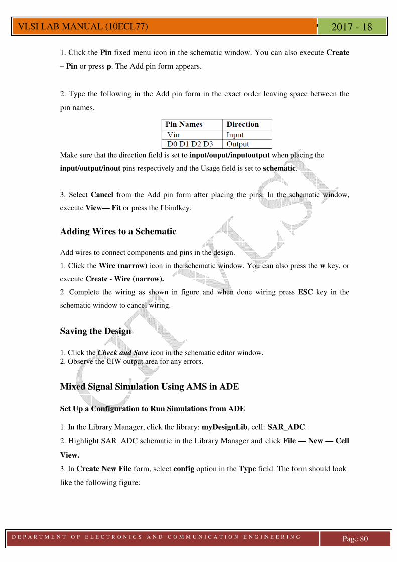
1. Click the Pin fixed menu icon in the schematic window. You can also execute Create
– Pin or press p. The Add pin form appears.
2. Type the following in the Add pin form in the exact order leaving space between the
pin names.
Make sure that the direction field is set to input/ouput/inputoutput when placing the
input/output/inout pins respectively and the Usage field is set to schematic.
3. Select Cancel from the Add pin form after placing the pins. In the schematic window,
execute View— Fit or press the f bindkey.
Adding Wires to a Schematic
Add wires to connect components and pins in the design.
1. Click the Wire (narrow) icon in the schematic window. You can also press the w key, or
execute Create - Wire (narrow).
2. Complete the wiring as shown in figure and when done wiring press ESC key in the
schematic window to cancel wiring.
Saving the Design 1. Click the Check and Save icon in the schematic editor window. 2. Observe the CIW output area for any errors.
Mixed Signal Simulation Using AMS in ADE
Set Up a Configuration to Run Simulations from ADE 1. In the Library Manager, click the library: myDesignLib, cell: SAR_ADC.
2. Highlight SAR_ADC schematic in the Library Manager and click File — New — Cell
View.
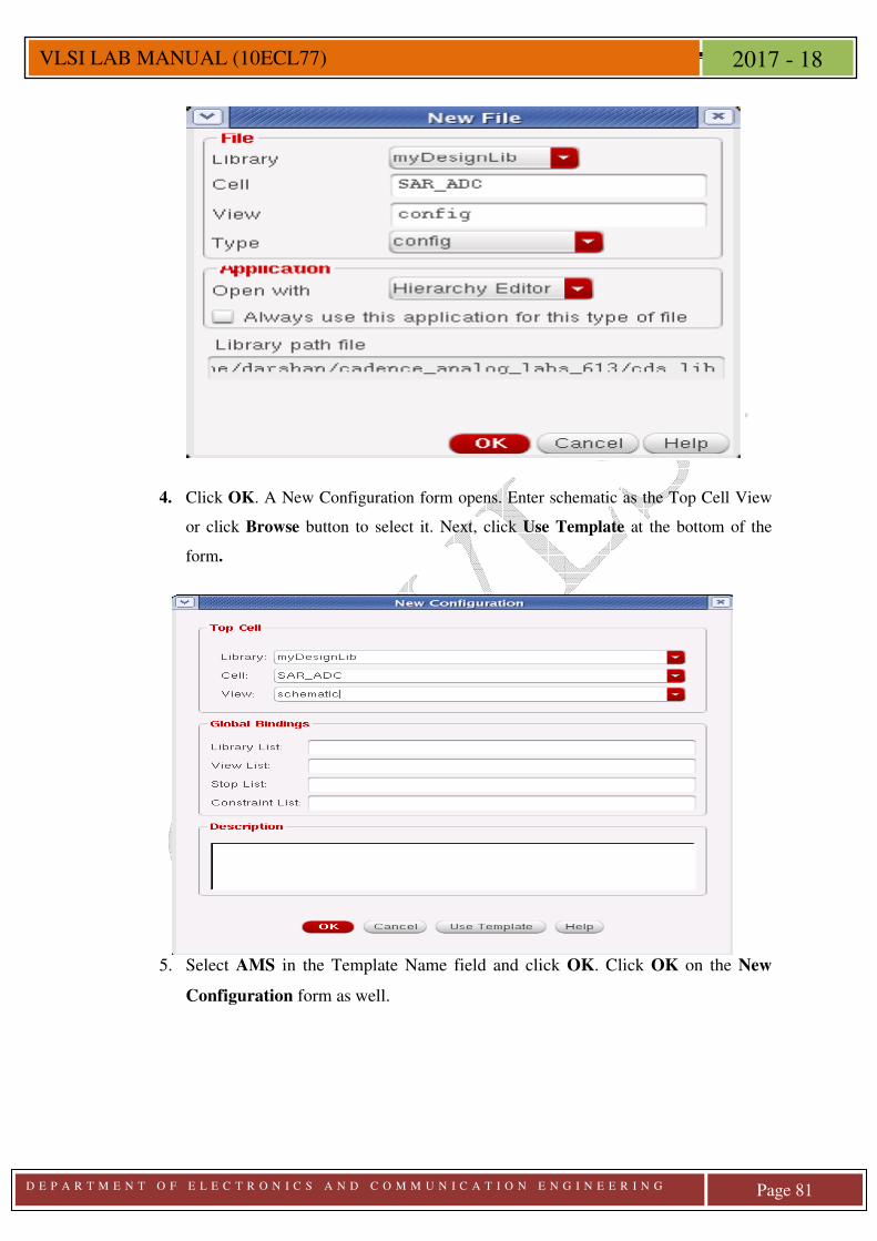
3. In Create New File form, select config option in the Type field. The form should look
like the following figure:
D E P A R T M E N T O F E L E C T R O N I C S A N D C O M M U N I C A T I O N E N G I N E E R I N G
Page 81
VLSI LAB MANUAL (10ECL77) 2017 - 18
4. Click OK. A New Configuration form opens. Enter schematic as the Top Cell View
or click Browse button to select it. Next, click Use Template at the bottom of the
form.
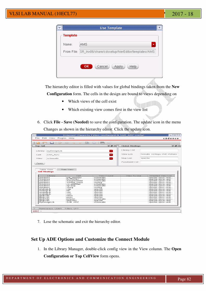
5. Select AMS in the Template Name field and click OK. Click OK on the New
Configuration form as well.
D E P A R T M E N T O F E L E C T R O N I C S A N D C O M M U N I C A T I O N E N G I N E E R I N G
Page 82
VLSI LAB MANUAL (10ECL77) 2017 - 18
The hierarchy editor is filled with values for global bindings taken from the New
Configuration form. The cells in the design are bound to views depending on
• Which views of the cell exist
• Which existing view comes first in the view list
6. Click File - Save (Needed) to save the configuration. The update icon in the menu
Changes as shown in the hierarchy editor. Click the update icon.
7. Lose the schematic and exit the hierarchy editor.
Set Up ADE Options and Customize the Connect Module
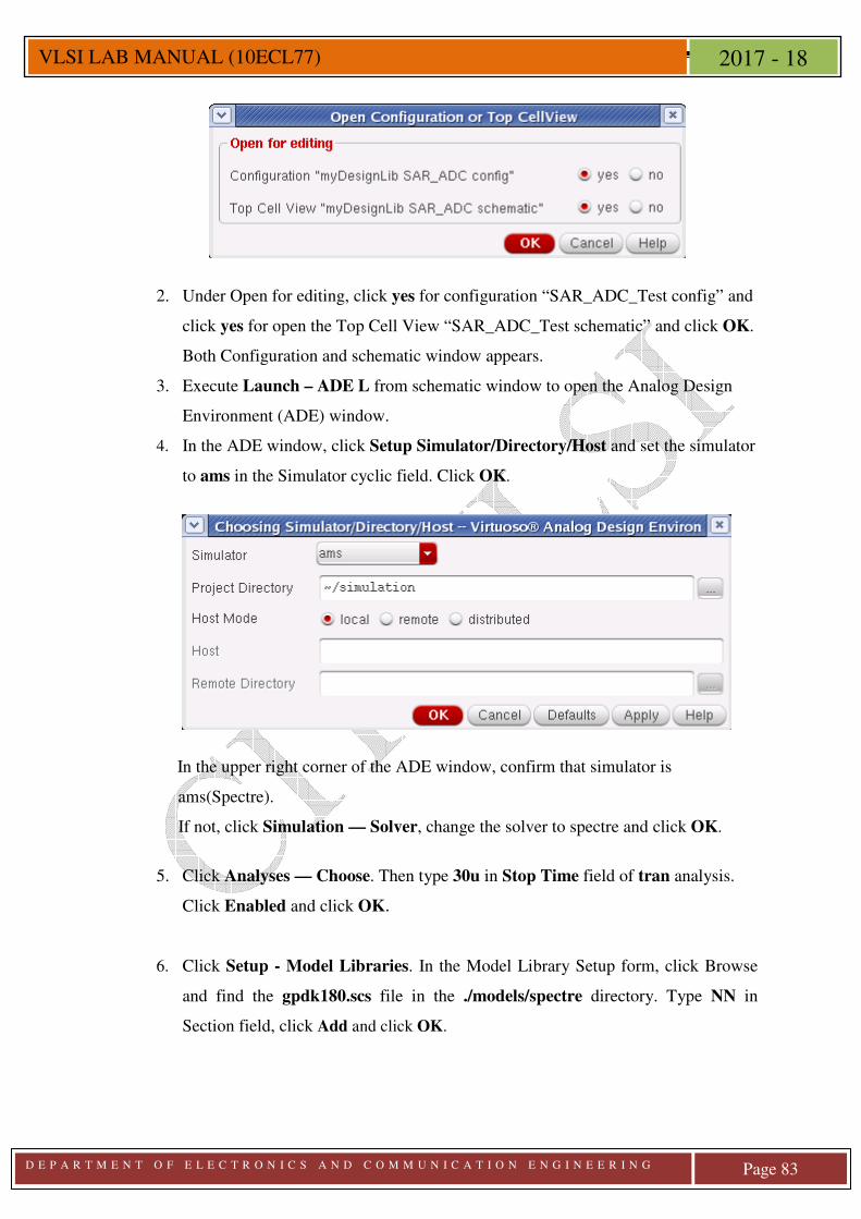
1. In the Library Manager, double-click config view in the View column. The Open
Configuration or Top CellView form opens.
D E P A R T M E N T O F E L E C T R O N I C S A N D C O M M U N I C A T I O N E N G I N E E R I N G
Page 83
VLSI LAB MANUAL (10ECL77) 2017 - 18
2. Under Open for editing, click yes for configuration “SAR_ADC_Test config” and
click yes for open the Top Cell View “SAR_ADC_Test schematic” and click OK.
Both Configuration and schematic window appears.
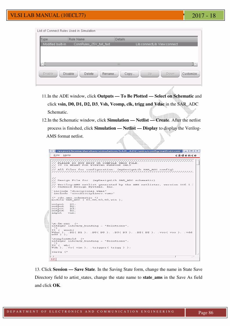
3. Execute Launch – ADE L from schematic window to open the Analog Design
Environment (ADE) window.
4. In the ADE window, click Setup Simulator/Directory/Host and set the simulator
to ams in the Simulator cyclic field. Click OK.
In the upper right corner of the ADE window, confirm that simulator is
ams(Spectre).
If not, click Simulation — Solver, change the solver to spectre and click OK.
5. Click Analyses — Choose. Then type 30u in Stop Time field of tran analysis.
Click Enabled and click OK.
6. Click Setup - Model Libraries. In the Model Library Setup form, click Browse
and find the gpdk180.scs file in the ./models/spectre directory. Type NN in
Section field, click Add and click OK.
D E P A R T M E N T O F E L E C T R O N I C S A N D C O M M U N I C A T I O N E N G I N E E R I N G
Page 84
VLSI LAB MANUAL (10ECL77) 2017 - 18
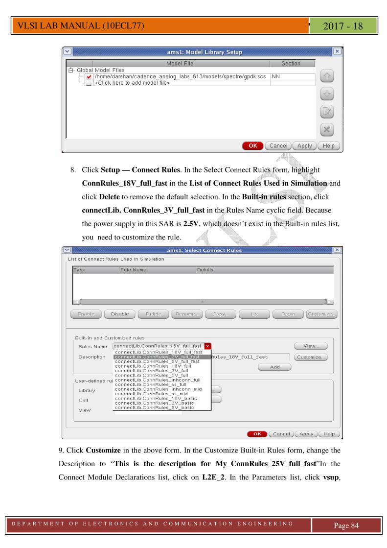
8. Click Setup — Connect Rules. In the Select Connect Rules form, highlight
ConnRules_18V_full_fast in the List of Connect Rules Used in Simulation and
click Delete to remove the default selection. In the Built-in rules section, click
connectLib. ConnRules_3V_full_fast in the Rules Name cyclic field. Because
the power supply in this SAR is 2.5V, which doesn’t exist in the Built-in rules list,
you need to customize the rule.
9. Click Customize in the above form. In the Customize Built-in Rules form, change the
Description to “This is the description for My_ConnRules_25V_full_fast”In the
Connect Module Declarations list, click on L2E_2. In the Parameters list, click vsup,
D E P A R T M E N T O F E L E C T R O N I C S A N D C O M M U N I C A T I O N E N G I N E E R I N G
Page 85
VLSI LAB MANUAL (10ECL77) 2017 - 18
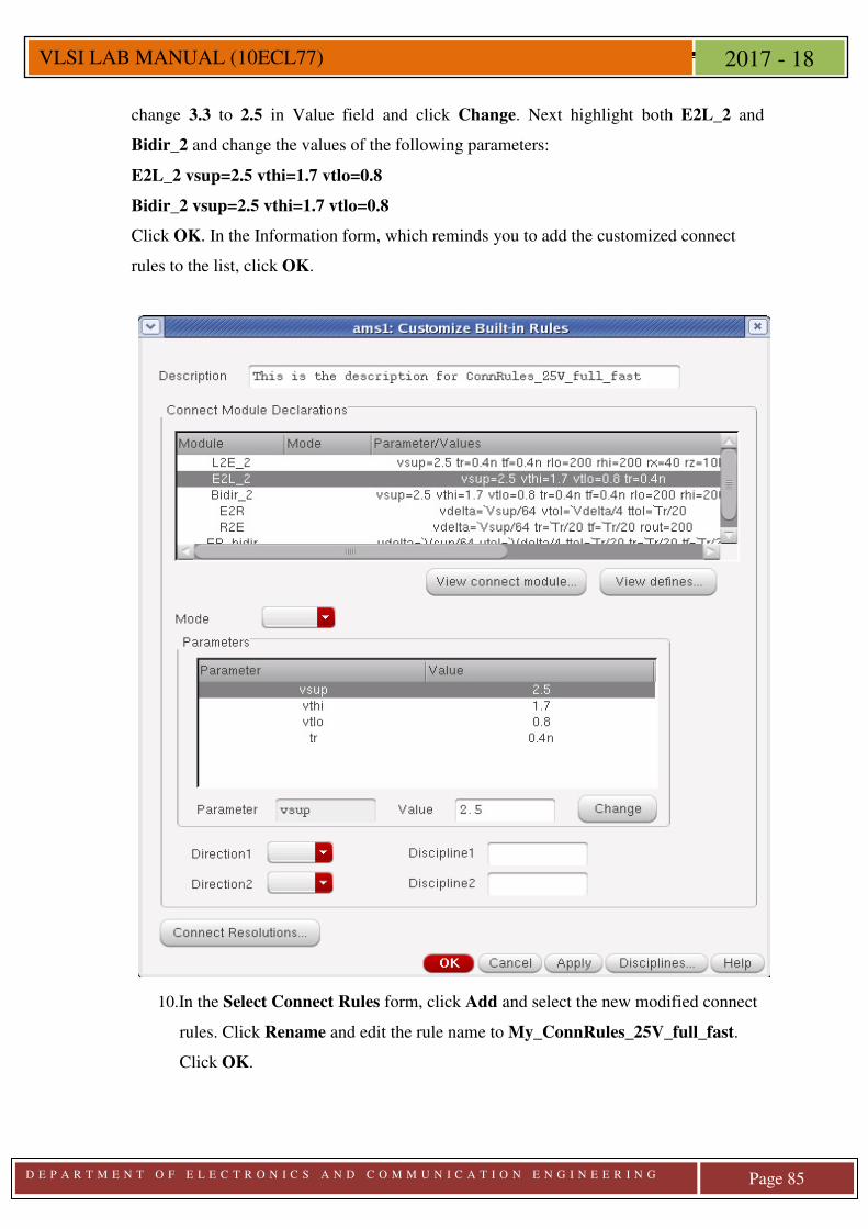
change 3.3 to 2.5 in Value field and click Change. Next highlight both E2L_2 and
Bidir_2 and change the values of the following parameters:
E2L_2 vsup=2.5 vthi=1.7 vtlo=0.8
Bidir_2 vsup=2.5 vthi=1.7 vtlo=0.8
Click OK. In the Information form, which reminds you to add the customized connect
rules to the list, click OK.
10.In the Select Connect Rules form, click Add and select the new modified connect
rules. Click Rename and edit the rule name to My_ConnRules_25V_full_fast.
Click OK.
D E P A R T M E N T O F E L E C T R O N I C S A N D C O M M U N I C A T I O N E N G I N E E R I N G
Page 86
VLSI LAB MANUAL (10ECL77) 2017 - 18
11.In the ADE window, click Outputs — To Be Plotted — Select on Schematic and
click vsin, D0, D1, D2, D3, Vsh, Vcomp, clk, trigg and Vdac in the SAR_ADC
Schematic.
12.In the Schematic window, click Simulation — Netlist — Create. After the netlist
process is finished, click Simulation — Netlist — Display to display the Verilog-
AMS format netlist.
13. Click Session — Save State. In the Saving State form, change the name in State Save
Directory field to artist_states, change the state name to state_ams in the Save As field
and click OK.
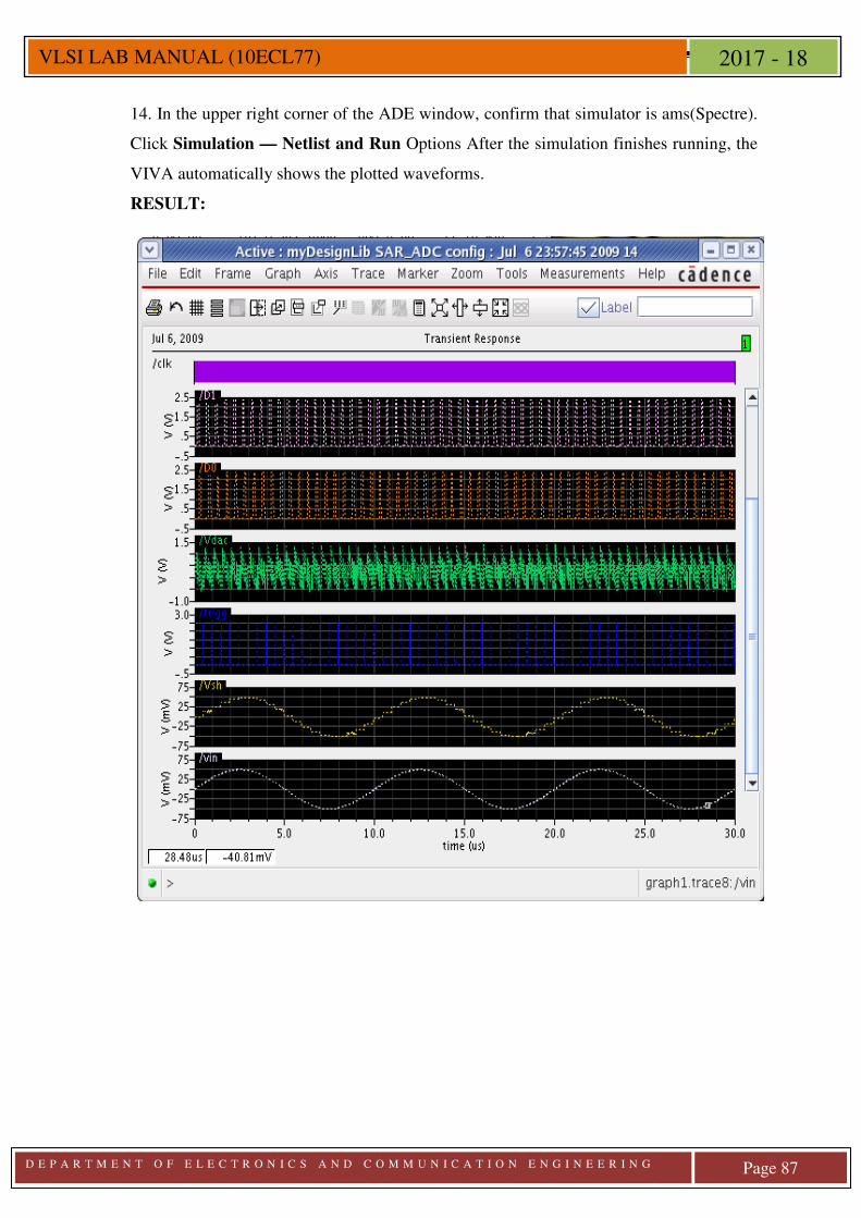
D E P A R T M E N T O F E L E C T R O N I C S A N D C O M M U N I C A T I O N E N G I N E E R I N G
Page 87
VLSI LAB MANUAL (10ECL77) 2017 - 18
14. In the upper right corner of the ADE window, confirm that simulator is ams(Spectre).
Click Simulation — Netlist and Run Options After the simulation finishes running, the
VIVA automatically shows the plotted waveforms.
RESULT:
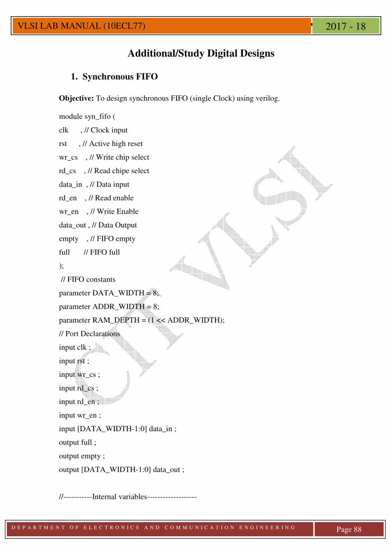
D E P A R T M E N T O F E L E C T R O N I C S A N D C O M M U N I C A T I O N E N G I N E E R I N G
Page 88
VLSI LAB MANUAL (10ECL77) 2017 - 18
Additional/Study Digital Designs
1. Synchronous FIFO
Objective: To design synchronous FIFO (single Clock) using verilog. module syn_fifo (
clk , // Clock input
rst , // Active high reset
wr_cs , // Write chip select
rd_cs , // Read chipe select
data_in , // Data input
rd_en , // Read enable
wr_en , // Write Enable
data_out , // Data Output
empty , // FIFO empty
full // FIFO full
);
// FIFO constants
parameter DATA_WIDTH = 8;
parameter ADDR_WIDTH = 8;
parameter RAM_DEPTH = (1 << ADDR_WIDTH);
// Port Declarations
input clk ;
input rst ;
input wr_cs ;
input rd_cs ;
input rd_en ;
input wr_en ;
input [DATA_WIDTH-1:0] data_in ;
output full ;
output empty ;
output [DATA_WIDTH-1:0] data_out ;
//-----------Internal variables-------------------
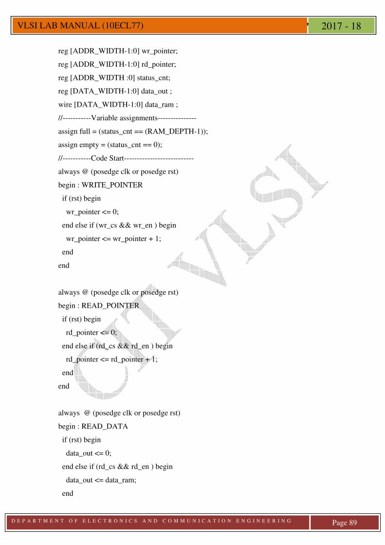
D E P A R T M E N T O F E L E C T R O N I C S A N D C O M M U N I C A T I O N E N G I N E E R I N G
Page 89
VLSI LAB MANUAL (10ECL77) 2017 - 18
reg [ADDR_WIDTH-1:0] wr_pointer;
reg [ADDR_WIDTH-1:0] rd_pointer;
reg [ADDR_WIDTH :0] status_cnt;
reg [DATA_WIDTH-1:0] data_out ;
wire [DATA_WIDTH-1:0] data_ram ;
//-----------Variable assignments---------------
assign full = (status_cnt == (RAM_DEPTH-1));
assign empty = (status_cnt == 0);
//-----------Code Start---------------------------
always @ (posedge clk or posedge rst)
begin : WRITE_POINTER
if (rst) begin
wr_pointer <= 0;
end else if (wr_cs && wr_en ) begin
wr_pointer <= wr_pointer + 1;
end
end
always @ (posedge clk or posedge rst)
begin : READ_POINTER
if (rst) begin
rd_pointer <= 0;
end else if (rd_cs && rd_en ) begin
rd_pointer <= rd_pointer + 1;
end
end
always @ (posedge clk or posedge rst)
begin : READ_DATA
if (rst) begin
data_out <= 0;
end else if (rd_cs && rd_en ) begin
data_out <= data_ram;
end
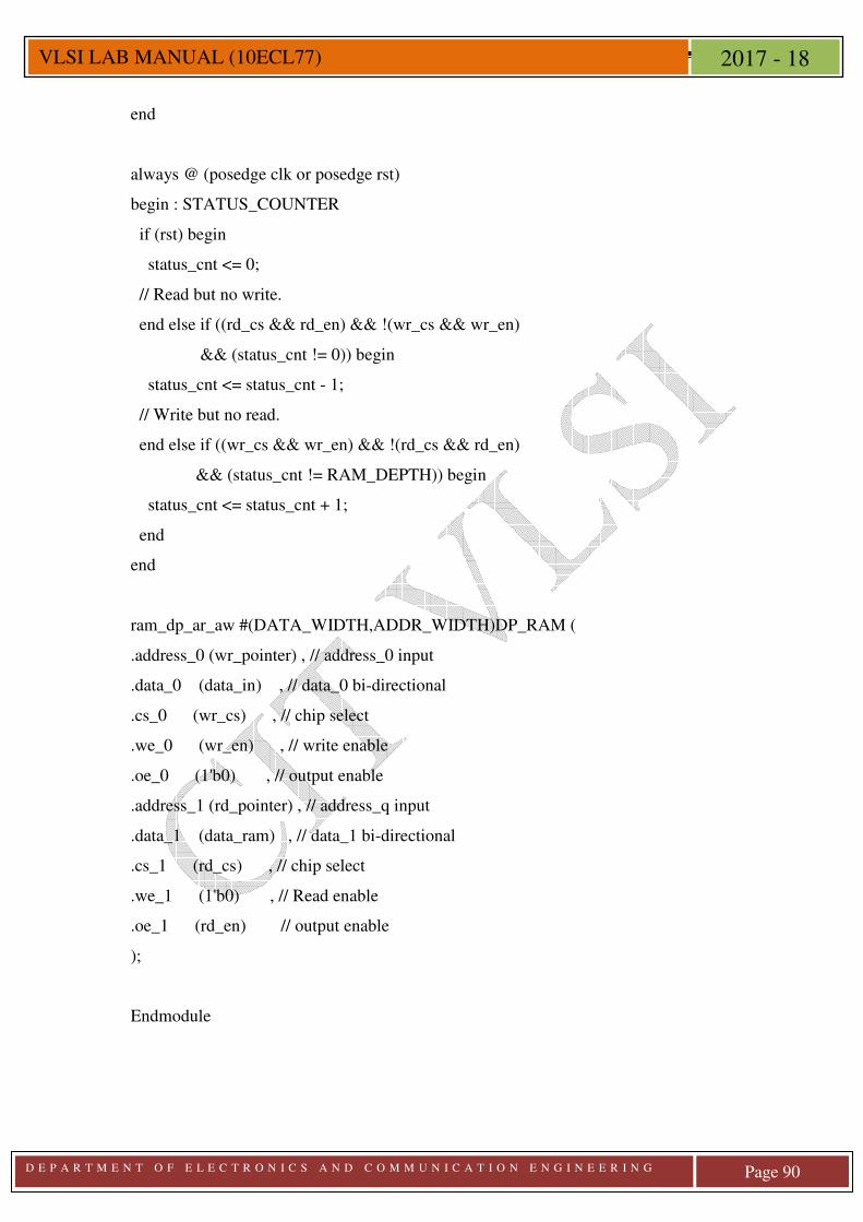
D E P A R T M E N T O F E L E C T R O N I C S A N D C O M M U N I C A T I O N E N G I N E E R I N G
Page 90
VLSI LAB MANUAL (10ECL77) 2017 - 18
end
always @ (posedge clk or posedge rst)
begin : STATUS_COUNTER
if (rst) begin
status_cnt <= 0;
// Read but no write.
end else if ((rd_cs && rd_en) && !(wr_cs && wr_en)
&& (status_cnt != 0)) begin
status_cnt <= status_cnt - 1;
// Write but no read.
end else if ((wr_cs && wr_en) && !(rd_cs && rd_en)
&& (status_cnt != RAM_DEPTH)) begin
status_cnt <= status_cnt + 1;
end
end
ram_dp_ar_aw #(DATA_WIDTH,ADDR_WIDTH)DP_RAM (
.address_0 (wr_pointer) , // address_0 input
.data_0 (data_in) , // data_0 bi-directional
.cs_0 (wr_cs) , // chip select
.we_0 (wr_en) , // write enable
.oe_0 (1'b0) , // output enable
.address_1 (rd_pointer) , // address_q input
.data_1 (data_ram) , // data_1 bi-directional
.cs_1 (rd_cs) , // chip select
.we_1 (1'b0) , // Read enable
.oe_1 (rd_en) // output enable
);
Endmodule
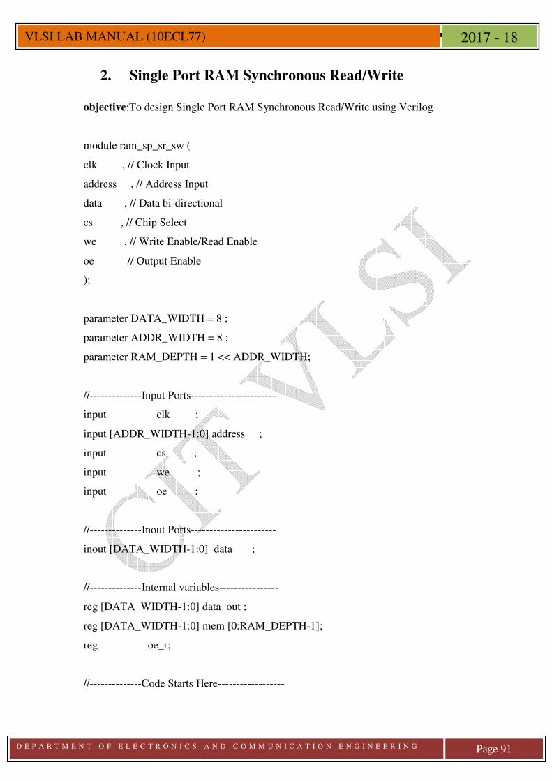
D E P A R T M E N T O F E L E C T R O N I C S A N D C O M M U N I C A T I O N E N G I N E E R I N G
Page 91
VLSI LAB MANUAL (10ECL77) 2017 - 18
2. Single Port RAM Synchronous Read/Write
objective:To design Single Port RAM Synchronous Read/Write using Verilog
module ram_sp_sr_sw (
clk , // Clock Input
address , // Address Input
data , // Data bi-directional
cs , // Chip Select
we , // Write Enable/Read Enable
oe // Output Enable
);
parameter DATA_WIDTH = 8 ;
parameter ADDR_WIDTH = 8 ;
parameter RAM_DEPTH = 1 << ADDR_WIDTH;
//--------------Input Ports-----------------------
input clk ;
input [ADDR_WIDTH-1:0] address ;
input cs ;
input we ;
input oe ;
//--------------Inout Ports-----------------------
inout [DATA_WIDTH-1:0] data ;
//--------------Internal variables----------------
reg [DATA_WIDTH-1:0] data_out ;
reg [DATA_WIDTH-1:0] mem [0:RAM_DEPTH-1];
reg oe_r;
//--------------Code Starts Here------------------
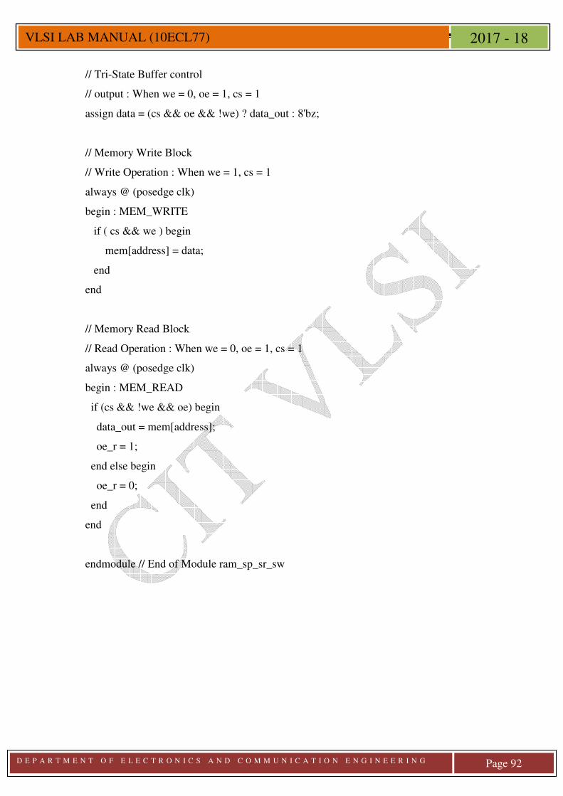
D E P A R T M E N T O F E L E C T R O N I C S A N D C O M M U N I C A T I O N E N G I N E E R I N G
Page 92
VLSI LAB MANUAL (10ECL77) 2017 - 18
// Tri-State Buffer control
// output : When we = 0, oe = 1, cs = 1
assign data = (cs && oe && !we) ? data_out : 8'bz;
// Memory Write Block
// Write Operation : When we = 1, cs = 1
always @ (posedge clk)
begin : MEM_WRITE
if ( cs && we ) begin
mem[address] = data;
end
end
// Memory Read Block
// Read Operation : When we = 0, oe = 1, cs = 1
always @ (posedge clk)
begin : MEM_READ
if (cs && !we && oe) begin
data_out = mem[address];
oe_r = 1;
end else begin
oe_r = 0;
end
end
endmodule // End of Module ram_sp_sr_sw
D E P A R T M E N T O F E L E C T R O N I C S A N D C O M M U N I C A T I O N E N G I N E E R I N G
Page 93
VLSI LAB MANUAL (10ECL77) 2017 - 18
QUESTION BANK
1. a) Design an Inverter with given specifications, completing the design flow mentioned below.
i. Draw the schematic and verify DC analysis and Transient analysis. ii. Draw the Layout, verify DRC, check for LVS and extract RC.
b) Write Verilog code and test bench for verification, for Parallel / Serial Adder and observe the waveform.
2. a) Design an Inverter with given specifications, completing the design flow mentioned below.
i. Draw the schematic and verify DC analysis and Transient analysis. ii. Draw the Layout, verify DRC, check for LVS and extract RC.
b) Write Verilog code and test bench for verification, for 4-bit Synchronous / Asynchronous Counter and observe the waveform
3. a) Design a Common Source Amplifier with given specifications, completing the design flow mentioned below.
i. Draw the schematic and verify AC analysis, DC analysis and Transient analysis.
ii. Draw the Layout, verify DRC, check for LVS and extract RC. b) Write Verilog code, their test bench for verification and observe the waveform for RS Flip Flop
4. a) Design a Common Drain Amplifier with given specifications, completing the design flow mentioned below.
i. Draw the schematic and verify AC analysis, DC analysis and Transient analysis.
ii. Draw the Layout, verify DRC, check for LVS and extract RC. b) Write Verilog code and test bench for verification, for an NAND Gate and observe the waveform.
5. a) Design a Differential Amplifier with given specifications, completing the design flow mentioned below.
i. Draw the schematic and verify AC analysis, DC analysis and Transient analysis.
ii. Draw the Layout, verify DRC, check for LVS and extract RC. b) Write Verilog code and test bench for verification, for a transmission gate and observe the waveform.
6. a) Design an Operational Amplifier ( Diff amp + CS amp ) with given specifications, completing the design flow mentioned below.
i. Draw the schematic and verify AC analysis, DC analysis and Transient analysis.
ii. Draw the Layout, verify DRC, check for LVS and extract RC. b) Write Verilog code and test bench for verification and observe the waveform for D FF.
7. a) Design a 4-bit R-2R based DAC with given specifications, completing the design flow mentioned below.
i. Draw the schematic and verify the Transient analysis. ii. Draw the Layout, verify DRC, check for LVS and extract RC.
b) Write Verilog code and test bench for verification, for an inverter and observe the waveform
8. a) Design a Common Source Amplifier with given specifications, completing the design flow mentioned below.
D E P A R T M E N T O F E L E C T R O N I C S A N D C O M M U N I C A T I O N E N G I N E E R I N G
Page 94
VLSI LAB MANUAL (10ECL77) 2017 - 18
i. Draw the schematic and verify AC analysis, DC analysis and Transient analysis.
ii. Draw the Layout, verify DRC, check for LVS and extract RC. b) Write Verilog code, their test bench for verification and observe the waveform for OR gate.
9. a) Design a Common Drain Amplifier with given specifications, completing the design flow mentioned below.
i. Draw the schematic and verify AC analysis, DC analysis and Transient analysis.
ii. Draw the Layout, verify DRC, check for LVS and extract RC. b) Write Verilog code and test bench for verification, for a JK FF and observe the waveform.
10. a) Design a Differential Amplifier with given specifications, completing the design flow mentioned below.
i. Draw the schematic and verify AC analysis, DC analysis and Transient analysis.
ii. Draw the Layout, verify DRC, check for LVS and extract RC. b) Write Verilog code and test bench for verification, for a buffer and observe the waveform.
11. a) Design a Common Source Amplifier with given specifications, completing the design flow mentioned below.
i. Draw the schematic and verify AC analysis, DC analysis and Transient analysis.
ii. Draw the Layout, verify DRC, check for LVS and extract RC. b) Write Verilog code, their test bench for verification and observe the waveform for AND gate
12. a) Design a Common Drain Amplifier with given specifications, completing the design flow mentioned below.
i. Draw the schematic and verify AC analysis, DC analysis and Transient analysis.
ii. Draw the Layout, verify DRC, check for LVS and extract RC. b) Write Verilog code, their test bench for verification and observe the waveform for XOR gate.
13. a) Design an Inverter with given specifications, completing the design flow mentioned below.
i. Draw the schematic and verify DC analysis and Transient analysis. ii. Draw the Layout, verify DRC, check for LVS and extract RC.
b) Write Verilog code and test bench for verification, for SAR based ADC and observe the waveform.
14. a) Design an Inverter with given specifications, completing the design flow mentioned below.
i. Draw the schematic and verify DC analysis and Transient analysis. ii. Draw the Layout, verify DRC, check for LVS and extract RC.
b) Write Verilog code and test bench for verification, for an XNOR gate and observe the waveform.

D E P A R T M E N T O F E L E C T R O N I C S A N D C O M M U N I C A T I O N E N G I N E E R I N G
Page 95
VLSI LAB MANUAL (10ECL77) 2017 - 18
VIVA – VOCE MODEL QUESTIONS
1. What is CMOS technology?
2. Which is the technology used in VLSI lab?
3. Explain ASIC design flow?
4. Explain the operation of NMOS and PMOS MOSFETS.
5. Explain the regions of operations for both NMOS and PMOS.
6. Which are majority carriers in NMOS and PMOS?
7. Explain the operation of CMOS inverter.
8. What is the difference between CMOS and BIPOLAR technology?
9. What are advantages and disadvantages of CMOS technology?
10. Explain 5 regions of operation for an inverter.
11. What is transient, DC and AC analysis?
12. What is noise margin?
13. What is channel length modulation?
14. What is HOT electron effect?
15. What is routing?
16. What is floor plan?
17. What is placement?
18. What is DRC, LVS?
19. Explain the fabrication process of both NMOS and PMOS.
20. What is an amplifier?
21. Write the design of common source and common drain amplifier.
22. What is differential amplifier? Explain the design.
23. What are CMRR, SNR, and PSRR?
24. What is operational amplifier and explain the basic building block of an OP-AMP?
25. Explain the design procedure of an OP-AMP.
26. What is test bench?
27. What is the difference between simulation and synthesis?
28. What is a buffer?
29. Explain the CMOS circuits for basic gates.
30. What is the difference between stick diagram and layout?
31. Which is the layer used to connect the components?
32. What are the different styles of programming?

D E P A R T M E N T O F E L E C T R O N I C S A N D C O M M U N I C A T I O N E N G I N E E R I N G
Page 96
VLSI LAB MANUAL (10ECL77) 2017 - 18
33. What is user defined packages?
34. What is the function of task and display?
35. Explain the operation of transmission gates.
36. Explain D flip-flop with truth table?
37. Explain T flip-flop with truth table?
38. Explain JK flip-flop with truth table?
39. Explain SR flip-flop with truth table?
40. Explain MS flip-flop with truth table?
41. What are glitches?
42. What is pinch of region?
43. What is setup and hold time?
44. What is race around condition?
45. Explain latch up problem with circuit.
46. How to overcome from latch up problem?
47. What is the difference between serial adder and parallel adder?
48. Explain the circuits for half adder and full adder.
49. What is the difference between asynchronous and synchronous counter?
50. Design ripple counter?
51. Design a synchronous counter for given mod.
52. Write the layout for the basic gates and given expression.
53. Write the stick diagram for the basic gates and given expression.
54. Write the color code for n+ and p+ diffusion?
55. What is lambda based design rules?
56. What is metallization?
57. What are Vias and guard rings?
58. What is a function?
59. What are diffusion, oxidation, ion implantation and etching?
60. What is SOI?
D E P A R T M E N T O F E L E C T R O N I C S A N D C O M M U N I C A T I O N E N G I N E E R I N G
Page 97
VLSI LAB MANUAL (10ECL77) 2017 - 18
REFERENCES
[1] Design of analog CMOS integrated circuits, B Razavi, First Edition, Mcgraw Hill 2001
[2] Design, Layout, simulation, R.jacob Baker, Harry W Li, David E Boyci, CMOS
Circuit, PHI edition , 2005.
[3] CMOS Mixed Signal Circuit Design (Vol II of CMOS: Circuit design, Layout and simulation), R. Jacob. Baker, CMOS-IEEE press and wiley interscience 2002.
[4] CMOS analog circuit design, P E Allen and D R Holberg , Second Edition ,
oxford university press 2002.
[5] Fundamentals of logic design with VHDL, Stephen Brown & Zvonko vranesic, Tata McGraw-Hill, New Delhi, Second Edition, 2007.
[6] Verilog HDL: A guide to digital design and synthesis, Samir palnitkar, Second edition