Embed Size (px)
Citation preview
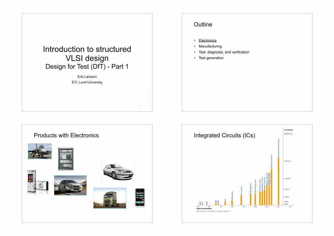
Introduction to structured VLSI design
Design for Test (DfT) - Part 1Erik Larsson
EIT, Lund University
Outline
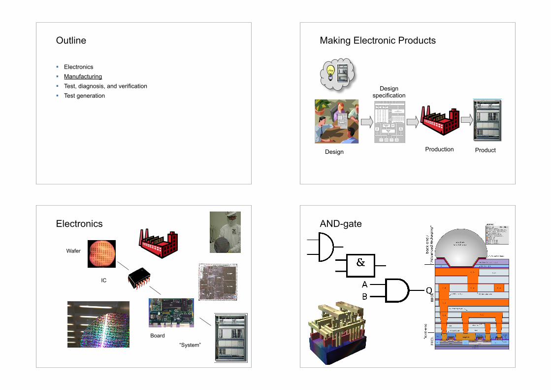
! Electronics! Manufacturing! Test, diagnosis, and verification! Test generation
Products with Electronics Integrated Circuits (ICs)
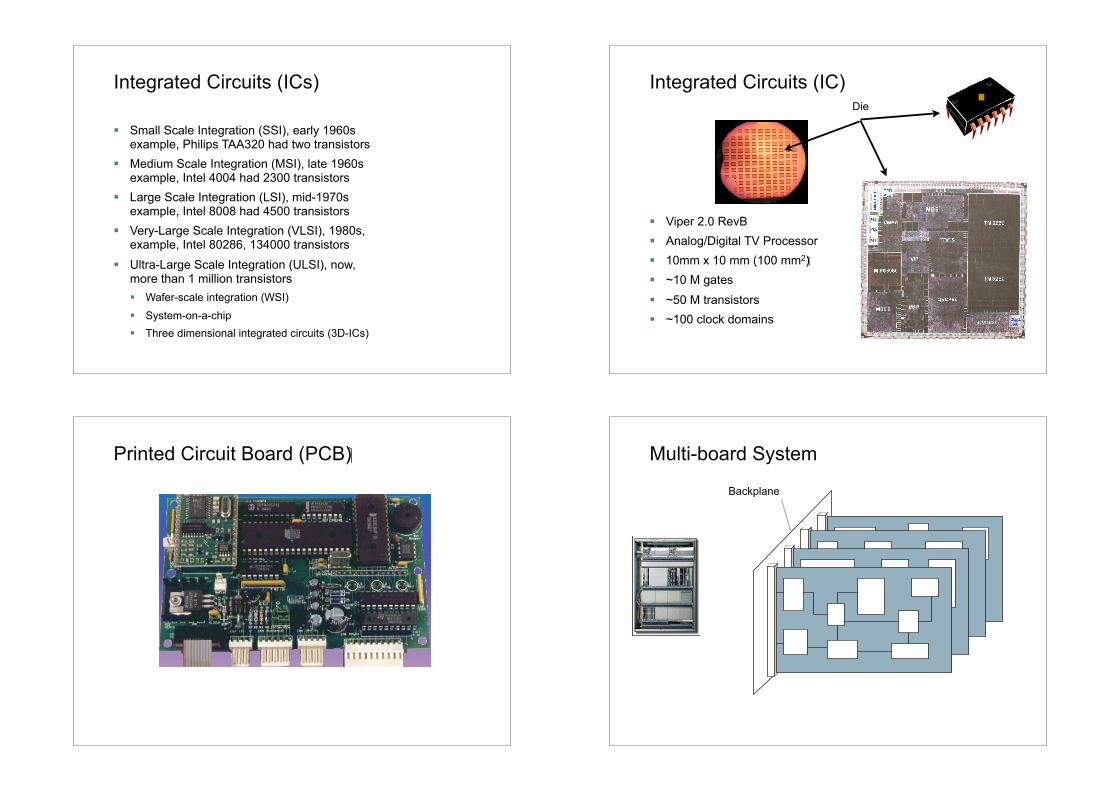
Integrated Circuits (ICs)
! Small Scale Integration (SSI), early 1960sexample, Philips TAA320 had two transistors
! Medium Scale Integration (MSI), late 1960sexample, Intel 4004 had 2300 transistors
! Large Scale Integration (LSI), mid-1970sexample, Intel 8008 had 4500 transistors
! Very-Large Scale Integration (VLSI), 1980s,example, Intel 80286, 134000 transistors
! Ultra-Large Scale Integration (ULSI), now,more than 1 million transistors! Wafer-scale integration (WSI)
! System-on-a-chip! Three dimensional integrated circuits (3D-ICs)
Integrated Circuits (IC)
! Viper 2.0 RevB! Analog/Digital TV Processor! 10mm x 10 mm (100 mm2)! ~10 M gates! ~50 M transistors! ~100 clock domains
Die
Printed Circuit Board (PCB) Multi-board System
Backplane
Outline
! Electronics! Manufacturing! Test, diagnosis, and verification! Test generation
Making Electronic Products
Production Product
Design specification
Design
Electronics
Wafer
IC
Board
“System”
AND-gate
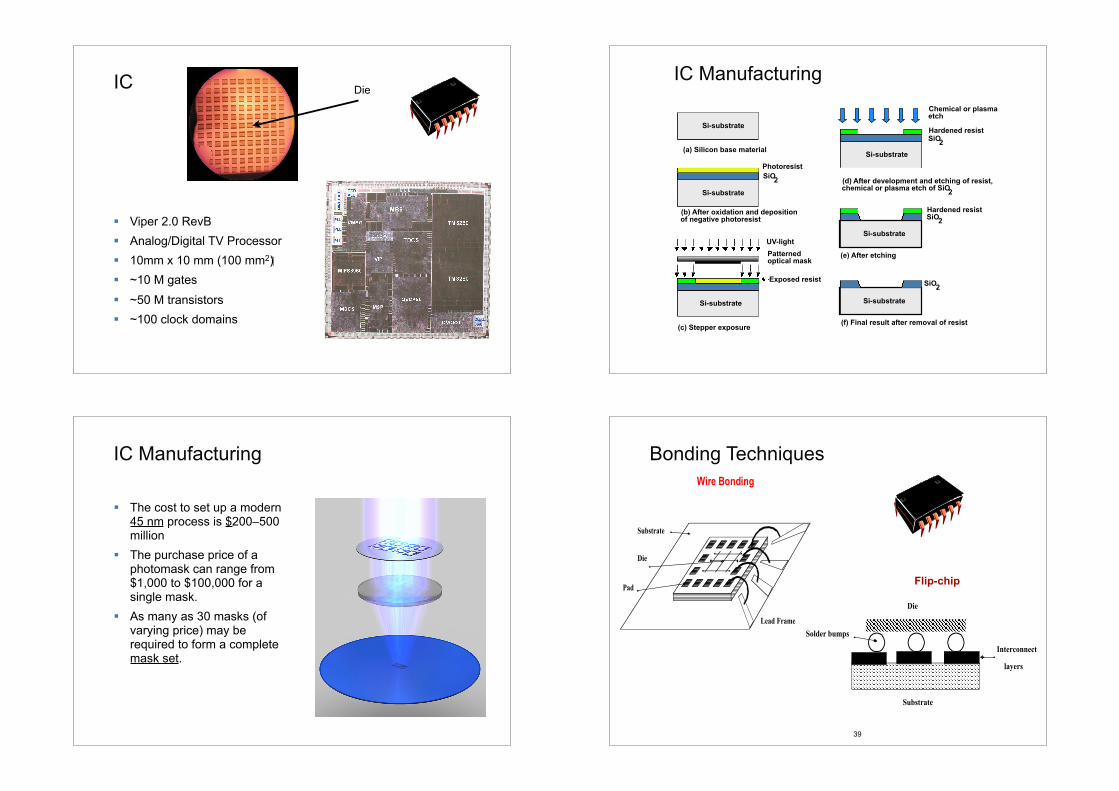
IC
! Viper 2.0 RevB! Analog/Digital TV Processor! 10mm x 10 mm (100 mm2)! ~10 M gates! ~50 M transistors! ~100 clock domains
DieIC Manufacturing
Si-substrate
Si-substrate Si-substrate
(a) Silicon base material
(b) After oxidation and depositionof negative photoresist
(c) Stepper exposure
PhotoresistSiO2
UV-lightPatternedoptical mask
Exposed resist
SiO2
Si-substrate
Si-substrate
Si-substrate
SiO2
SiO2
(d) After development and etching of resist,chemical or plasma etch of SiO2
(e) After etching
(f) Final result after removal of resist
Hardened resist
Hardened resist
Chemical or plasmaetch
IC Manufacturing
! The cost to set up a modern 45 nm process is $200–500 million
! The purchase price of a photomask can range from $1,000 to $100,000 for a single mask.
! As many as 30 masks (of varying price) may be required to form a complete mask set.
39
Bonding Techniques
Flip-chip
42
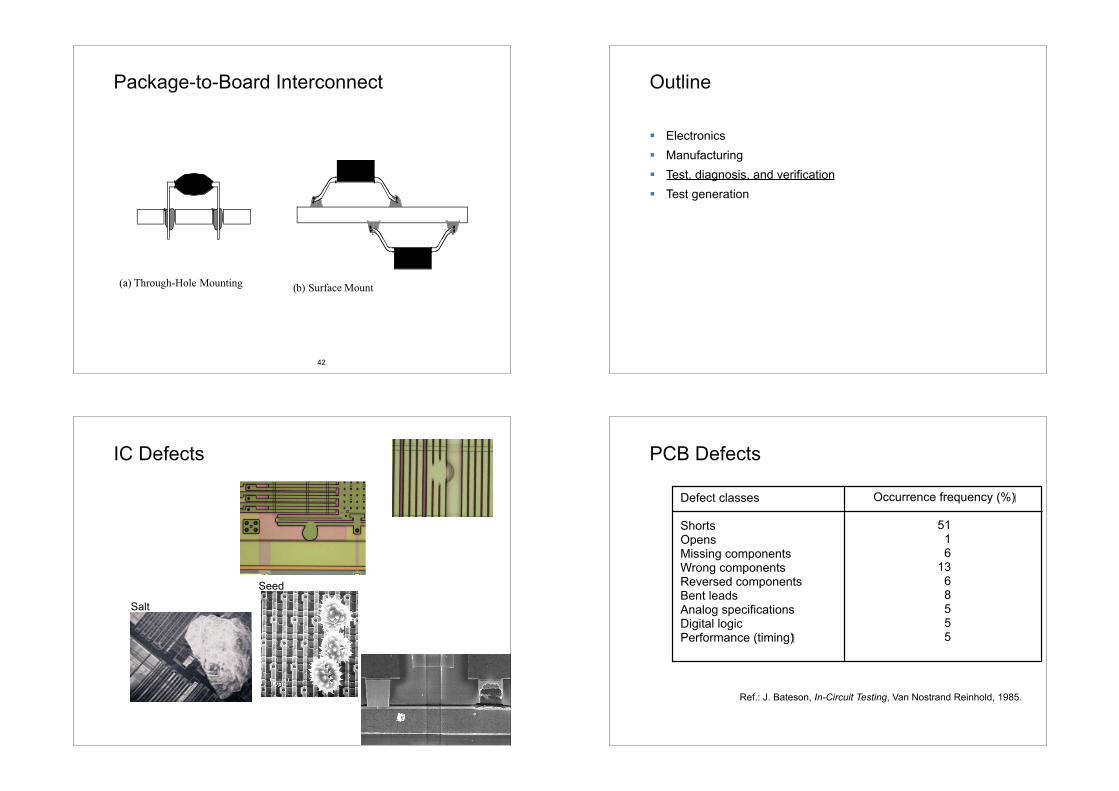
Package-to-Board Interconnect Outline
! Electronics! Manufacturing! Test, diagnosis, and verification! Test generation
IC Defects
Salt
Seed
PCB Defects
Ref.: J. Bateson, In-Circuit Testing, Van Nostrand Reinhold, 1985.
Defect classes
ShortsOpensMissing componentsWrong componentsReversed componentsBent leadsAnalog specificationsDigital logicPerformance (timing)
Occurrence frequency (%)
51 1 613 6 8 5 5 5
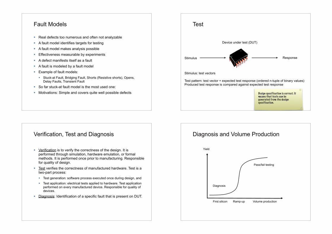
Fault Models
! Real defects too numerous and often not analyzable! A fault model identifies targets for testing! A fault model makes analysis possible! Effectiveness measurable by experiments ! A defect manifests itself as a fault! A fault is modeled by a fault model! Example of fault models:
! Stuck-at Fault, Bridging Fault, Shorts (Resistive shorts), Opens, Delay Faults, Transient Fault
! So far stuck-at fault model is the most used one: ! Motivations: Simple and covers quite well possible defects
Test
Device under test (DUT)
Stimulus
Stimulus: test vectors
Test pattern: test vector + expected test response (ordered n-tuple of binary values)Produced test response is compared against expected test response
Response
Design specification is correct. It means that tests can be generated from the design specification.
Verification, Test and Diagnosis
! Verification is to verify the correctness of the design. It is performed through simulation, hardware emulation, or formal methods. It is performed once prior to manufacturing. Responsible for quality of design.
! Test verifies the correctness of manufactured hardware. Test is a two-part process: ! Test generation: software process executed once during design, and ! Test application: electrical tests applied to hardware. Test application
performed on every manufactured device. Responsible for quality of devices.
! Diagnosis: Identification of a specific fault that is present on DUT.
Diagnosis and Volume Production
Yield
First silicon Ramp-up Volume production
Diagnosis
Pass/fail testing
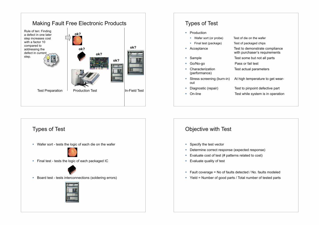
Making Fault Free Electronic Products
ok?
Test Preparation Production Test In-Field Test
ok?ok?
ok?
ok?
Rule of ten: Finding a defect in one later step increases cost with a factor 10 compared to addressing the defect in current step.
Types of Test! Production
! Wafer sort (or probe) Test of die on the wafer
! Final test (package) Test of packaged chips
! Acceptance Test to demonstrate compliance with purchaser’s requirements
! Sample Test some but not all parts ! Go/No-go Pass or fail test! Characterization Test actual parameters
(performance)! Stress screening (burn-in) At high temperature to get wear-
out! Diagnostic (repair) Test to pinpoint defective part! On-line Test while system is in operation
Types of Test
! Wafer sort - tests the logic of each die on the wafer
! Final test - tests the logic of each packaged IC
! Board test - tests interconnections (soldering errors)
Objective with Test
! Specify the test vector! Determine correct response (expected response)! Evaluate cost of test (# patterns related to cost)! Evaluate quality of test
! Fault coverage = No of faults detected / No. faults modeled! Yield = Number of good parts / Total number of tested parts
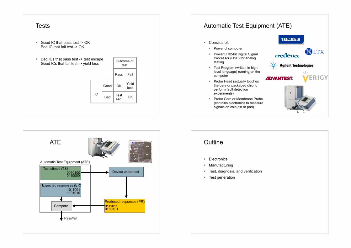
Tests
! Good IC that pass test -> OKBad IC that fail test -> OK
! Bad ICs that pass test -> test escapeGood ICs that fail test -> yield loss
Outcome of test
Outcome of test
Pass Fail
IC
Good OK Yield loss
ICBad Test
esc. OK
Automatic Test Equipment (ATE)
! Consists of:! Powerful computer
! Powerful 32-bit Digital Signal Processor (DSP) for analog testing
! Test Program (written in high-level language) running on the computer
! Probe Head (actually touches the bare or packaged chip to perform fault detection experiments)
! Probe Card or Membrane Probe(contains electronics to measure signals on chip pin or pad)
ATE
Device under test00101000110000
Test stimuli (TS)
Compare
Automatic Test Equipment (ATE)
Pass/fail
Expected responses (ER) 10110011101010
01110110100101
Produced responses (PR)
Outline
! Electronics! Manufacturing! Test, diagnosis, and verification! Test generation
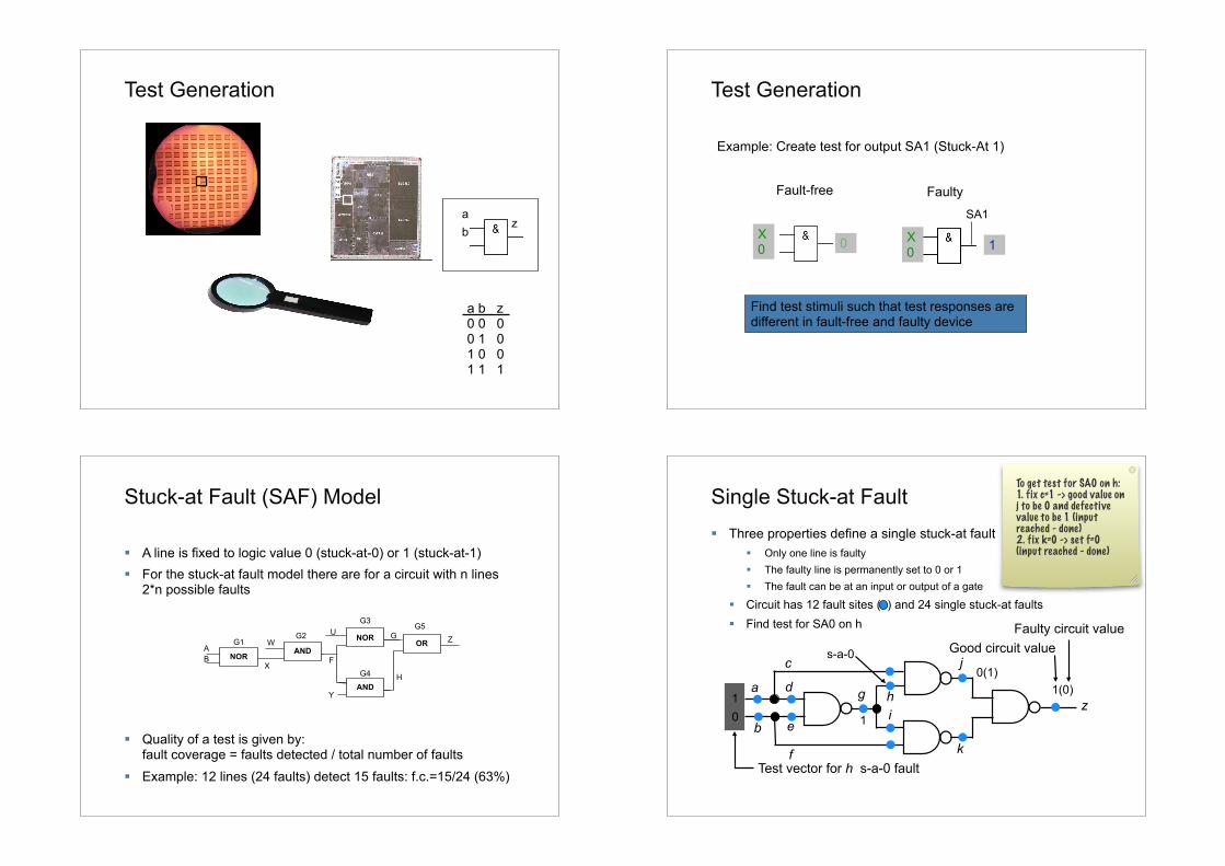
Test Generation
ab
z
a b z0 0 00 1 01 0 01 1 1
Test Generation
FaultySA1
Fault-free
X0
X0
0 1
Example: Create test for output SA1 (Stuck-At 1)
Find test stimuli such that test responses are different in fault-free and faulty device
Stuck-at Fault (SAF) Model
! A line is fixed to logic value 0 (stuck-at-0) or 1 (stuck-at-1)! For the stuck-at fault model there are for a circuit with n lines
2*n possible faults
! Quality of a test is given by: fault coverage = faults detected / total number of faults
! Example: 12 lines (24 faults) detect 15 faults: f.c.=15/24 (63%)
ORNOR
AZ
BAND
NOR
AND
UW
X
Y
F
H
GG1
G2
G3
G4
G5
Single Stuck-at Fault! Three properties define a single stuck-at fault
! Only one line is faulty! The faulty line is permanently set to 0 or 1! The fault can be at an input or output of a gate
! Circuit has 12 fault sites ( ) and 24 single stuck-at faults! Find test for SA0 on h
a
b
c
d
e
f
10
g h i 1
s-a-0j
k
z
0(1)1(0)
Test vector for h s-a-0 fault
Good circuit valueFaulty circuit value
To get test for SA0 on h: 1. fix c=1 -> good value on j to be 0 and defective value to be 1 (input reached - done)2. fix k=0 -> set f=0 (input reached - done)
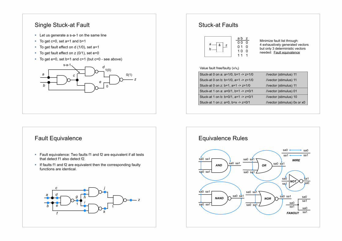
Single Stuck-at Fault! Let us generate a s-a-1 on the same line ! To get c=0, set a=1 and b=1! To get fault effect on d (1/0), set a=1! To get fault effect on z (0/1), set e=0! To get e=0, set b=1 and c=1 (but c=0 - see above)
a
b
c
d
e
s-a-1
z
1(0)0(1)
0
Stuck-at Faults
a b z0 0 00 1 01 0 01 1 1
Value fault free/faulty (v/vf)
Stuck-at 0 on a: a=1/0, b=1 -> z=1/0 //vector (stimulus) 11
Stuck-at 0 on b: b=1/0, a=1 -> z=1/0 //vector (stimulus) 11
Stuck-at 0 on z: b=1, a=1 -> z=1/0 //vector (stimulus) 11
Stuck-at 1 on a: a=0/1, b=1 -> z=0/1 //vector (stimulus) 01
Stuck-at 1 on b: b=0/1, a=1 -> z=0/1 //vector (stimulus) 10
Stuck-at 1 on z: a=0, b=x -> z=0/1 //vector (stimulus) 0x or x0
Minimize fault list through: 4 exhaustively generated vectors but only 3 deterministic vectorsneeded: Fault equivalence
ab
z
Fault Equivalence
! Fault equivalence: Two faults f1 and f2 are equivalent if all tests that detect f1 also detect f2.
! If faults f1 and f2 are equivalent then the corresponding faulty functions are identical.
a
b
c
d
e
f
g h i 1
j
k
z
1
Equivalence Rules
sa0 sa1
sa0 sa1
sa0 sa1
sa0 sa1
sa0 sa1
sa0 sa1
sa0 sa1
sa0 sa1
sa0 sa1
sa0 sa1
sa0 sa1
sa0 sa1
sa0
sa1sa0sa1
sa0sa0sa1
sa1
sa0
sa0
sa0sa1
sa1
sa1
AND
NAND
OR
NOR
WIRE
NOT
FANOUT
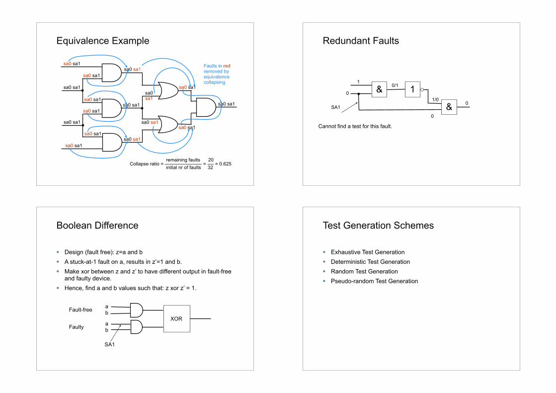
Equivalence Example
sa0 sa1sa0 sa1
sa0 sa1
sa0 sa1
sa0 sa1
sa0 sa1
sa0 sa1
sa0 sa1
sa0 sa1
sa0 sa1
sa0 sa1
sa0 sa1
sa0 sa1
sa0 sa1
sa0 sa1
sa0 sa1
Faults in redremoved byequivalencecollapsing
remaining faults 20Collapse ratio = ----------------------- = ---- = 0.625 initial nr of faults 32
Redundant Faults
SA1
&
&
10
0
10/1
1/00
Cannot find a test for this fault.
Boolean Difference
! Design (fault free): z=a and b! A stuck-at-1 fault on a, results in z’=1 and b. ! Make xor between z and z’ to have different output in fault-free
and faulty device. ! Hence, find a and b values such that: z xor z’ = 1.
XOR
ab
ab
Fault-free
Faulty
SA1
Test Generation Schemes
! Exhaustive Test Generation! Deterministic Test Generation! Random Test Generation! Pseudo-random Test Generation
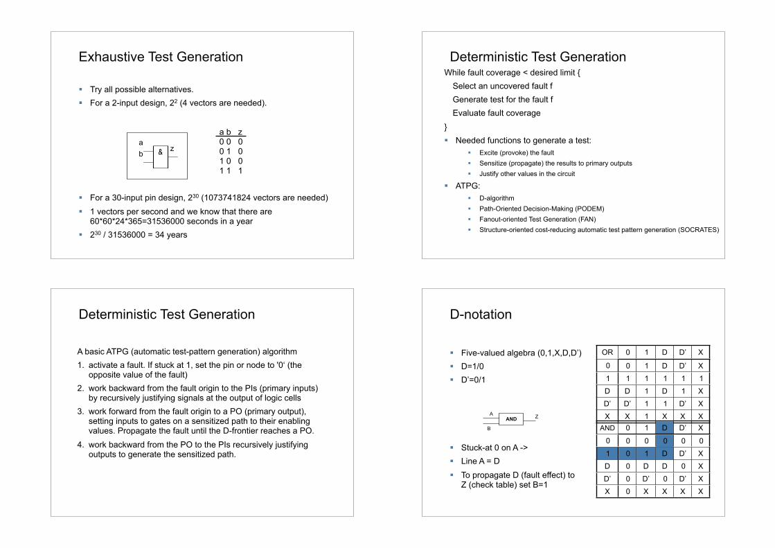
Exhaustive Test Generation
! Try all possible alternatives. ! For a 2-input design, 22 (4 vectors are needed).
! For a 30-input pin design, 230 (1073741824 vectors are needed)! 1 vectors per second and we know that there are
60*60*24*365=31536000 seconds in a year! 230 / 31536000 = 34 years
ab
z
a b z0 0 00 1 01 0 01 1 1
Deterministic Test GenerationWhile fault coverage < desired limit {
Select an uncovered fault fGenerate test for the fault fEvaluate fault coverage
}! Needed functions to generate a test:
! Excite (provoke) the fault! Sensitize (propagate) the results to primary outputs! Justify other values in the circuit
! ATPG: ! D-algorithm! Path-Oriented Decision-Making (PODEM)! Fanout-oriented Test Generation (FAN)! Structure-oriented cost-reducing automatic test pattern generation (SOCRATES)
Deterministic Test Generation
A basic ATPG (automatic test-pattern generation) algorithm 1. activate a fault. If stuck at 1, set the pin or node to '0‘ (the
opposite value of the fault) 2. work backward from the fault origin to the PIs (primary inputs)
by recursively justifying signals at the output of logic cells 3. work forward from the fault origin to a PO (primary output),
setting inputs to gates on a sensitized path to their enabling values. Propagate the fault until the D-frontier reaches a PO.
4. work backward from the PO to the PIs recursively justifying outputs to generate the sensitized path.
D-notation
! Five-valued algebra (0,1,X,D,D’)! D=1/0 ! D’=0/1
! Stuck-at 0 on A ->! Line A = D! To propagate D (fault effect) to
Z (check table) set B=1
OR 0 1 D D’ X
0 0 1 D D’ X
1 1 1 1 1 1
D D 1 D 1 X
D’ D’ 1 1 D’ X
X X 1 X X XAND 0 1 D D’ X
0 0 0 0 0 0
1 0 1 D D’ X
D 0 D D 0 X
D’ 0 D’ 0 D’ X
X 0 X X X X
ANDA
B
Z
D-AlgorithmOR
NORA
Z
BAND
NOR
AND
UW
X
Y
F
H
G
Stuck-at 0
G1G2
G3
G4
G5
! Initialize the circuit by placing X on each line! For a SA0, X=D and A=B=0 (for the selected fault)! Propagate D through G2! Select a sensitizing path (we select G3)! To propagate through G3, we let U=0! Propagate through G5! Reached a primary output with D! Justify values on H, Y, U, W. H=0 (ok). F=0? Conflict! Select Y=0
D-AlgorithmOR
NORA
Z
BAND
NOR
AND
UW
X
Y
F
H
G
Stuck-at 0
1 Operation Gate A B X Y W U F G H Z
2 Initialization x x x x x x x x x x
3 Provoke G1 0 0 D x x x x x x x
4 D-drive G2 0 0 D x 1 x D x x x
5 D-drive G3 0 0 D x 1 0 D D’ x x
6 D-drive G5 0 0 D x 1 0 D D’ 0 D’
7 Justification H=0 0 0 D x 1 0 ! D’ 0 D’
8 Justification H=0 0 0 D 0 1 0 D D’ 0 D’
G1G2
G3
G4
G5
! D=1/0
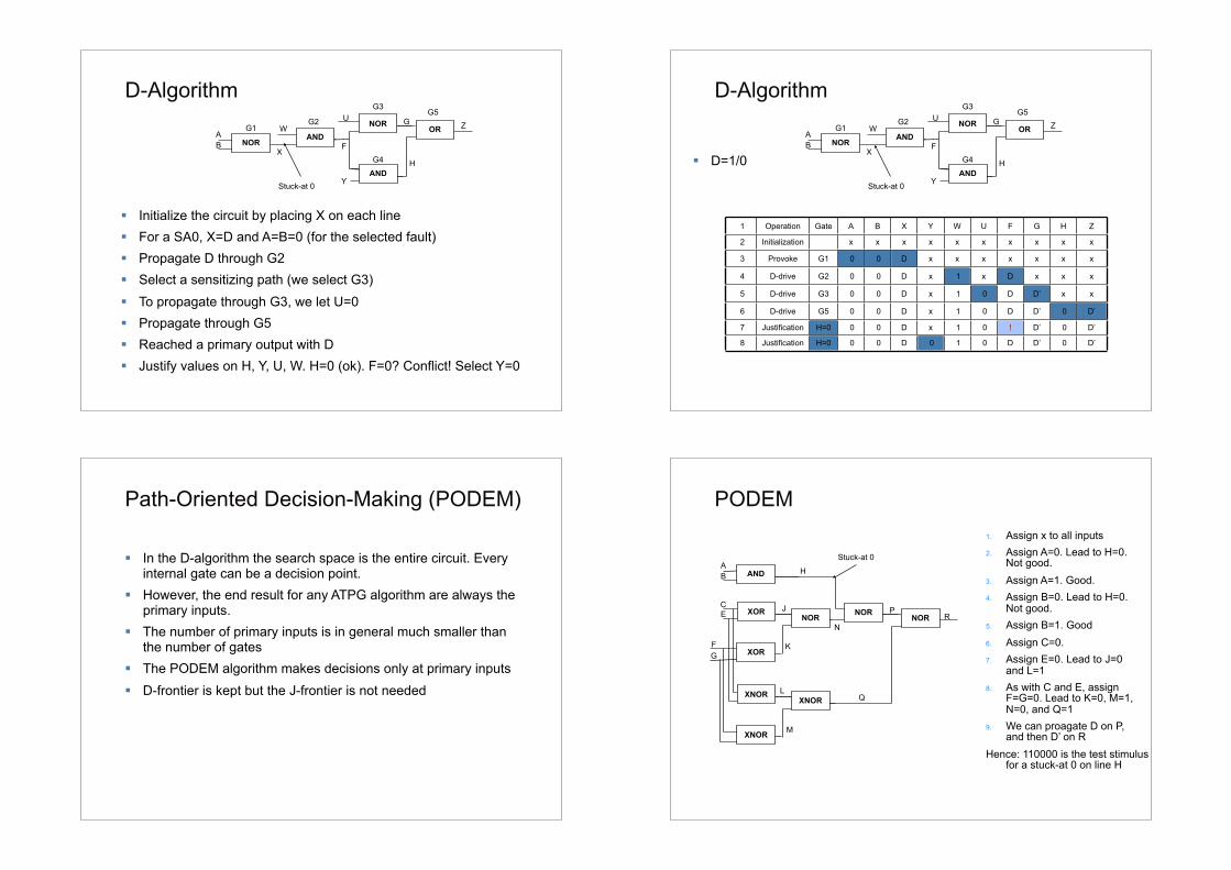
Path-Oriented Decision-Making (PODEM)
! In the D-algorithm the search space is the entire circuit. Every internal gate can be a decision point.
! However, the end result for any ATPG algorithm are always the primary inputs.
! The number of primary inputs is in general much smaller than the number of gates
! The PODEM algorithm makes decisions only at primary inputs! D-frontier is kept but the J-frontier is not needed
PODEM
XOR
XNOR
NORNOR
A
R
B
XNOR
XORNOR
AND
XNOR
CE
FG
H
J
K
L
M
N
Q
P
Stuck-at 0
1. Assign x to all inputs2. Assign A=0. Lead to H=0.
Not good. 3. Assign A=1. Good. 4. Assign B=0. Lead to H=0.
Not good.5. Assign B=1. Good6. Assign C=0. 7. Assign E=0. Lead to J=0
and L=18. As with C and E, assign
F=G=0. Lead to K=0, M=1, N=0, and Q=1
9. We can proagate D on P, and then D’ on R
Hence: 110000 is the test stimulusfor a stuck-at 0 on line H
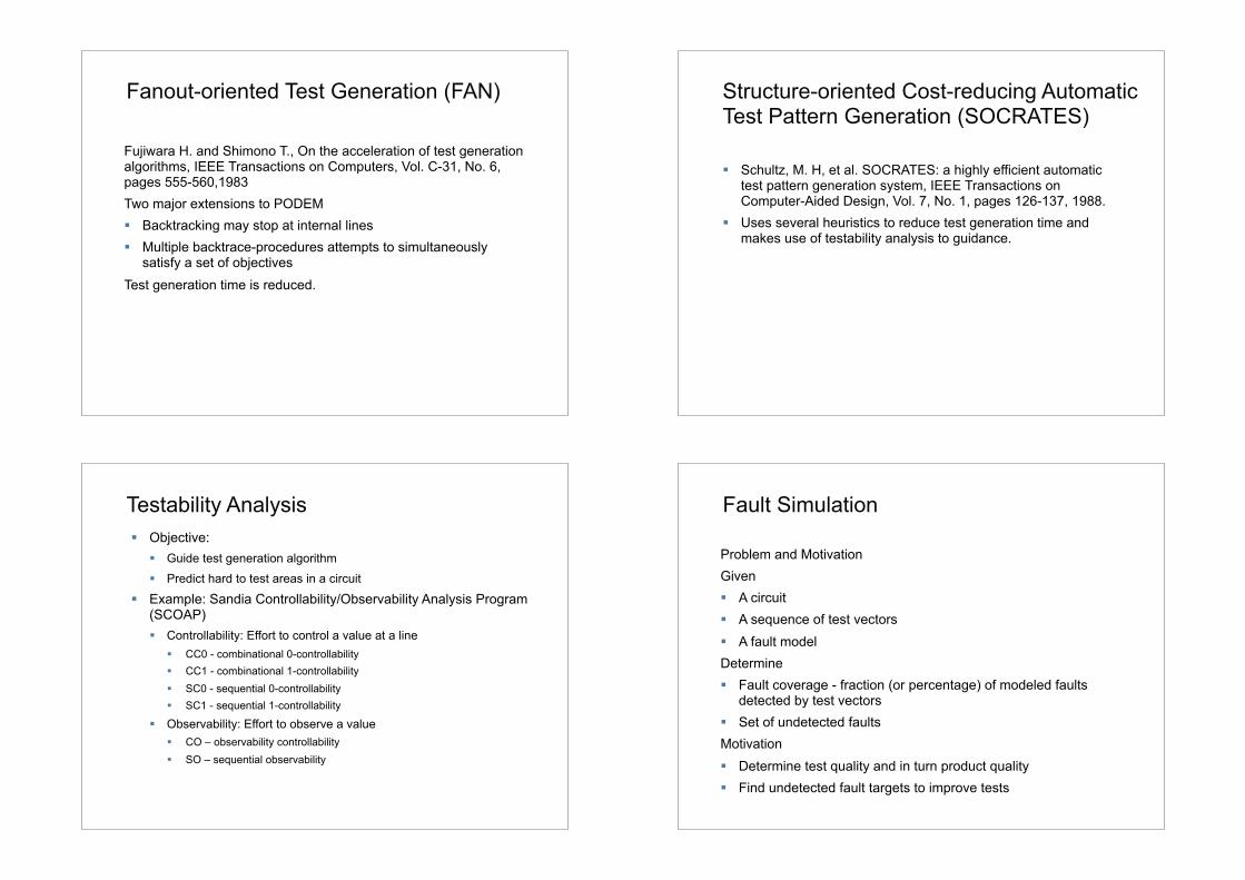
Fanout-oriented Test Generation (FAN)
Fujiwara H. and Shimono T., On the acceleration of test generation algorithms, IEEE Transactions on Computers, Vol. C-31, No. 6, pages 555-560,1983 Two major extensions to PODEM! Backtracking may stop at internal lines! Multiple backtrace-procedures attempts to simultaneously
satisfy a set of objectivesTest generation time is reduced.
Structure-oriented Cost-reducing Automatic Test Pattern Generation (SOCRATES)
! Schultz, M. H, et al. SOCRATES: a highly efficient automatic test pattern generation system, IEEE Transactions on Computer-Aided Design, Vol. 7, No. 1, pages 126-137, 1988.
! Uses several heuristics to reduce test generation time and makes use of testability analysis to guidance.
Testability Analysis! Objective:
! Guide test generation algorithm
! Predict hard to test areas in a circuit
! Example: Sandia Controllability/Observability Analysis Program (SCOAP)! Controllability: Effort to control a value at a line
! CC0 - combinational 0-controllability! CC1 - combinational 1-controllability! SC0 - sequential 0-controllability! SC1 - sequential 1-controllability
! Observability: Effort to observe a value! CO – observability controllability! SO – sequential observability
Fault Simulation
Problem and MotivationGiven! A circuit! A sequence of test vectors! A fault modelDetermine! Fault coverage - fraction (or percentage) of modeled faults
detected by test vectors! Set of undetected faultsMotivation! Determine test quality and in turn product quality! Find undetected fault targets to improve tests

Fault Simulation! Fault simulation consists of a fault free and a faulty circuit
simulation. ! First, a fault free simulation takes place to find the fault free
output responses for all patterns. ! Second, a series of simulations take place where. For each
fault, fault injection is performed, the circuit is modified to become faulty. Then, the faulty circuit is simulated to find the faulty responses.
NORAND K
OR
NOT
A
F
HG1
G2
G3
G4
BC E
InputInputInput InternalInternalInternal OutputOutputOutput
Pattern A B C E F H Kgood KSA1_A KSA0_F
P1 0 1 0 1 0 0 1 0 1
P2 0 0 1 1 0 0 1 0 1
P3 1 0 0 0 1 0 0 0 1
SA1
SA0
Fault Table - Analysis
! Fault simulator may provide fault table (fault dictionary)
FaultFaultFaultFaultFaultFaultFaultFaultFault
Pattern 1 2 3 4 5 6 7 8
1 x x x
2 x x x
3 x x x
4 x x x
Test Set Compaction
! ATPG generates too many vectors; faults are covered by several vectors
! Test set compaction tries to reduce number of test vectors without compromising test quality
! Static test set compaction tries to remove vectors after the use of ATPG
! Dynamic test tries to remove vectors during ATPG
f1 f2 f3 f4 f5 f6 f7v1 x x x
v2 x x
v3 x x x
v4 x x x x
Commercial ATPG Tools
! Commercial ATPG tools are often for combinational circuits! Commercial tools usually make use of a random test generation
for 60-80% of the faults (easy to detect) and deterministic test generation for the remaining part (hard to detect)
! Examples of commercial ATPG tools: ! Encounter Test - Cadence ! TetraMax - Synopsis
! FastScan, FlexTest - Mentor Graphics
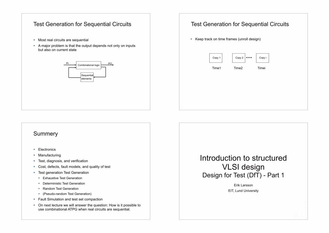
Test Generation for Sequential Circuits
! Most real circuits are sequential! A major problem is that the output depends not only on inputs
but also on current state
Combinational logicPI PO
Sequential elements
Test Generation for Sequential Circuits
! Keep track on time frames (unroll design)
Copy 1 Copy 2 Copy i
Time1 Time2 Timei
Summery
! Electronics! Manufacturing! Test, diagnosis, and verification! Cost, defects, fault models, and quality of test! Test generation Test Generation
! Exhaustive Test Generation
! Deterministic Test Generation! Random Test Generation! (Pseudo-random Test Generation)
! Fault Simulation and test set compaction! On next lecture we will answer the question: How is it possible to
use combinational ATPG when real circuits are sequential.
Introduction to structured VLSI design
Design for Test (DfT) - Part 1Erik Larsson
EIT, Lund University