Embed Size (px)
Citation preview

© 1996/2000. Montrose, M.I., Printed Circuit Board Design Techniques for EMC Compliance. Wiley/IEEE Press.© 1999. Montrose, M.I., EMC and the Printed Circuit Board - Design Theory and Layout Made Simple. Wiley/IEEE Press.
Introduction to Printed Circuit Board Design
For EMC Compliance
Mark MontrosePrinciple Consultant
Montrose Compliance Services, Inc.+ 1 (408) 247-5715
1

© 1996/2000. Montrose, M.I., Printed Circuit Board Design Techniques for EMC Compliance. Wiley/IEEE Press.© 1999. Montrose, M.I., EMC and the Printed Circuit Board - Design Theory and Layout Made Simple. Wiley/IEEE Press.
Fundamentals of Signal Integrity
2
© 1996/2000. Montrose, M.I., Printed Circuit Board Design Techniques for EMC Compliance. Wiley/IEEE Press.© 1999. Montrose, M.I., EMC and the Printed Circuit Board - Design Theory and Layout Made Simple. Wiley/IEEE Press.
What is Signal Integrity
The ability of electrical signals to travel from a source to load through a dielectric without loss of signal amplitude or parametric values
In order to solve a signal integrity problem, one must first understand transmission lines and how they function both in theory and reality
There are two kinds of design engineers:“Those that have signal integrity problems, and those that will”
3

Signal Integrity Concerns
It only takes one item listed below to cause a signal integrity problem
• Incorrect transmission line routing• Improper terminations• Power and/or return plane bounce• Improper RF return current path• Mode conversion• Rise time degradation• Lossy transmission lines at higher
frequencies• Poor power distribution network• Hidden parasitics (RLC)• Propagation delays• Skin depth and dielectric loss• Non-monotonic edges• Excessive inductance in the
transmission line• Excessive ringing and reflection• Lossy transmission lines• Poor printed circuit board material
• Overshoot and undershoot• Impedance discontinuities• Delta I noise• RC delay• Crosstalk• Stubs and their lengths• Excessive capacitive loaded lines• IR drops• Via stubs• Excess attenuation• Non-monotonic edges• Signal skew• Gaps in planes• Dispersion• Impedance discontinuities• Unknown parasitic• Intra line skew• High dielectric losses
© 1996/2000. Montrose, M.I., Printed Circuit Board Design Techniques for EMC Compliance. Wiley/IEEE Press.© 1999. Montrose, M.I., EMC and the Printed Circuit Board - Design Theory and Layout Made Simple. Wiley/IEEE Press.
4
© 1996/2000. Montrose, M.I., Printed Circuit Board Design Techniques for EMC Compliance. Wiley/IEEE Press.© 1999. Montrose, M.I., EMC and the Printed Circuit Board - Design Theory and Layout Made Simple. Wiley/IEEE Press.
Aspects of High-Speed Problems
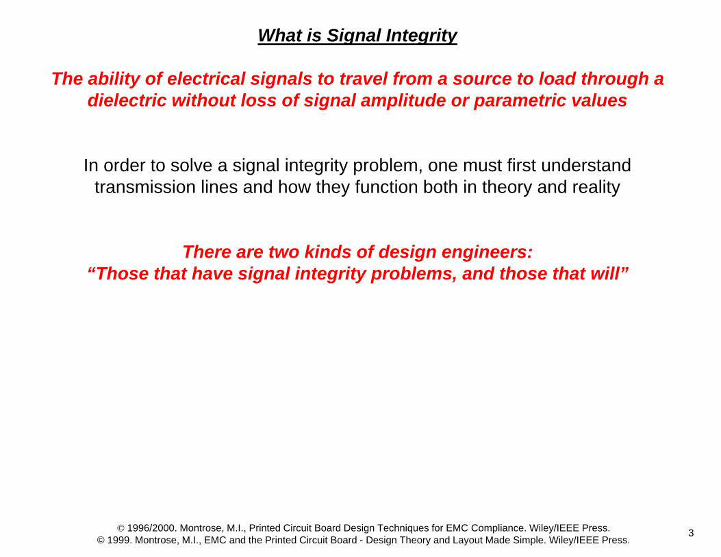
Four aspects of high-speed problems are present in system designs
1. Signal quality: Reflections and distortions from impedance discontinuities in the signal or return path can affect the quality of the signal. A transmitted signal should see the same impedance throughout all interconnects (includes vias and connectors).
2. Crosstalk between nets: Mutual capacitance and inductance exists, both within an ideal and non-ideal return path. One must keep spacing of traces greater than a minimal value while minimizing mutual inductance, keeping the return path impedance as low as possible.
3. Rail collapse: A voltage drop within the power and return system when digital components switch logic states. One must minimize the impedance of the power and return path along with the delta-I (current).
4. EMI: Can be developed as a result of poor signal integrity within a transmission line. Must minimize bandwidth, ground impedance and common-mode coupling.
Details on impedance discontinuities, transmission line routing, terminations, and simulations are presented later.
5

© 1996/2000. Montrose, M.I., Printed Circuit Board Design Techniques for EMC Compliance. Wiley/IEEE Press.© 1999. Montrose, M.I., EMC and the Printed Circuit Board - Design Theory and Layout Made Simple. Wiley/IEEE Press.
totaltotalpdo
oo CLt
I(x)V(x) =
CL = Z
Lossless Transmission Line Equivalent Circuit Within a PCB
6
© 1996/2000. Montrose, M.I., Printed Circuit Board Design Techniques for EMC Compliance. Wiley/IEEE Press.© 1999. Montrose, M.I., EMC and the Printed Circuit Board - Design Theory and Layout Made Simple. Wiley/IEEE Press.
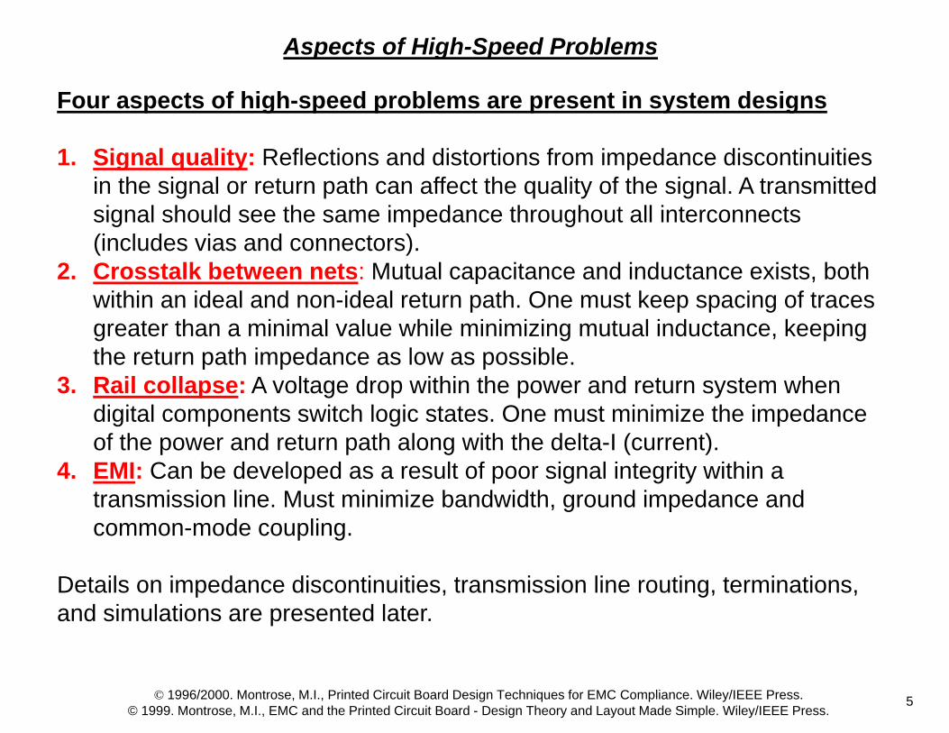
Lossy Transmission Line Equivalent Circuit Within a PCB
CjGLjRj LLLL
CjGLjRZo
LL
LL
characteristic impedanceZo
lengthlineLmay vary with frequencyG,R LL
jtxVxV o )exp()exp(),(
7

© 1996/2000. Montrose, M.I., Printed Circuit Board Design Techniques for EMC Compliance. Wiley/IEEE Press.© 1999. Montrose, M.I., EMC and the Printed Circuit Board - Design Theory and Layout Made Simple. Wiley/IEEE Press.
Lossy Transmission Lines
1. Resistive losses - Constant with frequency. Attenuation, usually measured in dB/unit distance, is proportional to the resistance per unit length of the conductor.
2. Skin effect losses - Proportional to the square root of frequency. As signal frequency increases, current flow retreats to the surface of the conductor flowing in a "skin" which becomes thinner with increasing frequency. Resistivity of the material stays the same, it is the cross section that decreases related to AC current flow.
3. Dielectric losses - The PCB material (core and prepreg) absorbs some of the electric field energy, which is directly proportional to frequency. Dielectric loss or dissipation factor (magnitude of energy loss) is not the same as dielectric constant (speed of signal travel).
4. Resonances - Typically caused by improperly terminated traces and split planes in addition to the lumped magnitude of both capacitance and inductance within power distribution networks.
8
© 1996/2000. Montrose, M.I., Printed Circuit Board Design Techniques for EMC Compliance. Wiley/IEEE Press.© 1999. Montrose, M.I., EMC and the Printed Circuit Board - Design Theory and Layout Made Simple. Wiley/IEEE Press.
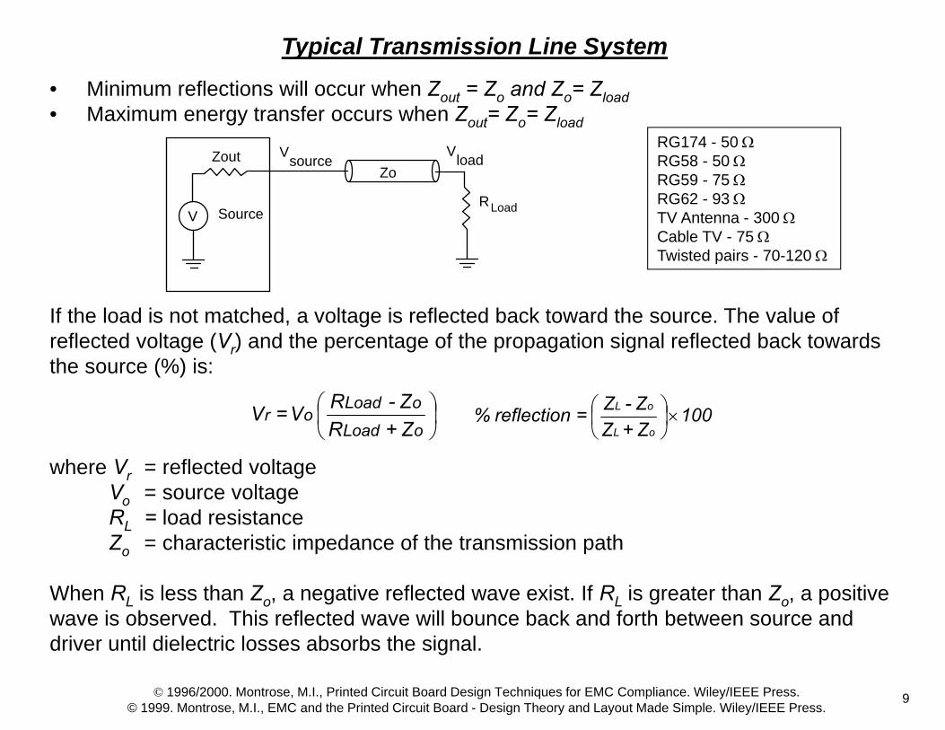
Typical Transmission Line System
• Minimum reflections will occur when Zout = Zo and Zo= Zload• Maximum energy transfer occurs when Zout= Zo= Zload
If the load is not matched, a voltage is reflected back toward the source. The value of reflected voltage (Vr) and the percentage of the propagation signal reflected back towards the source (%) is:
where Vr = reflected voltageVo = source voltageRL = load resistanceZo = characteristic impedance of the transmission path
When RL is less than Zo, a negative reflected wave exist. If RL is greater than Zo, a positive wave is observed. This reflected wave will bounce back and forth between source and driver until dielectric losses absorbs the signal.
Zo
V Source
Zout
RLoad
VloadVsource
oLoad
oLoad or
Z+RZ-RV = V 100
Z+ZZ-Z =reflection %
oL
oL
RG174 - 50 RG58 - 50 RG59 - 75 RG62 - 93 TV Antenna - 300 Cable TV - 75 Twisted pairs - 70-120
9
© 1996/2000. Montrose, M.I., Printed Circuit Board Design Techniques for EMC Compliance. Wiley/IEEE Press.© 1999. Montrose, M.I., EMC and the Printed Circuit Board - Design Theory and Layout Made Simple. Wiley/IEEE Press.
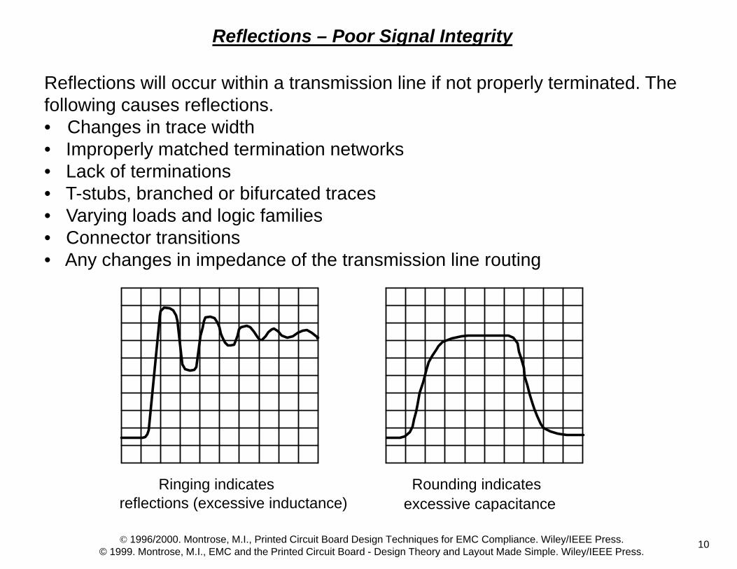
Reflections – Poor Signal Integrity
Reflections will occur within a transmission line if not properly terminated. The following causes reflections.• Changes in trace width• Improperly matched termination networks• Lack of terminations• T-stubs, branched or bifurcated traces• Varying loads and logic families• Connector transitions• Any changes in impedance of the transmission line routing
Ringing indicates Rounding indicatesexcessive capacitancereflections (excessive inductance)
10
© 1996/2000. Montrose, M.I., Printed Circuit Board Design Techniques for EMC Compliance. Wiley/IEEE Press.© 1999. Montrose, M.I., EMC and the Printed Circuit Board - Design Theory and Layout Made Simple. Wiley/IEEE Press.
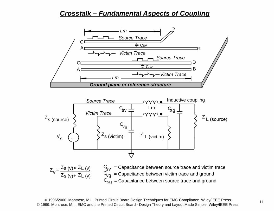
Crosstalk – Fundamental Aspects of Coupling
Zv = Zs (v)x ZL (v)Zs (v) ZL (v)+
Source Trace
Victim Trace
Victim Trace
Source TraceLm
Csv
CsvCvg
= Capacitance between source trace and victim trace= Capacitance between victim trace and ground
Csg = Capacitance between source trace and ground
Source Trace
Victim TraceCsv
Cvg
Z L (source)
Z L (victim)~
Zs (source)
VsZs (victim)
Inductive coupling
Csg
Ground plane or reference structureLm
Csv
AC
CA
B
B
D
D
Lm
11

© 1996/2000. Montrose, M.I., Printed Circuit Board Design Techniques for EMC Compliance. Wiley/IEEE Press.© 1999. Montrose, M.I., EMC and the Printed Circuit Board - Design Theory and Layout Made Simple. Wiley/IEEE Press.
Vs
Rs Ls
Rv Lv
Zg
Csg
Cvg
Z ZL1
L2Z
s1
Vv
Zs2
G (0V)
Schematic representation of a three wire circuit
MsvCsv
CsvCvg
= Capacitance between source trace and victim trace= Capacitance between victim trace and ground
Csg = Capacitance between source trace and ground
ZL1 ZL2
Csv
Msv
Vs
Zs1
Vv
Z s2
G (0V)
t
VsSource signal
t
Vv
Crosstalk onvictim trace
CvgCsg
Zg
Vs VvZs1 Zs2
ZL1 ZL2
Ground plane
Dielectric
Parallel traces over a ground plane
G (0V)
material
12

13
Stuck low
Coupled lines
Agressor line
Victim line
0.000 4.000 8.000 12.000 16.000 20.000Time (ns)
Voltage -V-
-3.000
-2.000
-1.000
0.000
1.000
2.000
3.000
4.000
5.000
6.000
7.000
Agressor line (source) - clock stimulus
Agressor line (load)
Victim line (source) - stuck lowVictim line (load)
0.010"
0.010"
0.010"
Signal
Power
Ground
Signal
0.008 0.008 0.0088.0 inches (20.3 cm) long, 72.1 ohmsPropagational delay: 1.126 nsOscillator: 66 MHz, 49% duty cycleCMOS, 3.3V, FastTraces: 0.008" wide and 0.008" apart (.20mm)Distance to reference plane: 0.010" (.25mm)
© 1996/2000. Montrose, M.I., Printed Circuit Board Design Techniques for EMC Compliance. Wiley/IEEE Press.© 1999. Montrose, M.I., EMC and the Printed Circuit Board - Design Theory and Layout Made Simple. Wiley/IEEE Press.
© 1996/2000. Montrose, M.I., Printed Circuit Board Design Techniques for EMC Compliance. Wiley/IEEE Press.© 1999. Montrose, M.I., EMC and the Printed Circuit Board - Design Theory and Layout Made Simple. Wiley/IEEE Press.
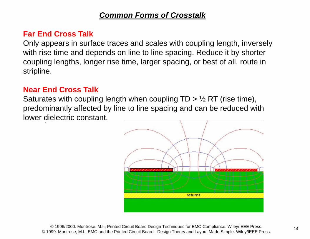
Far End Cross TalkOnly appears in surface traces and scales with coupling length, inversely with rise time and depends on line to line spacing. Reduce it by shorter coupling lengths, longer rise time, larger spacing, or best of all, route in stripline.
Near End Cross TalkSaturates with coupling length when coupling TD > ½ RT (rise time), predominantly affected by line to line spacing and can be reduced with lower dielectric constant..
Common Forms of Crosstalk
14

© 1996/2000. Montrose, M.I., Printed Circuit Board Design Techniques for EMC Compliance. Wiley/IEEE Press.© 1999. Montrose, M.I., EMC and the Printed Circuit Board - Design Theory and Layout Made Simple. Wiley/IEEE Press.
Sample List of Design Techniques to Prevent Crosstalk
To prevent crosstalk within a PCB, the following design and layout techniques are useful.• Crosstalk will increase with a wider trace width as mutual capacitance, Cm, increases.• With long parallel traces, greater mutual inductance, Lm, is present. • Crosstalk also increases with faster edge rates and frequency of operation.
1. Group logic devices according to functionality. 2. Minimize routed distance between components.3. Minimize parallel routed trace lengths.4. Locate components away from I/O interconnects and areas susceptible to field
corruption.5. Provide terminations for traces rich in harmonic energy.6. Avoid routing of traces parallel to each other with adequate separation between the
tracks.7. Route adjacent signal layers (either microstrip or stripline) orthogonally to prevents
capacitive and inductive coupling between two planes in parallel.8. Reduce signal-to-ground reference distance separation.9. Reduce trace impedance and/or signal drive level.10. Isolate signal layers routed in the same axis by a solid planar (typical of backplane
designs).
15

© 1996/2000. Montrose, M.I., Printed Circuit Board Design Techniques for EMC Compliance. Wiley/IEEE Press.© 1999. Montrose, M.I., EMC and the Printed Circuit Board - Design Theory and Layout Made Simple. Wiley/IEEE Press.
Power and/or Return Plane Bounce
dtdIL = V discharge
rnpower/returnpower/retu
16

© 1996/2000. Montrose, M.I., Printed Circuit Board Design Techniques for EMC Compliance. Wiley/IEEE Press.© 1999. Montrose, M.I., EMC and the Printed Circuit Board - Design Theory and Layout Made Simple. Wiley/IEEE Press.
Fundamentals of EMC
17

© 1996/2000. Montrose, M.I., Printed Circuit Board Design Techniques for EMC Compliance. Wiley/IEEE Press.© 1999. Montrose, M.I., EMC and the Printed Circuit Board - Design Theory and Layout Made Simple. Wiley/IEEE Press.
Component Characteristics at RF Frequencies(The Hidden Schematic)
18
© 1996/2000. Montrose, M.I., Printed Circuit Board Design Techniques for EMC Compliance. Wiley/IEEE Press.© 1999. Montrose, M.I., EMC and the Printed Circuit Board - Design Theory and Layout Made Simple. Wiley/IEEE Press.
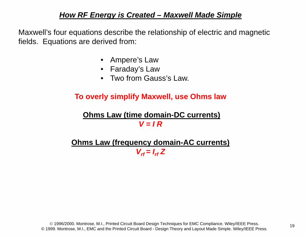
How RF Energy is Created – Maxwell Made Simple
Maxwell’s four equations describe the relationship of electric and magnetic fields. Equations are derived from:
• Ampere’s Law• Faraday’s Law• Two from Gauss’s Law.
To overly simplify Maxwell, use Ohms law
Ohms Law (time domain-DC currents)V = I R
Ohms Law (frequency domain-AC currents)Vrf = Irf Z
19

© 1996/2000. Montrose, M.I., Printed Circuit Board Design Techniques for EMC Compliance. Wiley/IEEE Press.© 1999. Montrose, M.I., EMC and the Printed Circuit Board - Design Theory and Layout Made Simple. Wiley/IEEE Press.
Right Hand Rule(Faraday’s Law)
Field or Flux Line
I (Current in the wire)
(Magnetic Flux)
20

© 1996/2000. Montrose, M.I., Printed Circuit Board Design Techniques for EMC Compliance. Wiley/IEEE Press.© 1999. Montrose, M.I., EMC and the Printed Circuit Board - Design Theory and Layout Made Simple. Wiley/IEEE Press.
Maxwell's Equations(For Reference Purposes)
totals
s
s
vs
I dst D JdlH
t D + J = H
Ampere) (from Current Electric :Law Fourth
dst B - = dlE
t B - = E
Faraday) (from Potential Electric :Law Third
0 dsB 0 B
Gauss) (from Flux Magnetic :Law Second
0 dv dsD = D
Gauss) (from Flux Electric :Law First
m
e
21

Electric and Magnetic Field Impedance
A plane wave is a combination of both electric and magnetic field components (Poynting vector). Fields propagate from a field source near the velocity of light.
where o = 410-7 H/m o = 8.8510-12 F/m
Electric field component is measured in volts/meter (Note-voltage)Magnetic field component is in amps/meter (Note-current)
The ratio of both electric field (E) to magnetic field (H) is identified as the "impedance" of free space. This impedance ratio is described by:
Energy carried in the wave front is measured in Watts/meter2 (Note-power)
© 1996/2000. Montrose, M.I., Printed Circuit Board Design Techniques for EMC Compliance. Wiley/IEEE Press.© 1999. Montrose, M.I., EMC and the Printed Circuit Board - Design Theory and Layout Made Simple. Wiley/IEEE Press.
8oo 10 x3 = 1/=c
ohms 377 = εμ = HE =Z
o
o o
22
(Note-resistance)

© 1996/2000. Montrose, M.I., Printed Circuit Board Design Techniques for EMC Compliance. Wiley/IEEE Press.© 1999. Montrose, M.I., EMC and the Printed Circuit Board - Design Theory and Layout Made Simple. Wiley/IEEE Press.
23
d1H
dE
1
3d1H
dE 2
1
2d1H
dE 3
1

© 1996/2000. Montrose, M.I., Printed Circuit Board Design Techniques for EMC Compliance. Wiley/IEEE Press.© 1999. Montrose, M.I., EMC and the Printed Circuit Board - Design Theory and Layout Made Simple. Wiley/IEEE Press.
Electric and Magnetic Field Representation
Dipole Antenna Loop Antenna
24

© 1996/2000. Montrose, M.I., Printed Circuit Board Design Techniques for EMC Compliance. Wiley/IEEE Press.© 1999. Montrose, M.I., EMC and the Printed Circuit Board - Design Theory and Layout Made Simple. Wiley/IEEE Press.
Closed Loop Circuit
If a continuous, conductive low impedance RF return path is not present(transmission line impedance is greater than 377 ohms), the return path will befree space (377 at /4), which may be much less than the impedance of alocalized RF return path.
Signal path
Return path
Switch
25

© 1996/2000. Montrose, M.I., Printed Circuit Board Design Techniques for EMC Compliance. Wiley/IEEE Press.© 1999. Montrose, M.I., EMC and the Printed Circuit Board - Design Theory and Layout Made Simple. Wiley/IEEE Press.
Radiated Emissions from a Closed Loop Circuit
Loop Area
Radiated energy
Return current
Signal path
26
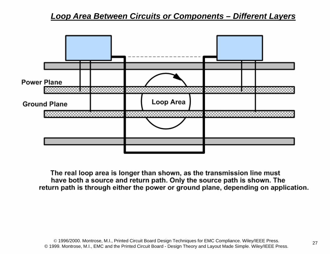
Loop Area Between Circuits or Components – Different Layers
© 1996/2000. Montrose, M.I., Printed Circuit Board Design Techniques for EMC Compliance. Wiley/IEEE Press.© 1999. Montrose, M.I., EMC and the Printed Circuit Board - Design Theory and Layout Made Simple. Wiley/IEEE Press.
27
© 1996/2000. Montrose, M.I., Printed Circuit Board Design Techniques for EMC Compliance. Wiley/IEEE Press.© 1999. Montrose, M.I., EMC and the Printed Circuit Board - Design Theory and Layout Made Simple. Wiley/IEEE Press.
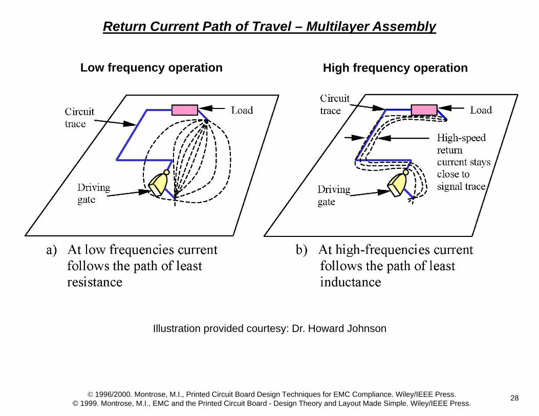
Return Current Path of Travel – Multilayer Assembly
High frequency operationLow frequency operation
Illustration provided courtesy: Dr. Howard Johnson
28

Circuit Return Current Simulation @ F=1 Hz Circuit Return Current Simulation @ F=100 kHz
Circuit Return Current Simulation @ F=5 GHz
Courtesy of Alexander Perez, Agilent Technologies
© 1996/2000. Montrose, M.I., Printed Circuit Board Design Techniques for EMC Compliance. Wiley/IEEE Press.© 1999. Montrose, M.I., EMC and the Printed Circuit Board - Design Theory and Layout Made Simple. Wiley/IEEE Press.
29

© 1996/2000. Montrose, M.I., Printed Circuit Board Design Techniques for EMC Compliance. Wiley/IEEE Press.© 1999. Montrose, M.I., EMC and the Printed Circuit Board - Design Theory and Layout Made Simple. Wiley/IEEE Press.
Common-Mode and Differential-Mode Currents
Differential-mode1. Conveys desired information.2. Does not cause interference as the fields generated oppose each other and cancel out.
Common-mode1. The major source of cable radiation.2. Contains no useful information.3. Has no useful purpose.4. Causes a system (traces, cables, etc.) to radiate as a monopole antenna.
I1
E~
I2
Z~
Noise sourcein load
I2
Common-mode currentI = I 1 + I2total
Differential-mode currentI = I 1 - I2total
E~ Z
Noise sourcein loadI1
~+ +
I2'
2 2
½ CM½ DM
½ CM½ DM
30
© 1996/2000. Montrose, M.I., Printed Circuit Board Design Techniques for EMC Compliance. Wiley/IEEE Press.© 1999. Montrose, M.I., EMC and the Printed Circuit Board - Design Theory and Layout Made Simple. Wiley/IEEE Press.
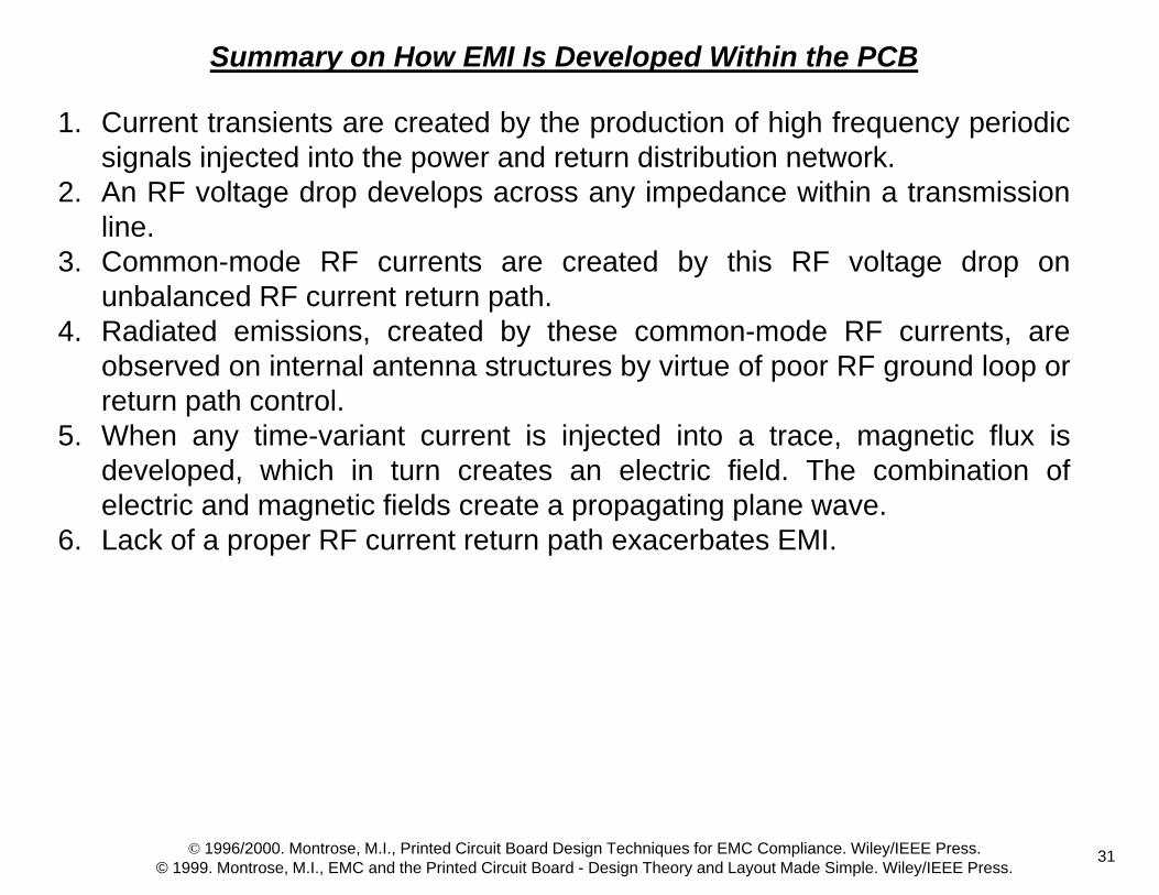
Summary on How EMI Is Developed Within the PCB
1. Current transients are created by the production of high frequency periodicsignals injected into the power and return distribution network.
2. An RF voltage drop develops across any impedance within a transmissionline.
3. Common-mode RF currents are created by this RF voltage drop onunbalanced RF current return path.
4. Radiated emissions, created by these common-mode RF currents, areobserved on internal antenna structures by virtue of poor RF ground loop orreturn path control.
5. When any time-variant current is injected into a trace, magnetic flux isdeveloped, which in turn creates an electric field. The combination ofelectric and magnetic fields create a propagating plane wave.
6. Lack of a proper RF current return path exacerbates EMI.
31

© 1996/2000. Montrose, M.I., Printed Circuit Board Design Techniques for EMC Compliance. Wiley/IEEE Press.© 1999. Montrose, M.I., EMC and the Printed Circuit Board - Design Theory and Layout Made Simple. Wiley/IEEE Press.
Basic EMC Suppression and Grounding Concepts
32
© 1996/2000. Montrose, M.I., Printed Circuit Board Design Techniques for EMC Compliance. Wiley/IEEE Press.© 1999. Montrose, M.I., EMC and the Printed Circuit Board - Design Theory and Layout Made Simple. Wiley/IEEE Press.
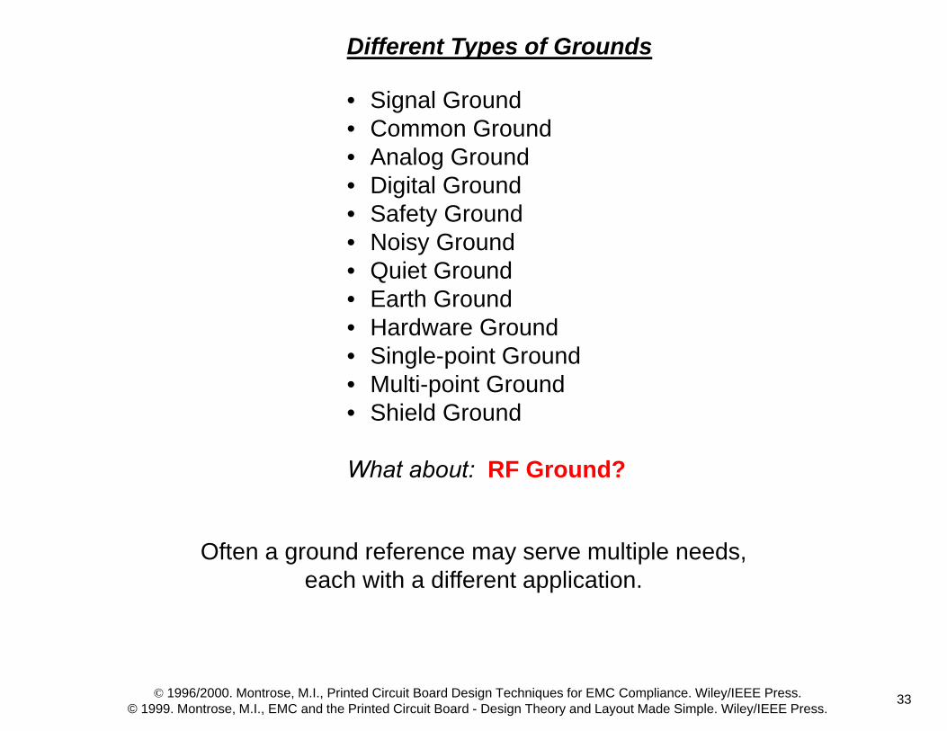
Different Types of Grounds
• Signal Ground• Common Ground• Analog Ground• Digital Ground• Safety Ground• Noisy Ground• Quiet Ground• Earth Ground• Hardware Ground• Single-point Ground• Multi-point Ground• Shield Ground
What about: RF Ground?
Often a ground reference may serve multiple needs, each with a different application.
33

Defining “Ground”
Power/safety ground• Intended (neutral) and unintended (safety ground, generally the green wire)• 50/60/400 Hz
Lightning ground• A controlled path for lightning to reach the earth through a rod or metallic
structure• Generally a 1 MHz event and up to 100 kAmps per millisecond• Requires a high quality low ground resistance and inductance
Circuit/signal ground• Provides a return path for intended signal flow and for AC/DC power return;
mA to Amps• Requires a minimum low impedance path• Generally implemented as a ground plane or grids within a printed circuit
board
© 1996/2000. Montrose, M.I., Printed Circuit Board Design Techniques for EMC Compliance. Wiley/IEEE Press.© 1999. Montrose, M.I., EMC and the Printed Circuit Board - Design Theory and Layout Made Simple. Wiley/IEEE Press.
34

Defining “Ground” (continued)
EMI ground• Provides a controlled path for RF currents; DC to daylight, A to Amps• Requires a minimum ground impedance
ESD ground• Provides a controlled path for ESD currents • 0.7-3 ns rise times, 100-300 MHz, 10-50 Amps
RF ground• Provides an RF return path for flux to return to its source• Covers the entire frequency spectrum• Requires minimum impedance for maximum current/flux flow
© 1996/2000. Montrose, M.I., Printed Circuit Board Design Techniques for EMC Compliance. Wiley/IEEE Press.© 1999. Montrose, M.I., EMC and the Printed Circuit Board - Design Theory and Layout Made Simple. Wiley/IEEE Press.
© 1996/2000. Montrose, M.I., Printed Circuit Board Design Techniques for EMC Compliance. Wiley/IEEE Press.© 1999. Montrose, M.I., EMC and the Printed Circuit Board - Design Theory and Layout Made Simple. Wiley/IEEE Press.
35

36
• A ground system topology is determined by– Signal characteristics– System dimensions– System-specific separation and isolation requirements– Electrical safety requirements
• Primary ground system topologies includes– A “floating” system– Single-point (“star) ground (SPG)– Multi-point ground– Hybrid ground
Grounding System Topologies
© 1996/2000. Montrose, M.I., Printed Circuit Board Design Techniques for EMC Compliance. Wiley/IEEE Press.© 1999. Montrose, M.I., EMC and the Printed Circuit Board - Design Theory and Layout Made Simple. Wiley/IEEE Press.

© 1996/2000. Montrose, M.I., Printed Circuit Board Design Techniques for EMC Compliance. Wiley/IEEE Press.© 1999. Montrose, M.I., EMC and the Printed Circuit Board - Design Theory and Layout Made Simple. Wiley/IEEE Press.
Three Primary Grounding Methodologies
Single-Point Grounding: Series and Parallel Multi-Point
37

© 1996/2000. Montrose, M.I., Printed Circuit Board Design Techniques for EMC Compliance. Wiley/IEEE Press.© 1999. Montrose, M.I., EMC and the Printed Circuit Board - Design Theory and Layout Made Simple. Wiley/IEEE Press.
Single-Point: Best for use when signals are below 1 MHz.• Most sensitive circuit returns should be connected closest to the final
equipotential point.• Provides for greatest amount of loop currents to flow.• May be used between 1 and 10 MHz if longest conductor is < /20 of a
wavelength of highest frequency generated in the system.• Divided into two type: series and parallel.
Multi-Point: Preferred for frequencies above 1 MHz.• Minimized loop currents and ground impedance of the planes. A good low
inductance ground is necessary for high-frequency digital logic circuits. Ground plane(s) provides a low inductance ground return for RF currents.
• Lead inductance must be kept extremely short.• Provides for maximum EMI suppression at the PCB level.
Hybrid: For mixed technology products.• A combination of both single-point and multi-point grounding in the same
system
38

© 1996/2000. Montrose, M.I., Printed Circuit Board Design Techniques for EMC Compliance. Wiley/IEEE Press.© 1999. Montrose, M.I., EMC and the Printed Circuit Board - Design Theory and Layout Made Simple. Wiley/IEEE Press.
Resonance in a Multi-Point Ground
Printed circuit board.
Mounting plate or chassisMounting posts
Eddy currents
Internal power plane capacitance
Inductance in the power planes
ZZ I cm
Vcmby eddy currentsacross impedance(Z)post.
LC resonance in mounting posts
from mounting
produced
APPLICATION MODEL OF MULTIPOINT GROUNDING
ZtZ t cm2Vcm2V
cmI
ZB
Vcm1
Chassis
ELECTROMAGNETIC MODEL OF MULTI-POINT GROUNDING
V cm2 is reduced by the mounting posts (ground stitch locations).Resonance is thus controlled, along with enhanced RF suppression.
39

© 1996/2000. Montrose, M.I., Printed Circuit Board Design Techniques for EMC Compliance. Wiley/IEEE Press.© 1999. Montrose, M.I., EMC and the Printed Circuit Board - Design Theory and Layout Made Simple. Wiley/IEEE Press.
RF Current Density Distribution
where I(d) = signal current density, (A/inch or A/cm)Io = total current (A)H = height of the trace above the ground plane (in. or cm)D = perpendicular distance from the center line of the trace (in. or cm)
21
1
HDH
I = dI o
)(
40

© 1996/2000. Montrose, M.I., Printed Circuit Board Design Techniques for EMC Compliance. Wiley/IEEE Press.© 1999. Montrose, M.I., EMC and the Printed Circuit Board - Design Theory and Layout Made Simple. Wiley/IEEE Press.
Ground Slots Created with Through-Hole Components
41

© 1996/2000. Montrose, M.I., Printed Circuit Board Design Techniques for EMC Compliance. Wiley/IEEE Press.© 1999. Montrose, M.I., EMC and the Printed Circuit Board - Design Theory and Layout Made Simple. Wiley/IEEE Press.
Functional Partitioning
Slow speed I/O
CPU and clock logic
interconnects
Memory
Video Audio
Memory section
Power supply
Adapter cardsSupport logic
Analog processing
42

© 1996/2000. Montrose, M.I., Printed Circuit Board Design Techniques for EMC Compliance. Wiley/IEEE Press.© 1999. Montrose, M.I., EMC and the Printed Circuit Board - Design Theory and Layout Made Simple. Wiley/IEEE Press.
Bypassing and Decoupling(Power Distribution Networks)
43

© 1996/2000. Montrose, M.I., Printed Circuit Board Design Techniques for EMC Compliance. Wiley/IEEE Press.© 1999. Montrose, M.I., EMC and the Printed Circuit Board - Design Theory and Layout Made Simple. Wiley/IEEE Press.
The Need for Optimal Power Distribution
• Provides a stable voltage reference between components to ensure functional operation
• Distribute optimal power to all logic devices to minimize planar bounce
Key items of concernUse low impedance connections between logic gates:• The impedance between power pins on gates should be just as low as the
impedance between the return pins on the same device• A low impedance path must always be provided between power and return
Input+
-
+
-
+
-
Load C
Inductance in the Power Path
Charging current for capacitor C flows throughthe inductance of the power distribution network
I
Signal
Inductance in the Return Path
44

© 1996/2000. Montrose, M.I., Printed Circuit Board Design Techniques for EMC Compliance. Wiley/IEEE Press.© 1999. Montrose, M.I., EMC and the Printed Circuit Board - Design Theory and Layout Made Simple. Wiley/IEEE Press.
Power Distribution Networks as Transmission Lines
Power distribution networks can be represented as a two conductor transmission line with a defined characteristic impedance and propagation delay.
45

© 1996/2000. Montrose, M.I., Printed Circuit Board Design Techniques for EMC Compliance. Wiley/IEEE Press.© 1999. Montrose, M.I., EMC and the Printed Circuit Board - Design Theory and Layout Made Simple. Wiley/IEEE Press.
Primary Requirements for Enhanced Power Distribution
The amplitude of power supply transients are directly proportional to the characteristic impedance of the power distribution system, Z0:
To reduce Z0
– Reduce inductance– Increase capacitance
Both are achieved by– Reduction of loop area between conductors (less inductance)– Placing conductors as close together as possible (greater capacitance)– Increase of conductors’ width (less inductance and greater capacitance,
with respect to another conductor)
(x)
(x)
o
oo
IV
CL = Z
46

© 1996/2000. Montrose, M.I., Printed Circuit Board Design Techniques for EMC Compliance. Wiley/IEEE Press.© 1999. Montrose, M.I., EMC and the Printed Circuit Board - Design Theory and Layout Made Simple. Wiley/IEEE Press.
Defining Capacitor Usage
Capacitors are used for one of three primary functions.
Bulk Used to maintain constant DC voltage and current levels on a global basis due to IR drops within the power distribution network, and to recharge the distribution network (i.e., planes) cause by dI/dt consumption from components (typically 1-100 F).
Bypassing Diverts or steers RF currents from one location to another. Shunts unwanted common-mode RF currents from components or cables from entering susceptible areas in addition to providing other functions of filtering (bandwidth limited).
Decoupling Provides a localized source of DC power, and are particularly useful in reducing peak current surges propagated across the board. Prevents RF currents from being injected into the power distribution network during digital component edge transitions.
• Switching transient capacitance (0.01 F) – Used to supply short-term energy demands of the silicon during switching states.
• Line charging capacitance (0.1 F) – Used to charge capacitive transmission lines as well as supplying current necessary for the driver.
47

© 1996/2000. Montrose, M.I., Printed Circuit Board Design Techniques for EMC Compliance. Wiley/IEEE Press.© 1999. Montrose, M.I., EMC and the Printed Circuit Board - Design Theory and Layout Made Simple. Wiley/IEEE Press.
Effective Range of Decoupling Systems and Target Impedance
(Artwork provided courtesy – Ansoft Corporation)
48
© 1996/2000. Montrose, M.I., Printed Circuit Board Design Techniques for EMC Compliance. Wiley/IEEE Press.© 1999. Montrose, M.I., EMC and the Printed Circuit Board - Design Theory and Layout Made Simple. Wiley/IEEE Press.
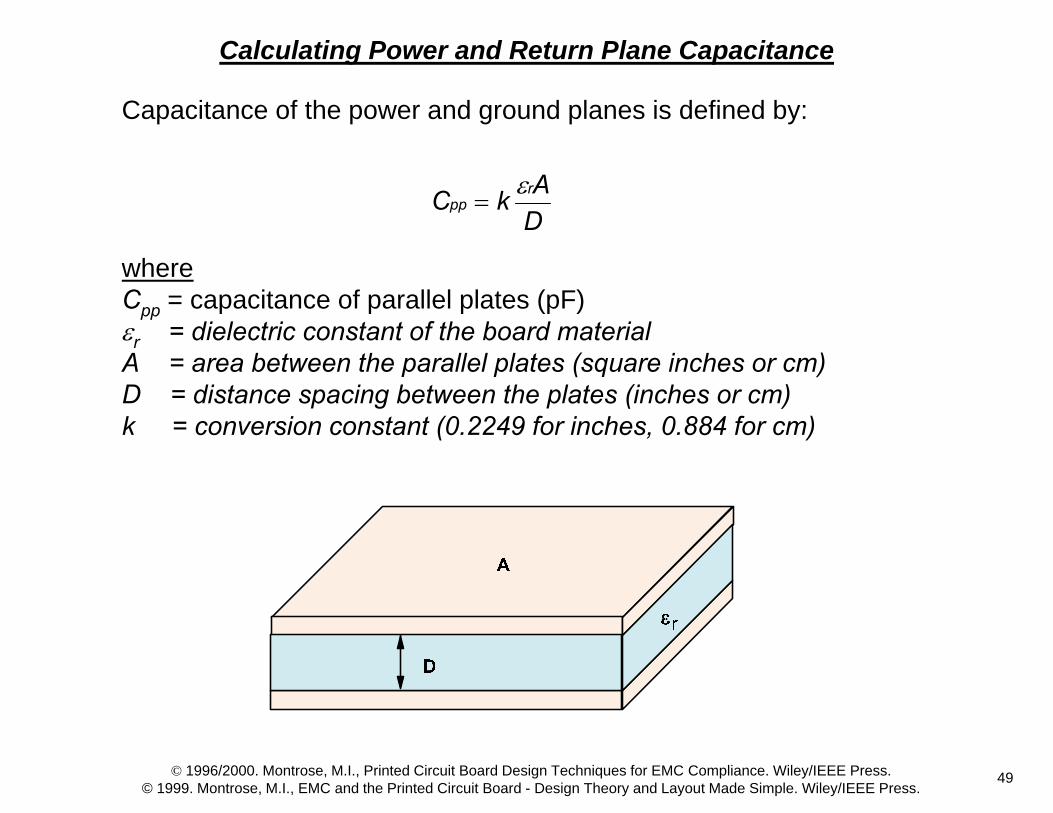
Capacitance of the power and ground planes is defined by:
whereCpp = capacitance of parallel plates (pF)r = dielectric constant of the board materialA = area between the parallel plates (square inches or cm)D = distance spacing between the plates (inches or cm)k = conversion constant (0.2249 for inches, 0.884 for cm)
DAkC r
pp
Calculating Power and Return Plane Capacitance
49

Self-resonant frequency Through-hole capacitors
0.001
0.01
0.1
1
10
100
1000
10000
1.00 10.00 100.00 1000.00
Impedance (Ohms)
Frequency (MHz)
100 pF
0.001 uF
0.01 uF
0.1 uF
Capacitors and Resonance
1/4 inch or 0.64 cm leads – 15 nH
© 1996/2000. Montrose, M.I., Printed Circuit Board Design Techniques for EMC Compliance. Wiley/IEEE Press.© 1999. Montrose, M.I., EMC and the Printed Circuit Board - Design Theory and Layout Made Simple. Wiley/IEEE Press.
50

Self Resonant Frequency - SMT Capacitors
0.001
0.01
0.1
1
10
100
1000
10000
1 10 100 1000
Impedance (Ohms)
100 pF
0.01 uF
0.1 uF
Frequency (MHz)
0.001 uF
© 1996/2000. Montrose, M.I., Printed Circuit Board Design Techniques for EMC Compliance. Wiley/IEEE Press.© 1999. Montrose, M.I., EMC and the Printed Circuit Board - Design Theory and Layout Made Simple. Wiley/IEEE Press.
51

Effects of Capacitors in Parallel – Different Values
© 1996/2000. Montrose, M.I., Printed Circuit Board Design Techniques for EMC Compliance. Wiley/IEEE Press.© 1999. Montrose, M.I., EMC and the Printed Circuit Board - Design Theory and Layout Made Simple. Wiley/IEEE Press.
52

Effects of Capacitors in Parallel – Same Capacitor Values
How to calculate number of capacitors with the same capacitive value in parallel:
(Plot provided courtesy AVX Corp.)22 1
nCnESL
nESRZ
nESRESR
nLL
CnC
total
otal
total
© 1996/2000. Montrose, M.I., Printed Circuit Board Design Techniques for EMC Compliance. Wiley/IEEE Press.© 1999. Montrose, M.I., EMC and the Printed Circuit Board - Design Theory and Layout Made Simple. Wiley/IEEE Press.
53

Power and Ground Plane Capacitance
© 1996/2000. Montrose, M.I., Printed Circuit Board Design Techniques for EMC Compliance. Wiley/IEEE Press.© 1999. Montrose, M.I., EMC and the Printed Circuit Board - Design Theory and Layout Made Simple. Wiley/IEEE Press.
54

Conflicting Rules for PCB Decoupling
List created by Todd Hubing
© 1996/2000. Montrose, M.I., Printed Circuit Board Design Techniques for EMC Compliance. Wiley/IEEE Press.© 1999. Montrose, M.I., EMC and the Printed Circuit Board - Design Theory and Layout Made Simple. Wiley/IEEE Press.
55

© 1996/2000. Montrose, M.I., Printed Circuit Board Design Techniques for EMC Compliance. Wiley/IEEE Press.© 1999. Montrose, M.I., EMC and the Printed Circuit Board - Design Theory and Layout Made Simple. Wiley/IEEE Press.
Interconnects and I/O
56

© 1996/2000. Montrose, M.I., Printed Circuit Board Design Techniques for EMC Compliance. Wiley/IEEE Press.© 1999. Montrose, M.I., EMC and the Printed Circuit Board - Design Theory and Layout Made Simple. Wiley/IEEE Press.
Partitioning
Functional SubsystemsA group of components along with their respective support circuitry performing acommon function.
Quiet AreasSections physically isolated from other functional areas to prevents noise sources from corrupting susceptible circuits in the quiet zone.
Internal Radiated Noise CouplingRadiated RF coupling may occur between different functional subsections. To prevent this coupling, a fence or shield barrier may be required. A fence is a metal barrier secured to the ground plane(s) at intervals appropriate for the highest frequencies anticipated (at /20 wavelength intervals) and tall enough in height to prevent direct line RF radiated field coupling.
57

© 1996/2000. Montrose, M.I., Printed Circuit Board Design Techniques for EMC Compliance. Wiley/IEEE Press.© 1999. Montrose, M.I., EMC and the Printed Circuit Board - Design Theory and Layout Made Simple. Wiley/IEEE Press.
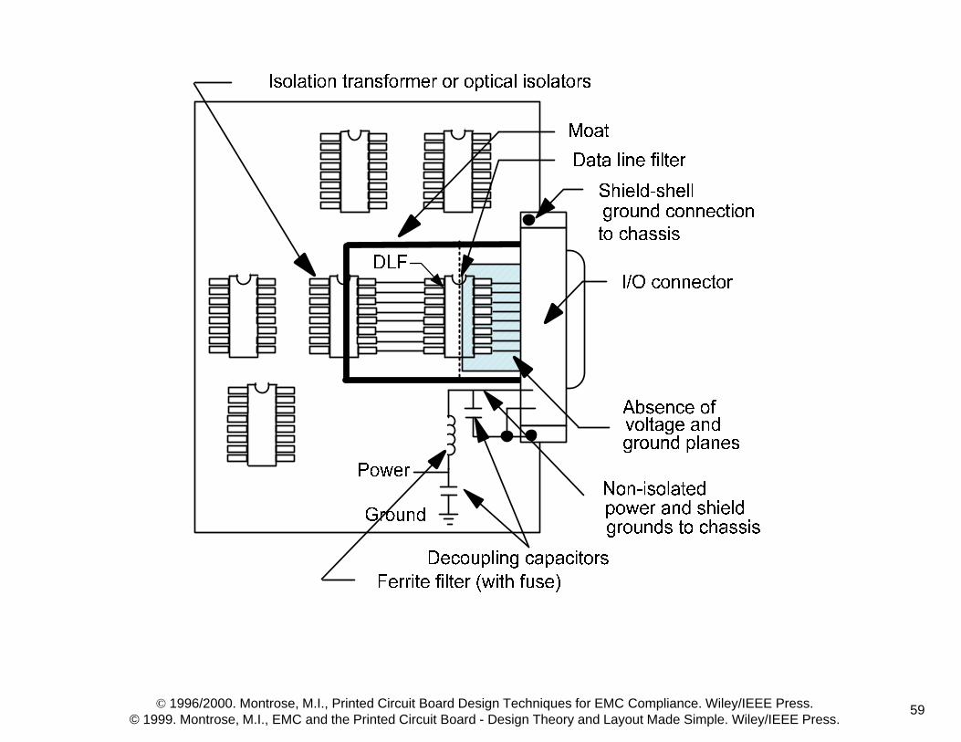
Isolation (Moating)
58
© 1996/2000. Montrose, M.I., Printed Circuit Board Design Techniques for EMC Compliance. Wiley/IEEE Press.© 1999. Montrose, M.I., EMC and the Printed Circuit Board - Design Theory and Layout Made Simple. Wiley/IEEE Press.
59

© 1996/2000. Montrose, M.I., Printed Circuit Board Design Techniques for EMC Compliance. Wiley/IEEE Press.© 1999. Montrose, M.I., EMC and the Printed Circuit Board - Design Theory and Layout Made Simple. Wiley/IEEE Press.
Bridging
I/O
MoatConnection to chassis ground
Bridge in moat
Vcc
VccVcc
Vcc
Vcc
Vcc
Ferrite bead-on-lead for optional power, if required, over a separate moat for power plane. (dotted line).
Vcc connector
Location ofoptionalgrounds tochassis
60

© 1996/2000. Montrose, M.I., Printed Circuit Board Design Techniques for EMC Compliance. Wiley/IEEE Press.© 1999. Montrose, M.I., EMC and the Printed Circuit Board - Design Theory and Layout Made Simple. Wiley/IEEE Press.
Image Plane or Moat Violation
61

© 1996/2000. Montrose, M.I., Printed Circuit Board Design Techniques for EMC Compliance. Wiley/IEEE Press.© 1999. Montrose, M.I., EMC and the Printed Circuit Board - Design Theory and Layout Made Simple. Wiley/IEEE Press.
Solution to All EMC Problems
62