Embed Size (px)
Citation preview
Introduction to optical spectroscopy
Chemistry 243
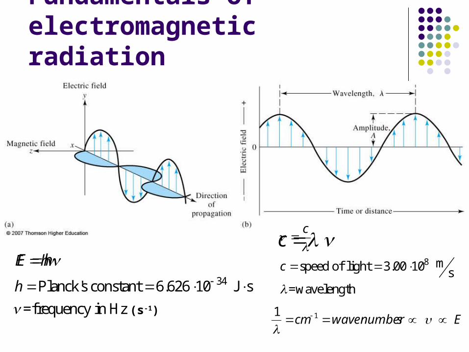
Fundamentals of electromagnetic radiation
34Planck's constant 6.626 10 J s
=frequency in Hz
E h
h
8 mspeed of light 3.00 10 s=wavelength
c
c
(s-1)Eswavenumbercm
11
hE c
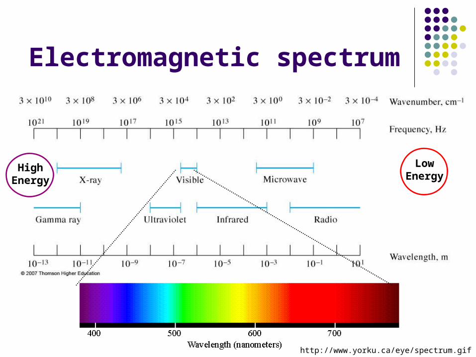
Electromagnetic spectrum
http://www.yorku.ca/eye/spectrum.gif
HighEnergy
LowEnergy
Terminology Spectroscopy is the study of the interaction of
light and matter NMR or X-Ray spectroscopy; spectroscopist
Spectrometry is the establishment of the pattern of interaction (as a function of energy) of light with particular forms of matter Mass spectrometry (MS); spectrometrist
Spectrophotometry is the quantitative study of the interaction of light with matter UV-Visible spectrophotometry (I’ve never heard anyone called a spectrophotometrist)
What chemical and/or material properties can we measure using spectral methods? Broad and powerful applications Elemental composition (often metals; CHNO) Identity of a pure substance (what is it?) Components of a mixture (purity?) Amount of a substance in a mixture (how much?) Bulk/major component, minor component,
trace component, ultra-trace component Surface composition Material property (stress/strain, polymer cross-
linking, change of state, temperature) Reaction rate, mechanism, products
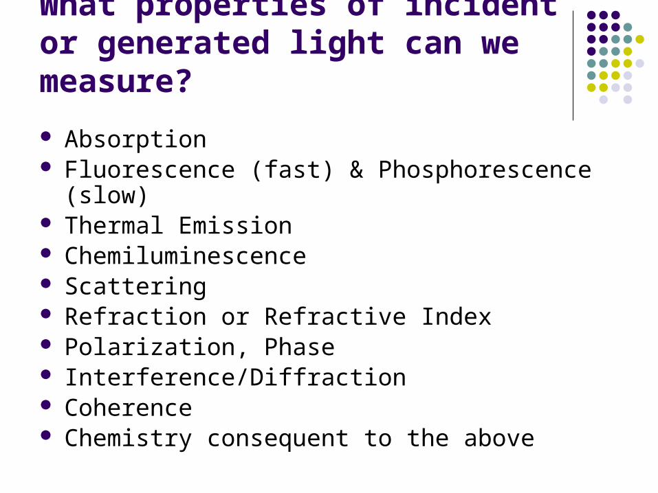
What properties of incident or generated light can we measure?
Absorption Fluorescence (fast) & Phosphorescence (slow) Thermal Emission Chemiluminescence Scattering Refraction or Refractive Index Polarization, Phase Interference/Diffraction Coherence Chemistry consequent to the above
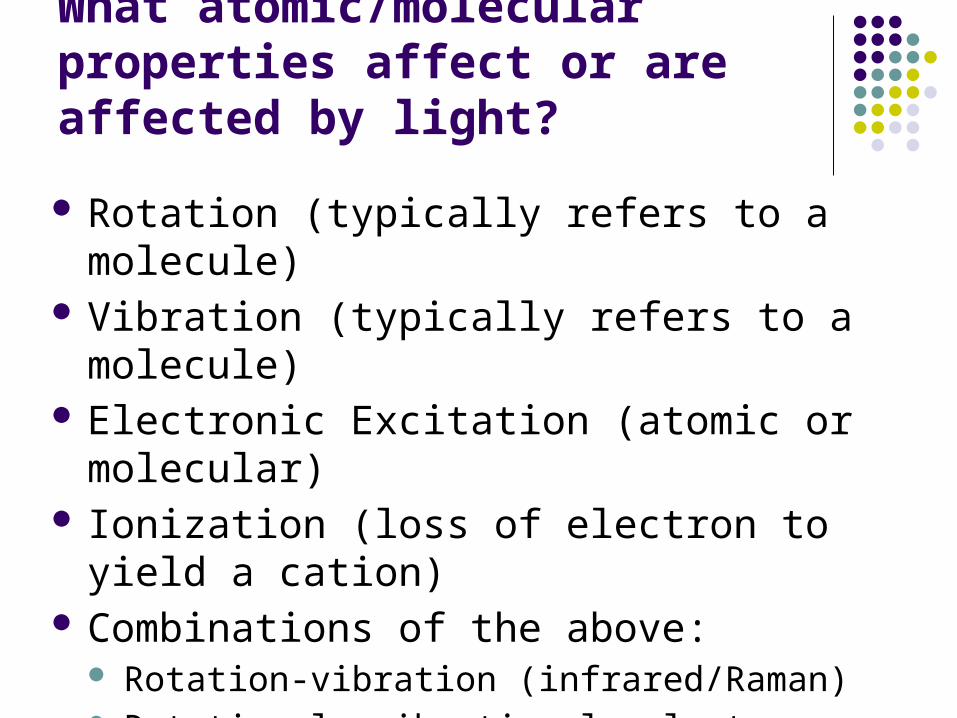
What atomic/molecular properties affect or are affected by light?
Rotation (typically refers to a molecule) Vibration (typically refers to a molecule) Electronic Excitation (atomic or molecular) Ionization (loss of electron to yield a cation) Combinations of the above:
Rotation-vibration (infrared/Raman) Rotational, vibrational, electron excitation (UV-Vis) Ionization with UV absorbance (strong excitation)
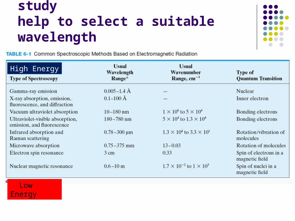
The properties you want to studyhelp to select a suitable wavelength
High Energy
Low Energy
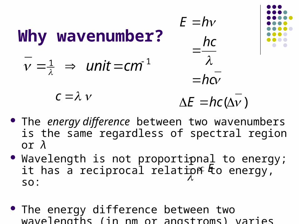
Why wavenumber?
The energy difference between two wavenumbers is the same regardless of spectral region or λ
Wavelength is not proportional to energy; it has a reciprocal relation to energy, so:
The energy difference between two wavelengths (in nm or angstroms) varies as a function of spectral region.
11 cmunit
)(
hcE
hc
hc
hE
c
E1
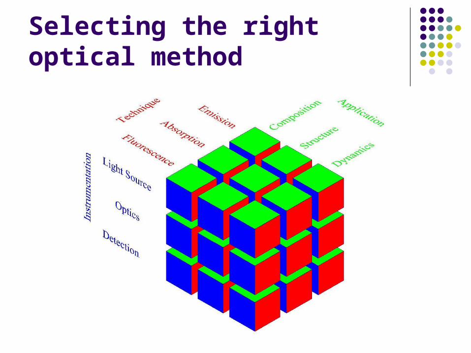
Selecting the right optical method
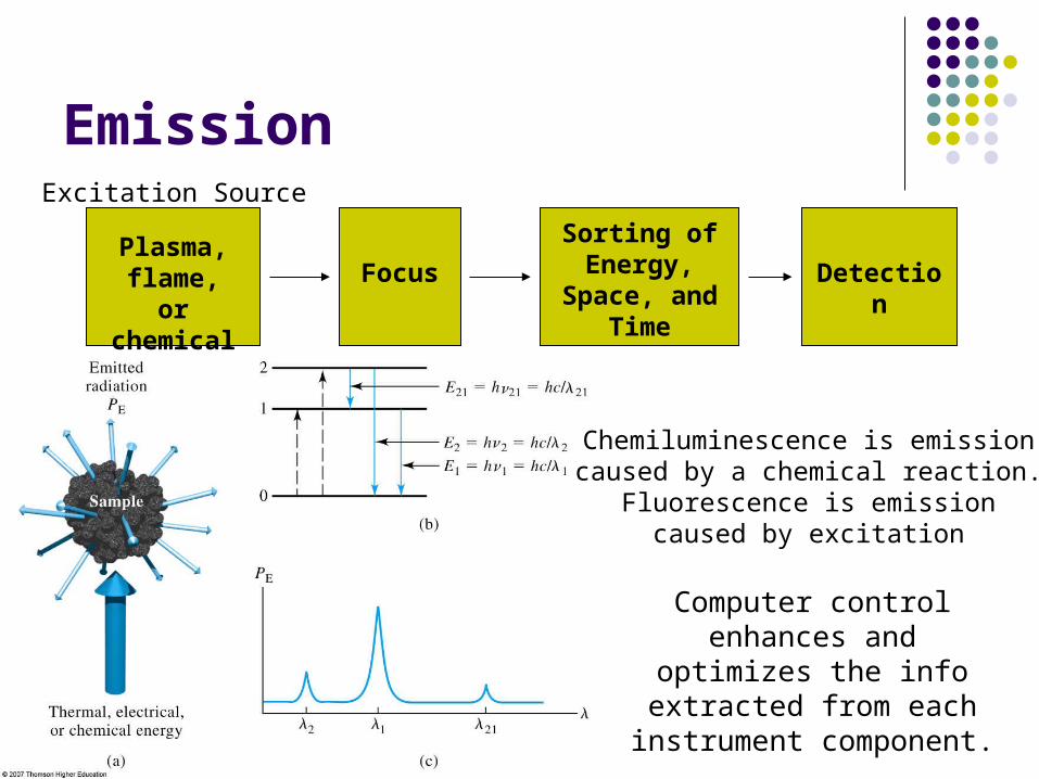
Emission
Plasma, flame, or chemical
Focus
Sorting of Energy,
Space, and Time
Detection
Computer control enhances and optimizes the info extracted from each
instrument component.
Excitation Source
Chemiluminescence is emissioncaused by a chemical reaction.
Fluorescence is emissioncaused by excitation
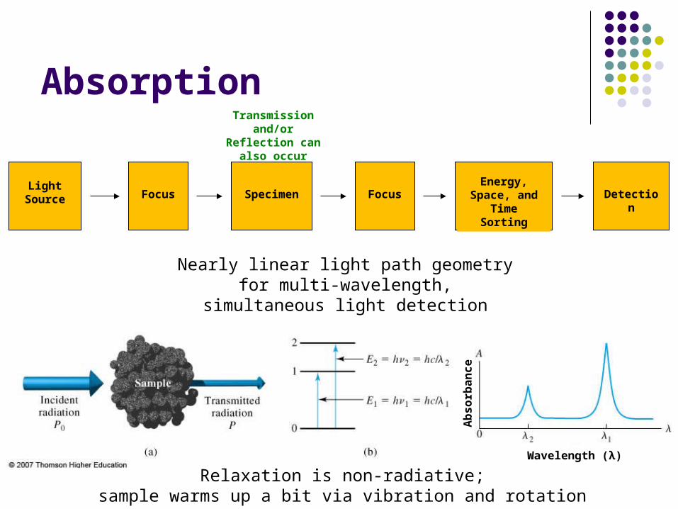
Absorption
Light Source Focus Specimen Focus
Energy, Space, and
Time SortingDetection
Transmissionand/or
Reflection canalso occur
Nearly linear light path geometryfor multi-wavelength,
simultaneous light detection
Relaxation is non-radiative;sample warms up a bit via vibration and rotation
Ab
so
rba
nc
eWavelength (λ)
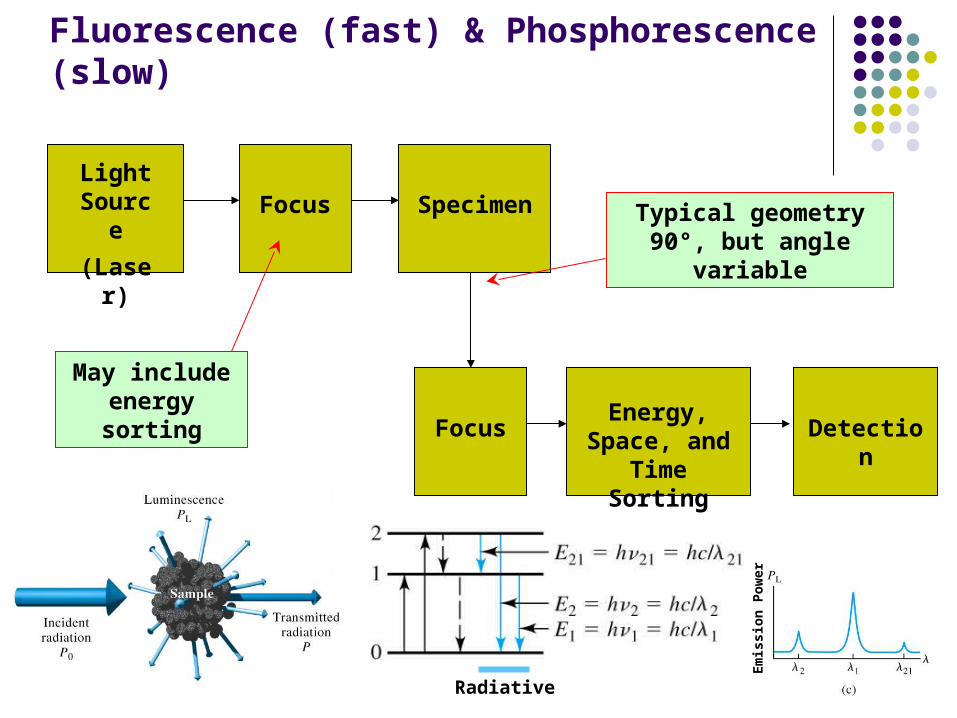
Fluorescence (fast) & Phosphorescence (slow)
Light Source
(Laser)
Focus
Focus Detection
Specimen
Energy, Space, and
Time Sorting
May include energy sorting
Typical geometry 90°, but angle variable
Em
issi
on
Po
wer
Radiative
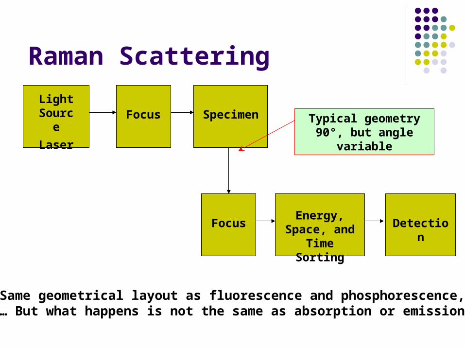
Raman Scattering
Light Source
Laser
Focus
Focus Detection
Specimen
Energy, Space, and
Time Sorting
Typical geometry 90°, but angle variable
Same geometrical layout as fluorescence and phosphorescence,… But what happens is not the same as absorption or emission
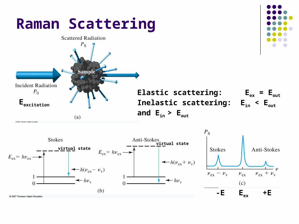
Raman Scattering
Elastic scattering: Eex = Eout
Inelastic scattering: Ein < Eout and Ein > Eout Eexcitation
Eex +E-E
virtual statevirtual state
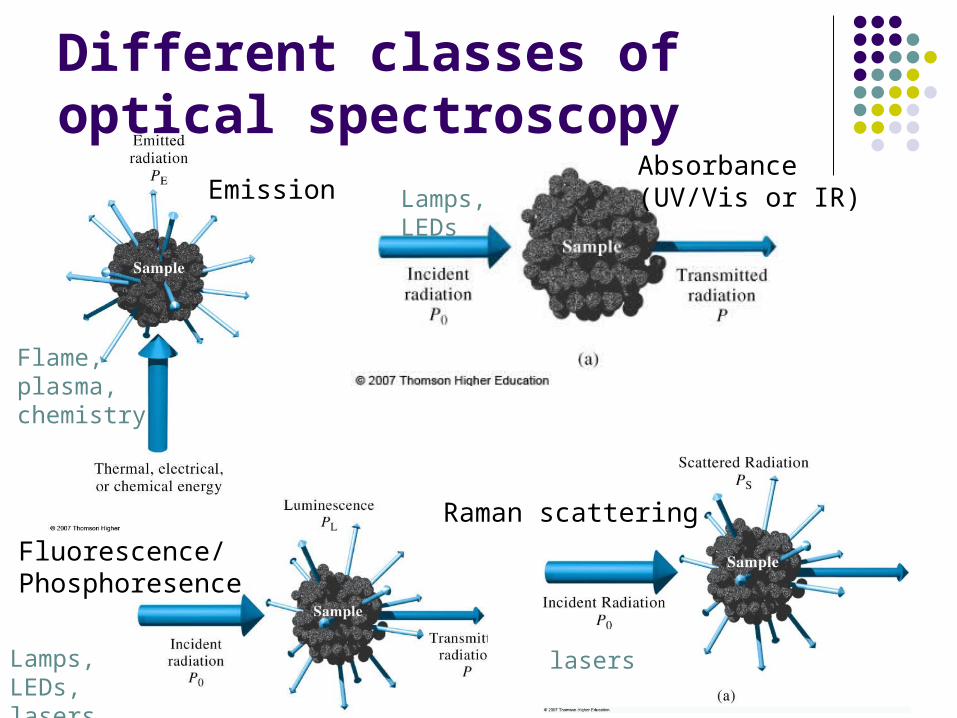
Emission
Flame, plasma, chemistry
Absorbance(UV/Vis or IR)Lamps, LEDs
Fluorescence/Phosphoresence
Lamps, LEDs, lasers
lasers
Raman scattering
Different classes of optical spectroscopy
Classes of light sources
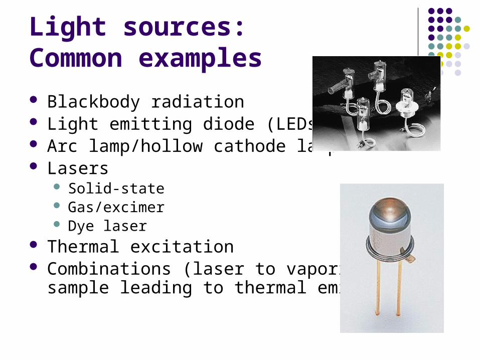
Light sources:Common examples
Blackbody radiation Light emitting diode (LEDs) Arc lamp/hollow cathode lamp Lasers
Solid-state Gas/excimer Dye laser
Thermal excitation Combinations (laser to vaporize
sample leading to thermal emission)
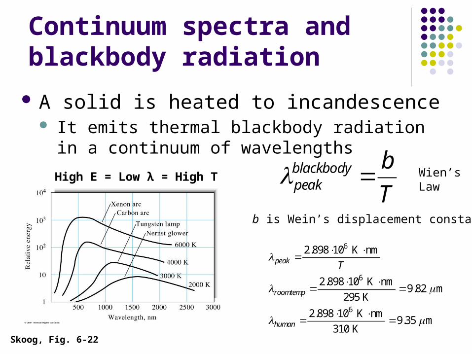
Continuum spectra and blackbody radiation
6
6
6
2.898 10 K nm
2.898 10 K nm9.82 m
295 K
2.898 10 K nm9.35 m
310 K
peak
roomtemp
human
T
A solid is heated to incandescence It emits thermal blackbody radiation in a continuum
of wavelengths
Skoog, Fig. 6-22
High E = Low λ = High T
T
bblackbodypeak Wien’s
Law
b is Wein’s displacement constant
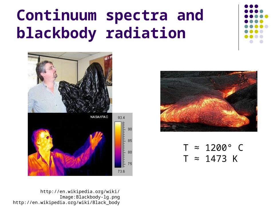
Continuum spectra and blackbody radiation
http://en.wikipedia.org/wiki/Image:Blackbody-lg.pnghttp://en.wikipedia.org/wiki/Black_body
T ≈ 1200° CT ≈ 1473 K
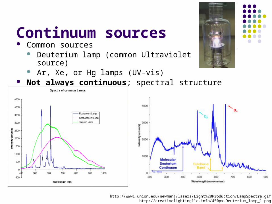
Continuum sources Common sources
Deuterium lamp (common Ultraviolet source) Ar, Xe, or Hg lamps (UV-vis)
Not always continuous; spectral structure possible
http://www1.union.edu/newmanj/lasers/Light%20Production/LampSpectra.gifhttp://creativelightingllc.info/450px-Deuterium_lamp_1.png
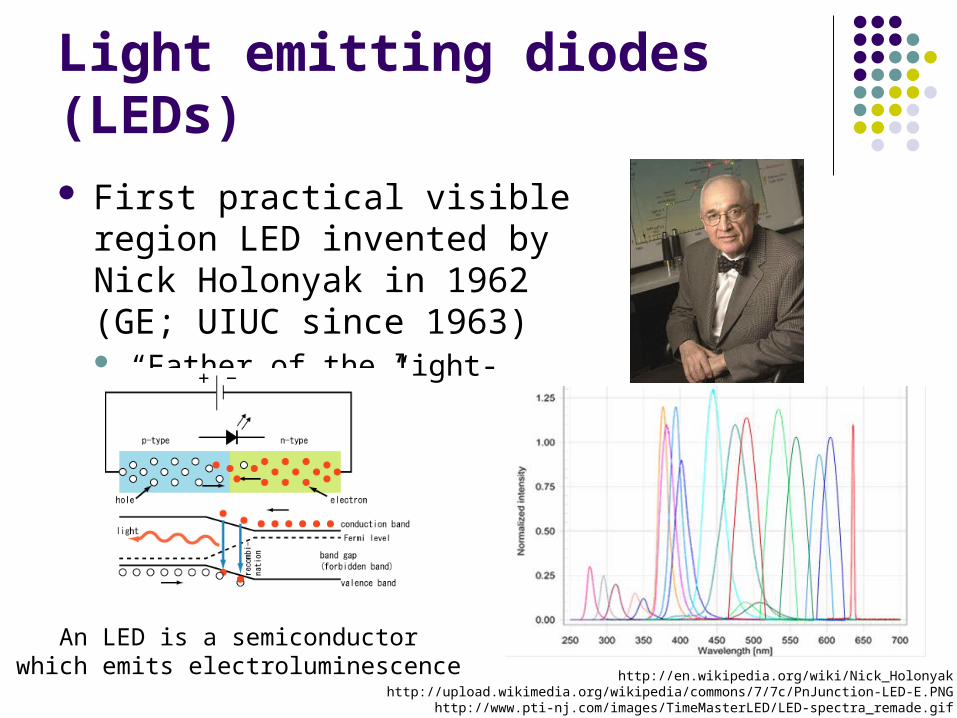
Light emitting diodes (LEDs) First practical visible region LED
invented by Nick Holonyak in 1962 (GE; UIUC since 1963) “Father of the light-emitting-diode”
http://en.wikipedia.org/wiki/Nick_Holonyakhttp://upload.wikimedia.org/wikipedia/commons/7/7c/PnJunction-LED-E.PNG
http://www.pti-nj.com/images/TimeMasterLED/LED-spectra_remade.gif
An LED is a semiconductorwhich emits electroluminescence
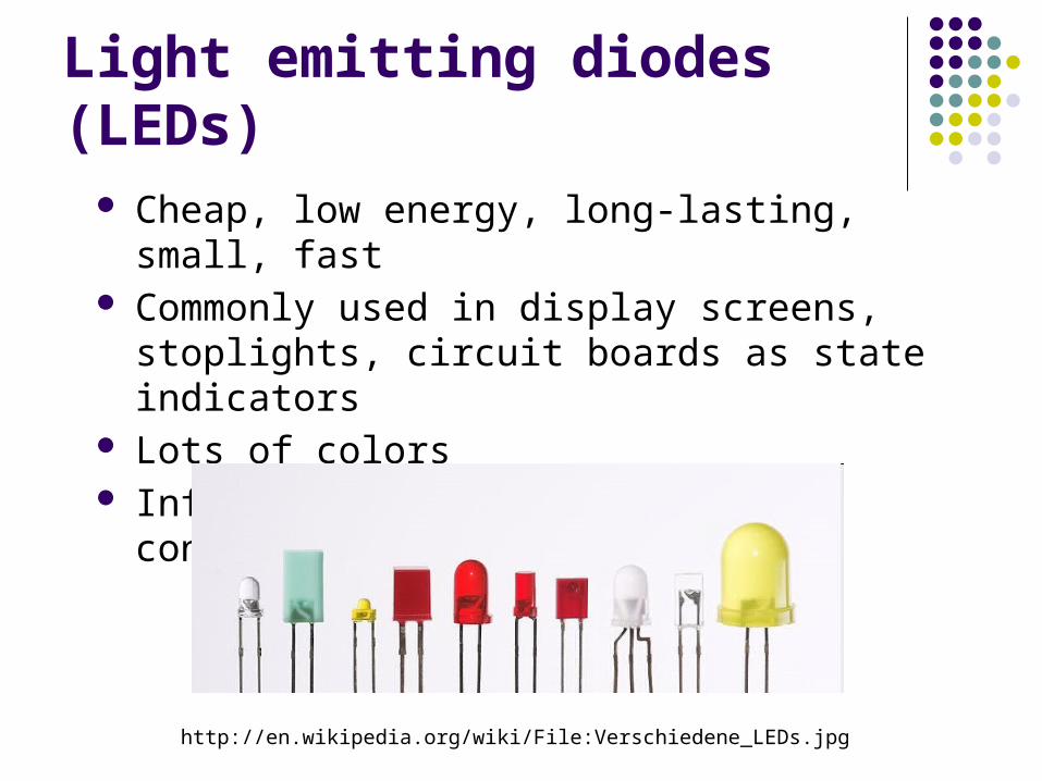
Light emitting diodes (LEDs) Cheap, low energy, long-lasting, small, fast Commonly used in display screens, stoplights,
circuit boards as state indicators Lots of colors Infrared LEDs used in remote controls
http://en.wikipedia.org/wiki/File:Verschiedene_LEDs.jpg
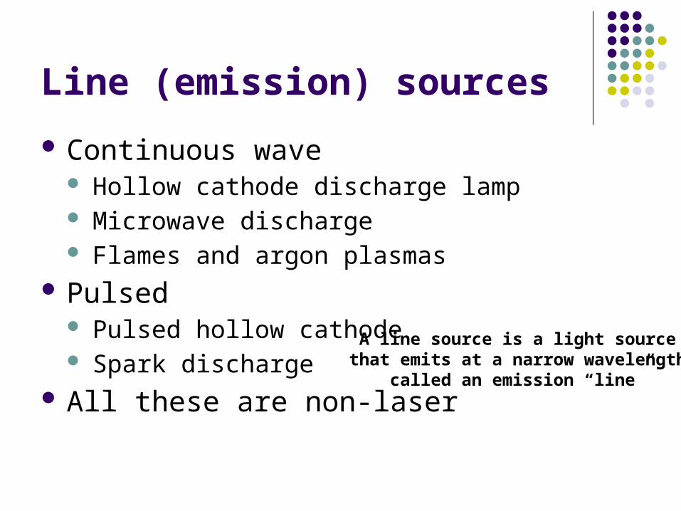
Line (emission) sources
Continuous wave Hollow cathode discharge lamp Microwave discharge Flames and argon plasmas
Pulsed Pulsed hollow cathode Spark discharge
All these are non-laser
A line source is a light sourcethat emits at a narrow wavelength
called an emission “line”
Lasers
Light Amplification byStimulated Emission
of Radiation
• Intense light source• Narrow bandwidth (small range λ < 0.01 nm)• Coherent light (in phase)
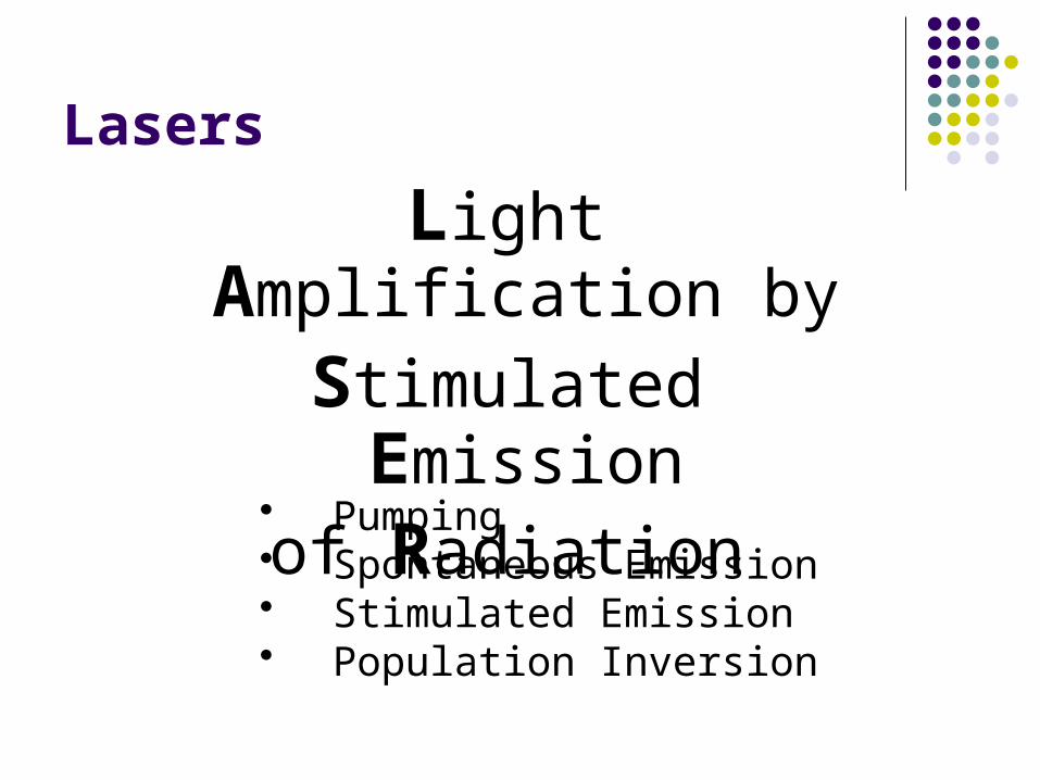
Lasers
Light Amplification byStimulated Emission
of Radiation
• Pumping• Spontaneous Emission• Stimulated Emission• Population Inversion
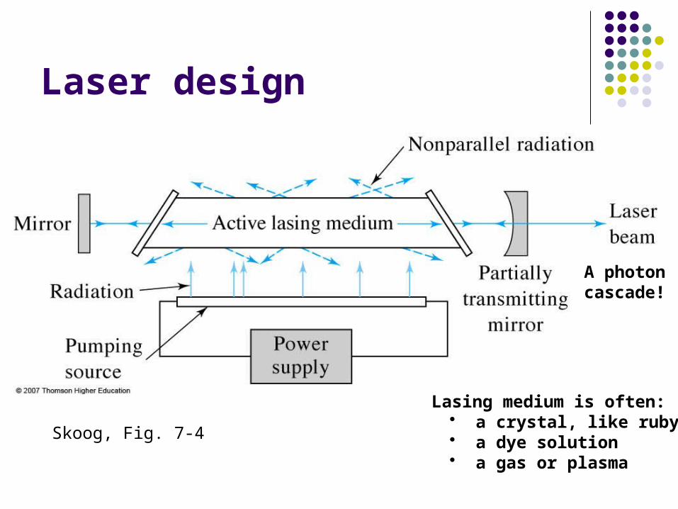
Laser design
Lasing medium is often: • a crystal, like ruby• a dye solution• a gas or plasma
A photoncascade!
Skoog, Fig. 7-4
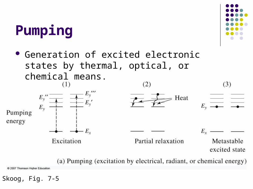
Pumping
Generation of excited electronic states by thermal, optical, or chemical means.
Skoog, Fig. 7-5
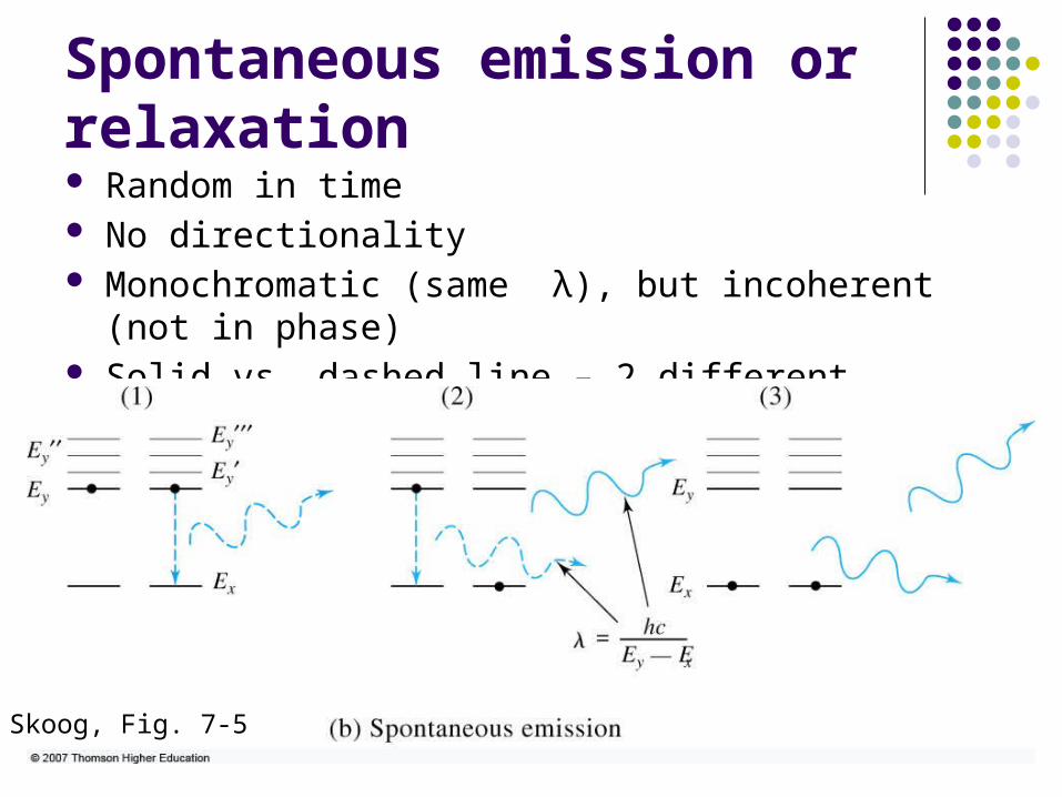
Spontaneous emission or relaxation Random in time No directionality Monochromatic (same λ), but incoherent (not in phase) Solid vs. dashed line – 2 different photons
Skoog, Fig. 7-5
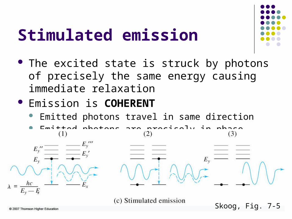
Stimulated emission
The excited state is struck by photons of precisely the same energy causing immediate relaxation
Emission is COHERENT Emitted photons travel in same direction Emitted photons are precisely in phase
Skoog, Fig. 7-5
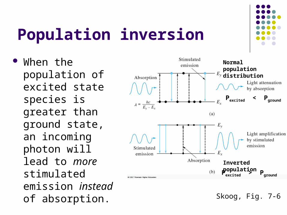
Population inversion
When the population of excited state species is greater than ground state, an incoming photon will lead to more stimulated emission instead of absorption. Inverted population
Normal population distribution
Pexcited > Pground
Pexcited < Pground
Skoog, Fig. 7-6
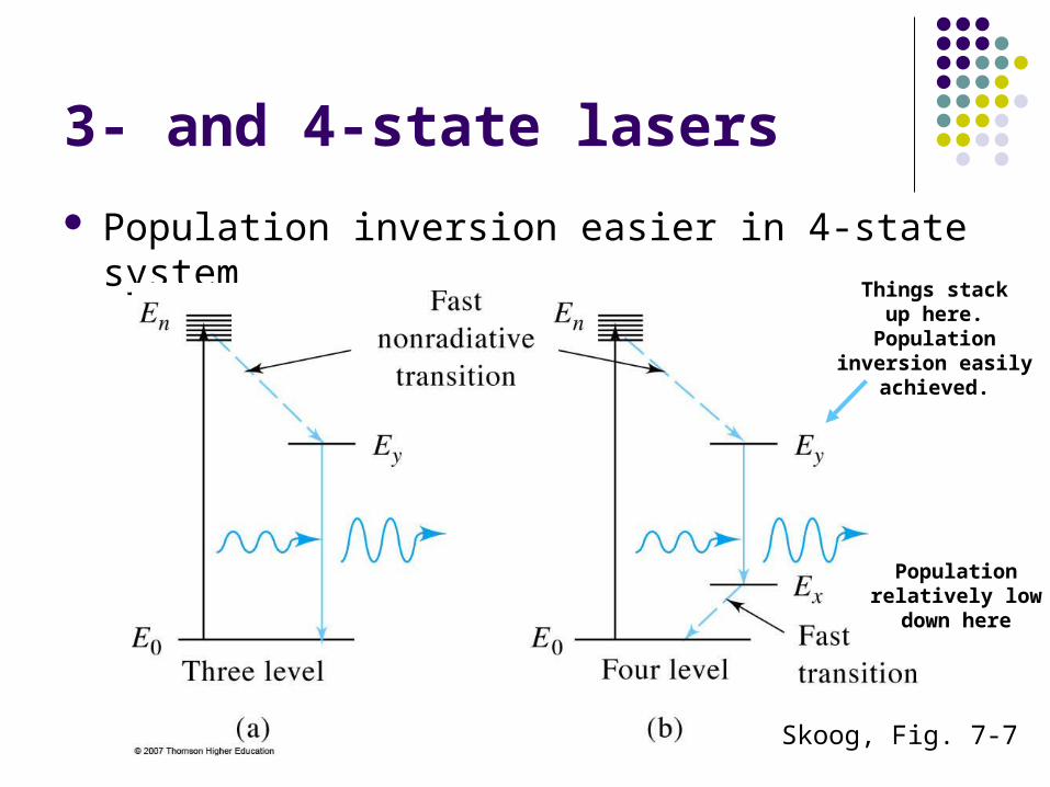
3- and 4-state lasers
Population inversion easier in 4-state system
Skoog, Fig. 7-7
Things stackup here.
Populationinversion easily
achieved.
Populationrelatively low
down here

Laser design
Lasing medium is often: • a crystal, like ruby• a dye solution• a gas or plasma
A photoncascade!
Skoog, Fig. 7-4
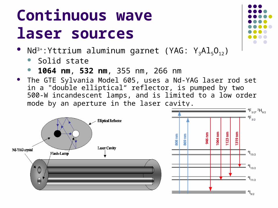
Continuous wavelaser sources Nd3+:Yttrium aluminum garnet (YAG: Y3Al5O12)
Solid state 1064 nm, 532 nm, 355 nm, 266 nm
The GTE Sylvania Model 605, uses a Nd-YAG laser rod set in a "double elliptical“ reflector, is pumped by two 500-W incandescent lamps, and is limited to a low order mode by an aperture in the laser cavity.
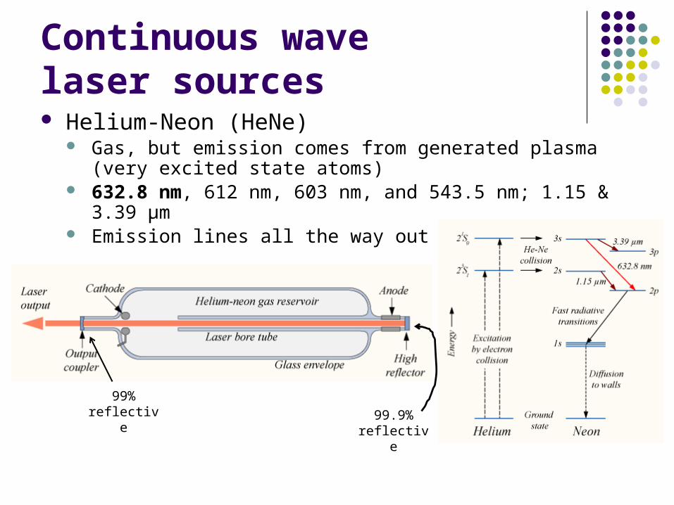
Continuous wavelaser sources Helium-Neon (HeNe)
Gas, but emission comes from generated plasma (very excited state atoms)
632.8 nm, 612 nm, 603 nm, and 543.5 nm; 1.15 & 3.39 μm Emission lines all the way out to 100 μm
99.9% reflective
99% reflective
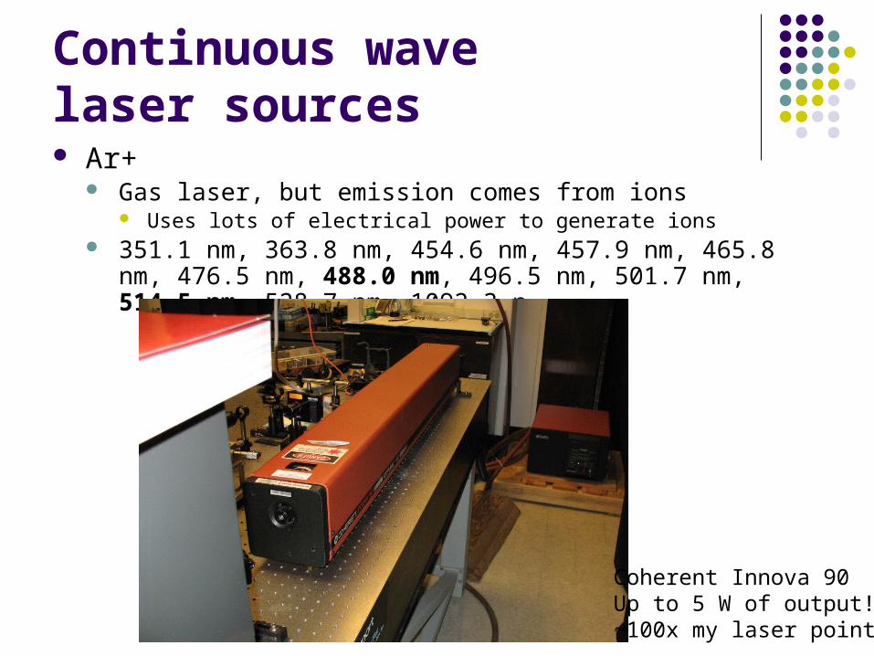
Continuous wavelaser sources Ar+
Gas laser, but emission comes from ions Uses lots of electrical power to generate ions
351.1 nm, 363.8 nm, 454.6 nm, 457.9 nm, 465.8 nm, 476.5 nm, 488.0 nm, 496.5 nm, 501.7 nm, 514.5 nm, 528.7 nm, 1092.3 n
Coherent Innova 90Up to 5 W of output!~100x my laser pointer
Other continuous wavelaser sources Cu vapor
520 nm HeCd
440 nm, 325 nm Dye lasers
Pulsed lasers sources Nd:YAG
Solid state Often nanosecond pulses 1064 nm, 532 nm, 355 nm
Ti:sapphire Solid state—often pumped by Nd:YAG Tunable output aroudn 800-1200 nm Produces femtosecond pulses
Nitrogen Gas 337 nm
Excimer lasers (gas mixtures; excited state is stable) Tunable dye lasers (λ is selective within limits)
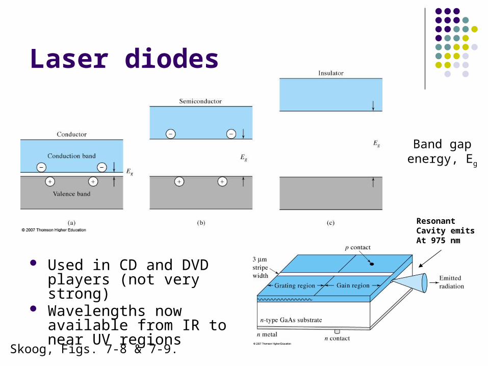
Laser diodes
Used in CD and DVD players (not very strong)
Wavelengths now available from IR to near UV regions
Band gapenergy, Eg
Skoog, Figs. 7-8 & 7-9.
ResonantCavity emitsAt 975 nm
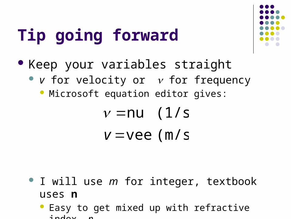
Tip going forward
Keep your variables straight v for velocity or for frequency
Microsoft equation editor gives:
I will use m for integer, textbook uses n Easy to get mixed up with refractive index, n
(m/s) vee
(1/s)nu
v
Properties of electromagnetic radiation
Transmission Refraction Reflection Scattering Optical Components Interference Diffraction
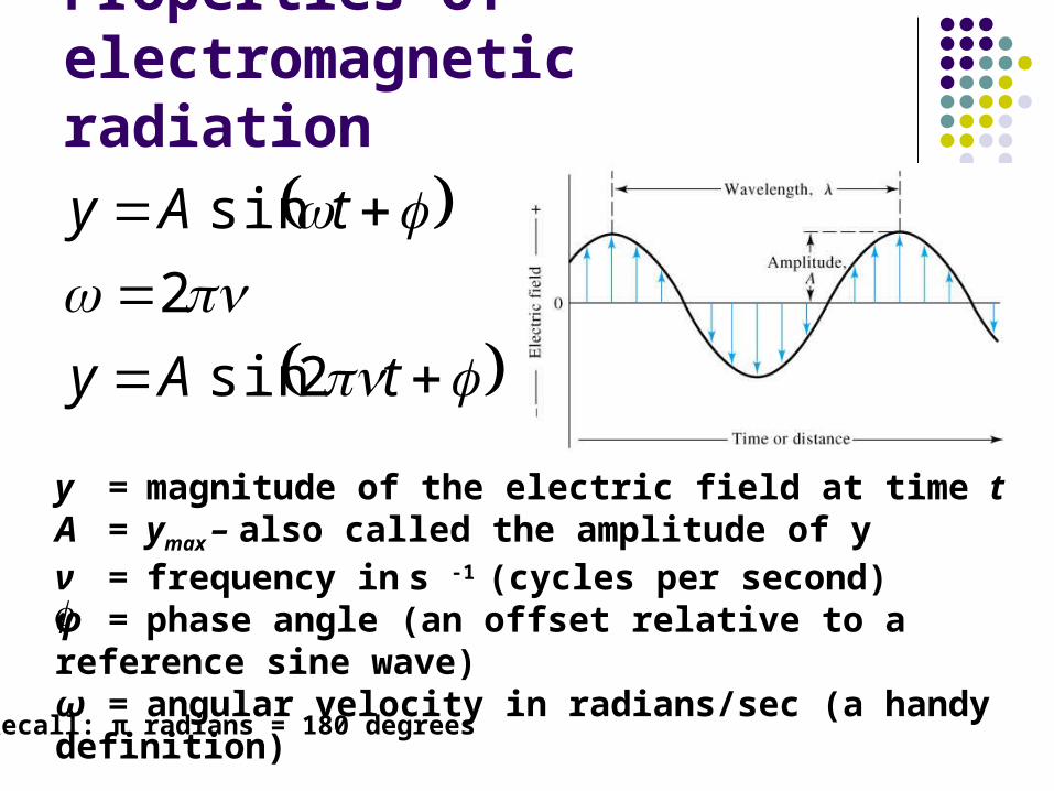
Properties of electromagnetic radiation
tAy
tAy
2sin
2
sin
y = magnitude of the electric field at time tA = ymax – also called the amplitude of yν = frequency in s -1 (cycles per second)φ = phase angle (an offset relative to a reference sine wave)ω = angular velocity in radians/sec (a handy definition)
Recall: π radians = 180 degrees
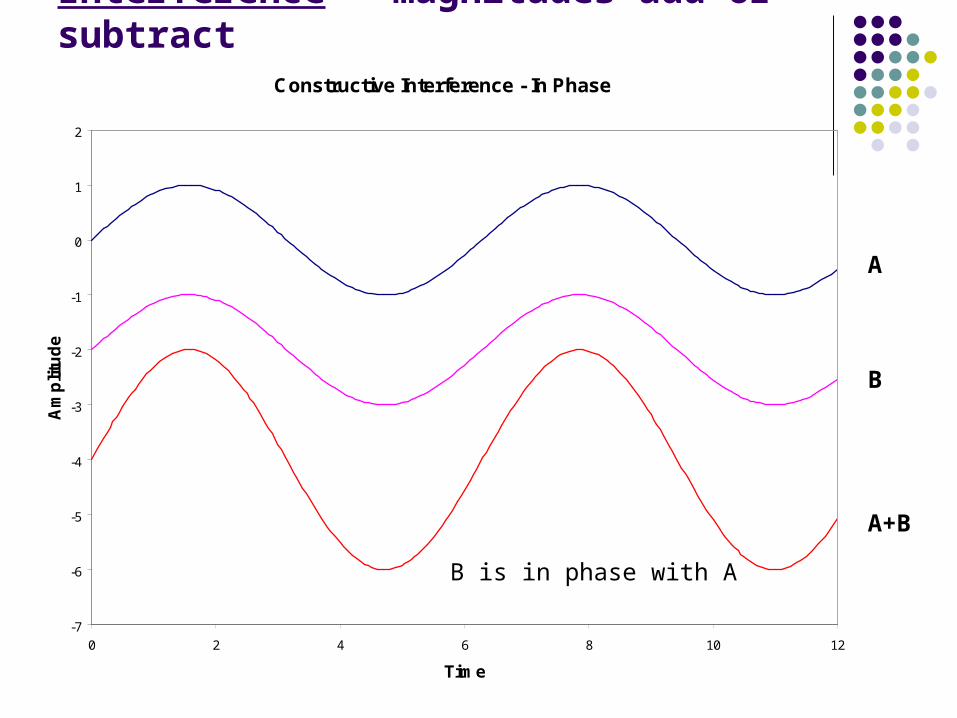
Constructive Interference - In Phase
-7
-6
-5
-4
-3
-2
-1
0
1
2
0 2 4 6 8 10 12
Time
Am
plit
ud
e
A
B
A+B
B is in phase with A
Interference – magnitudes add or subtract
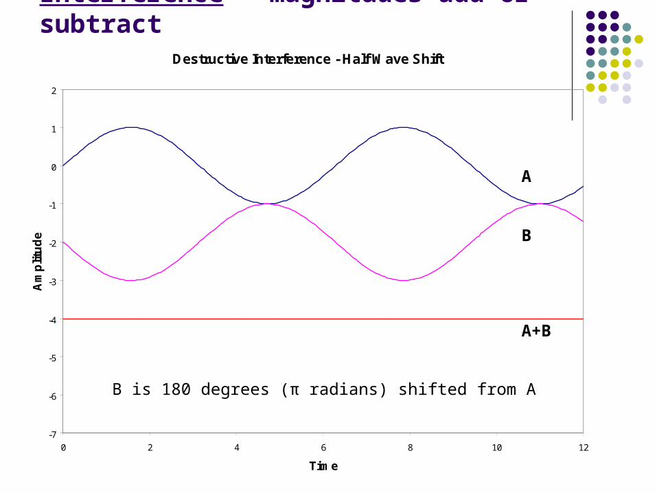
Destructive Interference - Half Wave Shift
-7
-6
-5
-4
-3
-2
-1
0
1
2
0 2 4 6 8 10 12
Time
Am
plit
ud
e
A
B
A+B
B is 180 degrees (π radians) shifted from A
Interference – magnitudes add or subtract
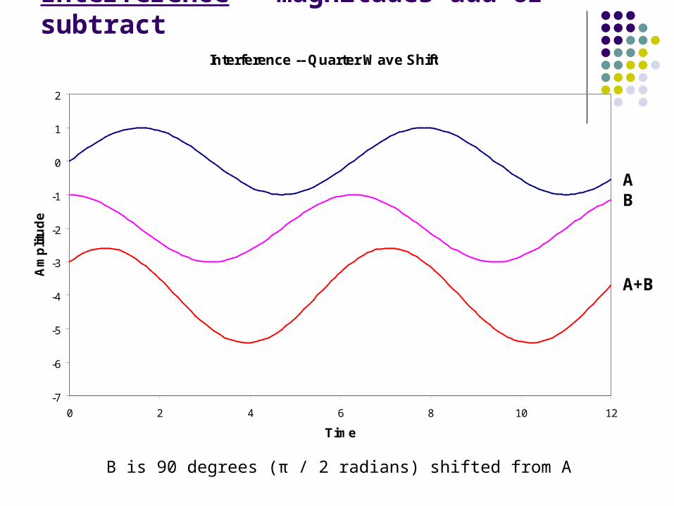
Interference -- Quarter Wave Shift
-7
-6
-5
-4
-3
-2
-1
0
1
2
0 2 4 6 8 10 12
Time
Am
plit
ud
e
AB
A+B
B is 90 degrees (π / 2 radians) shifted from A
Interference – magnitudes add or subtract
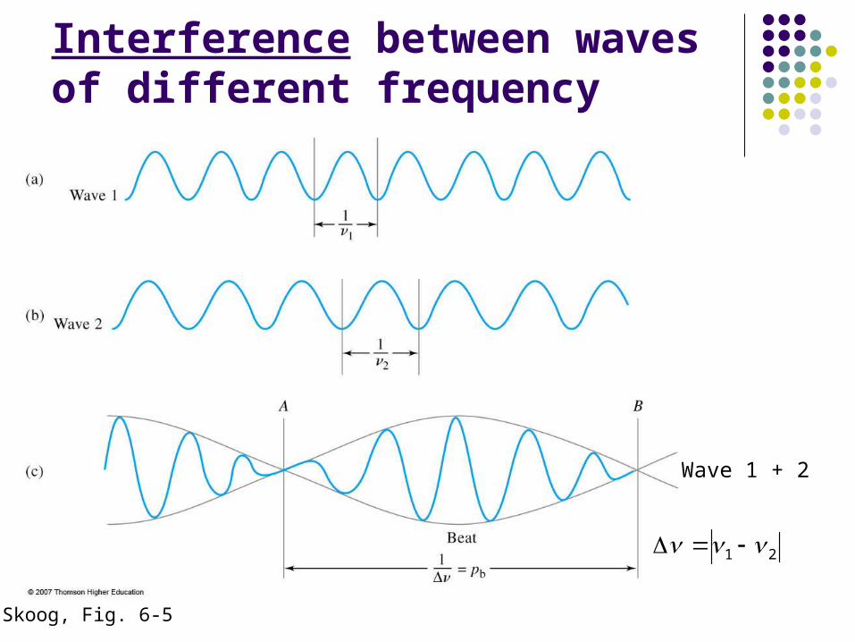
Interference between waves of different frequency
Wave 1 + 2
21
Skoog, Fig. 6-5
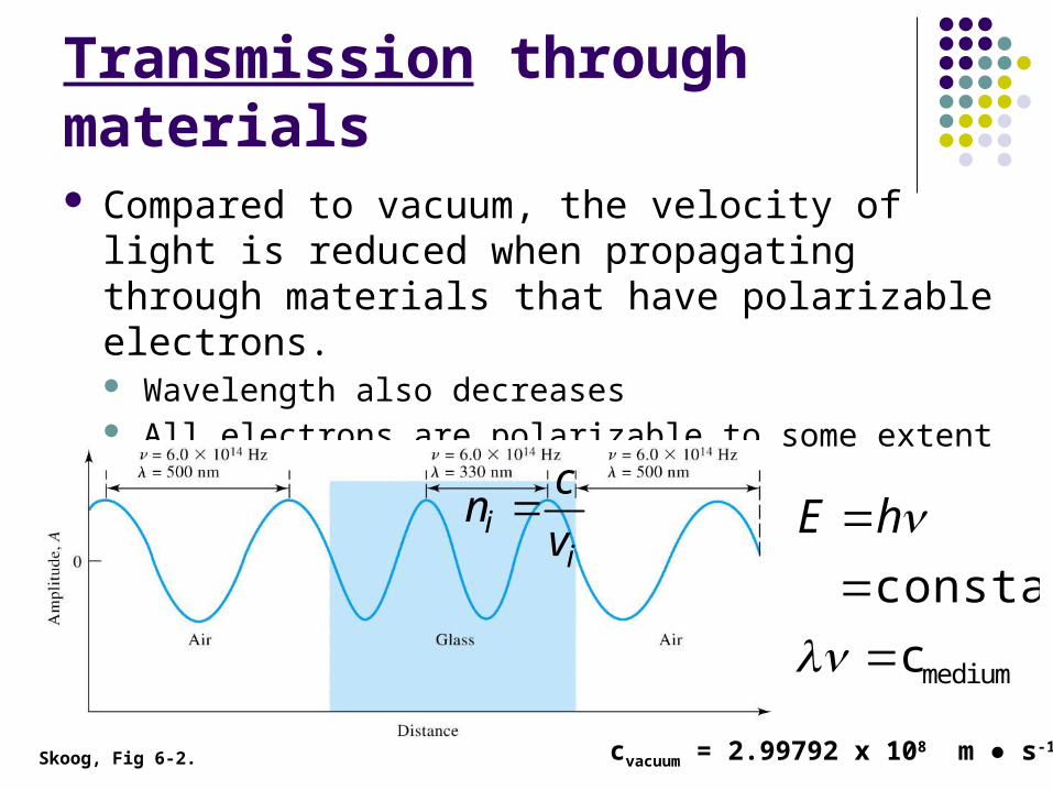
Transmission through materials Compared to vacuum, the velocity of light is reduced
when propagating through materials that have polarizable electrons. Wavelength also decreases All electrons are polarizable to some extent
ii
cn
v
Skoog, Fig 6-2.
mediumc
constant
hE
cvacuum = 2.99792 x 10⁸ m ● s-1
Index of Refraction
Refractive index is measure of how much light is slowed:
Refractive index is wavelength- and temperature-dependent for many materials:
1.46Quartz
1.49Toluene
1.43Hexadecane
1.58Glass(light flint)
1.33Water
1.00Vacuum (air)
n @ 589.3 nmMaterial Wavelength-dependence of nSiO2
http://www.rp-photonics.com/refractive_index.html
nwater vs Temperature
1.316
1.318
1.32
1.322
1.324
1.326
1.328
1.33
1.332
1.334
1.336
0 20 40 60 80 100
temperature (oC)
refr
ac
tiv
e in
de
x
lengthgiven wave aat velocity
1)(lengthgiven wave aat index refractive
i
i
vacuumi
v
v
cn
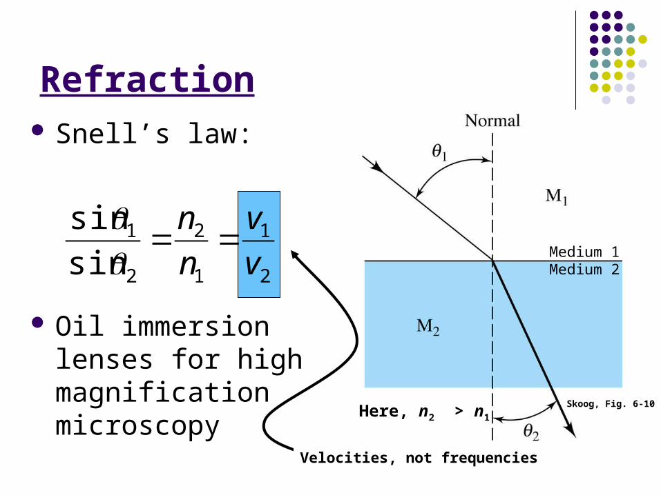
Refraction Snell’s law:
Oil immersion lenses for high magnification microscopy
2
1
1
2
2
1
sin
sin
v
v
n
n
Velocities, not frequencies
Medium 1Medium 2
Here, n2 > n1
Skoog, Fig. 6-10
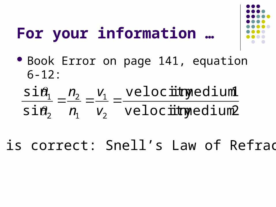
For your information …
Book Error on page 141, equation 6-12:
2 medium invelocity
1 medium invelocity
sin
sin
2
1
1
2
2
1 v
v
n
n
This is correct: Snell’s Law of Refraction
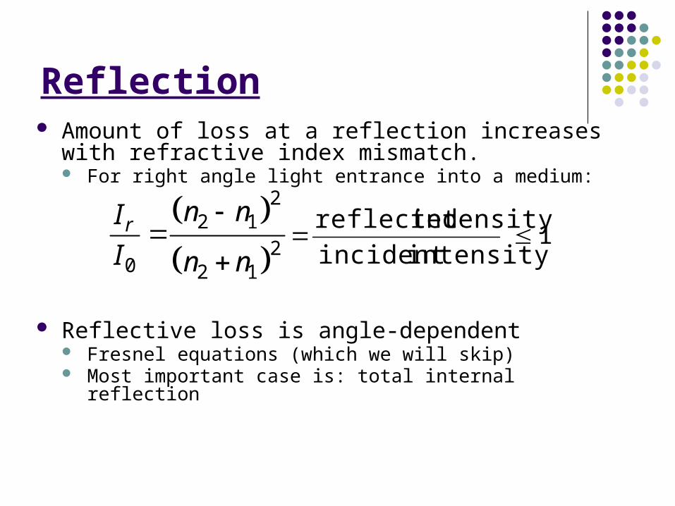
Reflection Amount of loss at a reflection increases with refractive
index mismatch. For right angle light entrance into a medium:
Reflective loss is angle-dependent Fresnel equations (which we will skip) Most important case is: total internal reflection
22 1
20 2 1
r n nI
I n n
1
intensityincident
intensity reflected
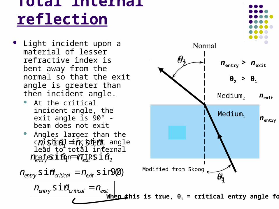
Total internal reflection Light incident upon a material
of lesser refractive index is bent away from the normal so that the exit angle is greater than then incident angle. At the critical incident angle,
the exit angle is 90° - beam does not exit
Angles larger than the critical incident angle lead to total internal refection (TIR)
exitcriticalentry
exitcriticalentry
exitentry
nn
nn
nn
nn
sin
)90sin(sin
sinsin
sinsin
21
2211
Medium1
Medium2
nentry
nexit
1
2
Modified from Skoog
nentry > nexit
θ2 > θ1
When this is true, θ1 = critical entry angle for TIR
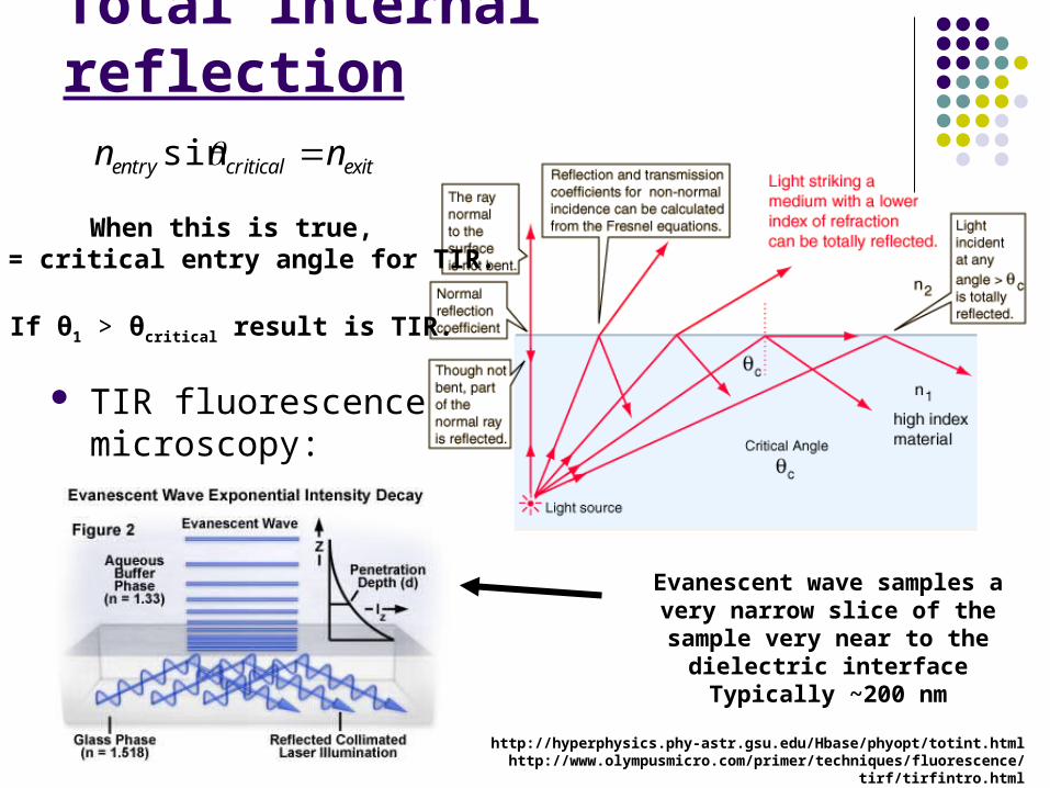
Total internal reflection
TIR fluorescence microscopy:
http://hyperphysics.phy-astr.gsu.edu/Hbase/phyopt/totint.htmlhttp://www.olympusmicro.com/primer/techniques/fluorescence/tirf/tirfintro.html
exitcriticalentry nn sin
When this is true,θ1 = critical entry angle for TIR.
If θ1 > θcritical result is TIR.
Evanescent wave samples a very narrow slice of the sample very near
to the dielectric interfaceTypically ~200 nm
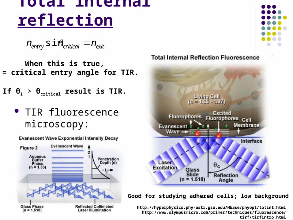
Total internal reflection
TIR fluorescence microscopy:
exitcriticalentry nn sin
When this is true,θ1 = critical entry angle for TIR.
If θ1 > θcritical result is TIR.
http://hyperphysics.phy-astr.gsu.edu/Hbase/phyopt/totint.htmlhttp://www.olympusmicro.com/primer/techniques/fluorescence/tirf/tirfintro.html
Good for studying adhered cells; low background
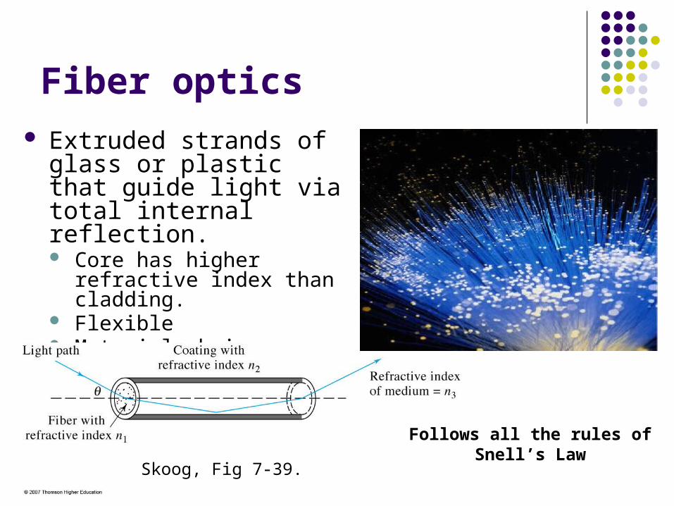
Fiber optics Extruded strands of glass
or plastic that guide light via total internal reflection. Core has higher refractive
index than cladding. Flexible Material choice allows
transmission in UV, visible, or IR
Skoog, Fig 7-39.
Follows all the rules ofSnell’s Law
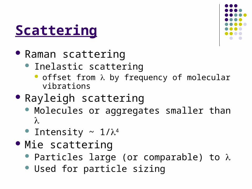
Scattering
Raman scattering Inelastic scattering
offset from by frequency of molecular vibrations Rayleigh scattering
Molecules or aggregates smaller than l Intensity ~ 1/l4
Mie scattering Particles large (or comparable) to l Used for particle sizing
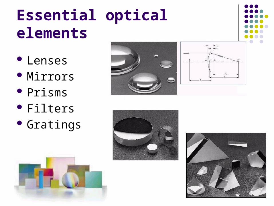
Essential optical elements
Lenses Mirrors Prisms Filters Gratings
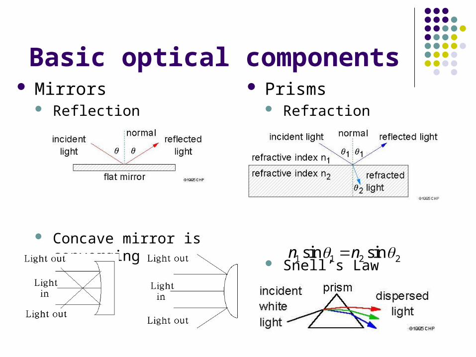
Basic optical components Mirrors
Reflection
Concave mirror is converging
Convex mirror is diverging
Prisms Refraction
Snell’s Law
1 1 2 2sin sinn n
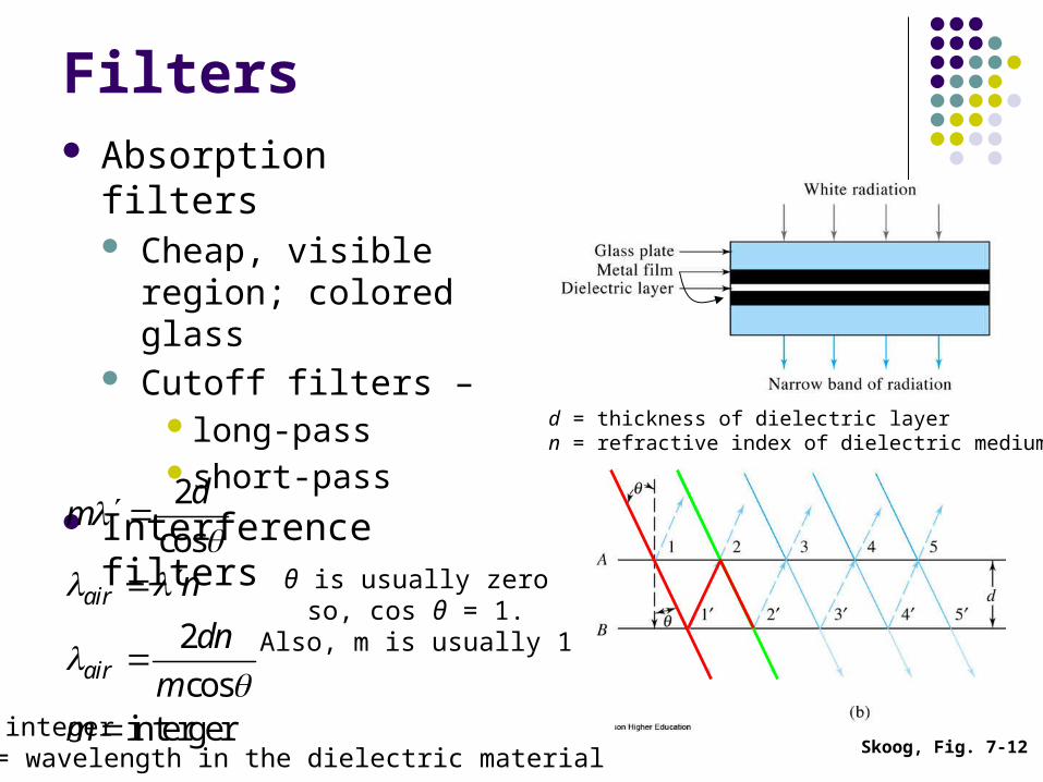
Filters Absorption filters
Cheap, visible region; colored glass
Cutoff filters – long-passshort-pass
Interference filters2
cos
2
cosinterger
air
air
dm
n
dn
mm
Skoog, Fig. 7-12
θ is usually zeroso, cos θ = 1.
Also, m is usually 1
d = thickness of dielectric layern = refractive index of dielectric medium
m = integerʹ = wavelength in the dielectric material
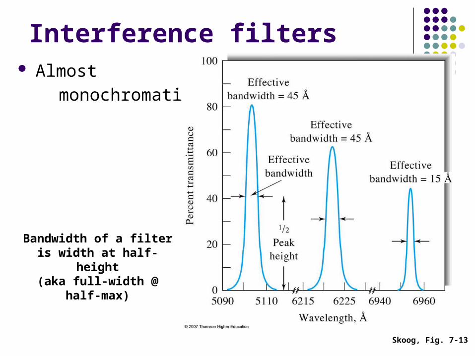
Interference filters Almost
monochromatic
Skoog, Fig. 7-13
Bandwidth of a filter is width at half-height
(aka full-width @ half-max)
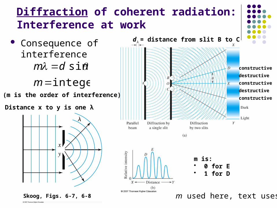
Diffraction of coherent radiation: Interference at work
Consequence of interference
Skoog, Figs. 6-7, 6-8
integer
sin
m
dm constructive
destructive
constructive
constructive
destructive
d = distance from slit B to C
Distance x to y is one λ
(m is the order of interference)
m is: • 0 for E• 1 for D
m used here, text uses n
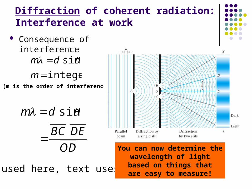
Diffraction of coherent radiation: Interference at work
Consequence of interference
integer
sin
m
dm
(m is the order of interference)
OD
DEBC
dm
sin
m used here, text uses n
You can now determine thewavelength of light
based on things thatare easy to measure!
Skoog, Fig. 6-8
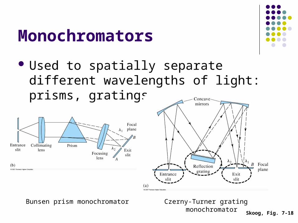
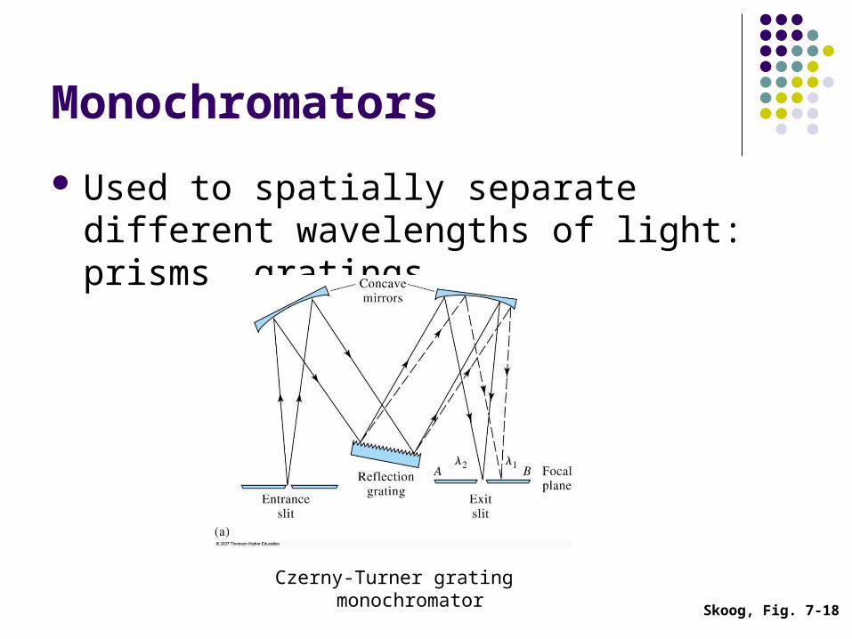
Monochromators
Used to spatially separate different wavelengths of light: prisms, gratings
Czerny-Turner grating monochromatorBunsen prism monochromator
Skoog, Fig. 7-18
Gratings and monochromatorsReflection + diffraction: echellette-type grating
sin
sin
sin sin
m CB BD
CB d i
BD d r
m d i r
Skoog, Fig. 7-21
The condition forconstructive interference.
The m = 1 line is most intense.
The surface contains “grooves” or “blazes”.
Take a look atExample 7-1,
Page 184.
Monochromators
Used to spatially separate different wavelengths of light: prisms, gratings
Czerny-Turner grating monochromator
Skoog, Fig. 7-18
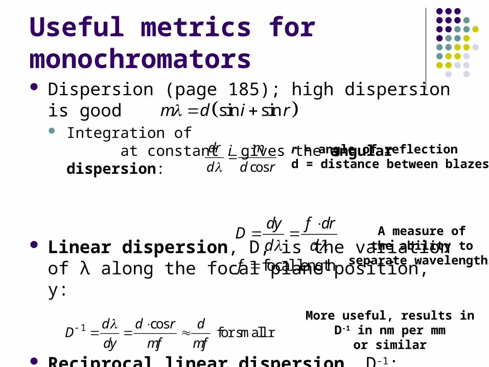
Useful metrics for monochromators Dispersion (page 185); high dispersion is good
Integration of at constant i gives the angular dispersion:
Linear dispersion, D, is the variation of λ along the focal plane position, y:
Reciprocal linear dispersion, D-1:
sin sinm d i r
cos
dr m
d d r
focal length
dy f drD
d df
1 cos for small r
d d r dD
dy mf mf
r = angle of reflectiond = distance between blazes
More useful, results inD-1 in nm per mm
or similar
A measure ofthe ability to
separate wavelengths
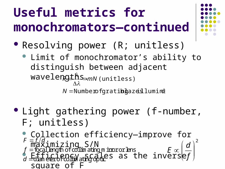
Useful metrics for monochromators—continued Resolving power (R; unitless)
Limit of monochromator’s ability to distinguish between adjacent wavelengths.
Light gathering power (f-number, F; unitless) Collection efficiency—improve for maximizing S/N Efficiency scales as the inverse square of F
focal length of collimating mirror or lens
diameter of collimating optic
F f d
f
d
dilluminate blazes grating ofNumber
(unitless)
N
mNR
2
f
dE
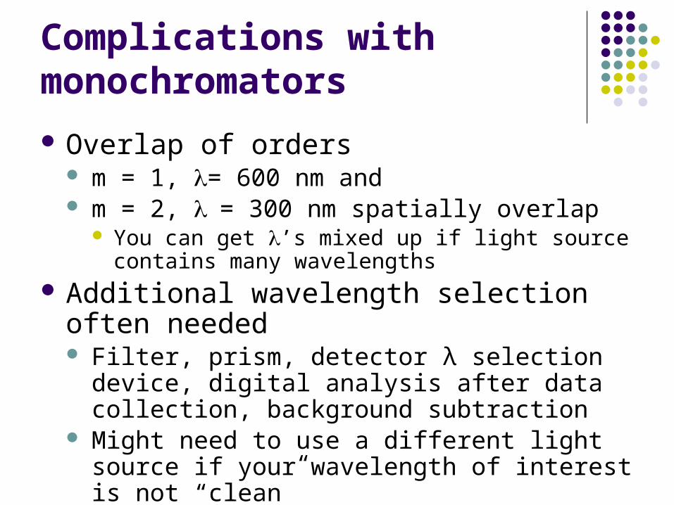
Complications with monochromators
Overlap of orders m = 1, l= 600 nm and m = 2, l = 300 nm spatially overlap
You can get ’s mixed up if light source contains many wavelengths
Additional wavelength selection often needed Filter, prism, detector λ selection device, digital
analysis after data collection, background subtraction
Might need to use a different light source if your wavelength of interest is not “clean”
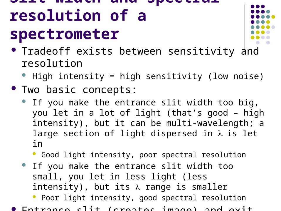
Slit width and spectral resolution of a spectrometer Tradeoff exists between sensitivity and resolution
High intensity = high sensitivity (low noise) Two basic concepts:
If you make the entrance slit width too big, you let in a lot of light (that’s good – high intensity), but it can be multi-wavelength; a large section of light dispersed in l is let in Good light intensity, poor spectral resolution
If you make the entrance slit width too small, you let in less light (less intensity), but its l range is smaller Poor light intensity, good spectral resolution
Entrance slit (creates image) and exit slit (output filter) Usually the same width
Optimal slit width based upon grating dispersion
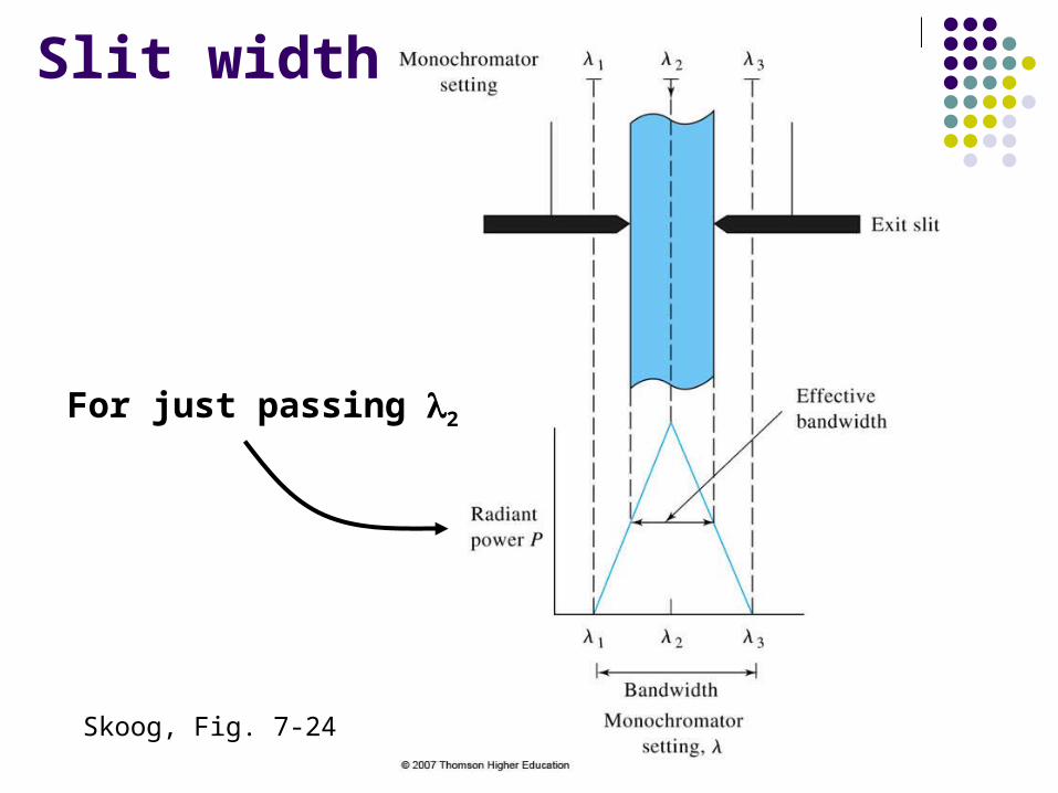
Slit width
Skoog, Fig. 7-24
For just passing l2
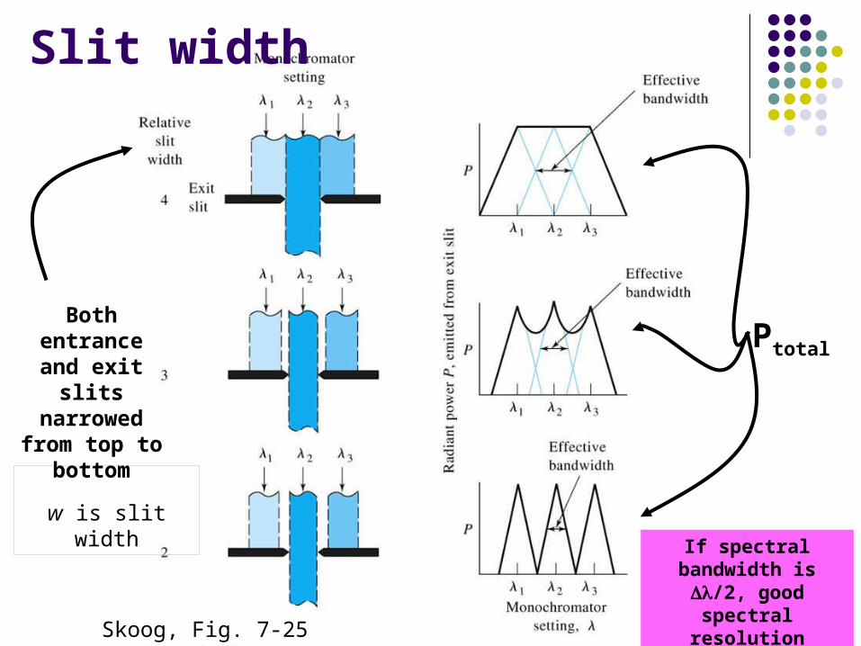
Skoog, Fig. 7-25
Ptotal
If spectral bandwidth is Dl/2, good spectral
resolution
Both entrance and exit slits
narrowed from top to bottom
Slit width
w is slit width
Skoog, Fig. 7-26
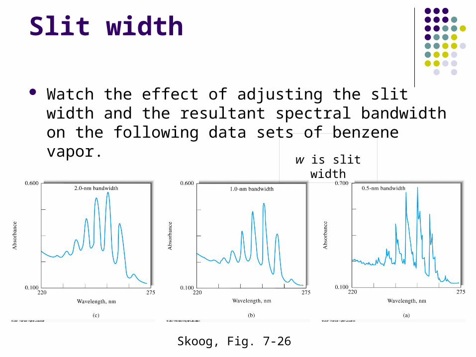
Slit width
Watch the effect of adjusting the slit width and the resultant spectral bandwidth on the following data sets of benzene vapor.
w is slit width
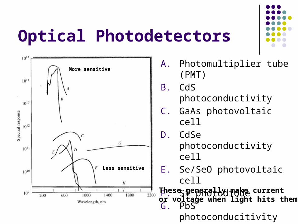
Optical Photodetectors
A. Photomultiplier tube (PMT)
B. CdS photoconductivity
C. GaAs photovoltaic cell
D. CdSe photoconductivity cell
E. Se/SeO photovoltaic cell
F. Si photodiode
G. PbS photoconducitivity
H. Thermocouple
I. Golay cell
These generally make currentor voltage when light hits them.
More sensitive
Less sensitive
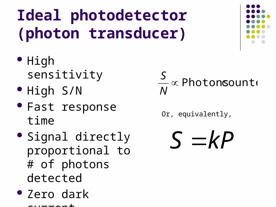
Ideal photodetector(photon transducer)
High sensitivity High S/N Fast response time Signal directly
proportional to # of photons detected
Zero dark current The blank is zero
counted PhotonsN
S
kPS Or, equivalently,
High sensitivity High S/N Fast response time Signal directly
proportional to # of photons detected
Zero dark current The blank is zero
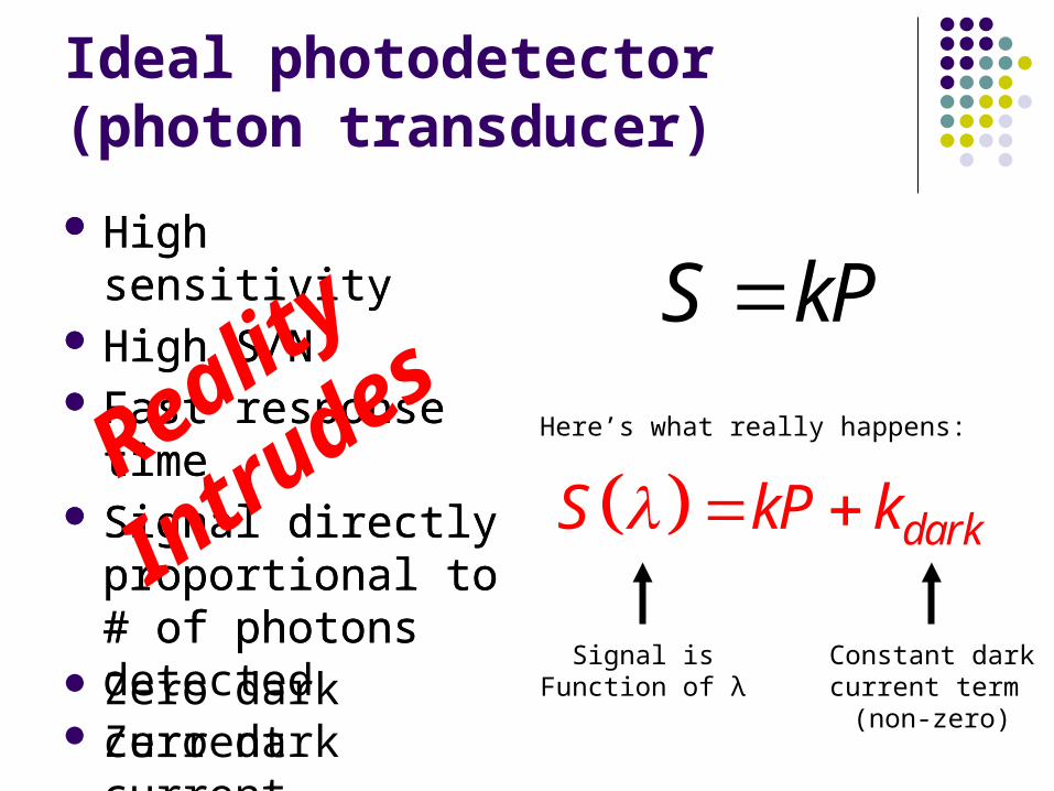
Ideal photodetector (photon transducer)
High sensitivity High S/N Fast response time Signal directly
proportional to # of photons
Zero dark current
S kP
darkS kP k Reality
Intrudes
Here’s what really happens:
Signal isFunction of λ
Constant darkcurrent term (non-zero)
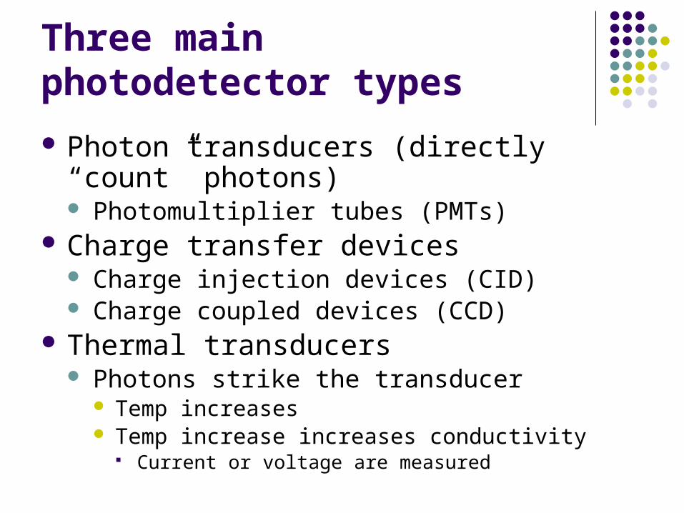
Three mainphotodetector types
Photon transducers (directly “count” photons) Photomultiplier tubes (PMTs)
Charge transfer devices Charge injection devices (CID) Charge coupled devices (CCD)
Thermal transducers Photons strike the transducer
Temp increases Temp increase increases conductivity
Current or voltage are measured
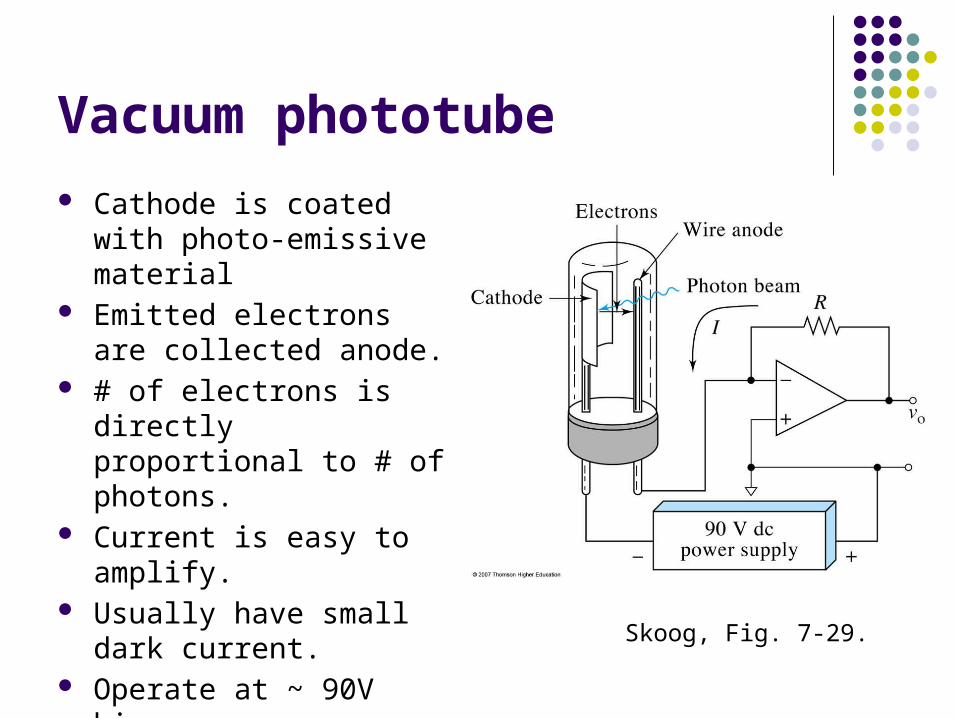
Vacuum phototube
Cathode is coated with photo-emissive material
Emitted electrons are collected anode.
# of electrons is directly proportional to # of photons.
Current is easy to amplify. Usually have small dark
current. Operate at ~ 90V bias Not so portable
Skoog, Fig. 7-29.
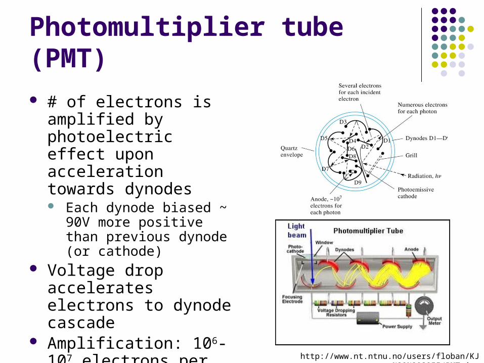
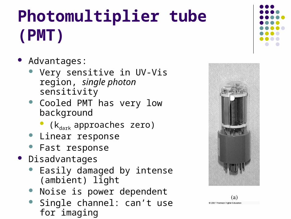
Photomultiplier tube (PMT) # of electrons is amplified
by photoelectric effect upon acceleration towards dynodes Each dynode biased ~ 90V
more positive than previous dynode (or cathode)
Voltage drop accelerates electrons to dynode cascade
Amplification: 106-107 electrons per incident photon; electron cascade
http://www.nt.ntnu.no/users/floban/KJ%20%203055/PMT.jpg
Photomultiplier tube (PMT) Advantages:
Very sensitive in UV-Vis region, single photon sensitivity
Cooled PMT has very low background (kdark approaches zero)
Linear response Fast response
Disadvantages Easily damaged by intense (ambient)
light Noise is power dependent Single channel: can’t use for imaging
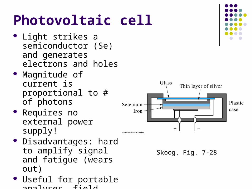
Photovoltaic cell Light strikes a
semiconductor (Se) and generates electrons and holes
Magnitude of current is proportional to # of photons
Requires no external power supply!
Disadvantages: hard to amplify signal and fatigue (wears out)
Useful for portable analyses, field work, outdoor setting
Skoog, Fig. 7-28
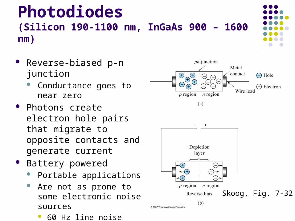
Photodiodes(Silicon 190-1100 nm, InGaAs 900 – 1600 nm)
Reverse-biased p-n junction Conductance goes to near
zero Photons create electron hole
pairs that migrate to opposite contacts and generate current
Battery powered Portable applications Are not as prone to some
electronic noise sources 60 Hz line noise
Skoog, Fig. 7-32
Multichannel transducers
Allow simultaneous interrogation of multiple wavelengths
Imaging Photodiode arrays (1-D array) Charge-transfer devices (2-D array)
Charge-injection devices Charge-coupled device (CCD) CMOS
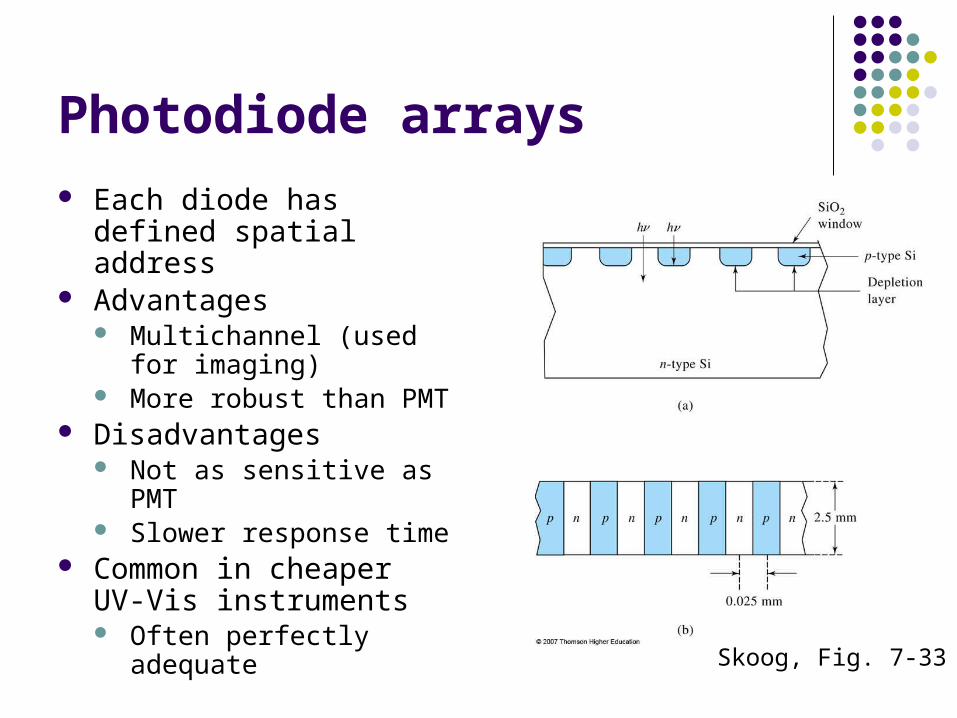
Photodiode arrays Each diode has defined
spatial address Advantages
Multichannel (used for imaging)
More robust than PMT Disadvantages
Not as sensitive as PMT Slower response time
Common in cheaper UV-Vis instruments Often perfectly adequate
Skoog, Fig. 7-33
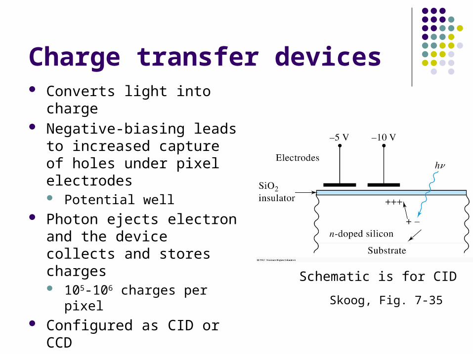
Charge transfer devices Converts light into charge Negative-biasing leads to
increased capture of holes under pixel electrodes Potential well
Photon ejects electron and the device collects and stores charges 105-106 charges per pixel
Configured as CID or CCD
Skoog, Fig. 7-35
Schematic is for CID
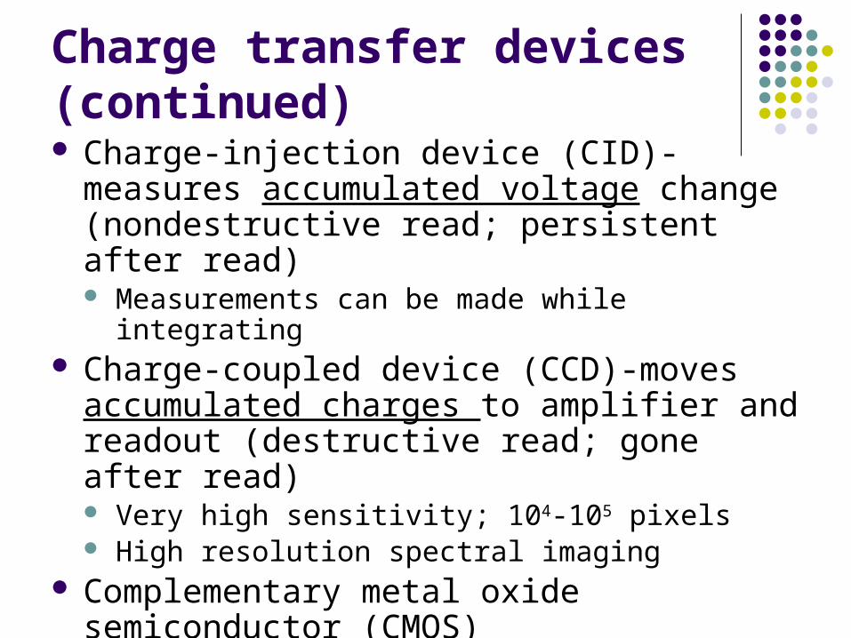
Charge transfer devices (continued) Charge-injection device (CID)-measures
accumulated voltage change (nondestructive read; persistent after read) Measurements can be made while integrating
Charge-coupled device (CCD)-moves accumulated charges to amplifier and readout (destructive read; gone after read) Very high sensitivity; 104-105 pixels High resolution spectral imaging
Complementary metal oxide semiconductor (CMOS) Webcam technology: CHEAP! OK sensitivity, large pixel density
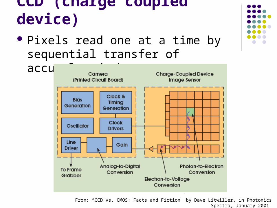
CCD (charge coupled device) Pixels read one at a time by sequential
transfer of accumulated charge
From: “CCD vs. CMOS: Facts and Fiction” by Dave Litwiller, in Photonics Spectra, January 2001
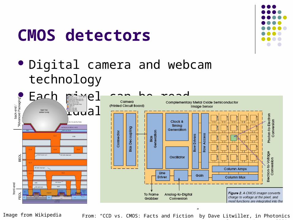
CMOS detectors
Digital camera and webcam technology Each pixel can be read individually
From: “CCD vs. CMOS: Facts and Fiction” by Dave Litwiller, in Photonics Spectra, January 2001 Image from Wikipedia
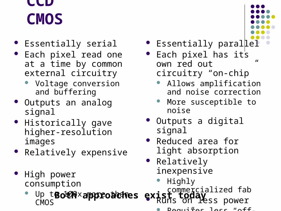
CCD CMOS Essentially serial Each pixel read one at a
time by common external circuitry Voltage conversion and
buffering Outputs an analog signal Historically gave higher-
resolution images Relatively expensive
High power consumption Up to 100x more than
CMOS
Essentially parallel Each pixel has its own red
out circuitry “on-chip” Allows amplification and
noise correction More susceptible to noise
Outputs a digital signal Reduced area for light
absorption Relatively inexpensive
Highly commercialized fab Runs on less power
Requires less “off-chip” circuitry
Both approaches exist today
Photoconductivity transducers
Semiconductors whose resistance decreases when they absorb light
Absorption promotes electron to conduction band.
Useful in near IR( = 0.75 to 3 m) Cooling allows extension to longer
wavelengths by reducing thermal noise
Thermal transducers
Solution for IR region (low energy photons) Thermocouples
Light absorbed heats the junction (two pieces of dissimilar metal) which leads to a change in voltage relative to a reference thermocouple.
Bolometer (thermistor) Material changes resistance as a function of temp
Pyroelectric devices Temperature-dependent capacitor Change in temperature leads to change in circuit current