Embed Size (px)
Citation preview
NATO LECTURES
M. Meyyappan
Introduction to Nanotechnology
Abstract
Nanotechnology deals with creation of materials, devices and systems in the nanometer
scale (1-100 nm) through manipulating matter at that scale and exploiting novel
properties arising because of the nanoscale. This lecture will first define
nanotechnology, particularly describing what it is and what it is not, followed by detailed
examples of change in various properties seen by going from bulk to nanoscale. The
effect of nanoscale on physical properties, bandgap, etc. will be illustrated. Examples of
novel nanomaterials such as nanotubes, nanowires, nanoparticles, etc. will be
introduced. Also, the tools used in nanotechnology research such as the scanning probe
microscopes, scanning tunneling microscopes etc. will be mentioned and a summary of
top-down and bottom-up processes needed in manufacturing will be presented as an
introduction to the more detailed coverage later. Finally, a broad overview of the
potential of nanotechnology on a sector-by-sector basis will be given to set the stage for
the subsequent lectures in this NATO series.
Nanotechnology deals with creation of materials, devices and systems through
manipulation of matter at the nanometer length scale. The object created itself does not
have to be nanoscale, but can be micro or macro size. What is critical is the ability to
exploit the novel properties that arise because of nanometer length scale. Indeed when
we go down from bulk to nanoscale, physical, chemical, mechanical, electrical, optical,
magnetic and other properties change. The field is about making use of such changes and
developing novel products and processes which have not been possible until now.
RTO-EN-AVT-129bis 1 - 1
Meyyappan, M. (2007) Introduction to Nanotechnology. In Nanotechnology Aerospace Applications – 2006 (pp. 1-1 – 1-2). Educational Notes RTO-EN-AVT-129bis, Paper 1. Neuilly-sur-Seine, France: RTO. Available from: http://www.rto.nato.int/abstracts.asp.
Report Documentation Page Form ApprovedOMB No. 0704-0188
Public reporting burden for the collection of information is estimated to average 1 hour per response, including the time for reviewing instructions, searching existing data sources, gathering andmaintaining the data needed, and completing and reviewing the collection of information. Send comments regarding this burden estimate or any other aspect of this collection of information,including suggestions for reducing this burden, to Washington Headquarters Services, Directorate for Information Operations and Reports, 1215 Jefferson Davis Highway, Suite 1204, ArlingtonVA 22202-4302. Respondents should be aware that notwithstanding any other provision of law, no person shall be subject to a penalty for failing to comply with a collection of information if itdoes not display a currently valid OMB control number.
1. REPORT DATE 01 MAR 2007
2. REPORT TYPE N/A
3. DATES COVERED -
4. TITLE AND SUBTITLE Introduction to Nanotechnology
5a. CONTRACT NUMBER
5b. GRANT NUMBER
5c. PROGRAM ELEMENT NUMBER
6. AUTHOR(S) 5d. PROJECT NUMBER
5e. TASK NUMBER
5f. WORK UNIT NUMBER
7. PERFORMING ORGANIZATION NAME(S) AND ADDRESS(ES) MM Associates Mail stop 229-3 Bldg 229, Room 214 Moffett Field, CA94035 UNITED STATES
8. PERFORMING ORGANIZATIONREPORT NUMBER
9. SPONSORING/MONITORING AGENCY NAME(S) AND ADDRESS(ES) 10. SPONSOR/MONITOR’S ACRONYM(S)
11. SPONSOR/MONITOR’S REPORT NUMBER(S)
12. DISTRIBUTION/AVAILABILITY STATEMENT Approved for public release, distribution unlimited
13. SUPPLEMENTARY NOTES See also ADM002060., The original document contains color images.
14. ABSTRACT
15. SUBJECT TERMS
16. SECURITY CLASSIFICATION OF: 17. LIMITATION OF ABSTRACT
SAR
18. NUMBEROF PAGES
41
19a. NAME OFRESPONSIBLE PERSON
a. REPORT unclassified
b. ABSTRACT unclassified
c. THIS PAGE unclassified
Standard Form 298 (Rev. 8-98) Prescribed by ANSI Std Z39-18
The advent of scanning tunneling microscope and atomic force microscope in the 1980s
has essentially ushered in the nano era. With these powerful tools, scientists were able to
see nature at the atomic level. Simultaneously, with increased computing power
available, modeling and simulation enabled an understanding of properties at the
nanoscale. This powerful combination of atomic scale characterization and detailed
modeling has led to the explosion we see today in nanoscale science and technology
research.
Nanoscale materials have a large surface area for a given volume. The surface properties
dominate compared to bulk properties. Quantum phenomena becomes critical at reduced
length scales. In most cases, the change in behavior is not a simple extrapolation of bulk
behavior as we know. In materials where strong chemical bonding is present, delocation
of valence electrons can be extensive. The extent of delocalization can vary with the size
of the system. Structure also changes with the size. These two changes can lead to
different physical and chemical properties depending on size, for example, magnetic,
optical properties, melting point, specific heat, surface reactivity, bandgap, etc.
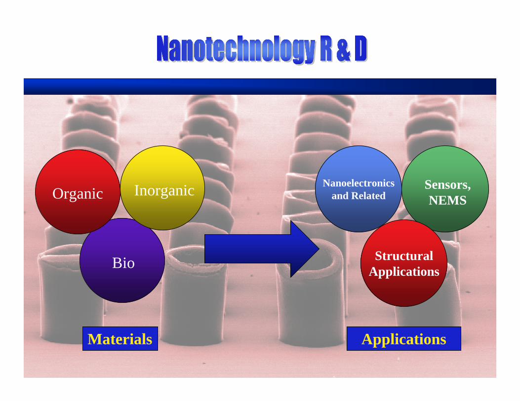
Nanomaterials currently under investigation include nanoparticles, nanotubes, nanowires,
powders, quantum dots, nanoporous materials, dendrimers, nanofibers, fullerenes, etc.
Examples of each of these will be discussed in the presentation. The application range
for these materials is very broad from electronics, sensors, electromechanical systems to
composites, coatings and lubricants.
Introduction to Nanotechnology
1 - 2 RTO-EN-AVT-129bis
M. Meyyappan
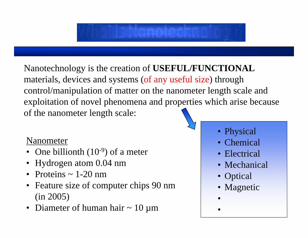
Nanotechnology is the creation of USEFUL/FUNCTIONALmaterials, devices and systems (of any useful size) through control/manipulation of matter on the nanometer length scale andexploitation of novel phenomena and properties which arise because of the nanometer length scale:
• Physical• Chemical• Electrical• Mechanical• Optical• Magnetic••
Nanometer• One billionth (10-9) of a meter• Hydrogen atom 0.04 nm• Proteins ~ 1-20 nm• Feature size of computer chips 90 nm
(in 2005)• Diameter of human hair ~ 10 µm
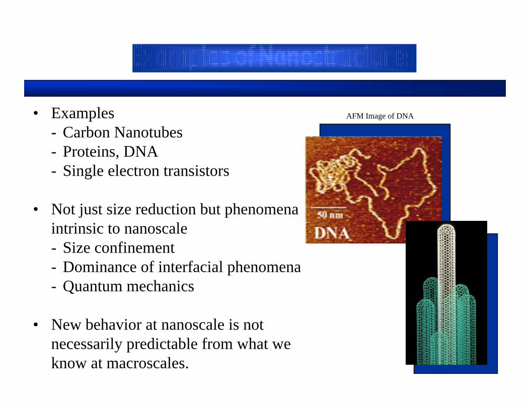
• Examples- Carbon Nanotubes- Proteins, DNA- Single electron transistors
• Not just size reduction but phenomena intrinsic to nanoscale- Size confinement- Dominance of interfacial phenomena- Quantum mechanics
• New behavior at nanoscale is not necessarily predictable from what we know at macroscales.
AFM Image of DNA
• Atoms and molecules are generally less than a nm and we study them in chemistry. Condensed matter physics deals with solidswith infinite array of bound atoms. Nanoscience deals with thein-between meso-world
• Quantum chemistry does not apply (although fundamental lawshold) and the systems are not large enough for classical laws ofphysics
• Size-dependent properties• Surface to volume ratio
- A 3 nm iron particle has 50% atoms on the surface- A 10 nm particle 20% on the surface- A 30 nm particle only 5% on the surface
• Many existing technologies already depend on nanoscale materialsand processes
- photography, catalysts are “old” examples- developed empirically decades ago
• In existing technologies using nanomaterials/processes, role ofnanoscale phenomena not understood until recently; serendipitousdiscoveries
- with understanding comes opportunities for improvement
• Ability to design more complex systems in the future is ahead- designer material that is hard and strong but low weight- self-healing materials
• Recently, there has been an explosion of research on the nanoscale behavior- Nanostructures through sub-micron self
assembly creating entities from “bottom-up”instead of “top-down”
- Characterization and applications- Highly sophisticated computer simulations to
enhance understanding as well as create ‘designer materials’
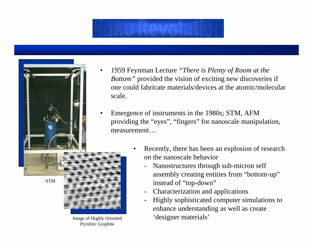
• 1959 Feynman Lecture “There is Plenty of Room at the Bottom” provided the vision of exciting new discoveries if one could fabricate materials/devices at the atomic/molecular scale.
• Emergence of instruments in the 1980s; STM, AFMproviding the “eyes”, “fingers” for nanoscale manipulation, measurement…
STM
Image of Highly OrientedPyrolitic Graphite
Nanoelectronicsand Related
StructuralApplications
Sensors,NEMSOrganic Inorganic
Bio
Materials Applications
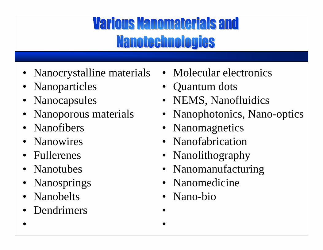
• Nanocrystalline materials• Nanoparticles• Nanocapsules• Nanoporous materials• Nanofibers• Nanowires• Fullerenes• Nanotubes• Nanosprings• Nanobelts• Dendrimers•
• Molecular electronics• Quantum dots• NEMS, Nanofluidics• Nanophotonics, Nano-optics• Nanomagnetics• Nanofabrication• Nanolithography• Nanomanufacturing• Nanomedicine• Nano-bio••
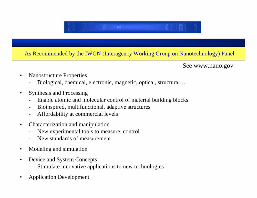
As Recommended by the IWGN (Interagency Working Group on Nanotechnology) Panel
• Nanostructure Properties- Biological, chemical, electronic, magnetic, optical, structural…
• Synthesis and Processing- Enable atomic and molecular control of material building blocks- Bioinspired, multifunctional, adaptive structures- Affordability at commercial levels
• Characterization and manipulation- New experimental tools to measure, control- New standards of measurement
• Modeling and simulation
• Device and System Concepts- Stimulate innovative applications to new technologies
• Application Development
See www.nano.gov
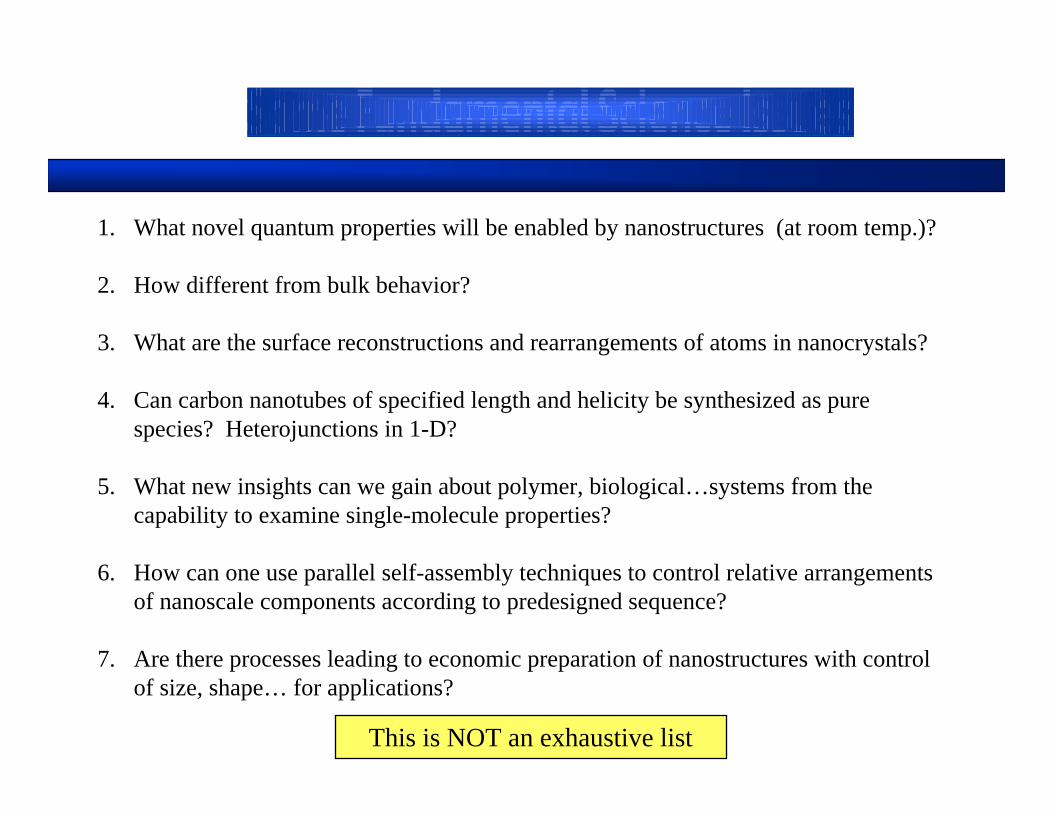
1. What novel quantum properties will be enabled by nanostructures (at room temp.)?
2. How different from bulk behavior?
3. What are the surface reconstructions and rearrangements of atoms in nanocrystals?
4. Can carbon nanotubes of specified length and helicity be synthesized as pure species? Heterojunctions in 1-D?
5. What new insights can we gain about polymer, biological…systems from the capability to examine single-molecule properties?
6. How can one use parallel self-assembly techniques to control relative arrangements of nanoscale components according to predesigned sequence?
7. Are there processes leading to economic preparation of nanostructures with control of size, shape… for applications?
This is NOT an exhaustive list
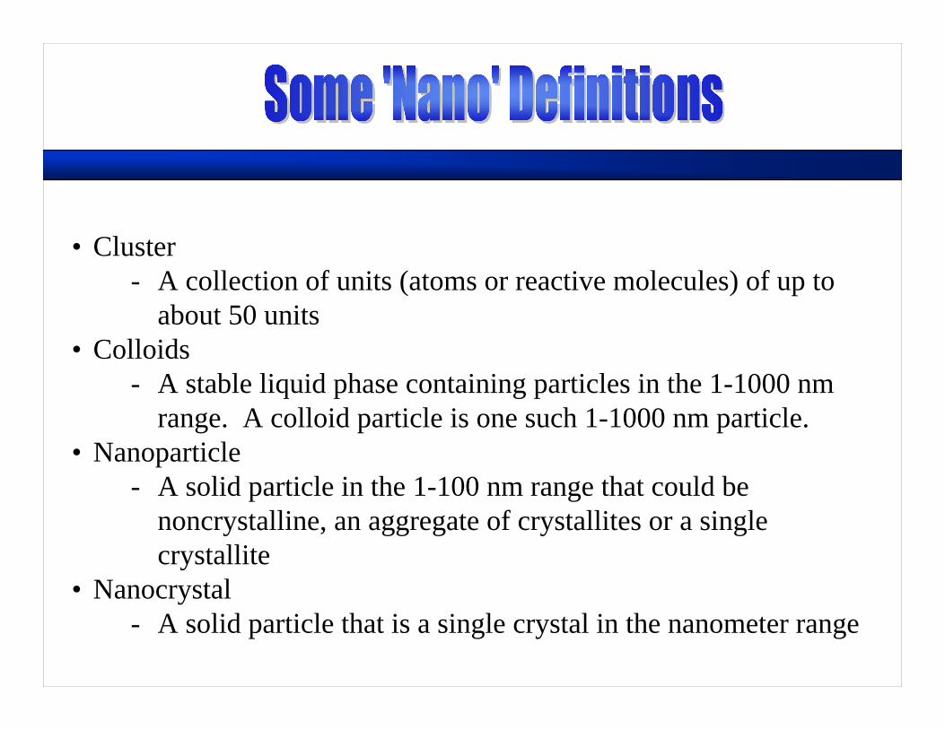
• Cluster- A collection of units (atoms or reactive molecules) of up to
about 50 units• Colloids
- A stable liquid phase containing particles in the 1-1000 nm range. A colloid particle is one such 1-1000 nm particle.
• Nanoparticle- A solid particle in the 1-100 nm range that could be
noncrystalline, an aggregate of crystallites or a single crystallite
• Nanocrystal- A solid particle that is a single crystal in the nanometer range
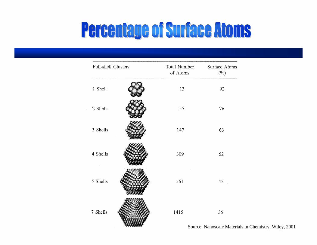
Source: Nanoscale Materials in Chemistry, Wiley, 2001
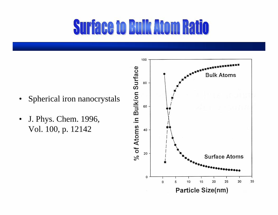
• Spherical iron nanocrystals
• J. Phys. Chem. 1996, Vol. 100, p. 12142
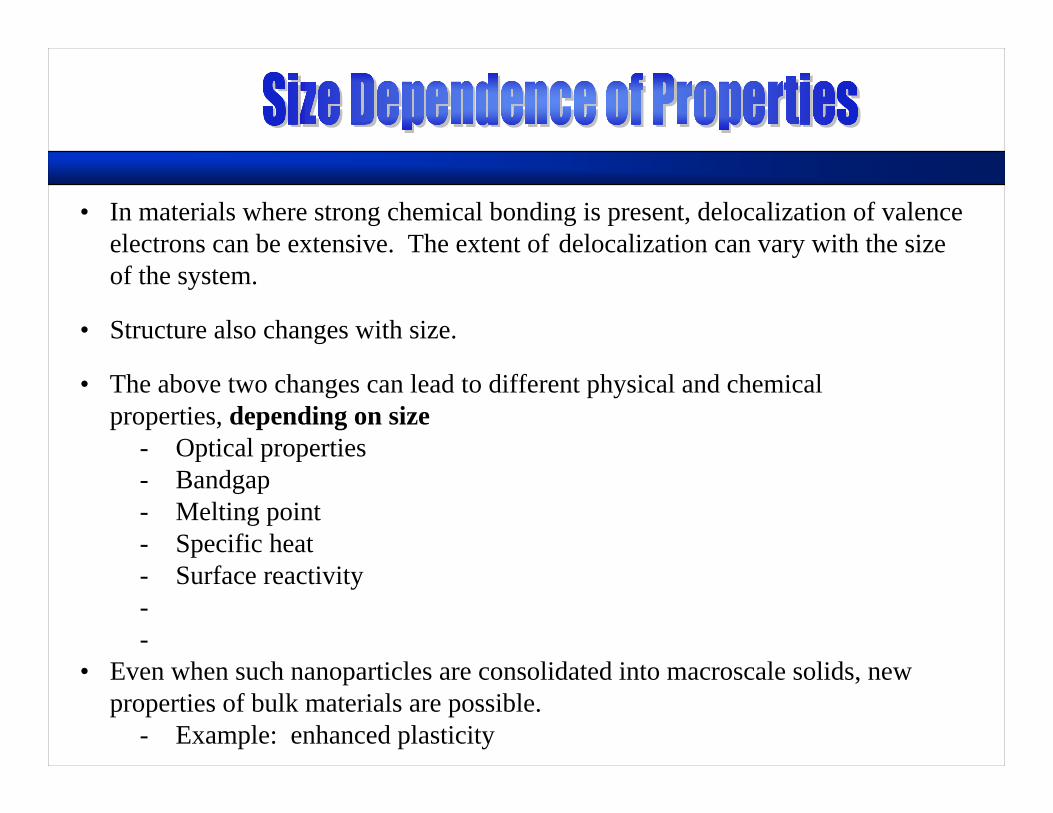
• In materials where strong chemical bonding is present, delocalization of valence electrons can be extensive. The extent of delocalization can vary with the size of the system.
• Structure also changes with size.
• The above two changes can lead to different physical and chemicalproperties, depending on size
- Optical properties- Bandgap- Melting point- Specific heat- Surface reactivity--
• Even when such nanoparticles are consolidated into macroscale solids, new properties of bulk materials are possible.
- Example: enhanced plasticity
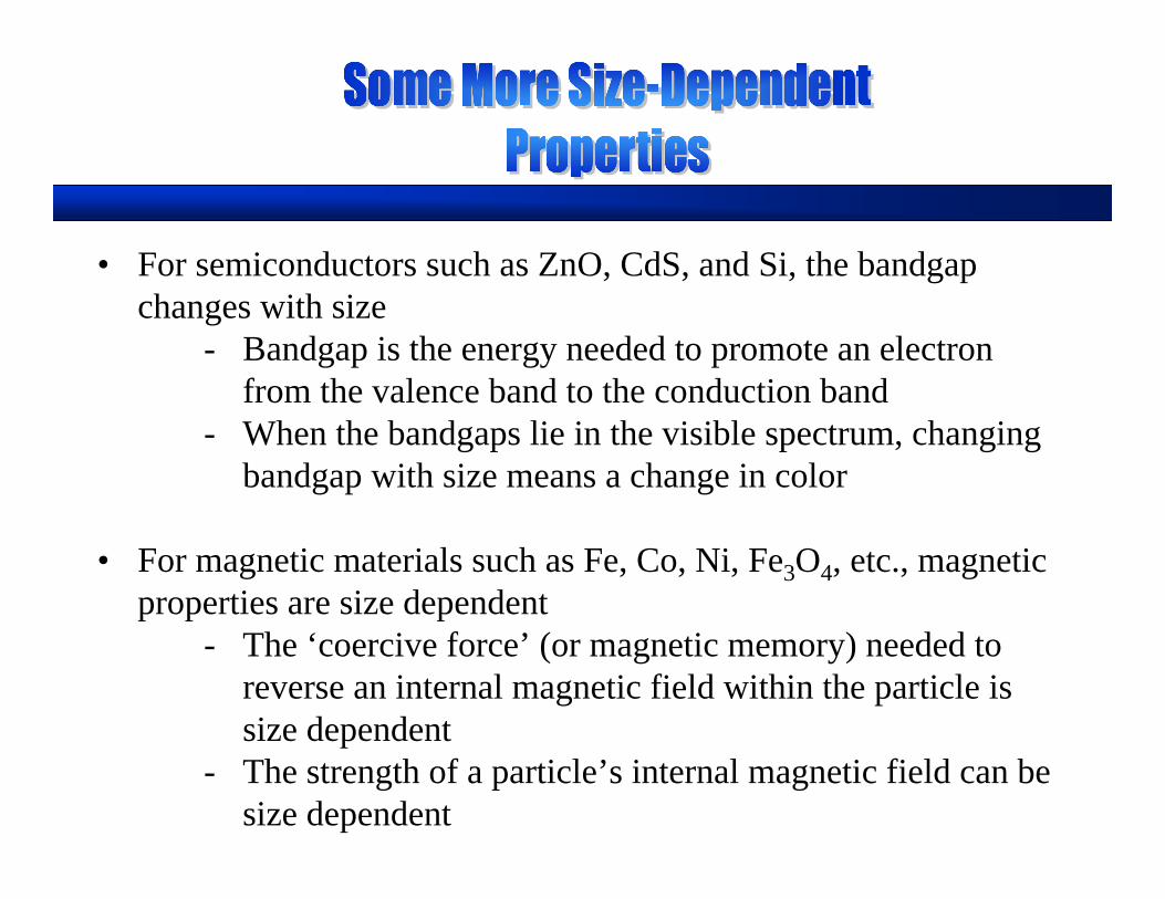
• For semiconductors such as ZnO, CdS, and Si, the bandgap changes with size
- Bandgap is the energy needed to promote an electron from the valence band to the conduction band
- When the bandgaps lie in the visible spectrum, changingbandgap with size means a change in color
• For magnetic materials such as Fe, Co, Ni, Fe3O4, etc., magnetic properties are size dependent
- The ‘coercive force’ (or magnetic memory) needed to reverse an internal magnetic field within the particle is size dependent
- The strength of a particle’s internal magnetic field can be size dependent
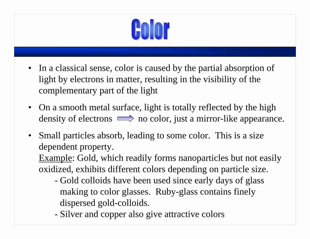
• In a classical sense, color is caused by the partial absorption of light by electrons in matter, resulting in the visibility of thecomplementary part of the light
• On a smooth metal surface, light is totally reflected by the high density of electrons no color, just a mirror-like appearance.
• Small particles absorb, leading to some color. This is a size dependent property.Example: Gold, which readily forms nanoparticles but not easily oxidized, exhibits different colors depending on particle size.
- Gold colloids have been used since early days of glass making to color glasses. Ruby-glass contains finely dispersed gold-colloids.
- Silver and copper also give attractive colors
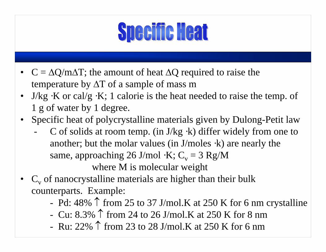
• C = ∆Q/m∆T; the amount of heat ∆Q required to raise the temperature by ∆T of a sample of mass m
• J/kg ·K or cal/g ·K; 1 calorie is the heat needed to raise the temp. of 1 g of water by 1 degree.
• Specific heat of polycrystalline materials given by Dulong-Petit law- C of solids at room temp. (in J/kg ·k) differ widely from one to
another; but the molar values (in J/moles ·k) are nearly the same, approaching 26 J/mol ·K; Cv = 3 Rg/M
where M is molecular weight• Cv of nanocrystalline materials are higher than their bulk
counterparts. Example:- Pd: 48% ↑ from 25 to 37 J/mol.K at 250 K for 6 nm crystalline- Cu: 8.3% ↑ from 24 to 26 J/mol.K at 250 K for 8 nm- Ru: 22% ↑ from 23 to 28 J/mol.K at 250 K for 6 nm
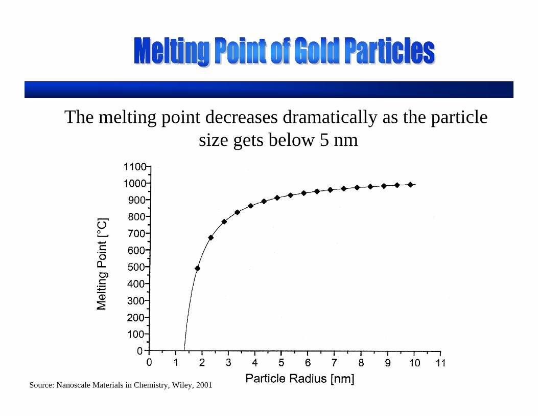
The melting point decreases dramatically as the particle size gets below 5 nm
Source: Nanoscale Materials in Chemistry, Wiley, 2001
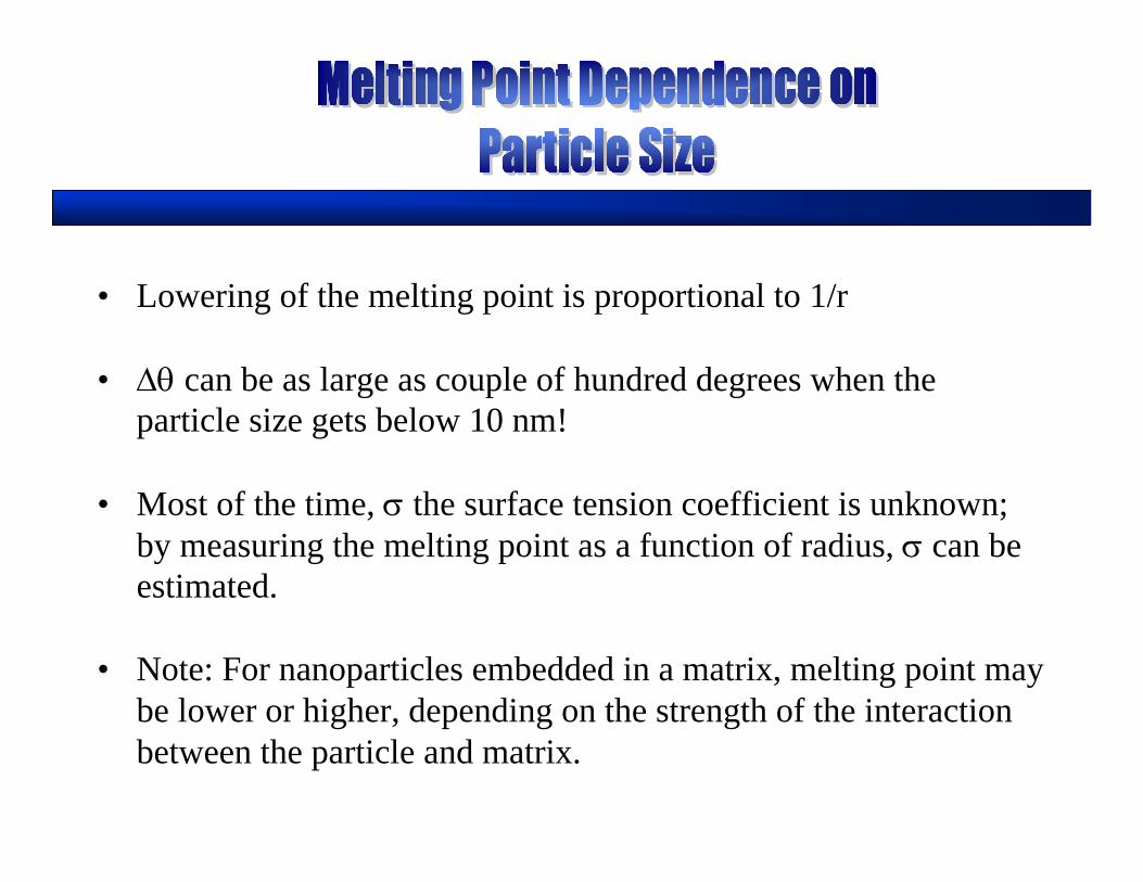
• Lowering of the melting point is proportional to 1/r
• Δθ can be as large as couple of hundred degrees when theparticle size gets below 10 nm!
• Most of the time, σ the surface tension coefficient is unknown;by measuring the melting point as a function of radius, σ can beestimated.
• Note: For nanoparticles embedded in a matrix, melting point maybe lower or higher, depending on the strength of the interactionbetween the particle and matrix.
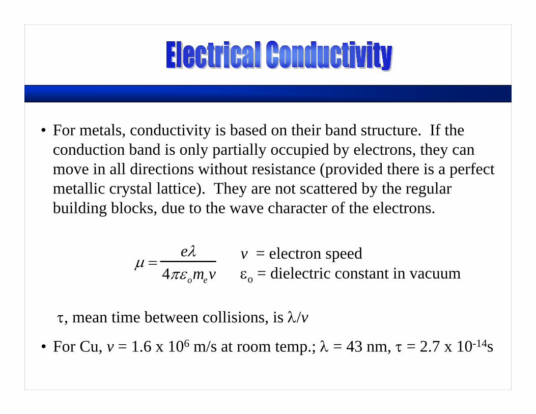
• For metals, conductivity is based on their band structure. If theconduction band is only partially occupied by electrons, they canmove in all directions without resistance (provided there is a perfectmetallic crystal lattice). They are not scattered by the regularbuilding blocks, due to the wave character of the electrons.
μ =eλ
4πεomevv = electron speedεo = dielectric constant in vacuum
τ, mean time between collisions, is λ/v
• For Cu, v = 1.6 x 10⁶ m/s at room temp.; λ = 43 nm, τ = 2.7 x 10⁻¹⁴s
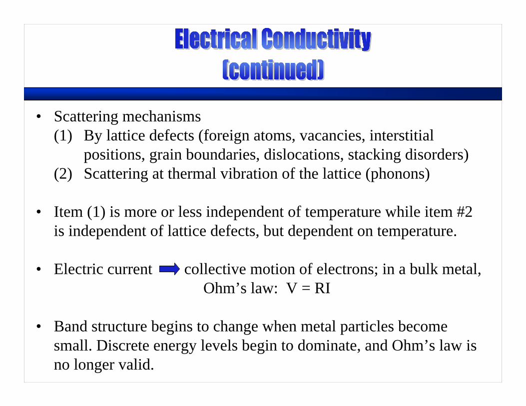
• Scattering mechanisms(1) By lattice defects (foreign atoms, vacancies, interstitial
positions, grain boundaries, dislocations, stacking disorders)(2) Scattering at thermal vibration of the lattice (phonons)
• Item (1) is more or less independent of temperature while item #2is independent of lattice defects, but dependent on temperature.
• Electric current collective motion of electrons; in a bulk metal,Ohm’s law: V = RI
• Band structure begins to change when metal particles becomesmall. Discrete energy levels begin to dominate, and Ohm’s law isno longer valid.
Source: Nanoscale Materials in Chemistry, Wiley, 2001
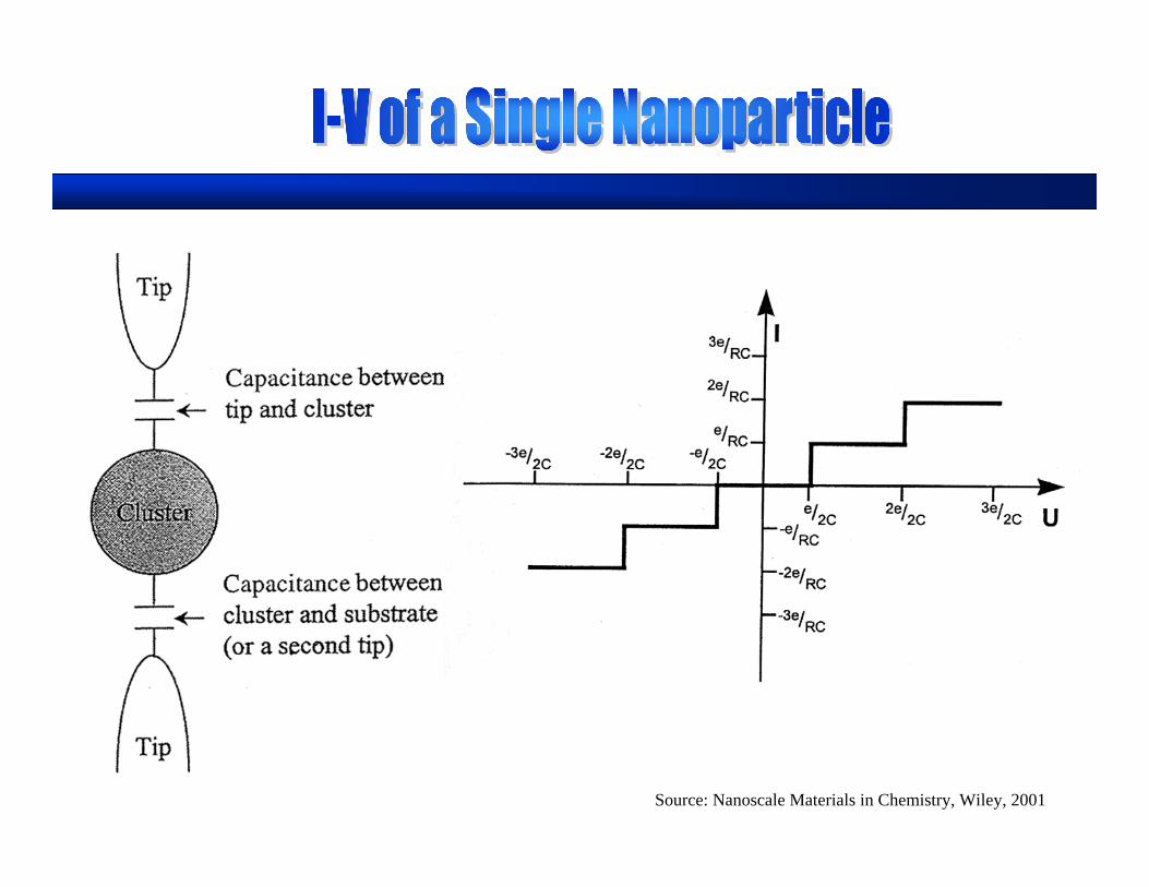
• Consider a single nanoparticle between two electrodes, but cushioned by a capacitance on each side
- If an electron is transferred to the particle, its coulomb energy byEc = e2/2c
- Thermal motion of the atoms in the particle can initiate a charge & Ec, leading to further electrons tunneling uncontrollably
- So, kT << e2/2c- Tunneling current I = V/RT- Current begins at coulomb voltage Vc = ± e/2c which is called coulomb
blockade- Further electron transfer happens if the coulomb energy of the ‘quantum
dot’ is compensated by an external voltage Vc = ± ne/2c where n is an integer
- Repeated tunneling results in a ‘staircase’ with step height in current, e/Rc
- Possible to charge and discharge a quantum dot in a quantized manner principle behind some future computers
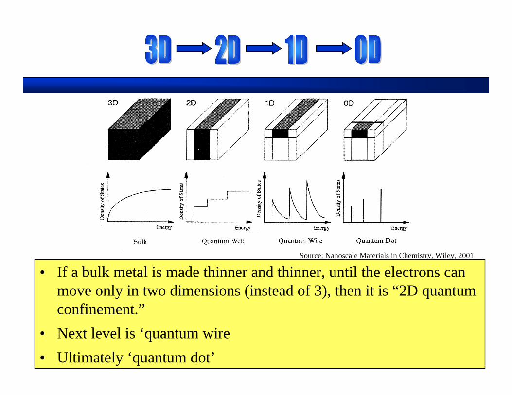
• If a bulk metal is made thinner and thinner, until the electrons can move only in two dimensions (instead of 3), then it is “2D quantum confinement.”
• Next level is ‘quantum wire• Ultimately ‘quantum dot’
Source: Nanoscale Materials in Chemistry, Wiley, 2001

Adsorption
• Adsorption is like absorption except the adsorbed material is held near the surface rather than inside
• Bulk solids, all molecules are surrounded by and bound to neighboring atoms and forces are in balance. Surface atoms are bound only on one side, leaving unbalanced atomic and molecular forces on the surface. These forces attract gases and molecules ⇒Van der Waals force, ⇒ physical adsorption or physisorption
• At high temperatures, unbalanced surface forces may be satisfied by electron sharing or valence bonding with gas atoms ⇒ chemical adsorption or chemisorption
- Basis for hetergeneous catalysis (key to production of fertilizers, pharmaceuticals, synthetic fibers, solvents, surfactants, gasolines, other fuels, automobile catalytic converters…)
- High specific surface area (area per unit mass)
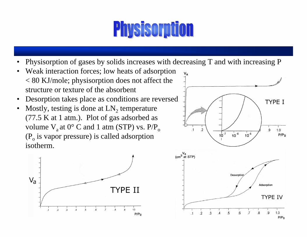
• Physisorption of gases by solids increases with decreasing T and with increasing P• Weak interaction forces; low heats of adsorption
< 80 KJ/mole; physisorption does not affect the structure or texture of the absorbent
• Desorption takes place as conditions are reversed• Mostly, testing is done at LN2 temperature
(77.5 K at 1 atm.). Plot of gas adsorbed as volume Va at 0° C and 1 atm (STP) vs. P/Po(Po is vapor pressure) is called adsorption isotherm.
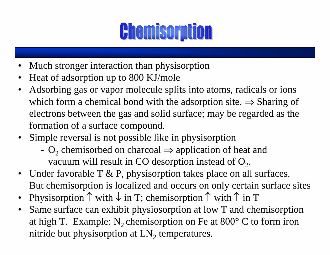
• Much stronger interaction than physisorption• Heat of adsorption up to 800 KJ/mole• Adsorbing gas or vapor molecule splits into atoms, radicals or ions
which form a chemical bond with the adsorption site. ⇒ Sharing of electrons between the gas and solid surface; may be regarded as the formation of a surface compound.
• Simple reversal is not possible like in physisorption- O2 chemisorbed on charcoal ⇒ application of heat and
vacuum will result in CO desorption instead of O2.• Under favorable T & P, physisorption takes place on all surfaces.
But chemisorption is localized and occurs on only certain surface sites• Physisorption ↑ with ↓ in T; chemisorption ↑ with ↑ in T• Same surface can exhibit physiosorption at low T and chemisorption
at high T. Example: N2 chemisorption on Fe at 800° C to form ironnitride but physisorption at LN2 temperatures.
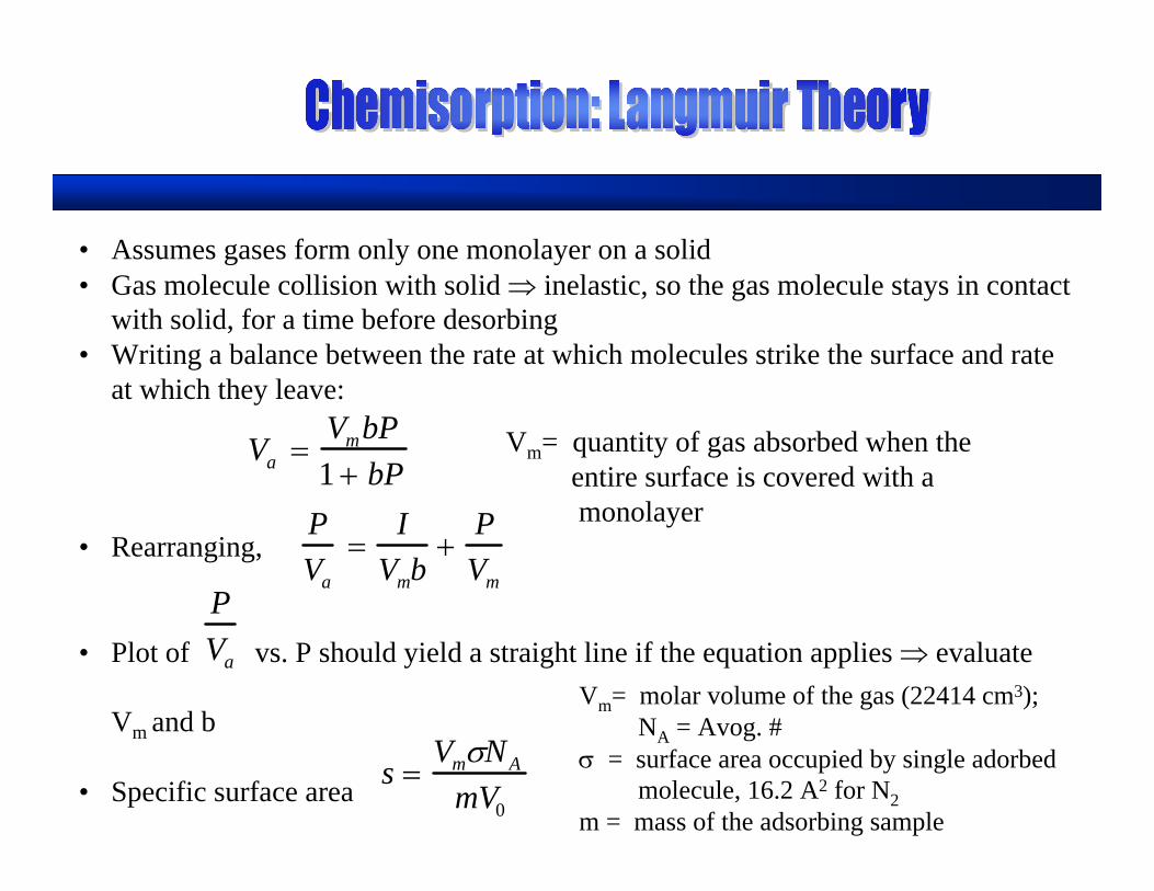
• Assumes gases form only one monolayer on a solid• Gas molecule collision with solid ⇒ inelastic, so the gas molecule stays in contact
with solid, for a time before desorbing• Writing a balance between the rate at which molecules strike the surface and rate
at which they leave:
Vm= quantity of gas absorbed when theentire surface is covered with a monolayer
• Rearranging,
• Plot of vs. P should yield a straight line if the equation applies ⇒ evaluate
Vm and b
• Specific surface area
Va =VmbP1 + bP
PVa
=I
Vmb+
PVm
PVa
s =VmσNA
mV0
Vm= molar volume of the gas (22414 cm3);NA = Avog. #
σ = surface area occupied by single adorbedmolecule, 16.2 A2 for N2
m = mass of the adsorbing sample
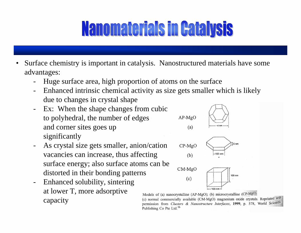
• Surface chemistry is important in catalysis. Nanostructured materials have someadvantages:
- Huge surface area, high proportion of atoms on the surface- Enhanced intrinsic chemical activity as size gets smaller which is likely
due to changes in crystal shape- Ex: When the shape changes from cubic
to polyhedral, the number of edgesand corner sites goes upsignificantly
- As crystal size gets smaller, anion/cationvacancies can increase, thus affecting surface energy; also surface atoms can be distorted in their bonding patterns
- Enhanced solubility, sinteringat lower T, more adsorptive capacity
• Zeolite is an old example which has been around a long time and used by petroleum industry as catalysts
• The surface area of a solid increases when it becomes nanoporous; this improves catalyst effects, adsorption properties
• ‘Adsorption’ is like ‘absorption’ except the absorbed material is held near the surface rather than inside
• How to make nanopores?- lithography followed by etching- ion beam etching/milling- electrochemical techniques- sol-gel techniques
• Frequently encountered powders:- Cement, fertilizer, face powder, table salt, sugar, detergents, coffee
creamer, baking soda…
• Some products in which powder incorporation is not obvious- Paint, tooth paste, lipstick, mascara, chewing gum, magnetic recording
media, slick magazine covers, floor coverings, automobile tires…
• For most applications, there is an optimum particle size- Taste of peanut butter affected by particle size- Extremely fine amorphous silica is added to control the ketchup flow- Medical tablets dissolve in our system at a rate controlled by particle size- Pigment size controls the saturation and brilliance of paints- Effectiveness of odor removers controlled by the surface area of
adsorbents.
From: Analytical methods in Fine Particle Technology, Webb and Orr
• Ability to synthesize nanoscale building blocks with control on size,composition etc. further assembling into larger structures withdesigned properties will revolutionize materials manufacturing- Manufacturing metals, ceramics, polymers, etc. at exact shapes without
machining- Lighter, stronger and programmable materials- Lower failure rates and reduced life-cycle costs- Bio-inspired materials- Multifunctional, adaptive materials- Self-healing materials
• Challenges ahead- Synthesis, large scale processing- Making useful, viable composites- Multiscale models with predictive capability- Analytical instrumentation
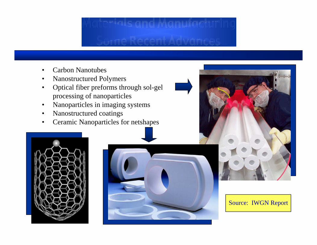
• Carbon Nanotubes• Nanostructured Polymers• Optical fiber preforms through sol-gel
processing of nanoparticles• Nanoparticles in imaging systems• Nanostructured coatings• Ceramic Nanoparticles for netshapes
Source: IWGN Report
• Nanostructured metals, ceramics at exact shapes without machining
• Improved color printing through better inks and dyes withnanoparticles
• Membranes and filters
• Coatings and paints (nanoparticles)
• Abrasives (using nanoparticles)
• Lubricants
• Composites (high strength, light weight)
• Catalysts
• Insulators
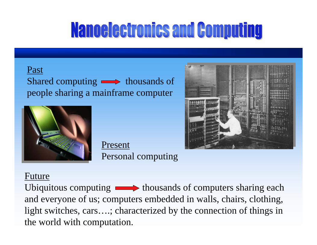
PastShared computing thousands of people sharing a mainframe computer
PresentPersonal computing
FutureUbiquitous computing thousands of computers sharing eachand everyone of us; computers embedded in walls, chairs, clothing,light switches, cars….; characterized by the connection of things inthe world with computation.
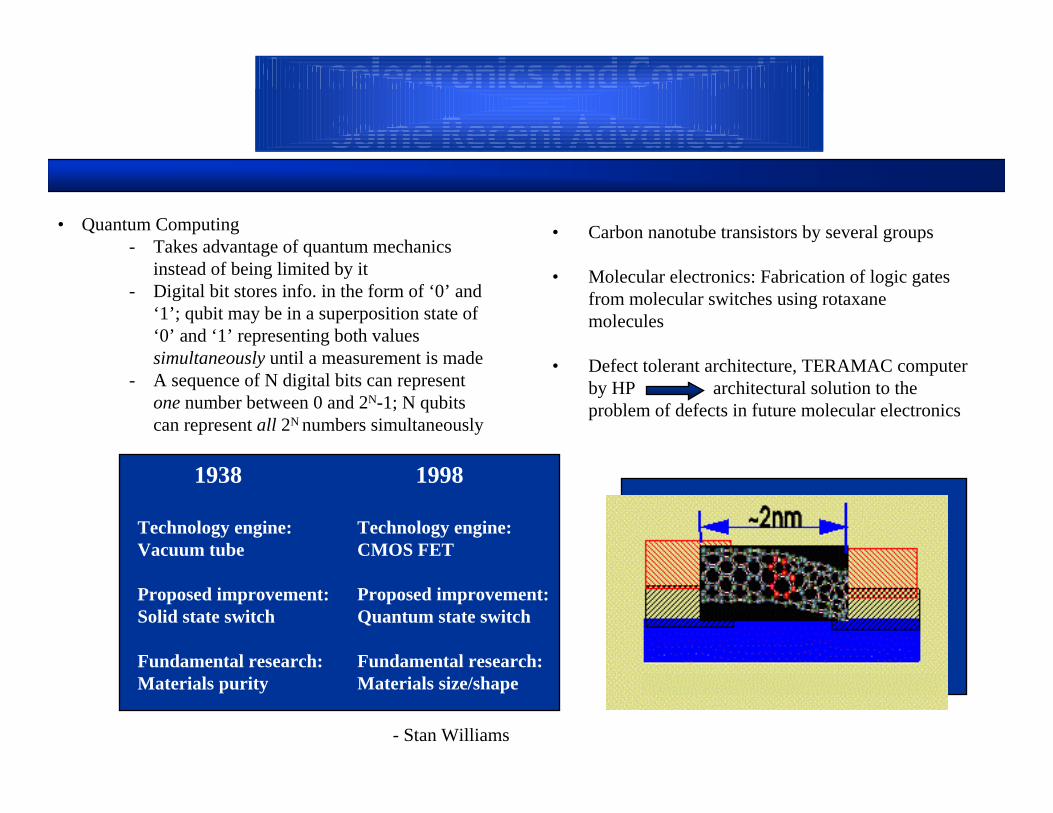
• Quantum Computing- Takes advantage of quantum mechanics
instead of being limited by it- Digital bit stores info. in the form of ‘0’ and
‘1’; qubit may be in a superposition state of ‘0’ and ‘1’ representing both valuessimultaneously until a measurement is made
- A sequence of N digital bits can represent one number between 0 and 2N-1; N qubits can represent all 2N numbers simultaneously
• Carbon nanotube transistors by several groups
• Molecular electronics: Fabrication of logic gatesfrom molecular switches using rotaxanemolecules
• Defect tolerant architecture, TERAMAC computerby HP architectural solution to theproblem of defects in future molecular electronics
1938 1998
Technology engine:Vacuum tube
Proposed improvement:Solid state switch
Fundamental research:Materials purity
Technology engine:CMOS FET
Proposed improvement:Quantum state switch
Fundamental research:Materials size/shape
- Stan Williams
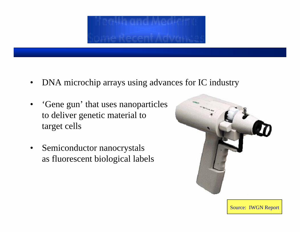
• DNA microchip arrays using advances for IC industry
• ‘Gene gun’ that uses nanoparticlesto deliver genetic material to target cells
• Semiconductor nanocrystalsas fluorescent biological labels
Source: IWGN Report
• Nanotechnology is not about simply shrinking the dimensions to1- 100 nm level nor is the routine top-down miniaturization as wedo in silicon CMOS fabrication. If that is the case, we do notneed new terminologies and funding to continue the old stuff.
• Instead, it is about exploring novel properties that arise becauseof the nanoscale - properties that differ from their bulkcounterparts.
• Once we identify such properties, the next big question is: Whatuseful things can we do with that?
• There are several areas in which researchers have been able toanswer positively to this question, leading to the evolution of thefield.