Embed Size (px)
Citation preview

Introduction to Multi‐gate MOSFETs
Tsu‐Jae King LiuDepartment of Electrical Engineering and Computer Sciences
University of California, Berkeley, CA 94720‐1770 USA
October 3, 2012
6th Annual SOI Fundamentals Class

MOSFET Fundamentals
Si substrate
Gate
Source Drain
GATE LENGTH, Lg
GATE OXIDE THICKNESS, Tox
0.25 micron MOSFET XTEM
http://www.eetimes.com/design/automotive‐design/4003940/LCD‐driver‐highly‐integrated
Metal Oxide SemiconductorField‐Effect Transistor:
2

MOSFET Operation: Gate Control• Current between Source and Drain is controlled by the Gate voltage.
gate oxide
P N+
Gate
N+
N‐channel MOSFET cross‐section
Desired characteristics:• High ON current• Low OFF current
Electron Energy Band Profile
increasing
E
distance
n(E) exp (‐E/kT)
SourceDrain
VDD
ION
IOFF
Inverse slope is subthreshold swing, S[mV/dec]
log ID
increasingVGS
VTHGATE VOLTAGE0
Leff
• “N‐channel” & “P‐channel” MOSFETs operate in a complementary manner“CMOS” = Complementary MOS
Source DrainBody
3

invD QvWI
DRAIN VOLTAGE, VDS
DRA
IN CURR
ENT, I D
)( THGSoxinv VVCQ effv
Substrate
Gate
Source Drain
MOSFET in ON State (VGS > VTH)
4
velocity inversion‐layer charge densitywidth
mobility gate overdrive
gate‐oxide capacitance
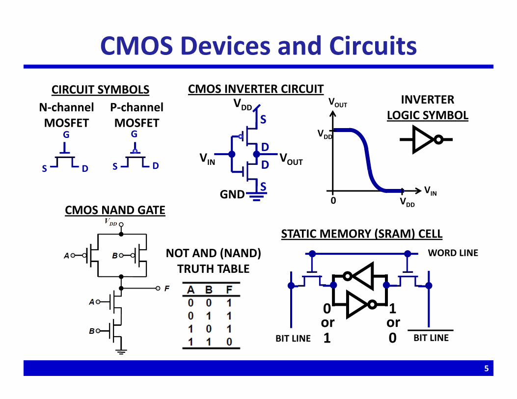
CMOS Devices and Circuits
0 1
1 0
STATIC MEMORY (SRAM) CELL
DS
G
DS
G
CIRCUIT SYMBOLSN‐channelMOSFET
P‐channelMOSFET
GND
VDDS
S
DD
CMOS INVERTER CIRCUIT
VIN VOUT
VOUT
VIN0 VDD
VDD
INVERTERLOGIC SYMBOL
BIT LINE
WORD LINE
BIT LINE
CMOS NAND GATE
NOT AND (NAND)TRUTH TABLE
5
or or
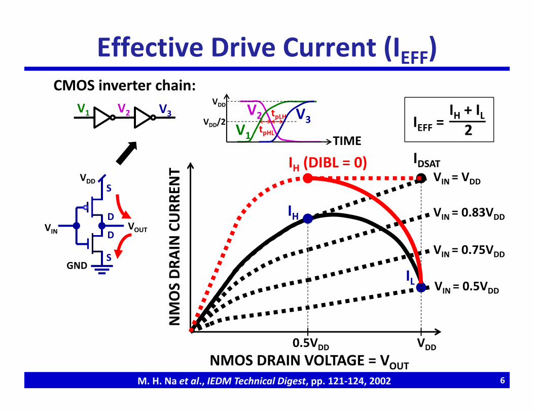
M. H. Na et al., IEDM Technical Digest, pp. 121‐124, 2002
NMOS DRAIN VOLTAGE = VOUT
VIN = VDD
VIN = 0.83VDD
VIN = 0.75VDD
VIN = 0.5VDD
NMOS DRA
IN CURR
ENT
IH
IL
VDD0.5VDD
IDSAT
V2
IH (DIBL = 0)
IEFF =IH + IL2tpHL
tpLHV1 TIME
VDD
VDD/2V1 V2 V3
CMOS inverter chain:
GND
VDDS
S
D
DVIN VOUT
V3
Effective Drive Current (IEFF)
6

log ID
VGSVDD
ION
• The greater the capacitive coupling between Gate and channel, the better control the Gate has over the channel potential.
Body
Gate
Drain
CoxCdep
higher ION/IOFF for fixed VDD, or lower VDD to achieve target ION/IOFFreduced drain‐induced barrier lowering (DIBL):
Source
Source Drainincreasing VDS
ox
total
CCS
log ID
VGS
increasing VDS
IOFF
Improving IEFF
7

CMOS Technology Scaling
• Gate length has not scaled proportionately with device pitch (0.7x per generation) in recent generations.– Transistor performance has been boosted by other means.
90 nm node 65 nm node 45 nm node 32 nm node
T. Ghani et al.,IEDM 2003
K. Mistry et al.,IEDM 2007
P. Packan et al.,IEDM 2009
XTEM images with the same scale courtesy V. Moroz (Synopsys, Inc.)
(after S. Tyagi et al., IEDM 2005)
8

P. Packan et al. (Intel), IEDM Technical Digest, pp. 659‐662, 2009
• Strained channel regions eff
• High‐k gate dielectric and metal gate electrodes Cox
Cross‐sectional TEM views of Intel’s 32 nm CMOS devices
MOSFET Performance Boosters
9

A. Asenov, Symp. VLSI Tech. Dig., p. 86, 2007
Process‐Induced Variations• Sub‐wavelength lithography:
– Resolution enhancement techniques are costly and increase process sensitivity
SiO2 Gate
Source Drain
A. Brown et al., IEEE Trans.Nanotechnology,p. 195, 2002
• Random dopant fluctuations (RDF):– Atomistic effects become
significant in nanoscale FETs
courtesy Mike Rieger (Synopsys, Inc.)
10
• Gate line‐edge roughness:photoresist

Bulk MOSFET Design Optimization• To maximize IEFF and minimize VTH variation, heavy doping
near the surface of the channel region should be avoided. Use a steep retrograde channel doping profile to suppress IOFF
SioxoxSi
oxSi
ox
Si
tttt
/12
oxSiox
Si tt2
Double-Gate FET
Scale length:
Ground-Plane FETStructure: Double-Gate FET
Scale length:
Ground-Plane FETStructure:
SourceDrain
Energy Band Profile:(OFF State)
longer
R.‐H. Yan et al., IEEE Trans. Electron Devices, Vol. 39, pp. 1704‐1710, 1992
• tSi is a critical design parameter!
11

Thin‐Body MOSFETs
Ultra‐Thin Body (UTB)
Buried Oxide
Si Substrate
Source Drain
Gate
tSi
Lg
Double‐Gate (DG)
Gate
Source Drain
Gate
tSi
Lg
R.‐H. Yan et al., IEEE TED 1992B. Yu et al., ISDRS 1997 12

Why Thin‐Body Structures?• Physically limit the depth of the channel region to eliminate sub‐surface leakage paths and achieve good electrostatic integrity
DrainSource
Gate
LgUltra‐Thin‐Body
MOSFET:
Buried Oxide
Source Drain
Gate
Substrate
“Silicon‐on‐Insulator” (SOI)
Wafer13
• Body doping can be eliminated if tSi is sufficiently thin higher ION due to higher carrier mobility reduced impact of random dopant fluctuations (RDF)

Effect of tSi on OFF‐state Leakage
IOFF = 19 A/mIOFF = 2.1 nA/mLeakage CurrentDensity [A/cm2]@ VDS = 0.7 V
106
10‐1
3x10²
0.0
4.0
8.0
12.0
16.0
20.0
G
G
S D
G
G
S D
Si Thickness [nm]
Lg = 25 nm; tox,eq = 12Å
tSi = 10 nm tSi = 20 nm
14

Relaxing the Body Thinness Requirement
O. Faynot, IEEE Int’l SOI Conference, 2011
• Thinner buried oxide (BOX) reduced DIBL• Reverse back biasing further reduction of SCE
15
Impact of BOX Thickness tSi Reduction with Lg Scaling

Threshold Voltage (VTH) Adjustment
T. Ohtou et al., IEEE‐EDL 28, p. 740, 2007
TBOX = 10nm
• VTH can be adjusted via substrate doping, for reduced VTH:
S. Mukhopadhyay et al., IEEE‐EDL 27, p. 284, 2006
• VTH can be adjusted via substrate doping, for reduced VTH:
• VTH can be dynamically adjusted via back‐biasing.– Reverse back biasing (to increase VTH) is beneficial for lowering SCE.
16

Double‐Gate MOSFET Structures
L. Geppert, IEEE Spectrum, October 2002 17
PLANAR:
VERTICAL FIN:

Double‐Gate “FinFET”
Planar DG‐FET
Gate
Source Drain
Gate
tSi
Fin Width = tSi
Lg
GATE
SOURCE
DRAIN20 nm
10 nmY.‐K. Choi et al., IEDM Technical Digest, 2001
15nm Lg FinFET:
Fin Height HFIN = W/2
D. Hisamoto et al., IEDM Technical Digest, 1998
N. Lindert et al., IEEE Electron Device Letters, p. 487, 2001
FinFET
Source
DrainGate
Lg
18

• Use spacers to define fins
Fin Patterning by Spacer Lithography
Fin
hard mask
spacer
Plan View
• Note that gate line‐edge roughness is not an issue for FinFETs
Y.‐K. Choi et al., IEEE Trans. Electron Devices, Vol. 49,pp. 436‐441, 2002
CD=1.3nm
CD=3.6nm
• Better CD control is achieved with spacer lithography
BOXSOI
3‐D Viewspacer resist
sacrificial
Gate
DrainSource
• Use spacers to define fins, and photoresist to define source/drain contact pad regions:
19

Impact of Fin Layout Orientation
(Series resistance is more significant at shorter Lg.)
• If the fin is oriented || or to the wafer flat, the channel surfaces lie along (110) planes.– Lower electron mobility– Higher hole mobility
• If the fin is oriented 45° to the wafer flat, the channel surfaces lie along (100) planes.
L. Chang et al., SISPAD, 2004 20

• The gate electrodes of a double‐gate FET can be isolated by a masked etch, to allow for separate biasing.– One gate is used for switching. – The other gate is used for VTH control.
Independent Gate Operation
Source
Drain Back‐Gated FET
Gate1Gate2
L. Mathew et al. (Freescale Semiconductor), 2004 IEEE International SOI Conference
D. M. Fried et al. (Cornell U.), IEEE Electron Device Letters, Vol. 25, pp. 199‐201, 2004
21

FinFET Layout• Layout is similar to that of conventional MOSFET, except
that the channel width is quantized:
Bulk‐Si MOSFET
Source
Drain
Source
Gate GateSource
Drain
SourceFinFET
Pfin
Intel Corp.
The S/D fins can be merged by selective epitaxy:
M. Guillorn et al., Symp. VLSI Technology 2008
22

• Fin Pitch– Limited by lithographic capability– Constrains source/drain implant tilt angle– Tradeoff: performance vs. layout efficiency
• Fin Width– Determines short‐channel effects
FinFET Design Trade‐Offs
Pfin
• Fin Height– Limited by etch technology– Tradeoff: layout efficiency
vs. design flexibility
Parasitic gate resistance and capacitance depend on Pfin
Source
DrainGate
Fin Width = tSi
Lg
Fin Height HFIN = W/2
23
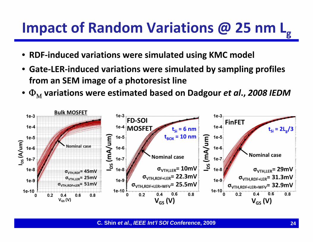
Impact of Random Variations @ 25 nm Lg• RDF‐induced variations were simulated using KMC model• Gate‐LER‐induced variations were simulated by sampling profiles from an SEM image of a photoresist line
• variations were estimated based on Dadgour et al., 2008 IEDM
24C. Shin et al., IEEE Int’l SOI Conference, 2009
tSi = 2Lg/3tSi = 6 nmtBOX = 10 nm

Multi‐gate MOSFETs
I. Ferain, C. A. Colinge, J.‐P. Colinge, Nature 479, 310–316 (2011)

SOI Multi‐Gate MOSFET Designs
after Yang and Fossum, IEEE Trans. Electron Devices, Vol. 52, pp. 1159‐1164, 2005
HSi/ L e
ff
WSi / Leff
body dimensions required forDIBL=100 mV/V
UTB FETUltra‐thin SOIHSi ~ Lg/5
FinFETNarrow finWSi ~ Lg/2
Tri‐Gate FETRelaxed fin dimensionsWSi > Lg/2; HSi > Lg/5
Tox = 1.1nm
26
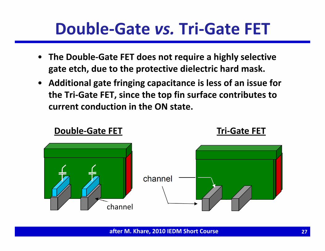
Double‐Gate vs. Tri‐Gate FET• The Double‐Gate FET does not require a highly selective
gate etch, due to the protective dielectric hard mask.• Additional gate fringing capacitance is less of an issue for
the Tri‐Gate FET, since the top fin surface contributes to current conduction in the ON state.
Double‐Gate FET Tri‐Gate FET
channel
after M. Khare, 2010 IEDM Short Course 27

22nm Tri‐Gate FETs
C. Auth et al., Symp. VLSI Technology 2012
• Lg = 30‐34 nm; Wfin = 8 nm; Hfin = 34 nm• High‐k/metal gate stack, EOT = 0.9 nm• Channel strain techniques
28
Transfer Characteristics
NMOSPMOS
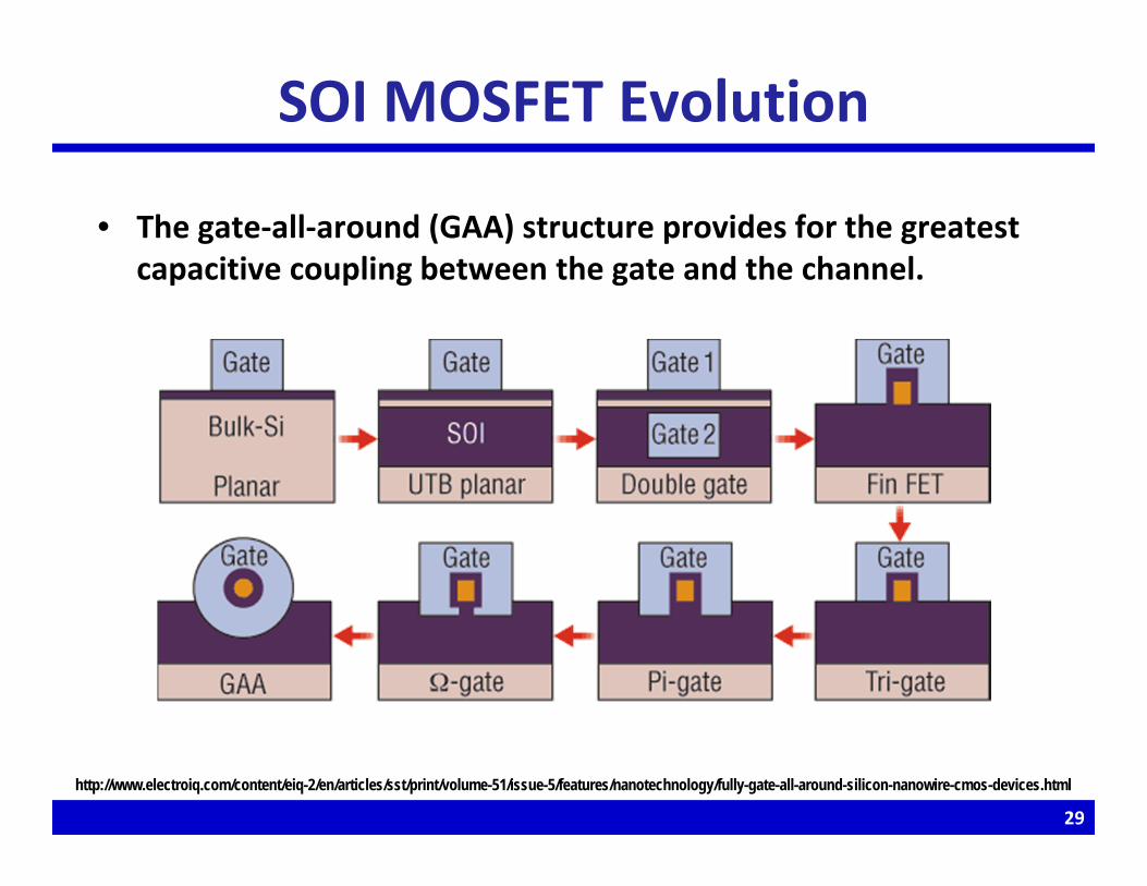
SOI MOSFET Evolution
• The gate‐all‐around (GAA) structure provides for the greatest capacitive coupling between the gate and the channel.
http://www.electroiq.com/content/eiq-2/en/articles/sst/print/volume-51/issue-5/features/nanotechnology/fully-gate-all-around-silicon-nanowire-cmos-devices.html
29

Summary
• Power density and variability now limit conventional bulk MOSFET scaling.
• Multi‐gate MOSFET structures can achieve superior electrostatic integrity than the conventional planar bulk MOSFET structure and hence offer a pathway to lower VDD, reduce VTH variability, and extend transistor scaling.
30