Embed Size (px)
Citation preview
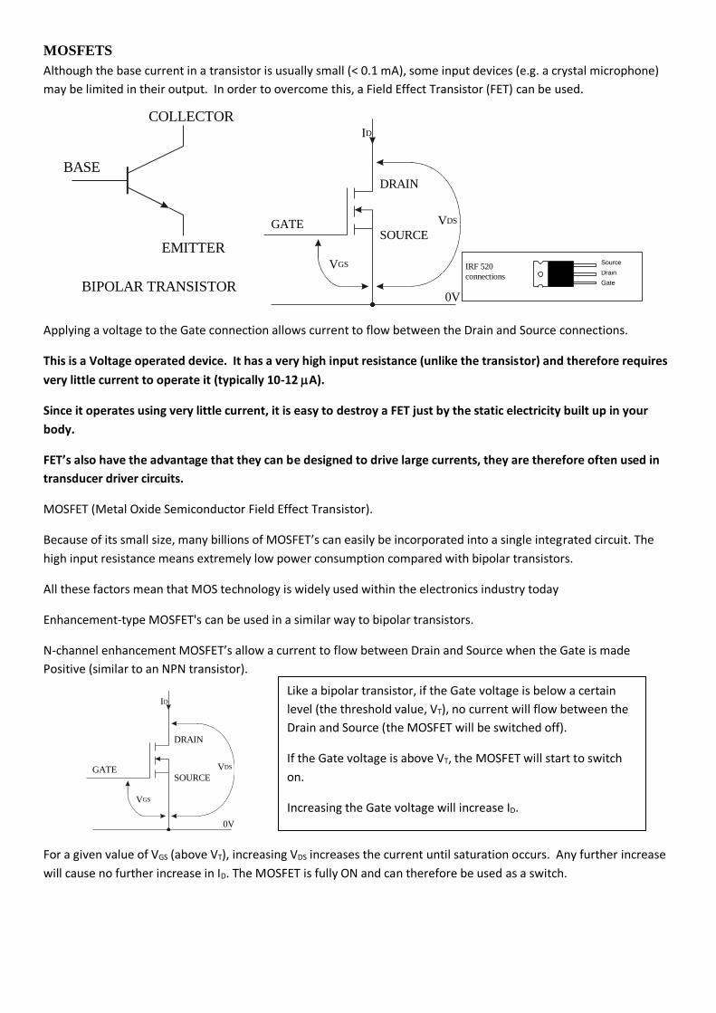
MOSFETS
Although the base current in a transistor is usually small (< 0.1 mA), some input devices (e.g. a crystal microphone)
may be limited in their output. In order to overcome this, a Field Effect Transistor (FET) can be used.
COLLECTOR
EMITTER
BASE
DRAIN
SOURCE
GATE
BIPOLAR TRANSISTOR FIELD EFFECTTRANSISTOR
GATE
DRAIN
SOURCE
ID
VGS
VDS
0V
Drain
Gate
SourceIRF 520
connections
Applying a voltage to the Gate connection allows current to flow between the Drain and Source connections.
This is a Voltage operated device. It has a very high input resistance (unlike the transistor) and therefore requires
very little current to operate it (typically 10-12 A).
Since it operates using very little current, it is easy to destroy a FET just by the static electricity built up in your
body.
FET’s also have the advantage that they can be designed to drive large currents, they are therefore often used in
transducer driver circuits.
MOSFET (Metal Oxide Semiconductor Field Effect Transistor).
Because of its small size, many billions of MOSFET’s can easily be incorporated into a single integrated circuit. The
high input resistance means extremely low power consumption compared with bipolar transistors.
All these factors mean that MOS technology is widely used within the electronics industry today
Enhancement-type MOSFET's can be used in a similar way to bipolar transistors.
N-channel enhancement MOSFET’s allow a current to flow between Drain and Source when the Gate is made
Positive (similar to an NPN transistor).
GATE
DRAIN
SOURCE
ID
VGS
VDS
0V
For a given value of VGS (above VT), increasing VDS increases the current until saturation occurs. Any further increase
will cause no further increase in ID. The MOSFET is fully ON and can therefore be used as a switch.
Like a bipolar transistor, if the Gate voltage is below a certain
level (the threshold value, VT), no current will flow between the
Drain and Source (the MOSFET will be switched off).
If the Gate voltage is above VT, the MOSFET will start to switch
on.
Increasing the Gate voltage will increase ID.
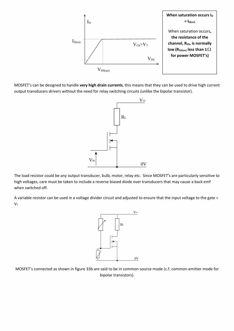
ID(on)
VDS(sat)
VGS>VT
VDS
ID
MOSFET’s can be designed to handle very high drain currents, this means that they can be used to drive high current
output transducers drivers without the need for relay switching circuits (unlike the bipolar transistor).
The load resistor could be any output transducer, bulb, motor, relay etc. Since MOSFET’s are particularly sensitive to
high voltages, care must be taken to include a reverse biased diode over transducers that may cause a back emf
when switched off.
A variable resistor can be used in a voltage divider circuit and adjusted to ensure that the input voltage to the gate =
VT
0V
RL
Vcc
MOSFET’s connected as shown in figure 33b are said to be in common-source mode (c.f. common-emitter mode for
bipolar transistors).
0V
RL
Vcc
Vin
When saturation occurs ID
= ID(on)
When saturation occurs,
the resistance of the
channel, RDS, is normally
low (RDS(on) less than 1
for power MOSFET’s)
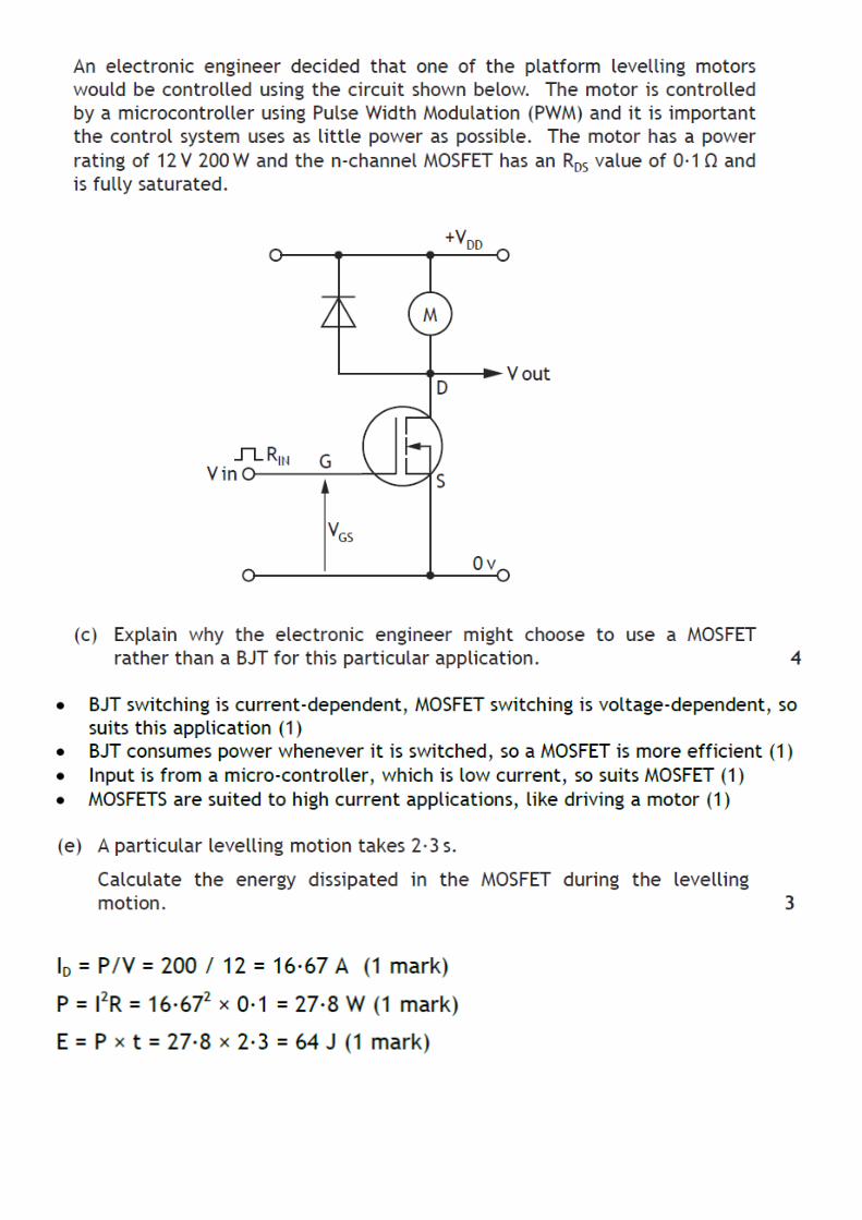
PRACTICAL ASSIGNMENT
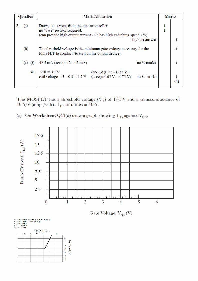
MOSFET characteristics - relationship between Drain current (ID) and Gate voltage (VGS)
Construct the circuit shown below using multimeters to measure the drain current and the gate voltage.
Adjusting the power supply will allow you to change VGS.
Construct a table for recording your results (as shown below).
VGS (V) ID (mA)
0.0
1.0
2.0
3.0
3.5
4.0
5.0
6.0
MOSFET
Symbol
mosfet
High Input
Resistance
zero current into gate/high gate resistance/voltage controlled.
The three are all related and all good. It means that the signal that is controlling the
FET is not affected by putting the FET in the circuit; a Bipolar Junction Transistor will
affect the input signal because of the current it draws.
Zero resistance at
output.
zero drain source resistance on saturation, except when given a resistance or Vds
Threshold Voltage The threshold voltage relates to the voltage that switches on the FET, Vt
BJT switching is current-dependent, MOSFET switching is voltage-dependent, so suits
switching on a large current with a voltage
BJT consumes power whenever it is switched, so a MOSFET is more efficient
Input is from a micro-controller, which is low current, so suits MOSFET
MOSFETS are suited to high current applications, like driving a motor
Static Sensitive A disadvantage of FETs is they are static sensitive; they can be destroyed by
handling. (The same goes for CMOS chips, they are made from MOSFETS)
Measure ID for various values of
VGS.
Find the threshold voltage for
this MOSFET
Plot a graph of ID against VGS and
calculate gm for this MOSFET.
GATE
DRAIN
SOURCE
I D
V GS
V DS
0V
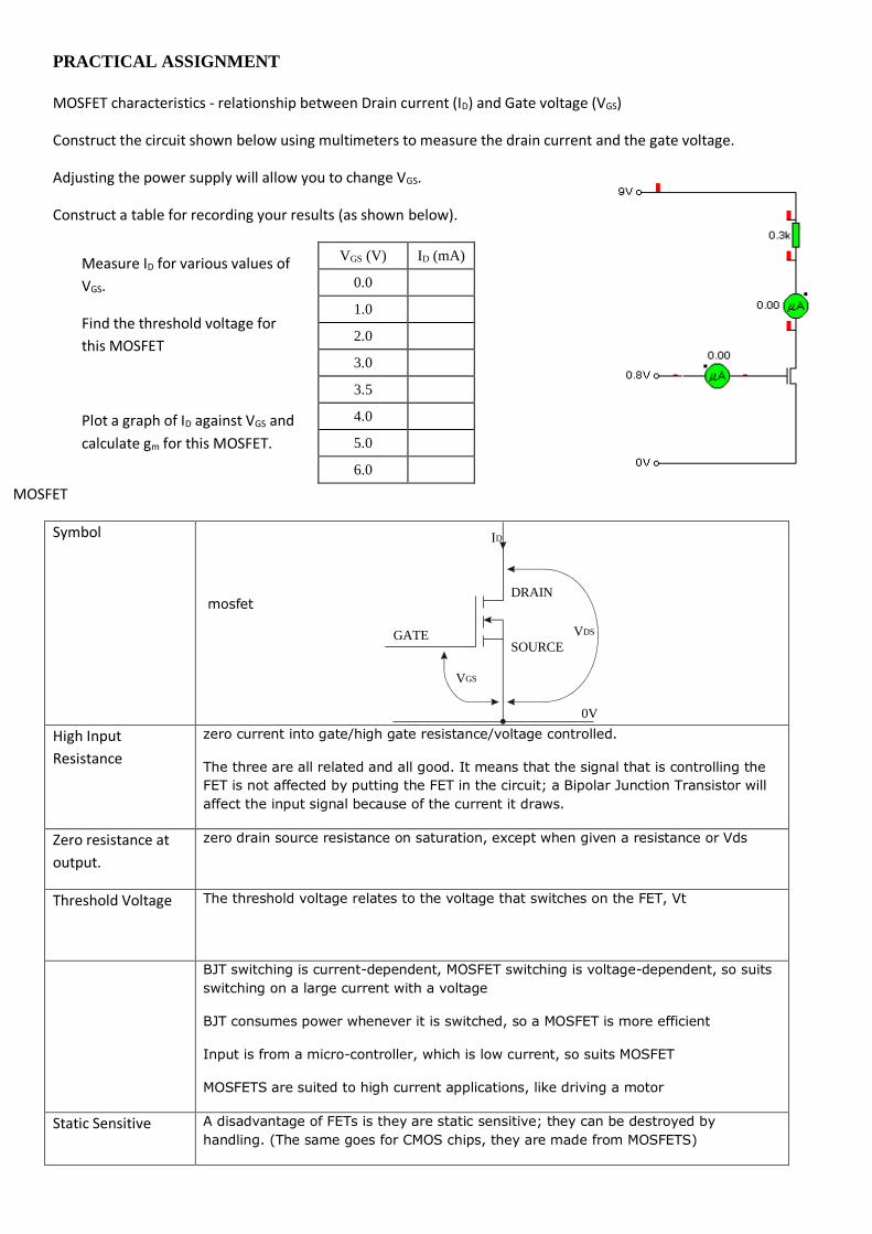
The image below is from the Data Book. In the exam there may be a similar graph with values on it ,
see the following questions for how it is used.
Transconductance is a measure of how the output current changes when the input voltage changes. A big
transcundance figure means a small change in the input voltage will lead to a large change in the output current.
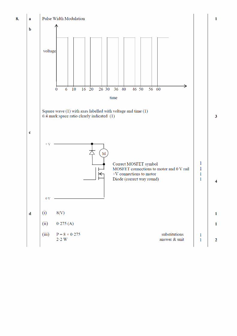
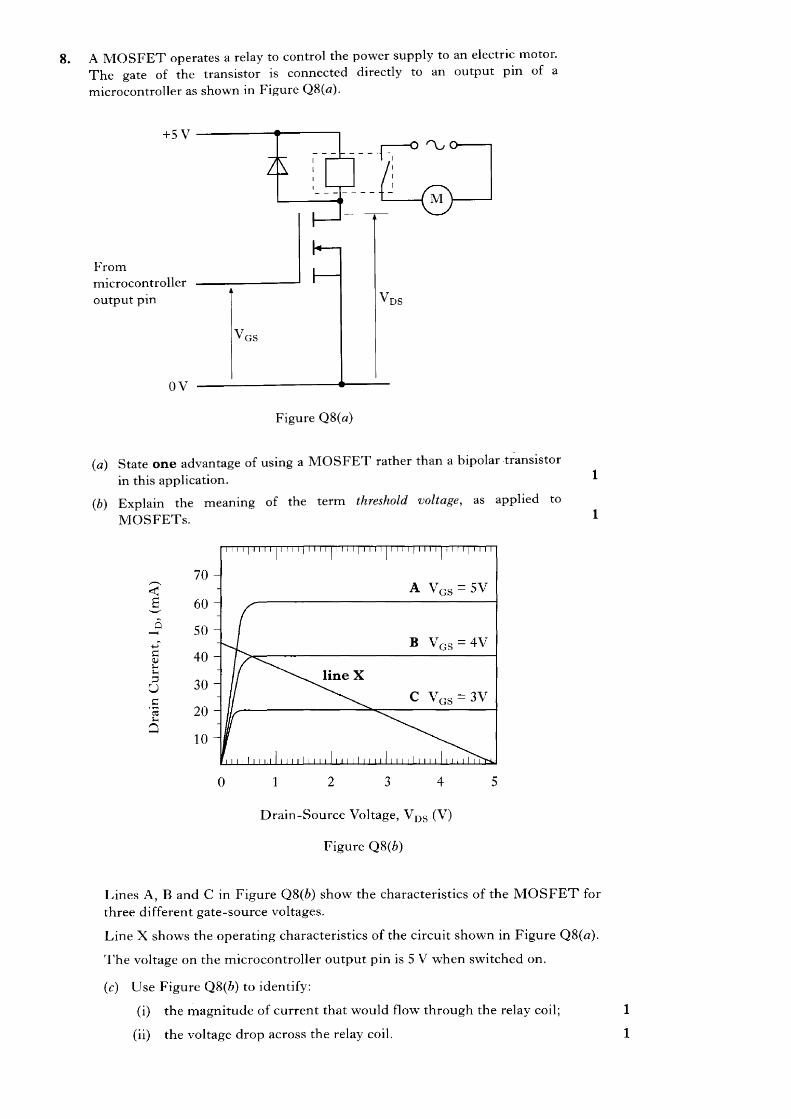
2013 Q8 Higher A car is fitted with a two-speed heater fan. The power to the heater-fan motor is controlled by a single pin from a microcontroller. Assuming no losses in the output driver, the heater-fan motor receives either 100% or 60% of the full power available. (a) State the full name of the technique used to vary the power to an output device using a single pin of a microcontroller. (b) Draw a clearly labelled graph, showing how this technique could be used to control the heater-fan motor so that it runs at 60% of its full power. A MOSFET output-driver circuit provides current to the heater-fan motor. (c) Draw the output-driver circuit showing connections to the motor, the power-supply rails, and to the output pin of the microcontroller.
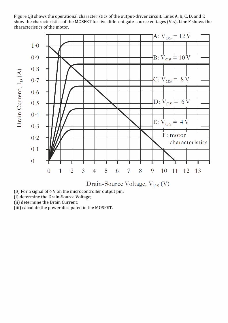
Figure Q8 shows the operational characteristics of the output-driver circuit. Lines A, B, C, D, and E show the characteristics of the MOSFET for five different gate-source voltages (VGS). Line F shows the characteristics of the motor.
(d) For a signal of 4 V on the microcontroller output pin: (i) determine the Drain-Source Voltage; (ii) determine the Drain Current; (iii) calculate the power dissipated in the MOSFET.
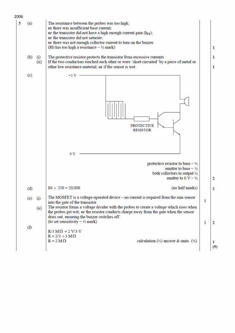
2006
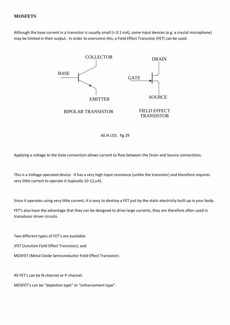
MOSFETS
Although the base current in a transistor is usually small (< 0.1 mA), some input devices (e.g. a crystal microphone)
may be limited in their output. In order to overcome this, a Field Effect Transistor (FET) can be used.
COLLECTOR
EMITTER
BASE
DRAIN
SOURCE
GATE
BIPOLAR TRANSISTOR FIELD EFFECTTRANSISTOR
AE.H.LO1. fig 29
Applying a voltage to the Gate connection allows current to flow between the Drain and Source connections.
This is a Voltage operated device. It has a very high input resistance (unlike the transistor) and therefore requires
very little current to operate it (typically 10-12 A).
Since it operates using very little current, it is easy to destroy a FET just by the static electricity built up in your body.
FET’s also have the advantage that they can be designed to drive large currents, they are therefore often used in
transducer driver circuits.
Two different types of FET’s are available:
JFET (Junction Field Effect Transistor); and
MOSFET (Metal Oxide Semiconductor Field Effect Transistor).
All FET’s can be N-channel or P-channel.
MOSFET’s can be “depletion type” or “enhancement type”.
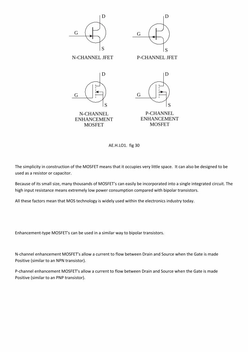
G
GG
G
D
DD
D
S
SS
S
N-CHANNEL JFET P-CHANNEL JFET
N-CHANNELENHANCEMENT
MOSFET
P-CHANNELENHANCEMENT
MOSFET
AE.H.LO1. fig 30
The simplicity in construction of the MOSFET means that it occupies very little space. It can also be designed to be
used as a resistor or capacitor.
Because of its small size, many thousands of MOSFET’s can easily be incorporated into a single integrated circuit. The
high input resistance means extremely low power consumption compared with bipolar transistors.
All these factors mean that MOS technology is widely used within the electronics industry today.
Enhancement-type MOSFET's can be used in a similar way to bipolar transistors.
N-channel enhancement MOSFET’s allow a current to flow between Drain and Source when the Gate is made
Positive (similar to an NPN transistor).
P-channel enhancement MOSFET’s allow a current to flow between Drain and Source when the Gate is made
Positive (similar to an PNP transistor).
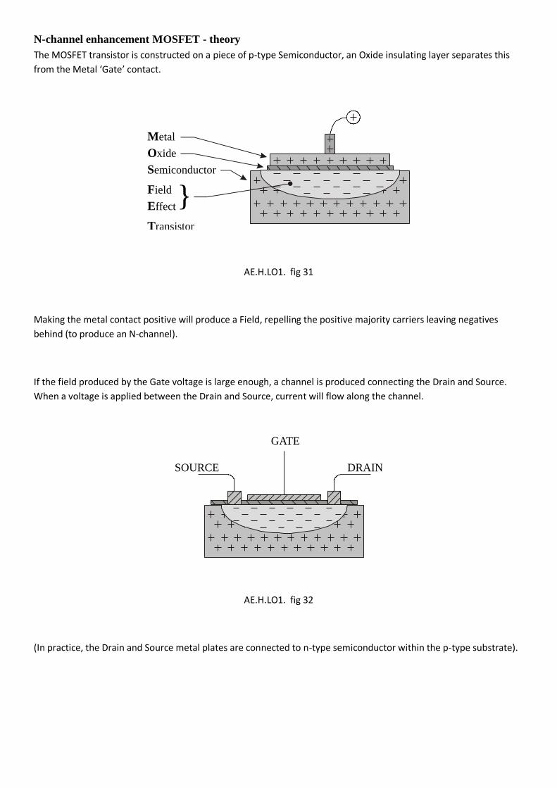
N-channel enhancement MOSFET - theory
The MOSFET transistor is constructed on a piece of p-type Semiconductor, an Oxide insulating layer separates this
from the Metal ‘Gate’ contact.
AE.H.LO1. fig 31
Making the metal contact positive will produce a Field, repelling the positive majority carriers leaving negatives
behind (to produce an N-channel).
If the field produced by the Gate voltage is large enough, a channel is produced connecting the Drain and Source.
When a voltage is applied between the Drain and Source, current will flow along the channel.
AE.H.LO1. fig 32
(In practice, the Drain and Source metal plates are connected to n-type semiconductor within the p-type substrate).
Metal
Oxide
Semiconductor
Field
Effect
Transistor
}
SOURCE
GATE
DRAIN
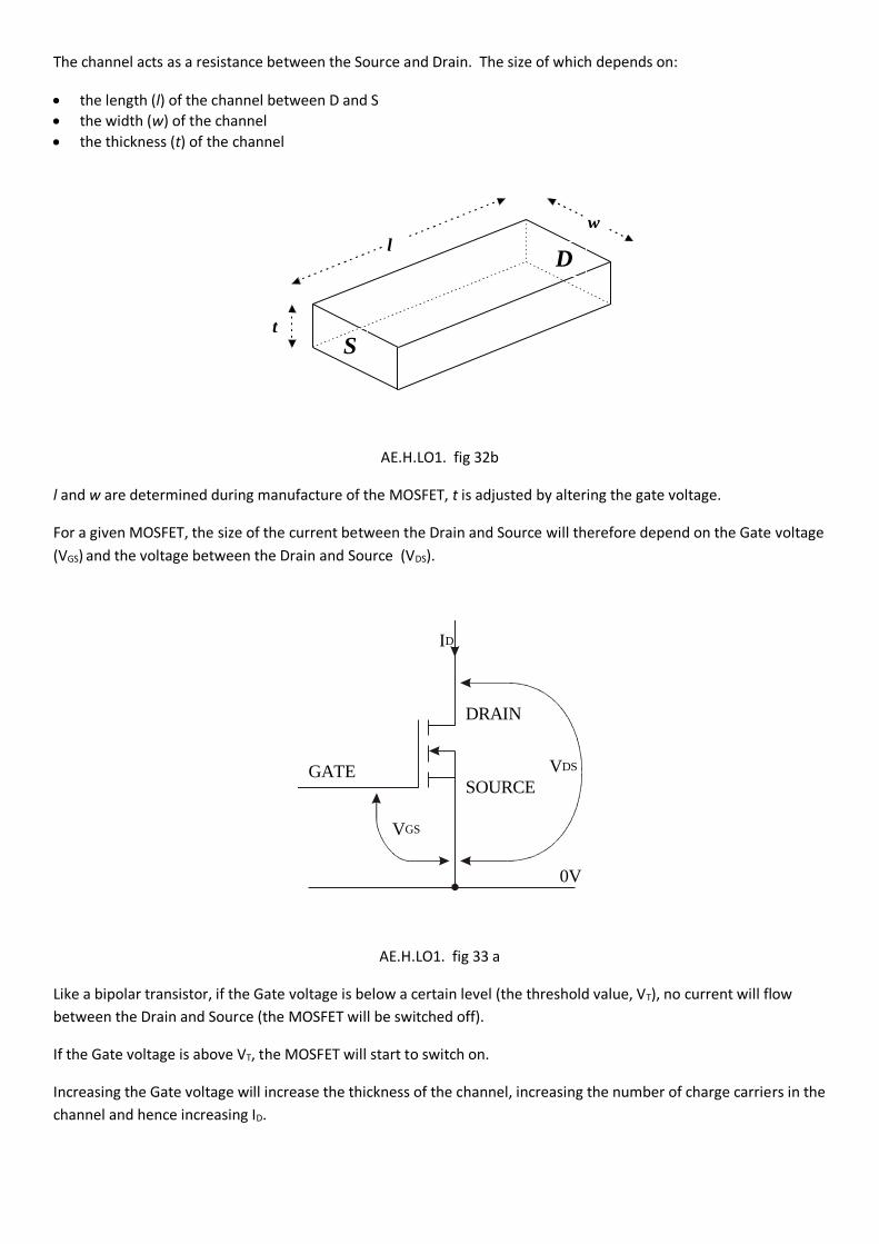
The channel acts as a resistance between the Source and Drain. The size of which depends on:
• the length (l) of the channel between D and S
• the width (w) of the channel
• the thickness (t) of the channel
w
l
t
S
D
AE.H.LO1. fig 32b
l and w are determined during manufacture of the MOSFET, t is adjusted by altering the gate voltage.
For a given MOSFET, the size of the current between the Drain and Source will therefore depend on the Gate voltage
(VGS) and the voltage between the Drain and Source (VDS).
GATE
DRAIN
SOURCE
ID
VGS
VDS
0V
AE.H.LO1. fig 33 a
Like a bipolar transistor, if the Gate voltage is below a certain level (the threshold value, VT), no current will flow
between the Drain and Source (the MOSFET will be switched off).
If the Gate voltage is above VT, the MOSFET will start to switch on.
Increasing the Gate voltage will increase the thickness of the channel, increasing the number of charge carriers in the
channel and hence increasing ID.
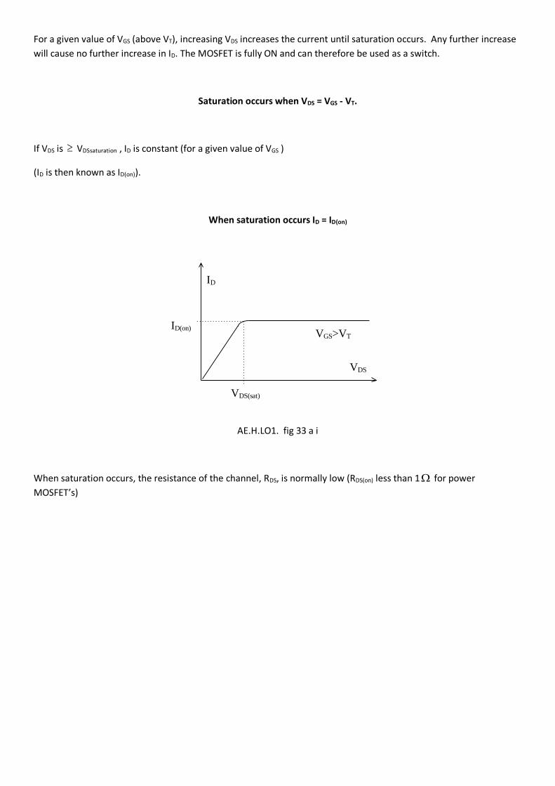
For a given value of VGS (above VT), increasing VDS increases the current until saturation occurs. Any further increase
will cause no further increase in ID. The MOSFET is fully ON and can therefore be used as a switch.
Saturation occurs when VDS = VGS - VT.
If VDS is VDSsaturation , ID is constant (for a given value of VGS )
(ID is then known as ID(on)).
When saturation occurs ID = ID(on)
ID(on)
VDS(sat)
VGS>VT
VDS
ID
AE.H.LO1. fig 33 a i
When saturation occurs, the resistance of the channel, RDS, is normally low (RDS(on) less than 1 for power
MOSFET’s)
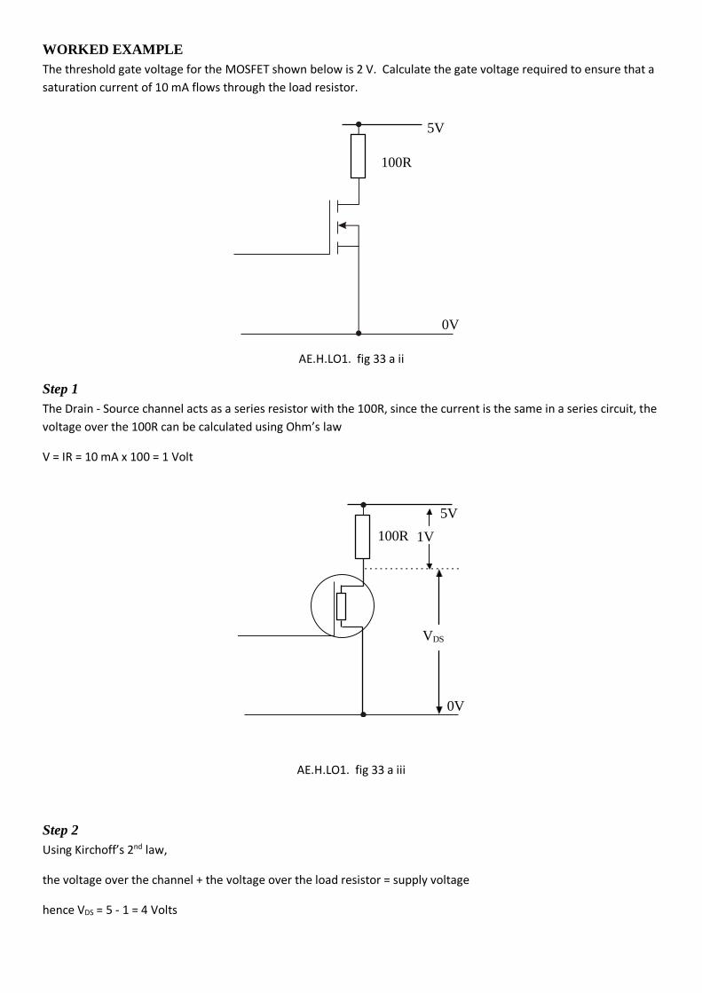
WORKED EXAMPLE
The threshold gate voltage for the MOSFET shown below is 2 V. Calculate the gate voltage required to ensure that a
saturation current of 10 mA flows through the load resistor.
0V
5V
100R
AE.H.LO1. fig 33 a ii
Step 1
The Drain - Source channel acts as a series resistor with the 100R, since the current is the same in a series circuit, the
voltage over the 100R can be calculated using Ohm’s law
V = IR = 10 mA x 100 = 1 Volt
0V
5V
100R 1V
VDS
AE.H.LO1. fig 33 a iii
Step 2
Using Kirchoff’s 2nd law,
the voltage over the channel + the voltage over the load resistor = supply voltage
hence VDS = 5 - 1 = 4 Volts
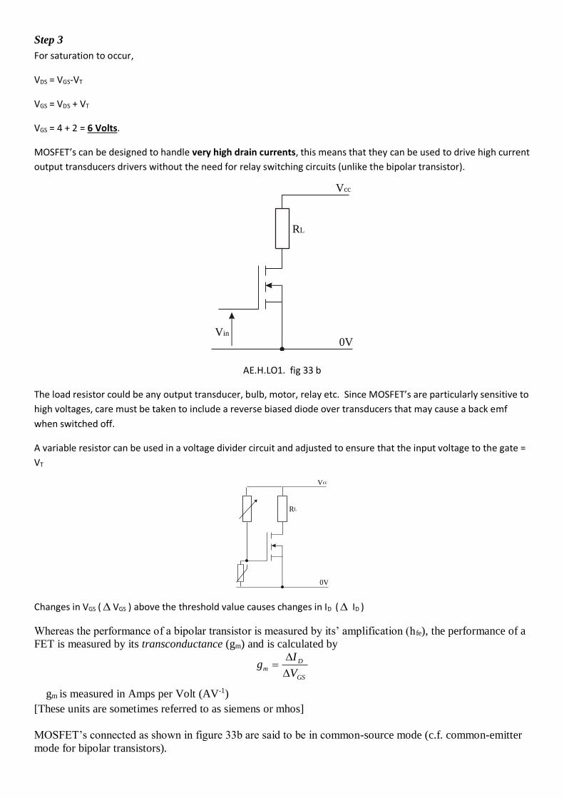
Step 3
For saturation to occur,
VDS = VGS-VT
VGS = VDS + VT
VGS = 4 + 2 = 6 Volts.
MOSFET’s can be designed to handle very high drain currents, this means that they can be used to drive high current
output transducers drivers without the need for relay switching circuits (unlike the bipolar transistor).
AE.H.LO1. fig 33 b
The load resistor could be any output transducer, bulb, motor, relay etc. Since MOSFET’s are particularly sensitive to
high voltages, care must be taken to include a reverse biased diode over transducers that may cause a back emf
when switched off.
A variable resistor can be used in a voltage divider circuit and adjusted to ensure that the input voltage to the gate =
VT
0V
RL
Vcc
Changes in VGS ( VGS ) above the threshold value causes changes in ID ( ID )
Whereas the performance of a bipolar transistor is measured by its’ amplification (hfe), the performance of a
FET is measured by its transconductance (gm) and is calculated by
gI
Vm
D
GS
gm is measured in Amps per Volt (AV-1)
[These units are sometimes referred to as siemens or mhos]
MOSFET’s connected as shown in figure 33b are said to be in common-source mode (c.f. common-emitter
mode for bipolar transistors).
0V
RL
Vcc
Vin
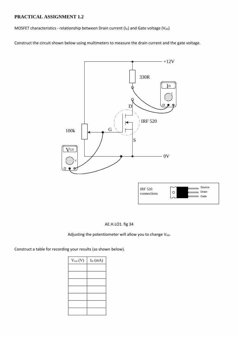
PRACTICAL ASSIGNMENT 1.2
MOSFET characteristics - relationship between Drain current (ID) and Gate voltage (VGS)
Construct the circuit shown below using multimeters to measure the drain current and the gate voltage.
0V
+12V
I
ID
V
VGS
G
D
S
IRF 520
330R
100k
Drain
Gate
SourceIRF 520
connections
AE.H.LO1. fig 34
Adjusting the potentiometer will allow you to change VGS.
Construct a table for recording your results (as shown below).
VGS (V) ID (mA)
Measure ID for various values of VGS.
Find the threshold voltage for this MOSFET
Plot a graph of ID against VGS and calculate gm for this MOSFET.
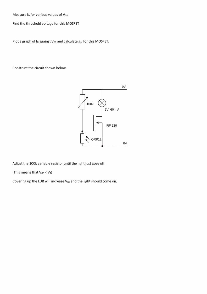
Construct the circuit shown below.
ORP12
0V
6V, 60 mA
9V
100k
IRF 520
Adjust the 100k variable resistor until the light just goes off.
(This means that VGS < VT)
Covering up the LDR will increase VGS and the light should come on.


![Vth Instability of MOSFETs with Advanced Gate Dielectrics [phD thesis]](https://img.pdfslide.us/doc/110x75/5571f2ed49795947648d4256/vth-instability-of-mosfets-with-advanced-gate-dielectrics-phd-thesis.jpg)