Embed Size (px)
Citation preview

Topic 2 :16 Bit Microprocessor: 8086 (24 Marks)
Features of 8086
8086 is a 16 bit processor. It’s ALU, internal registers works with 16bit binary word
8086 has a 16bit data bus. It can read or write data to a memory/port either 16bits or 8 bit at a
time 8086 has a 20bit address bus which means, it can address upto 2^20 = 1MB memory
location Frequency range of 8086 is 6-10 MHz
Introduction to 16-bit Microprocessor: The 16-bit Microprocessor families are designed primarily to complete with
microcomputers and are oriented towards high-level languages. Their applications sometimes overlap those of the 8-bit microprocessors. The have powerful instruction sets and capable of addressing mega bytes of memory.
The era of 16-bit Microprocessors began in 1974 with the introduction of PACE chip by National Semiconductor. The Texas Instruments TMS9900 was introduced in the year 1976. The Intel 8086 commercially available in the year 1978, Zilog Z800 in the year 1979, The Motorola MC68000 in the year 1980.
The 16-bit Microprocessors are available in different pin packages.
Ex: Intel 8086/8088 40 pin package
Zilog Z8001 40 pin package
Digital equipment LSI-II 40 pin package
Motorola MC68000 64 pin package
National Semiconductor NS16000 48 pin package
The primary objectives of this 16-bit Microprocessor can be summarized as follows.
1. Increase memory addressing capability
2. Increase execution speed
3. Provide a powerful instruction set
Facilitate programming in high-level languages.
The INTEL iAPX 8086/8088: It is a 16-bit Microprocessor housed in a 40-pin Dual-Inline-Package (DIP) and capable
of addressing 1Megabyte of memory, various versions of this chip can operate with different clock frequencies
i. 8086 (5 MHz) ii.8086-2 (8 MHz) iii. 8086-1 (10 MHz).
It contains approximately 29,000 transistors and is fabricated using the HMOS technology . The term 16-bit means that its arithmetic logic unit, its internal registers and most of its instructions are designed to work with 16-bit binary word. The 8086 Microprocessor has a 16-bit data bus, so it can read from or write data to memory and ports either 16-bits or 8-bits at a time. The 8086 Microprocessor has 20-bit address bus, so it can address any one of 220 or 1,048,576 memory locations. Here 16-bit words will be stored in two consecutive memory locations. If the first byte of a word is at an even address, the 8086 can read entire word in one operation, If the first byte of the word is at an odd address the 8086 will read the first byte with one bus operation and the

second byte with another bus operation
Architecture: The internal architecture 8086 microprocessor is as shown in the fig 1.2.The 8086 CPU is
divided into two independent functional parts, the Bus interface unit (BIU) and execution unit (EU).
The Bus Interface Unit contains Bus Interface Logic, Segment registers, Memory addressing logic and a Six byte instruction object code queue. The execution unit contains the Data and Address registers, the Arithmetic and Logic Unit, the Control Unit and flags. Draw architecture of 8086 and label it. Write the function of BIU and EU. ( Diagram :4 Marks; Any TWO functions of each unit : 2Marks)
Fig1.2. Internal architecture of 8086 Microprocessor
FUNCTIONS OF EXECUTION UNIT: 1.To tell BIU to fetch the instructions or data from
memory 2.To decode the instructions.
3.To generate different internal and external
controls signal. 4.To execute the instructions.
5.To perform Arithmetic and Logic Operations
FUNCTIONS OF BUS INTERFACE UNIT:
1.Communication with External devices and peripheral including memory
via bus. 2.Fetch the instruction or data from memory.
3.Read data from the port.
4.Write the data to memory and port.
5.Calculation of physical address for accessing the data to and from memory
Memory
Program, data and stack memories occupy the same memory space. The total addressable
memory size is 1MB KB. As the most of the processor instructions use 16-bit pointers the
processor can effectively address only 64 KB of memory. To access memory outside of 64 KB
the CPU uses special segment registers to specify where the code, stack and data 64 KB
segments are positioned within 1 MB of memory (see the "Registers" section below).
16-bit pointers and data are stored as:
address: low-order byte
address+1: high-order byte
32-bit addresses are stored in "segment:offset" format as:
address: low-order byte of segment
address+1: high-order byte of segment
address+2: low-order byte of offset
address+3: high-order byte of offset
Physical memory address pointed by segment:offset pair is calculated as:
address = (<segment> * 16) + <offset>
Program memory - program can be located anywhere in memory. Jump and call instructions
can be used for short jumps within currently selected 64 KB code segment, as well as for far
jumps anywhere within 1 MB of memory. All conditional jump instructions can be used to jump
within approximately +127 - -127 bytes from current instruction.
Data memory - the 8086 processor can access data in any one out of 4 available segments,
which limits the size of accessible memory to 256 KB (if all four segments point to different 64
KB blocks). Accessing data from the Data, Code, Stack or Extra segments can be usually done
by prefixing instructions with the DS:, CS:, SS: or ES: (some registers and instructions by
default may use the ES or SS segments instead of DS segment).
Word data can be located at odd or even byte boundaries. The processor uses two memory
accesses to read 16-bit word located at odd byte boundaries. Reading word data from even byte
boundaries requires only one memory access.
Stack memory can be placed anywhere in memory. The stack can be located at odd memory
addresses, but it is not recommended for performance reasons (see "Data Memory" above).
Reserved locations:
0000h - 03FFh are reserved for interrupt vectors. Each interrupt vector is a 32-bit pointer
in format segment:offset.
FFFF0h - FFFFFh - after RESET the processor always starts program execution at the
FFFF0h address.
Interrupts
The processor has the following interrupts:
INTR is a maskable hardware interrupt. The interrupt can be enabled/disabled using STI/CLI
instructions or using more complicated method of updating the FLAGS register with the help of
the POPF instruction. When an interrupt occurs, the processor stores FLAGS register into stack,
disables further interrupts, fetches from the bus one byte representing interrupt type, and jumps
to interrupt processing routine address of which is stored in location 4 * <interrupt type>.
Interrupt processing routine should return with the IRET instruction.
NMI is a non-maskable interrupt. Interrupt is processed in the same way as the INTR interrupt.
Interrupt type of the NMI is 2, i.e. the address of the NMI processing routine is stored in location
0008h. This interrupt has higher priority then the maskable interrupt.
Software interrupts can be caused by:
INT instruction - breakpoint interrupt. This is a type 3 interrupt.
INT <interrupt number> instruction - any one interrupt from available 256 interrupts.
INTO instruction - interrupt on overflow
Single-step interrupt - generated if the TF flag is set. This is a type 1 interrupt. When the
CPU processes this interrupt it clears TF flag before calling the interrupt processing
routine.
Processor exceptions: divide error (type 0), unused opcode (type 6) and escape opcode
(type 7).
Software interrupt processing is the same as for the hardware interrupts.
I/O ports
65536 8-bit I/O ports. These ports can be also addressed as 32768 16-bit I/O ports.
Registers
Most of the registers contain data/instruction offsets within 64 KB memory segment. There are
four different 64 KB segments for instructions, stack, data and extra data. To specify where in 1

MB of processor memory these 4 segments are located the 8086 microprocessor uses four
segment registers:
Code segment (CS) is a 16-bit register containing address of 64 KB segment with processor
instructions. The processor uses CS segment for all accesses to instructions referenced by
instruction pointer (IP) register. CS register cannot be changed directly. The CS register is
automatically updated during far jump, far call and far return instructions.
Stack segment (SS) is a 16-bit register containing address of 64KB segment with program stack.
By default, the processor assumes that all data referenced by the stack pointer (SP) and base
pointer (BP) registers is located in the stack segment. SS register can be changed directly using
POP instruction.
Data segment (DS) is a 16-bit register containing address of 64KB segment with program data.
By default, the processor assumes that all data referenced by general registers (AX, BX, CX,
DX) and index register (SI, DI) is located in the data segment. DS register can be changed
directly using POP and LDS instructions.
Extra segment (ES) is a 16-bit register containing address of 64KB segment, usually with
program data. By default, the processor assumes that the DI register references the ES segment
in string manipulation instructions. ES register can be changed directly using POP and LES
instructions.
It is possible to change default segments used by general and index registers by prefixing
instructions with a CS, SS, DS or ES prefix.
All general registers of the 8086 microprocessor can be used for arithmetic and logic operations.
The general registers are:
Accumulator register consists of 2 8-bit registers AL and AH, which can be combined together
and used as a 16-bit register AX. AL in this case contains the low-order byte of the word, and
AH contains the high-order byte. Accumulator can be used for I/O operations and string
manipulation.
Base register consists of 2 8-bit registers BL and BH, which can be combined together and used
as a 16-bit register BX. BL in this case contains the low-order byte of the word, and BH contains
the high-order byte. BX register usually contains a data pointer used for based, based indexed or
register indirect addressing.
Count register consists of 2 8-bit registers CL and CH, which can be combined together and
used as a 16-bit register CX. When combined, CL register contains the low-order byte of the
word, and CH contains the high-order byte. Count register can be used as a counter in string
manipulation and shift/rotate instructions.
Data register consists of 2 8-bit registers DL and DH, which can be combined together and used
as a 16-bit register DX. When combined, DL register contains the low-order byte of the word,

and DH contains the high-order byte. Data register can be used as a port number in I/O
operations. In integer 32-bit multiply and divide instruction the DX register contains high-order
word of the initial or resulting number.
The following registers are both general and index registers:
Stack Pointer (SP) is a 16-bit register pointing to program stack.
Base Pointer (BP) is a 16-bit register pointing to data in stack segment. BP register is usually
used for based, based indexed or register indirect addressing.
Source Index (SI) is a 16-bit register. SI is used for indexed, based indexed and register indirect
addressing, as well as a source data address in string manipulation instructions.
Destination Index (DI) is a 16-bit register. DI is used for indexed, based indexed and register
indirect addressing, as well as a destination data address in string manipulation instructions.
Other registers:
Instruction Pointer (IP) is a 16-bit register.
Flags is a 16-bit register containing 9 1-bit flags:
Overflow Flag (OF) - set if the result is too large positive number, or is too small
negative number to fit into destination operand.
Direction Flag (DF) - if set then string manipulation instructions will auto-decrement
index registers. If cleared then the index registers will be auto-incremented.
Interrupt-enable Flag (IF) - setting this bit enables maskable interrupts.
Single-step Flag (TF) - if set then single-step interrupt will occur after the next
instruction.
Sign Flag (SF) - set if the most significant bit of the result is set.
Zero Flag (ZF) - set if the result is zero.
Auxiliary carry Flag (AF) - set if there was a carry from or borrow to bits 0-3 in the AL
register.
Parity Flag (PF) - set if parity (the number of "1" bits) in the low-order byte of the result
is even.
Carry Flag (CF) - set if there was a carry from or borrow to the most significant bit
during last result calculation.
Instruction Set
Instruction set of Intel 8086 processor consists of the following instructions:
Data moving instructions.
Arithmetic - add, subtract, increment, decrement, convert byte/word and compare.
Logic - AND, OR, exclusive OR, shift/rotate and test.
String manipulation - load, store, move, compare and scan for byte/word.
Control transfer - conditional, unconditional, call subroutine and return from subroutine.
Input/Output instructions.
Other - setting/clearing flag bits, stack operations, software interrupts, etc.
Addressing modes
Implied - the data value/data address is implicitly associated with the instruction.
Register - references the data in a register or in a register pair.
Immediate - the data is provided in the instruction.
Direct - the instruction operand specifies the memory address where data is located.
Register indirect - instruction specifies a register containing an address, where data is located.
This addressing mode works with SI, DI, BX and BP registers.
Based - 8-bit or 16-bit instruction operand is added to the contents of a base register (BX or BP),
the resulting value is a pointer to location where data resides.
Indexed - 8-bit or 16-bit instruction operand is added to the contents of an index register (SI or
DI), the resulting value is a pointer to location where data resides.
Based Indexed - the contents of a base register (BX or BP) is added to the contents of an index
register (SI or DI), the resulting value is a pointer to location where data resides.
Based Indexed with displacement - 8-bit or 16-bit instruction operand is added to the contents
of a base register (BX or BP) and index register (SI or DI), the resulting value is a pointer to
location where data resides.
Working The BIU sends out address, fetches the instructions from memory, read data from ports
and memory, and writes the data to ports and memory. In other words the BIU handles all transfers of data and addresses on the buses for the execution unit.
The execution unit (EU) of the 8086 tells the BIU where to fetch instructions or data from, decodes instructions and executes instruction. The EU contains control circuitry which directs internal operations. A decoder in the EU translates instructions fetched from memory into a series of actions which the EU carries out. The EU is has a 16-bit ALU which can add, subtract, AND, OR, XOR, increment, decrement, complement or shift binary numbers. The EU is decoding an instruction or executing an instruction which does not require use of the buses.
The Queue: The BIU fetches up to 6 instruction bytes for the following instructions. The BIU stores these prefetched bytes in first-in-first-out register set called a queue. When the EU is ready for its next instruction it simply reads the instruction byte(s) for the instruction from the queue in
the BIU. This is much faster than sending out an address to the system memory and waiting for memory to send back the next instruction byte or bytes. Except in the case of JMP and CALL instructions, where the queue must be dumped and then reloaded starting from a new address, this prefetch-and-queue scheme greatly speeds up processing. Fetching the next instruction while the current instruction executes is called pipelining.
Word Read Each of 1 MB memory address of 8086 represents a byte wide location.16-bit words will
be stored in two consecutive memory locations. If first byte of the data is stored at an even address, 8086 can read the entire word in one operation.
For example if the 16 bit data is stored at even address 00520H is 9634H MOV BX, [00520H]
8086 reads the first byte and stores the data in BL and reads the 2nd
byte and stores the data in BH
BL= (00520H) i.e.BL=34H
BH= (00521H) BH=96H If the first byte of the data is stored at an odd address, 8086 needs two operations to read the 16 bit data.
For example if the 16 bit data is stored at even address 00521H is 3897H MOV BX, [00521H]
In first operation, 8086 reads the 16 bit data from the 00520H location and stores the data of 00521H location in register BL and discards the data of 00520H location In 2
nd operation, 8086
reads the 16 bit data from the 00522H location and stores the data of 00522H location in register BH and discards the data of 00523H location.
BL= (00521H) i.e. BL=97H
BH= (00522H) BH=38H
Byte Read:
MOV BH, [Addr] For Even Address:
Ex: MOV BH, [00520H] 8086 reads the first byte from 00520 location and stores the data in BH and reads the 2
nd byte
from the 00521H location and ignores it BH =[ 00520H]
For Odd Address MOV BH, [Addr]
Ex: MOV BH, [00521H] 8086 reads the first byte from 00520H location and ignores it and reads the 2nd byte from the 00521 location and stores the data in BH
BH = [00521H]
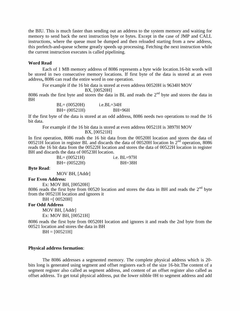
Physical address formation:
The 8086 addresses a segmented memory. The complete physical address which is 20-bits long is generated using segment and offset registers each of the size 16-bit.The content of a segment register also called as segment address, and content of an offset register also called as offset address. To get total physical address, put the lower nibble 0H to segment address and add
offset address. The fig 1.3 shows formation of 20-bit physical address.
Fig. 1.3. Physical address formation
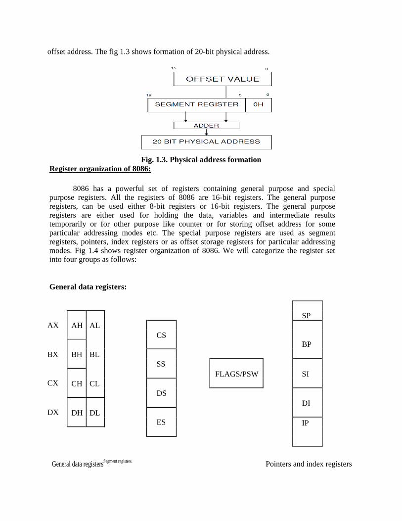
Register organization of 8086:
8086 has a powerful set of registers containing general purpose and special purpose registers. All the registers of 8086 are 16-bit registers. The general purpose registers, can be used either 8-bit registers or 16-bit registers. The general purpose registers are either used for holding the data, variables and intermediate results temporarily or for other purpose like counter or for storing offset address for some particular addressing modes etc. The special purpose registers are used as segment registers, pointers, index registers or as offset storage registers for particular addressing modes. Fig 1.4 shows register organization of 8086. We will categorize the register set into four groups as follows:
General data registers:
AX
SP
AH AL
CS
BP
BX BH BL
SS
CX
FLAGS/PSW
SI
CH CL
DS
DX
DI
DH DL
ES
IP
General data registersSegment registers
Pointers and index registers

Fig.1.4 Register organization of 8086 Microprocessor
The registers AX, BX, CX, and DX are the general 16-bit registers.
AX Register: Accumulator register consists of two 8-bit registers AL and AH, which can be combined together and used as a 16- bit register AX. AL in this case contains the low-order byte of the word, and AH contains the high-order byte. Accumulator can be used for I/O operations, rotate and string manipulation.
BX Register: This register is mainly used as a base register. It holds the starting base location of a memory region within a data segment. It is used as offset storage for forming physical address in case of certain addressing mode.
CX Register: It is used as default counter or count register in case of string and loop instructions.
DX Register: Data register can be used as a port number in I/O operations and implicit operand or destination in case of few instructions. In integer 32-bit multiply and divide instruction the DX register contains high-order word of the initial or resulting number.
Segment registers: To complete 1Mbyte memory is divided into 16 logical segments. The complete 1Mbyte
memory segmentation is as shown in fig 1.5. Each segment contains 64Kbyte of memory. There are four segment registers.
Code segment (CS) is a 16-bit register containing address of 64 KB segment with processor instructions. The processor uses CS segment for all accesses to instructions referenced by instruction pointer (IP) register. CS register cannot be changed directly. The CS register is automatically updated during far jump, far call and far return instructions. It is used for addressing a memory location in the code segment of the memory, where the executable program is stored.
Stack segment (SS) is a 16-bit register containing address of 64KB segment with program stack. By default, the processor assumes that all data referenced by the stack pointer (SP) and base pointer (BP) registers is located in the stack segment. SS register can be changed directly using POP instruction. It is used for addressing stack segment of memory. The stack segment is that segment of memory, which is used to store stack data.
Data segment (DS) is a 16-bit register containing address of 64KB segment with program data. By default, the processor assumes that all data referenced by general registers (AX, BX, CX, DX) and index register (SI, DI) is located in the data segment. DS register can be changed directly using POP and LDS instructions. It points to the data segment memory where the data is resided.
Extra segment (ES) is a 16-bit register containing address of 64KB segment, usually with

program data. By default, the processor assumes that the DI register references the ES segment in string manipulation instructions. ES register can be changed directly using POP and LES instructions. It also refers to segment which essentially is another data segment of the memory. It also contains data.
Fig1.5. Memory segmentation
Pointers and index registers. The pointers contain within the particular segments. The pointers IP, BP, SP usually
contain offsets within the code, data and stack segments respectively
Stack Pointer (SP) is a 16-bit register pointing to program stack in stack segment.
Base Pointer (BP) is a 16-bit register pointing to data in stack segment. BP register is usually used for based, based indexed or register indirect addressing.
Source Index (SI) is a 16-bit register. SI is used for indexed, based indexed and register indirect addressing, as well as a source data addresses in string manipulation instructions.
Destination Index (DI) is a 16-bit register. DI is used for indexed, based indexed and register indirect addressing, as well as a destination data address in string manipulation instructions.
Flag register
15 14 13 12 11 10 9 8 7 6 5 4 3 2 1 1
X X X X OF DF IF TF SF ZF X AC X PF X CY
X = Undefined
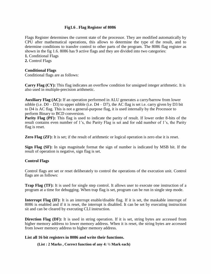
Fig1.6 . Flag Register of 8086
Flags Register determines the current state of the processor. They are modified automatically by CPU after mathematical operations, this allows to determine the type of the result, and to determine conditions to transfer control to other parts of the program. The 8086 flag register as shown in the fig 1.6. 8086 has 9 active flags and they are divided into two categories: 1. Conditional Flags
2. Control Flags
Conditional Flags Conditional flags are as follows:
Carry Flag (CY): This flag indicates an overflow condition for unsigned integer arithmetic. It is also used in multiple-precision arithmetic.
Auxiliary Flag (AC): If an operation performed in ALU generates a carry/barrow from lower nibble (i.e. D0 – D3) to upper nibble (i.e. D4 – D7), the AC flag is set i.e. carry given by D3 bit to D4 is AC flag. This is not a general-purpose flag, it is used internally by the Processor to perform Binary to BCD conversion. Parity Flag (PF): This flag is used to indicate the parity of result. If lower order 8-bits of the result contains even number of 1’s, the Parity Flag is set and for odd number of 1’s, the Parity flag is reset.
Zero Flag (ZF): It is set; if the result of arithmetic or logical operation is zero else it is reset.
Sign Flag (SF): In sign magnitude format the sign of number is indicated by MSB bit. If the result of operation is negative, sign flag is set.
Control Flags
Control flags are set or reset deliberately to control the operations of the execution unit. Control flags are as follows:
Trap Flag (TF): It is used for single step control. It allows user to execute one instruction of a program at a time for debugging. When trap flag is set, program can be run in single step mode.
Interrupt Flag (IF): It is an interrupt enable/disable flag. If it is set, the maskable interrupt of 8086 is enabled and if it is reset, the interrupt is disabled. It can be set by executing instruction sit and can be cleared by executing CLI instruction.
Direction Flag (DF): It is used in string operation. If it is set, string bytes are accessed from higher memory address to lower memory address. When it is reset, the string bytes are accessed from lower memory address to higher memory address.
List all 16 bit registers in 8086 and write their functions.
(List : 2 Marks , Correct function of any 4: ½ Mark each)
Ans: EU contains 8 general purpose registers : AX, BX, CX, DX, SP, BP, SI, DI, DS, CS, SS, ES,IP and flag register.
AX, BX, CX, DX : used as eight 8-bit registers i.e AL, AH, BL, BH, CL, CH, DL, DH or 16-bit register. AL functions as 8-bit accumulator and AX functions as 16-bit accumulator. CX : used as counter register. BX :used as pointer register. DX :used for I/O addressing.
SP , BP : used as pointer register , SP holds 16-bit offset within stack segment and BP contains offset within the data segment
SI, DI : The register SI is used to store the offset of source data in data segment. The register DI is used to store the offset of destination in data or extra segment.
DS, CS, SS and ES : These are used for Data, Code, Stack and Extra Data ( Strings)
respectively. IP: is used as an instruction pointer which holds the address of the next
instruction to be executed by the microprocessor. Flag register is used to hold the status of arithmetic and logic operations along with
control flags.
Signal Description of 8086 Microprocessor
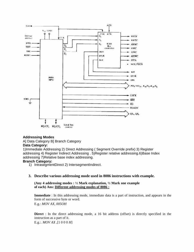
The 8086 Microprocessor is a 16-bit CPU available in 3 clock rates, i.e. 5, 8 and 10MHz, packaged in a 40 pin CERDIP or plastic package. The 8086 Microprocessor operates in single processor or multiprocessor configurations to achieve high performance. The pin configuration is as shown in fig1. Some of the pins serve a particular function in minimum mode (single processor mode) and others function in maximum mode (multiprocessor mode) configuration.
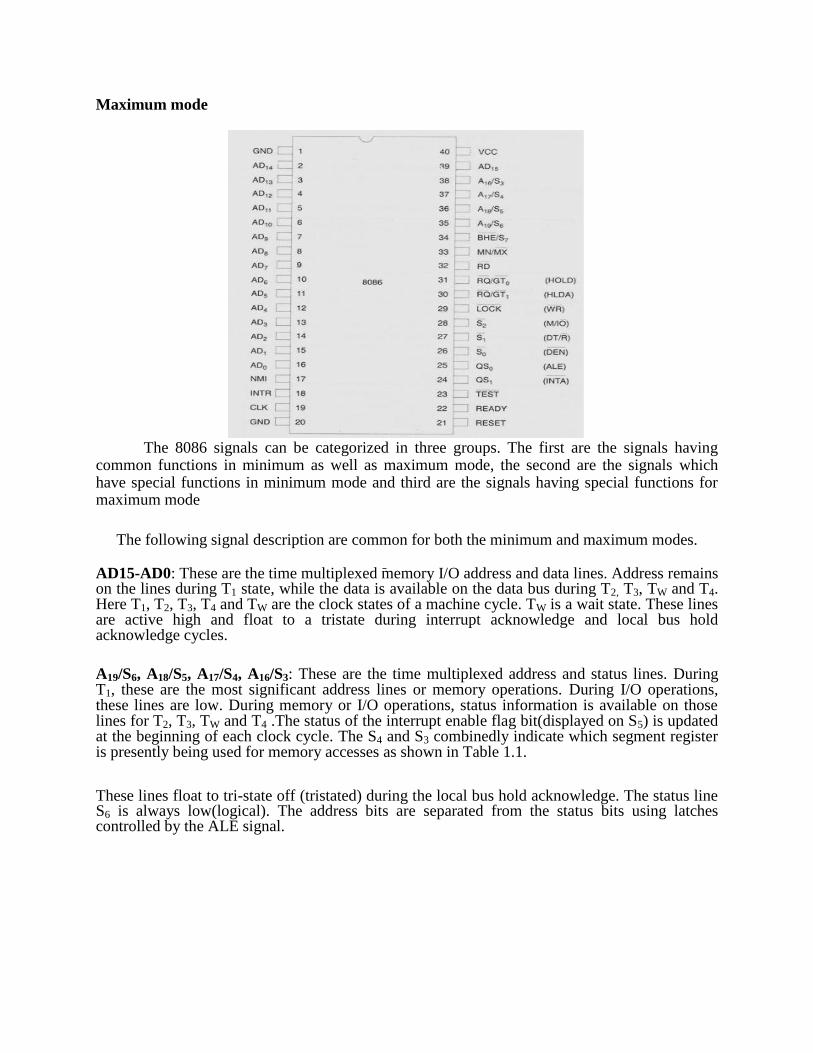
Maximum mode
The 8086 signals can be categorized in three groups. The first are the signals having
common functions in minimum as well as maximum mode, the second are the signals which have special functions in minimum mode and third are the signals having special functions for maximum mode
The following signal description are common for both the minimum and maximum modes.
AD15-AD0: These are the time multiplexed memory I/O address and data lines. Address remains on the lines during T1 state, while the data is available on the data bus during T2, T3, TW and T4. Here T1, T2, T3, T4 and TW are the clock states of a machine cycle. TW is a wait state. These lines are active high and float to a tristate during interrupt acknowledge and local bus hold acknowledge cycles.
A19/S6, A18/S5, A17/S4, A16/S3: These are the time multiplexed address and status lines. During T1, these are the most significant address lines or memory operations. During I/O operations, these lines are low. During memory or I/O operations, status information is available on those lines for T2, T3, TW and T4 .The status of the interrupt enable flag bit(displayed on S5) is updated at the beginning of each clock cycle. The S4 and S3 combinedly indicate which segment register is presently being used for memory accesses as shown in Table 1.1. These lines float to tri-state off (tristated) during the local bus hold acknowledge. The status line S6 is always low(logical). The address bits are separated from the status bits using latches controlled by the ALE signal.
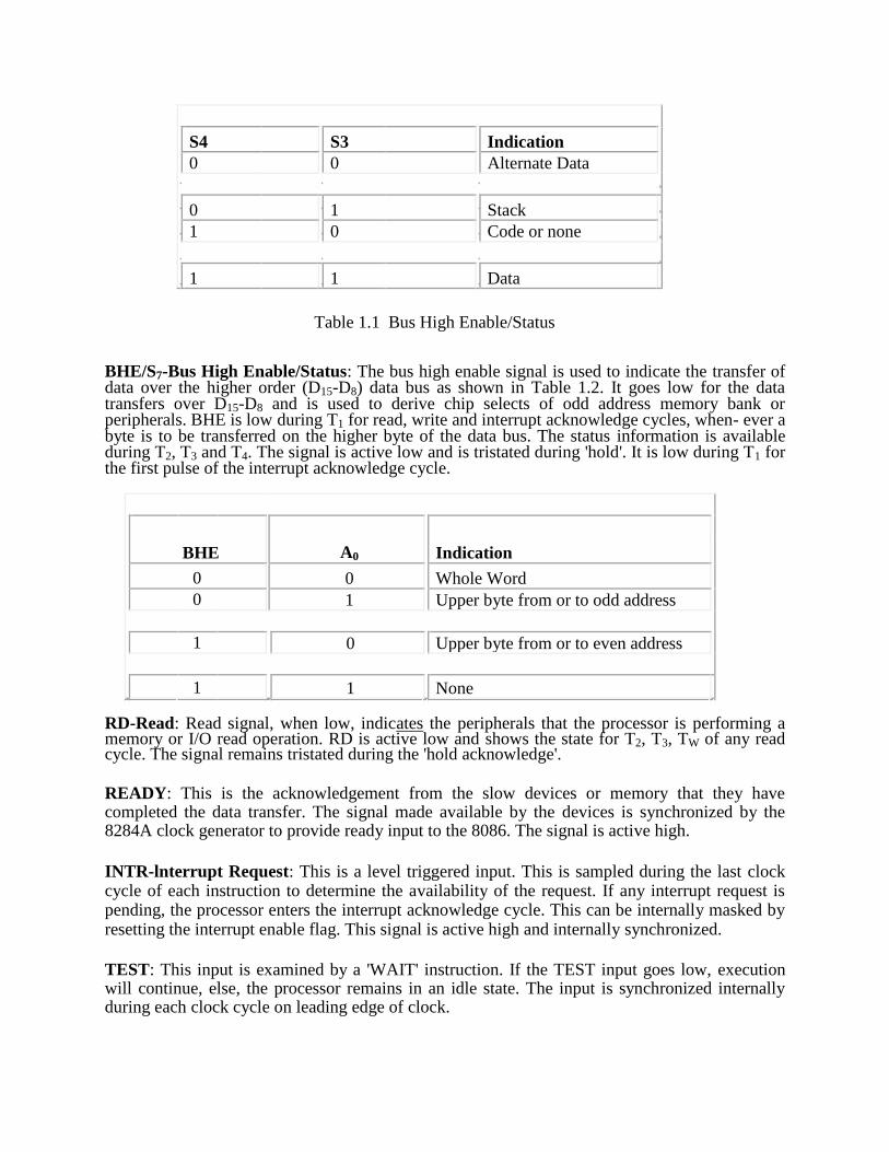
S4 S3 Indication
0 0 Alternate Data
0 1 Stack
1 0 Code or none
1 1 Data
Table 1.1 Bus High Enable/Status BHE/S7-Bus High Enable/Status: The bus high enable signal is used to indicate the transfer of data over the higher order (D15-D8) data bus as shown in Table 1.2. It goes low for the data transfers over D15-D8 and is used to derive chip selects of odd address memory bank or peripherals. BHE is low during T1 for read, write and interrupt acknowledge cycles, when- ever a byte is to be transferred on the higher byte of the data bus. The status information is available during T2, T3 and T4. The signal is active low and is tristated during 'hold'. It is low during T1 for the first pulse of the interrupt acknowledge cycle.
BHE A0 Indication
0 0 Whole Word
0 1 Upper byte from or to odd address
1 0 Upper byte from or to even address
1 1 None RD-Read: Read signal, when low, indicates the peripherals that the processor is performing a memory or I/O read operation. RD is active low and shows the state for T2, T3, TW of any read cycle. The signal remains tristated during the 'hold acknowledge'.
READY: This is the acknowledgement from the slow devices or memory that they have completed the data transfer. The signal made available by the devices is synchronized by the 8284A clock generator to provide ready input to the 8086. The signal is active high.
INTR-lnterrupt Request: This is a level triggered input. This is sampled during the last clock cycle of each instruction to determine the availability of the request. If any interrupt request is pending, the processor enters the interrupt acknowledge cycle. This can be internally masked by resetting the interrupt enable flag. This signal is active high and internally synchronized.
TEST: This input is examined by a 'WAIT' instruction. If the TEST input goes low, execution will continue, else, the processor remains in an idle state. The input is synchronized internally during each clock cycle on leading edge of clock.
NMI-Non-maskable Interrupt: This is an edge-triggered input which causes a Type2 interrrupt. The NMI is not maskable internally by software. A transition from low to high initiates the interrupt response at the end of the current instruction. This input is internally synchronized.
RESET: This input causes the processor to terminate the current activity and start execution from FFFF0H. The signal is active high and must be active for at least four clock cycles. It restarts execution when the RESET returns low. RESET is also internally synchronized.
CLK-Clock Input: The clock input provides the basic timing for processor operation and bus control activity. Its an asymmetric square wave with 33% duty cycle. The range of frequency for different 8086 versions is from 5MHz to 10MHz. VCC : +5V power supply for the operation of the internal circuit. GND ground for the internal circuit.
MN/MX :The logic level at this pin decides whether the processor is to operate in either minimum (single processor) or maximum (multiprocessor) mode. The following pin functions are for the minimum mode operation of 8086. M/IO -Memory/IO: This is a status line logically equivalent to S2 in maximum mode. When it is low, it indicates the CPU is having an I/O operation, and when it is high, it indicates that the CPU is having a memory operation. This line becomes active in the previous T4 and remains active till final T4 of the current cycle. It is tristated during local bus "hold acknowledge”.
INTA -Interrupt Acknowledge: This signal is used as a read strobe for interrupt acknowledge cycles. In other words, when it goes low, it means that the processor has accepted the interrupt. It is active low during T2, T3 and TW of each interrupt acknowledge cycle.
ALE-Address latch Enable: This output signal indicates the availability of the valid address on the address/data lines, and is connected to latch enable input of latches. This signal is active high and is never tristated.
DT /R -Data Transmit/Receive: This output is used to decide the direction of data flow through the transreceivers (bidirectional buffers). When the processor sends out data, this signal is high and when the processor is receiving data, this signal is low. Logically, this is equivalent to S1 in maximum mode. Its timing is the same as M/I/O. This is tristated during 'hold acknowledge'.
DEN-Data Enable This signal indicates the availability of valid data over the address/data lines. It is used to enable the transreceivers (bidirectional buffers) to separate the data from the multiplexed address/data signal. It is active from the middle ofT2 until the middle of T4 DEN is tristated during 'hold acknowledge' cycle.
HOLD, HLDA-Hold/Hold Acknowledge: When the HOLD line goes high, it indicates to the processor that another master is requesting the bus access. The processor, after receiving the HOLD request, issues the hold acknowledge signal on HLDA pin, in the middle of the next clock cycle after completing the current bus (instruction) cycle. At the same time, the processor floats the local bus and control lines. When the processor detects the HOLD line low, it lowers the

HLDA signal. HOLD is an asynchronous input, and it should be externally synchronized.
If the DMA request is made while the CPU is performing a memory or I/O cycle, it will release the local bus during T 4 provided: 1. The request occurs on or before T 2 state of the current cycle.
2. The current cycle is not operating over the lower byte of a word (or operating on an odd address). 3. The current cycle is not the first acknowledge of an interrupt acknowledge sequence. 4. A Lock instruction is not being executed. So far we have presented the pin descriptions of 8086 in minimum mode.
The following pin functions are applicable for maximum mode operation of 8086.
S2, S1, S0 -Status Lines: These are the status lines which reflect the type of operation, being carried out by the processor. These become active during T4 of the previous cycle and remain active during T1 and T2 of the current bus cycle. The status lines return to passive state during T3 of the current bus cycle so that they may again become active for the next bus cycle during T4. Any change in these lines during T3 indicates the starting of a new cycle, and return to passive state indicates end of the bus cycle. These status lines are encoded
S2 S1 S0 Indication
0 0 0 Interrupt Acknowledge
0 0 1 Read I/O Port
0 1 0 Write I/O Port
0 1 1 Halt
1 0 0 Code Access
1 0 1 Read memory
1 1 0 Write memory
1 1 1 Passive
LOCK: This output pin indicates that other system bus masters will be prevented from
gaining the system bus, while the LOCK signal is low. The LOCK signal is activated by the
'LOCK' prefix instruction and remains active until the completion of the next instruction. This floats to tri-state off during "hold acknowledge". When the CPU is executing a critical instruction which requires the system bus, the LOCK prefix instruction ensures that other processors connected in the system will not gain the control of the bus. The 8086, while executing the prefixed instruction, asserts the bus lock signal output, which may be connected to an external bus controller.
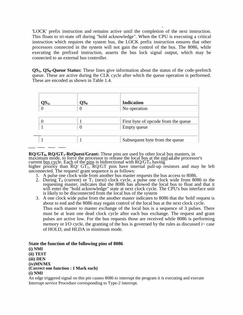
QS1, QS0-Queue Status: These lines give information about the status of the code-prefetch queue. These are active during the CLK cycle after which the queue operation is performed. These are encoded as shown in Table 1.4.
QS1, QS0 Indication
0 0 No operation
0 1 First byte of opcode from the queue
1 0 Empty queue
1 1 Subsequent byte from the queue RQ/GT0, RQ/GT1-ReQuest/Grant: These pins are used by other local bus masters, in maximum mode, to force the processor to release the local bus at the end of the processor's current bus cycle. Each of the pins is bidirectional with RQ/GT0 having higher priority than RQ/ GT1, RQ/GT pins have internal pull-up resistors and may be left unconnected. The request! grant sequence is as follows:
1. A pulse one clock wide from another bus master requests the bus access to 8086. 2. During T4 (current) or T1 (next) clock cycle, a pulse one clock wide from 8086 to the
requesting master, indicates that the 8086 has allowed the local bus to float and that it will enter the "hold acknowledge" state at next clock cycle. The CPU's bus interface unit is likely to be disconnected from the local bus of the system
3. A one clock wide pulse from the another master indicates to 8086 that the 'hold' request is about to end and the 8086 may regain control of the local bus at the next clock cycle. Thus each master to master exchange of the local bus is a sequence of 3 pulses. There must be at least one dead clock cycle after each bus exchange. The request and grant pulses are active low. For the bus requests those are received while 8086 is performing memory or I/O cycle, the granting of the bus is governed by the rules as discussed i~ case of HOLD, and HLDA in minimum mode.
State the function of the following pins of 8086 (i) NMI
(ii) TEST (iii) DEN (iv)MN/MX (Correct one function : 1 Mark each) (i) NMI
An edge triggered signal on this pin causes 8086 to interrupt the program it is executing and execute
Interrupt service Procedure corresponding to Type-2 interrupt.

NMI is Non-maskable by software. ii)TEST – Used to test the status of math co-processor 8087. If signal goes low, execution will continue, else processor remains in an idle state. iii)DEN This is active low signal, to indicate availability of valid data over AD0-AD15.
Used to enable transreceivers(bi-directional buffers) 8286 or 74LS245 to separate data from multiplexed address/data signal . iv)MN/MX This signal indicates operating mode of 8086, minimum or maximum.
When this pin connected to
1) Vcc, the processor operates in minimum mode, 2) Ground , processor operates in maximum mode. 8086-Minimum mode of operation
Minimum Mode Interface Address/Data bus: 20 bits vs 8 bits multiplexed Status signals: A16-A19 multiplexed with status signals S3-S6 respectively.S3 and S4 together form a 2 bit binary code that identifies which of the internal segment registers was used to generate the physical address that was output on the address bus during the current bus cycle. S5 is the logic level of the internal interrupt enable flag, S6 is always logic 0. Control Signals: Address Latch Enable (ALE) is a pulse to logic 1 that signals external circuitry when a valid address is on the bus. This address can be latched in external circuitry on the 1-to-0 edge of the pulse at ALE. IO/M line: memory or I/O transfer is selected (complement for 8086) DT/R line: direction of data is selected SSO (System Status Output) line: =1 when data is read from memory and =0 when code is read from memory (only for 8088) BHE (Bank High Enable) line : =0 for most significant byte of data for 8086 and also carries S7 RD line: =0 when a read cycle is in progress
WR line: =0 when a write cyle is in progress DEN line: (Data enable) Enables the external devices to supply data to the processor. Ready line: can be used to insert wait states into the bus cycle so that it is extended by a number of clock periods Interrupt signals: INTR (Interrupt request) :=1 shows there is a service request, sampled at the final clock cycle of each instruction acquisition cycle. INTA : Processor responds with two pulses going to 0 when it services the interrupt and waits for the interrupt service number after the second pulse. TEST: Processor suspends operation when =1. Resumes operation when=0. Used to syncronize the processor to external events. NMI (Nonmaskable interrupt) : A leading edge transition causes the processor go to the interrupt routine after the current instruction is executed. RESET : =0 Starts the reset sequence. Maximum Mode Interface • For multiprocessor environment • 8288 Bus Controller is used for bus control • WR¯,IO/M¯,DT/R¯,DEN¯,ALE, INTA¯ signals are not available.
o MRDC¯ (memory read command) o MWRT¯ (memory write command) o AMWC¯ (advanced memory write command) o IORC¯ (I/O read command) o IOWC¯ (I/O write command) o AIOWC¯ (Advanced I/O write command) o INTA¯ (interrupt acknowledge)
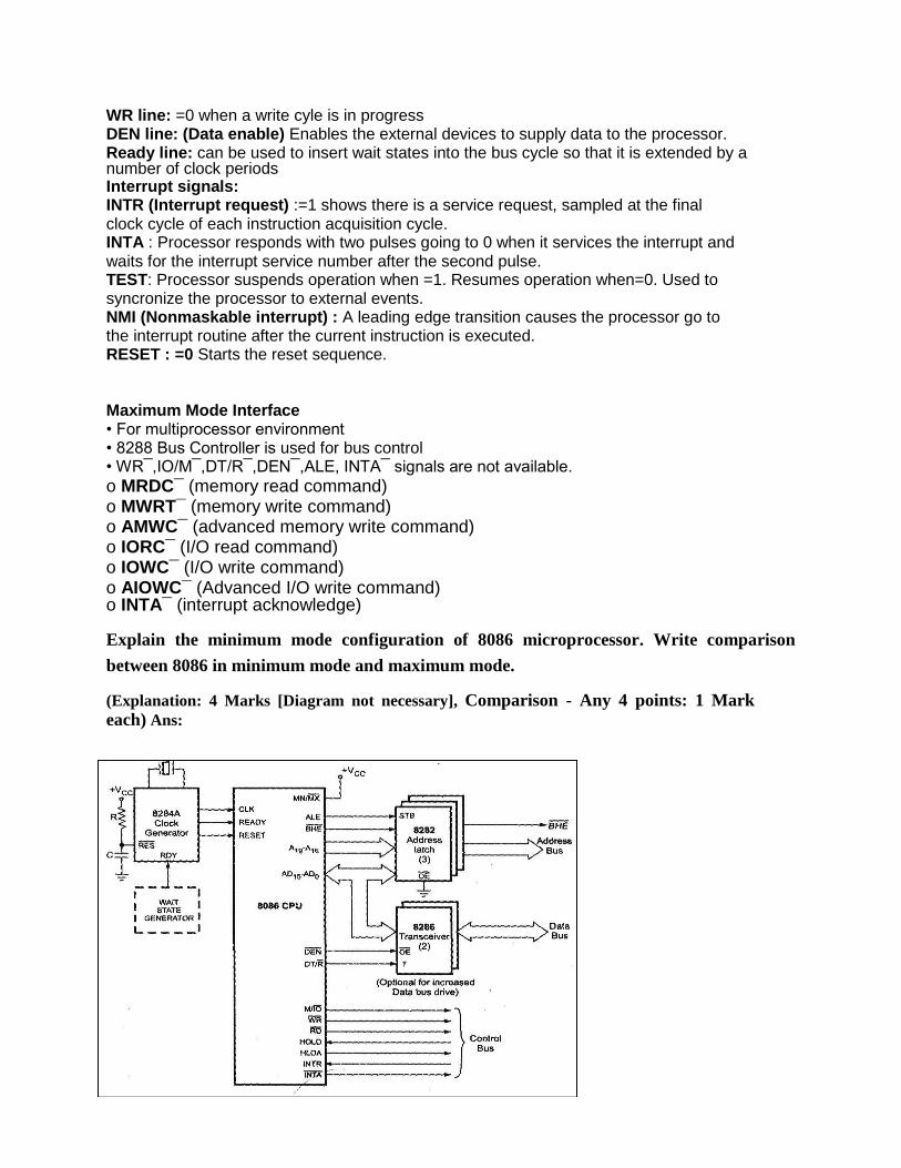
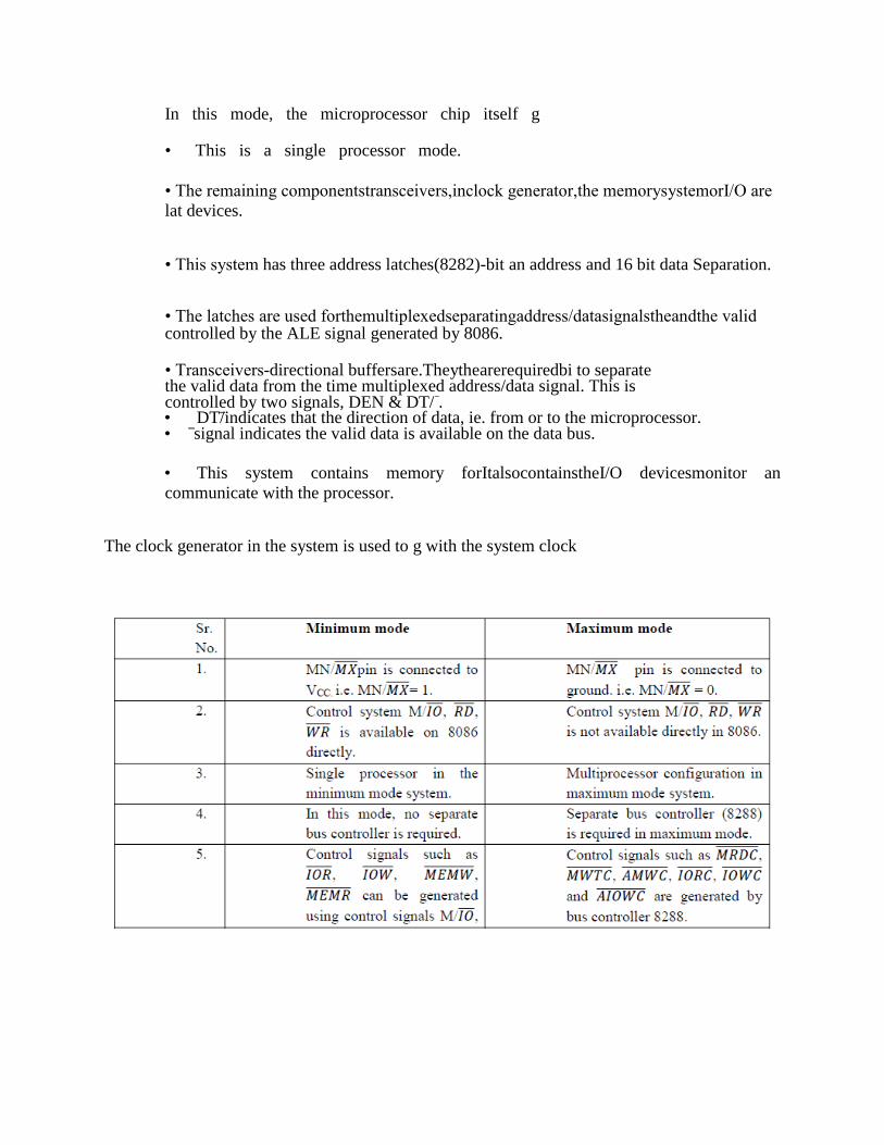
Explain the minimum mode configuration of 8086 microprocessor. Write comparison
between 8086 in minimum mode and maximum mode. (Explanation: 4 Marks [Diagram not necessary], Comparison - Any 4 points: 1 Mark each) Ans:
In this mode, the microprocessor chip itself g
• This is a single processor mode.
• The remaining componentstransceivers,inclock generator,the memorysystemorI/O are
lat devices.
• This system has three address latches(8282)-bit an address and 16 bit data Separation.
• The latches are used forthemultiplexedseparatingaddress/datasignalstheandthe valid controlled by the ALE signal generated by 8086.
• Transceivers-directional buffersare.Theythearerequiredbi to separate the valid data from the time multiplexed address/data signal. This is controlled by two signals, DEN & DT/ . • DT/ indicates that the direction of data, ie. from or to the microprocessor. • signal indicates the valid data is available on the data bus.
• This system contains memory forItalsocontainstheI/O devicesmonitor an
communicate with the processor. The clock generator in the system is used to g with the system clock
Addressing Modes A] Data Category B] Branch Category Data Category: 1)Immediate Addressing 2) Direct Addressing ( Segment Override prefix) 3) Register addressing 4) Register Indirect Addressing . 5)Register relative addressing.6)Base Index addressing 7)Relative base index addressing. Branch Category:
1) IntrasegmentDirect 2) IntersegmentIndirect.
3. Describe various addressing mode used in 8086 instructions with example.
(Any 4 addressing modes : ½ Mark explanation, ½ Mark one example of each) Ans: Different addressing modes of 8086 :
Immediate : In this addressing mode, immediate data is a part of instruction, and appears in the form of successive byte or word. E.g.: MOV AX, 005OH
Direct : In the direct addressing mode, a 16 bit address (offset) is directly specified in the instruction as a part of it. E.g.:. MOV AX ,[1 0 0 0 H]
Register : In register addressing mode, the data is stored in a register and it is referred using
the
particular register. All the registers except IP may be used in this mode. E.g.:. 1)MOV AX,BX 2)ROR AL,CL 3) AND AL,BL
4. Register Indirect: In this addressing mode, the address of the memory location which contains
data or operand is determined in an indirect way using offset registers. The offset address of data
is in either BX or SI or DI register. The default segment register is either DS or ES.
e.g. MOV AX, BX
5. Indexed : In this addressing mode offset of the operand is stored in one of the index register. DS and ES are the default segments for index registers SI and DI respectively
e.g. MOV AX, SI
6. Register Relative : In this addressing mode, the data is available at an effective address
formed by adding an 8-bit or 16-bit displacement with the content of any one of the registers BX,
BP, SI and DI in the default either DS or ES segment.
e.g. MOV AX, 50H BX
7. Based Indexed: In this addressing mode, the effective address of the data is formed by adding
the content of a base register (any one of BX or BP) to the content of an index register (any one of
SI or DI). The default segment register may be ES or DS.
e.g MOV AX, BX SI 8. Relative Based Indexed : The effective address is formed by adding an 8-bit or 16-bit
displacement with the sum of contents of any one of the base register (BX or BP) and any one of
the index registers in a default segment.
e.g. MOV AX, 50H BX SI
9. Implied addressing mode:
No address is required because the address or the operand is implied in the instruction itself. E.g NOP,STC,CLI,CLD,STD
Concept of pipelining
A technique used in advanced microprocessors where the microprocessor begins executing a
second instruction before the first has been completed. That is, several instructions are in the
pipeline simultaneously, each at a different processing stage.
The pipeline is divided into segments and each segment can execute its operation concurrently
with the other segments. When a segment completes an operation, it passes the result to the next
segment in the pipeline and fetches the next operation from the preceding segment. The final
results of each instruction emerge at the end of the pipeline in rapid succession.
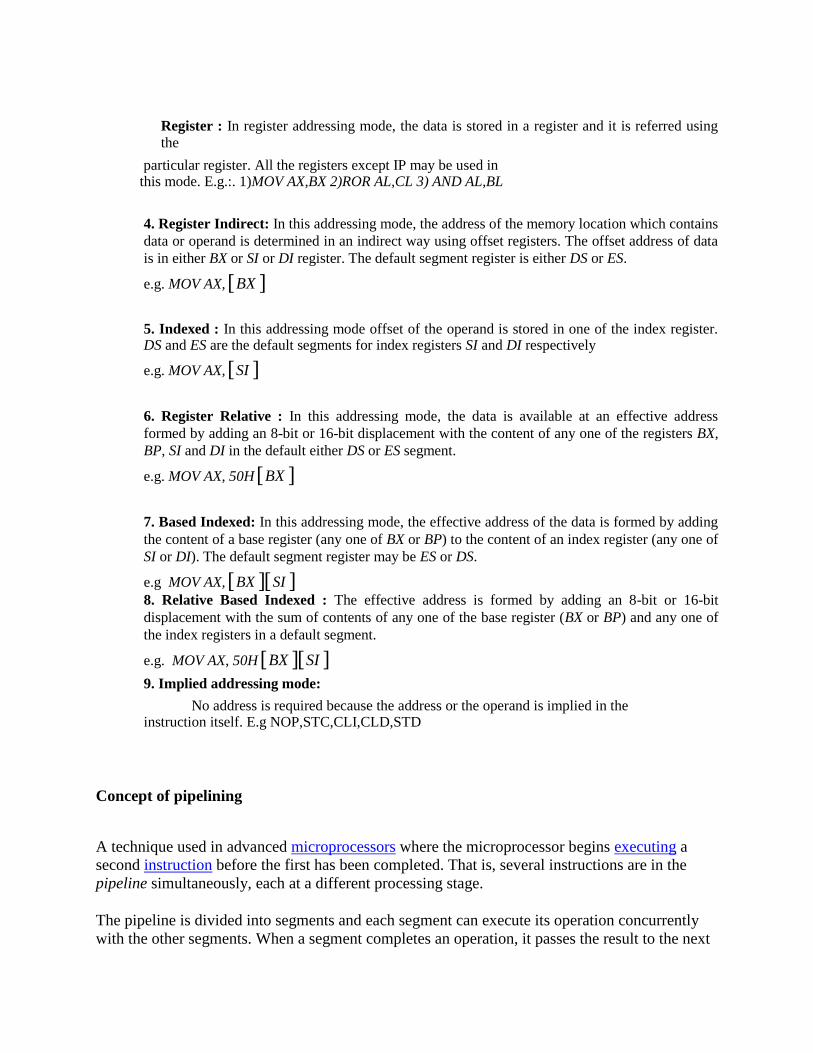
FETCH AND EXECUTE
Although the 8086/88 still functions as a stored program computer, organization of the CPU into
a separate BIU and EU allows the fetch and execute cycles to overlap. To see this, consider what
happens when the 8086 or 8088 is first started.
1. The BIU outputs the contents of the instruction pointer register (IP) onto the address bus,
causing the selected byte or word to be read into the BIU.
2. Register IP is incremented by 1 to prepare for the next instruction fetch.
3. Once inside the BIU, the instruction is passed to the queue. This is a first-in, first-out storage
register sometimes likened to a "pipeline".
4. Assuming that the queue is initially empty, the EU immediately draws this instruction from
the queue and begins execution.
5. While the EU is executing this instruction, the BIU proceeds to fetch a new instruction.
Depending on the execution time of the first instruction, the BIU may fill the queue with several
new instructions before the EU is ready to draw its next instruction.
The BIU is programmed to fetch a new instruction whenever the queue has room for one (with
the 8088) or two (with the 8086) additional bytes. The advantage of this pipelined architecture is
that the EU can execute instructions almost continually instead of having to wait for the BIU to
fetch a new instruction.
There are three conditions that will cause the EU to enter a "wait" mode. The first occurs when
an instruction requires access to a memory location not in the queue. The BIU must suspend
fetching instructions and output the address of this memory location. After waiting for the
memory access, the EU can resume executing instruction codes from the queue (and the BIU can
resume filling the queue).
The second condition occurs when the instruction to be executed is a "jump" instruction. In this
case control is to be transferred to a new (nonsequential) address. The queue, however, assumes
that instructions will always be executed in sequence and thus will be holding the "wrong"
instruction codes. The EU must wait while the instruction at the jump address is fetched. Note
that any bytes presently in the queue must be discarded (they are overwritten).
One other condition can cause the BIU to suspend fetching instructions. This occurs during
execution of instructions that are slow to execute. For example, the instruction AAM (ASCII
Adjust for Multiplication) requires 83 clock cycles to complete. At four cycles per instruction
fetch, the queue will be completely filled during the execution of this single instruction. The BIU
will thus have to wait for the EU to pull over one or two bytes from the queue before resuming
the fetch cycle.
A subtle advantage to the pipelined architecture should be mentioned. Because the next several
instructions are usually in the queue, the BIU can access memory at a somewhat "leisurely" pace.
This means that slow-mem parts can be used without affecting overall system performance.
f) Explain pipelining in 8086 microprocessor. How is queuing useful in
speeding up the Operation of 8086 microprocessor.
( Pipelining 3 Marks, usefulness
1 Mark) Ans:
In 8086, pipelining is the technique of overlapping instruction fetch and execution
mechanism.
To speed up program execution, the BIU fetches as many as six instruction bytes
ahead of time from memory. The size of instruction preftech queue in 8086 is 6 bytes.
While executing one instruction other instruction can be fetched. Thus it avoids the
waiting time for execution unit to receive other instruction.
BIU stores the fetched instructions in a 6 level deep FIFO . The BIU can be fetching
instructions bytes while the EU is decoding an instruction or executing an instruction
which does not require use of the buses.
When the EU is ready for its next instruction, it simply reads the instruction from the
queue in the BIU.
This is much faster than sending out an address to the system memory and waiting for

memory to send back the next instruction byte or bytes.
This improves overall speed of the processor.
MEMORY MAP
Still another view of the 8086/88 memory space could be as 16 64K-byte blocks beginning at
hex address 000000h and ending at address 0FFFFFh. This division into 64K-byte blocks is an
arbitrary but convenient choice. This is because the most significant hex digit increments by 1
with each additional block. That is, address 20000h is 65.536 bytes higher in memory than
address 10000h. Be sure to note that five hex digits are required to represent a memory address
The diagram is called a memory map. This is because, like a road map, it is a guide showing how
the system memory is allocated. This type of information is vital to the programmer, who must
know exactly where his or her programs can be safely loaded.
LOGICAL AND PHYSICAL ADDRESS
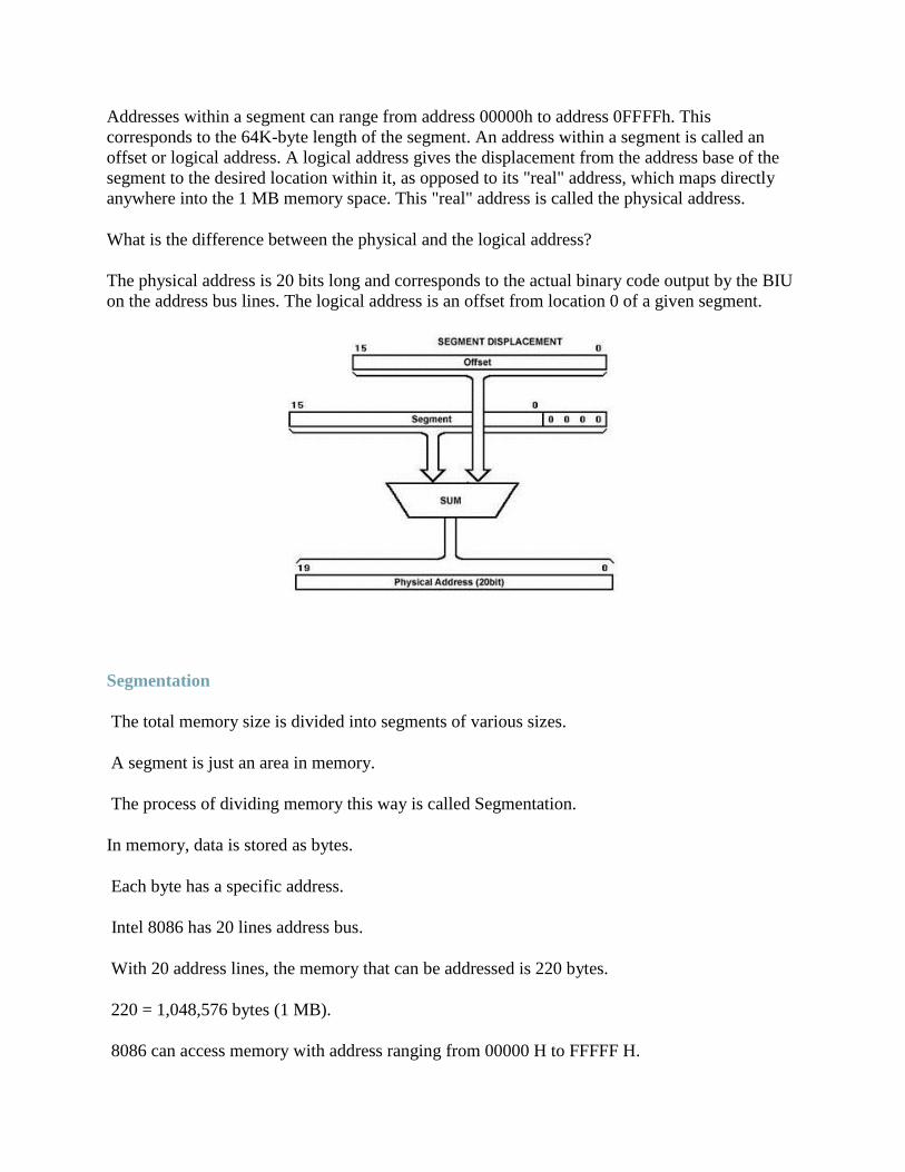
Addresses within a segment can range from address 00000h to address 0FFFFh. This
corresponds to the 64K-byte length of the segment. An address within a segment is called an
offset or logical address. A logical address gives the displacement from the address base of the
segment to the desired location within it, as opposed to its "real" address, which maps directly
anywhere into the 1 MB memory space. This "real" address is called the physical address.
What is the difference between the physical and the logical address?
The physical address is 20 bits long and corresponds to the actual binary code output by the BIU
on the address bus lines. The logical address is an offset from location 0 of a given segment.
Segmentation.
The total memory size is divided into segments of various sizes.
A segment is just an area in memory.
The process of dividing memory this way is called Segmentation.
In memory, data is stored as bytes.
Each byte has a specific address.
Intel 8086 has 20 lines address bus.
With 20 address lines, the memory that can be addressed is 220 bytes.
220 = 1,048,576 bytes (1 MB).
8086 can access memory with address ranging from 00000 H to FFFFF H.
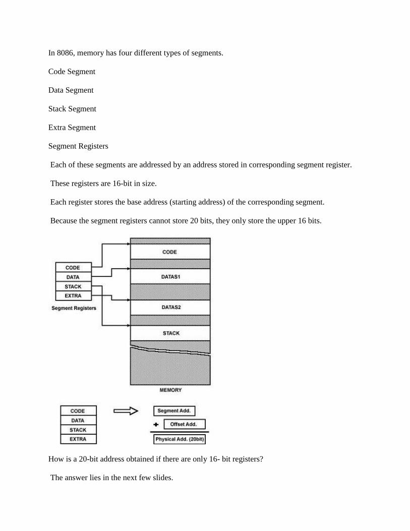
In 8086, memory has four different types of segments.
Code Segment
Data Segment
Stack Segment
Extra Segment
Segment Registers
Each of these segments are addressed by an address stored in corresponding segment register.
These registers are 16-bit in size.
Each register stores the base address (starting address) of the corresponding segment.
Because the segment registers cannot store 20 bits, they only store the upper 16 bits.
How is a 20-bit address obtained if there are only 16- bit registers?
The answer lies in the next few slides.

The 20-bit address of a byte is called its Physical Address.
But, it is specified as a Logical Address.
Logical address is in the form of: Base Address : Offset
Offset is the displacement of the memory location from the starting location of the segment.
Example
The value of Data Segment Register (DS) is 2222 H.
To convert this 16-bit address into 20-bit, the BIU appends 0H to the LSBs of the address.
After appending, the starting address of the Data Segment becomes 22220H.
If the data at any location has a logical address specified as: 2222 H : 0016 H
Then, the number 0016 H is the offset.
2222 H is the value of DS.
To calculate the effective address of the memory, BIU uses the following formula:
Effective Address = Starting Address of Segment + Offset
To find the starting address of the segment, BIU appends the contents of Segment Register with
0H.
Then, it adds offset to it.
Therefore:
EA = 22220 H
+ 0016 H
22236 H
Max. Size of Segment
All offsets are limited to 16-bits.
It means that the maximum size possible for segment is 2^16= 65,535 bytes (64 KB).
The offset of the first location within the segment is 0000 H.

The offset of the last location in the segment is FFFF H.
Where to look Segment address-
Describe how 20 bit physical address is generated in 8086 microprocessor. Give
one example.
(Description –2 Marks , Example –2 Marks)
Ans: Formation of a physical address:- Segment registers carry 16 bit data,
which is also known as base address. BIU attaches 0 as LSB of the base address.
So now this address becomes 20-bit address. Any base/pointer or index register
carry 16 bit offset. Offset address is added into 20-bit base address which finally
forms 20 bit physical address of memory location.
Example:- Assume DS= 2632H, SI=4567H
DS : 26320H.added by ……..BIU(orHardwired 0) + SI : 4567H
---------------------------- 2A887H
( OR Any Same Type of Example can be considered)
ADVANTAGES OF SEGMENTED MEMORY
Segmented memory can seem confusing at first. What you must remember is that the program
op-codes will be fetched from the code segment, while program data variables will be stored in
the data and extra segments. Stack operations use registers BP or SP and the stack segment. As
we begin writing programs the consequences of these definitions will become clearer.
An immediate advantage of having separate data and code segments is that one program can
work on several different sets of data. This is done by reloading register DS to point to the new
data. Perhaps the greatest advantage of segmented memory is that programs that reference
logical addresses only can be loaded and run anywhere in memory. This is because the logical
addresses always range from 00000h to 0FFFFh, independent of the code segment base. Such
programs are said to be relocatable, meaning that they will run at any location in memory. The
requirements for writing relocatable programs are that no references be made to physical
addresses, and no changes to the segment registers are allowed.
Describe memory segmentation in 8086 microprocessor and list it‟s four advantages.
Ans : (Description: 2 Marks, Any 4 Advantages : ½ Mark each)
Memory Segmentation: The memory in 8086 based system is organized as
segmented memory. 8086 can access 1Mbyte memory which is divided into
number of logical segments. Each segment is 64KB in size and addressed by
one of the segment register. The 4 segment register in BIU hold the 16-bit
starting address of 4 segments. CS holds program instruction code. Stack
segment stores interrupt & subroutine address. Data segment stores data for
program. Extra segment is used for string data.
Advantages of segmentation
1) With the use of segmentation the instruction and data is never overlapped.
2) The major advantage of segmentation is Dynamic relocatability of program which means
that a program can easily be transferred from one code memory segment to another code
memory segment without changing the effective address.
3) Segmentation can be used in multi-user time shared system. 4) Segmentation allows two processes to share data.
5) Segmentation allows you to extend the addressability of a processor i.e., address up to
1MB although the actual addresses to be handled are of 16 bit size. 6) Programs and data can be stored separately from each other in segmentation.
AN INTRODUCTION TO INTERRUPTS INTERRUPTS There are two main types of interrupt in the 8086 microprocessor, internal and external hardware interrupts. Hardware interrupts occur when a peripheral device asserts an interrupt input pin of the microprocessor. Whereas internal interrupts are initiated by the state of the CPU (e.g. divide
by zero error) or by an instruction. Provided the interrupt is permitted, it will be acknowledged by the processor at the end of the current memory cycle. The processor then services the interrupt by branching to a special service routine written to handle that particular interrupt. Upon servicing the device, the processor is then instructed to continue with what is was doing previously by use of the "return from interrupt" instruction. The status of the programme being executed must first be saved. The processors registers will be saved on the stack, or, at very least, the programme counter will be saved. Preserving those registers which are not saved will be the responsibility of the interrupt service routine. Once the programme counter has been saved, the processor will branch to the address of the service
routine.
Edge or Level sensitive Interrupts Edge level interrupts are recognised on the falling or rising edge of the input signal. They are generally used for high priority interrupts and are latched internally inside the processor. If this latching was not done, the processor could easily miss the falling edge (due to its short duration) and thus not respond to the interrupt request. Level sensitive interrupts overcome the problem of latching, in that the requesting device holds the interrupt line at a specified logic state (normally logic zero) till the processor acknowledges the interrupt. This type of interrupt can be shared by other devices in a wired 'OR' configuration, which is commonly used to support daisy chaining and other techniques. Maskable Interrupts The processor can inhibit certain types of interrupts by use of a special interrupt mask bit. This mask bit is part of the flags/condition code register, or a special interrupt register. In the 8086 microprocessor if this bit is clear, and an interrupt request occurs on the Interrupt Request input, it is ignored. Non-Maskable Interrupts There are some interrupts which cannot be masked out or ignored by the processor. These are associated with high priority tasks which cannot be ignored (like memory parity or bus faults). In general, most processors support the Non-Maskable Interrupt (NMI). This interrupt has absolute priority, and when it occurs, the processor will finish the current memory cycle, then branch to a special routine written to handle the interrupt request. Advantages of Interrupts Interrupts are used to ensure adequate service response times by the processing. Sometimes, with software polling routines, service times by the processor cannot be guaranteed, and data may be lost. The use of interrupts guarantees that the processor will service the request within a specified
time period, reducing the likelihood of lost data.
Interrupt Latency The time interval from when the interrupt is first asserted to the time the CPU recognises it. This

will depend much upon whether interrupts are disabled, prioritized and what the processor is currently executing. At times, a processor might ignore requests whilst executing some indivisible instruction stream (read-write-modify cycle). The figure that matters most is the longest possible interrupt latency time. Interrupt Response Time The time interval between the CPU recognising the interrupt to the time when the first instruction of the interrupt service routine is executed. This is determined by the processor architecture and clock speed. The Operation of an Interrupt sequence on the 8086 Microprocessor: 1. External interface sends an interrupt signal, to the Interrupt Request (INTR) pin, or an internal interrupt occurs. 2. The CPU finishes the present instruction (for a hardware interrupt) and sends Interrupt Acknowledge (INTA) to hardware interface. 3. The interrupt type N is sent to the Central Processor Unit (CPU) via the Data bus from the hardware interface. 4. The contents of the flag registers are pushed onto the stack. 5. Both the interrupt (IF) and (TF) flags are cleared. This disables the INTR pin and the trap or
single-step feature.
6. The contents of the code segment register (CS) are pushed onto the Stack. 7. The contents of the instruction pointer (IP) are pushed onto the Stack. 8. The interrupt vector contents are fetched, from (4 x N) and then placed into the IP and from (4 x N +2) into the CS so that the next instruction executes at the interrupt service procedure addressed by the interrupt vector. 9. While returning from the interrupt-service routine by the Interrupt Return (IRET) instruction, the IP, CS and Flag registers are popped from the Stack and return to their state prior to the
interrupt.
Multiple Interrupts If more than one device is connected to the interrupt line, the processor needs to know to which device service routine it should branch to. The identification of the device requesting service can be done in either hardware or software, or a combination of both. The three main methods are: 1. Software Polling, 2. Hardware Polling, (Daisy Chain),
3. Hardware Identification (Vectored Interrupts).
Explain maskable and non maskable interrupt used in 8086.
( Maskable any two points : 2Marks; non maskable any two points : 2Marks) Ans:
Non-Maskable interrupt:
8086 has a non-maskable interrupt input pin (NMI) that has highest priority among the external interrupts.
The NMI is not maskable internally by software. TRAP (single step-type1) is an internal interrupt having highest priority
amongst all the interrupts except Divide by Zero (Type 0) exception. The NMI is activated on a positive transition (low to high voltage). The NMI pin should remain high for at least two clock cycles and need not
synchronized with the clock for being sensed.
Maskable interrupt:
8086 also provides a INTR pin, that has lower priority as compared to NMI. The INTR signal is level triggered and can be masked by resetting the interrupt
flag. It is internally synchronized with the high transition of the CLK. For the INTR signal, to be responded to in the next instruction cycle; it must go
high in the last clock cycle of the current instruction or before that.
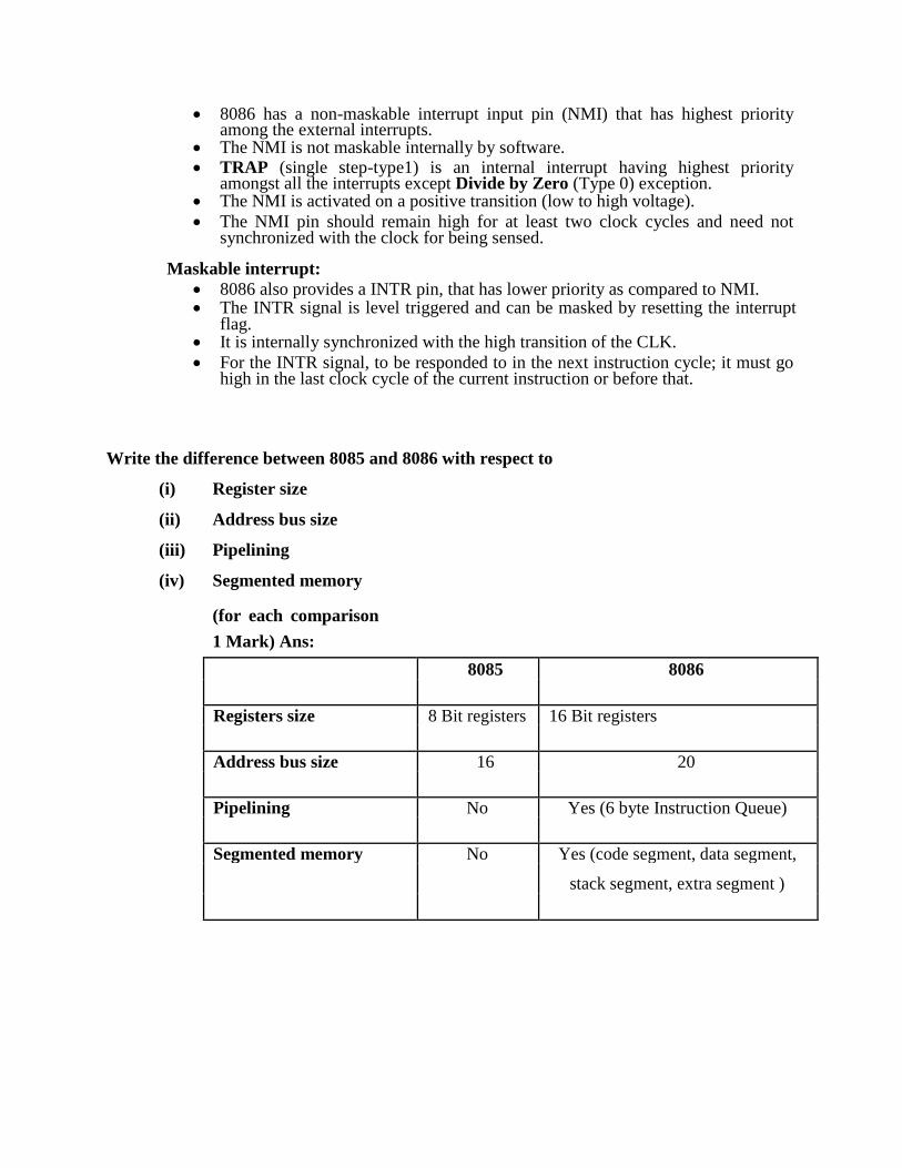
Write the difference between 8085 and 8086 with respect to
(i) Register size
(ii) Address bus size
(iii) Pipelining
(iv) Segmented memory
(for each comparison
1 Mark) Ans:
8085 8086
Registers size 8 Bit registers 16 Bit registers
Address bus size 16 20
Pipelining No Yes (6 byte Instruction Queue)
Segmented memory No Yes (code segment, data segment,
stack segment, extra segment )
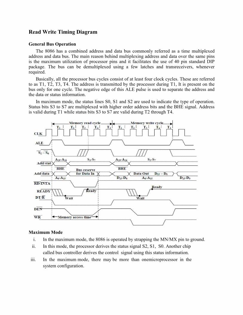
Read Write Timing Diagram
General Bus Operation
The 8086 has a combined address and data bus commonly referred as a time multiplexed address and data bus. The main reason behind multiplexing address and data over the same pins is the maximum utilization of processor pins and it facilitates the use of 40 pin standard DIP package. The bus can be demultiplexed using a few latches and transreceivers, whenever required.
Basically, all the processor bus cycles consist of at least four clock cycles. These are referred to as T1, T2, T3, T4. The address is transmitted by the processor during T1, It is present on the bus only for one cycle. The negative edge of this ALE pulse is used to separate the address and the data or status information.
In maximum mode, the status lines S0, S1 and S2 are used to indicate the type of operation. Status bits S3 to S7 are multiplexed with higher order address bits and the BHE signal. Address is valid during T1 while status bits S3 to S7 are valid during T2 through T4.
Maximum Mode
i. In the maximum mode, the 8086 is operated by strapping the MN/MX pin to ground.
ii. In this mode, the processor derives the status signal S2, S1, S0. Another chip called bus controller derives the control signal using this status information.
iii. In the maximum mode, there may be more than onemicroprocessor in the
system configuration.

Minimum Mode
i. In a minimum mode 8086 system, the microprocessor 8086is operated in
minimum mode by strapping its MN/MX pin to logic 1.
ii. In this mode, all the control signals are given out by the microprocessor chip itself.