Embed Size (px)
Citation preview
Serial Input, 14-Bit/16-Bit DAC
AD7849
Rev. C Information furnished by Analog Devices is believed to be accurate and reliable. However, no responsibility is assumed by Analog Devices for its use, nor for any infringements of patents or other rights of third parties that may result from its use. Specifications subject to change without notice. No license is granted by implication or otherwise under any patent or patent rights of Analog Devices. Trademarks and registered trademarks are the property of their respective owners.
One Technology Way, P.O. Box 9106, Norwood, MA 02062-9106, U.S.A.Tel: 781.329.4700 www.analog.com Fax: 781.461.3113 ©1995–2011 Analog Devices, Inc. All rights reserved.
FEATURES 14-bit/16-bit multiplying DAC Guaranteed monotonicity Output control on power-up and power-down internal or
external control Versatile serial interface DAC clears to 0 V in both unipolar and bipolar output ranges
APPLICATIONS Industrial process controls PC analog I/O boards Instrumentation
FUNCTIONAL BLOCK DIAGRAM VDD VCC
R
R
R
R
R
AD7849
ROFS
RST IN
VOUT
AGND
RST OUT
G1
G2
SDIN SCLK SYNC CLR BIN/COMP
DCEN SDOUT LDAC VSSDGND
DACLATCH
10/12
10/12
10-BIT/12-BITDAC
A1
A2
16-S
EGM
ENT
SWIT
CH
MA
TRIX
4
VREF+
VREF–
A3
LOGICCIRCUITRY
VOLTAGEMONITOR
INPUTLATCH
INPUT SHIFT REGISTER/CONTROL LOGIC
0100
8-00
1
Figure 1.
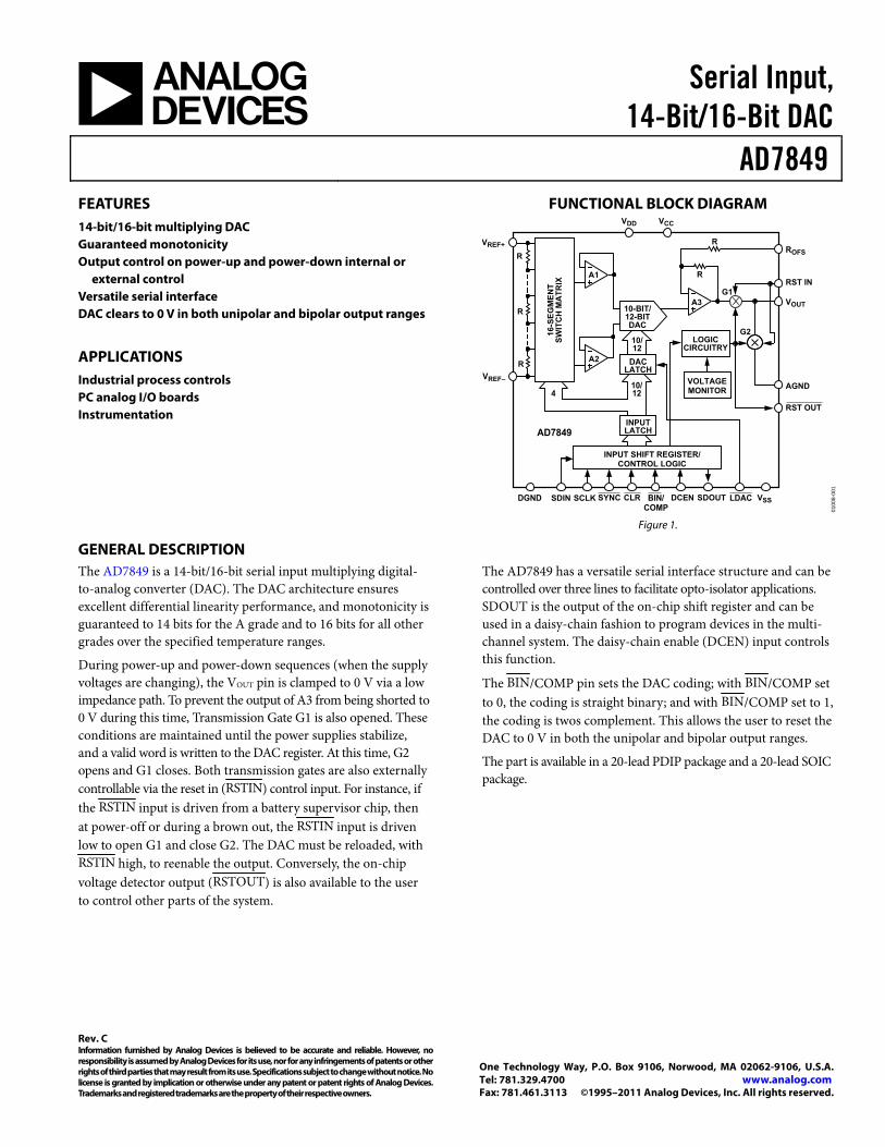
GENERAL DESCRIPTION The AD7849 is a 14-bit/16-bit serial input multiplying digital-to-analog converter (DAC). The DAC architecture ensures excellent differential linearity performance, and monotonicity is guaranteed to 14 bits for the A grade and to 16 bits for all other grades over the specified temperature ranges.
During power-up and power-down sequences (when the supply voltages are changing), the VOUT pin is clamped to 0 V via a low impedance path. To prevent the output of A3 from being shorted to 0 V during this time, Transmission Gate G1 is also opened. These conditions are maintained until the power supplies stabilize, and a valid word is written to the DAC register. At this time, G2 opens and G1 closes. Both transmission gates are also externally controllable via the reset in (RSTIN) control input. For instance, if the RSTIN input is driven from a battery supervisor chip, then at power-off or during a brown out, the RSTIN input is driven low to open G1 and close G2. The DAC must be reloaded, with RSTIN high, to reenable the output. Conversely, the on-chip voltage detector output (RSTOUT) is also available to the user to control other parts of the system.
The AD7849 has a versatile serial interface structure and can be controlled over three lines to facilitate opto-isolator applications. SDOUT is the output of the on-chip shift register and can be used in a daisy-chain fashion to program devices in the multi-channel system. The daisy-chain enable (DCEN) input controls this function.
The BIN/COMP pin sets the DAC coding; with BIN/COMP set to 0, the coding is straight binary; and with BIN/COMP set to 1, the coding is twos complement. This allows the user to reset the DAC to 0 V in both the unipolar and bipolar output ranges.
The part is available in a 20-lead PDIP package and a 20-lead SOIC package.
AD7849* Product Page Quick LinksLast Content Update: 10/05/2016
Comparable PartsView a parametric search of comparable parts
DocumentationData Sheet• AD7849: Serial Input, 14-Bit/16-Bit DAC Data Sheet
Reference MaterialsSolutions Bulletins & Brochures• Digital to Analog Converters ICs Solutions Bulletin
Design Resources• AD7849 Material Declaration• PCN-PDN Information• Quality And Reliability• Symbols and Footprints
DiscussionsView all AD7849 EngineerZone Discussions
Sample and BuyVisit the product page to see pricing options
Technical SupportSubmit a technical question or find your regional support number
* This page was dynamically generated by Analog Devices, Inc. and inserted into this data sheet. Note: Dynamic changes to the content on this page does not constitute a change to the revision number of the product data sheet. This content may be frequently modified.
AD7849
Rev. C | Page 2 of 20
TABLE OF CONTENTS Features .............................................................................................. 1
Applications....................................................................................... 1
Functional Block Diagram .............................................................. 1
General Description ......................................................................... 1
Revision History ............................................................................... 2
Specifications..................................................................................... 3
Reset Specifications ...................................................................... 4
AC Performance Characteristics ................................................ 5
Timing Characteristics ................................................................ 5
Absolute Maximum Ratings............................................................ 6
ESD Caution.................................................................................. 6
Pin Configuration and Function Descriptions............................. 7
Typical Performance Characteristics ..............................................8
Terminology .................................................................................... 10
Circuit Description......................................................................... 11
Digital-to-Analog Conversion.................................................. 11
Digital Interface.......................................................................... 12
Applying the AD7849 ................................................................ 13
Microprocessor Interfacing....................................................... 15
Applications Information .............................................................. 17
Opto-Isolated Interface ............................................................. 17
Outline Dimensions ....................................................................... 18
Ordering Guide .......................................................................... 19
REVISION HISTORY 3/11—Rev. B to Rev. C Deleted 20-Lead CERDIP (Q-20) Package and T Version .............................................................................Universal Updated Format..................................................................Universal Deleted AD7849-to-ADSP-2101/ADSP-2102 Interface Section and Figure 20; Renumbered Sequentially.................................... 12
AD7849
Rev. C | Page 3 of 20
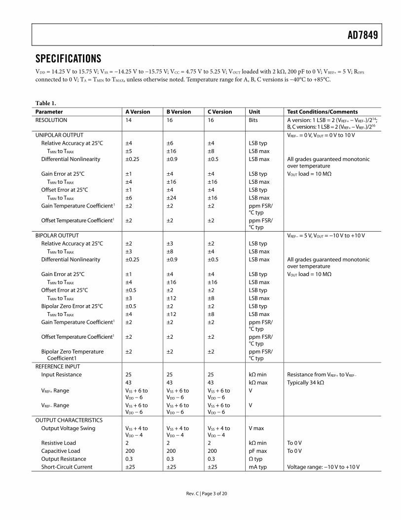
SPECIFICATIONS VDD = 14.25 V to 15.75 V; VSS = −14.25 V to −15.75 V; VCC = 4.75 V to 5.25 V; VOUT loaded with 2 kΩ, 200 pF to 0 V; VREF+ = 5 V; ROFS connected to 0 V; TA = TMIN to TMAX, unless otherwise noted. Temperature range for A, B, C versions is −40°C to +85°C.
Table 1. Parameter A Version B Version C Version Unit Test Conditions/Comments RESOLUTION 14 16 16 Bits A version: 1 LSB = 2 (VREF+ − VREF−)/214;
B, C versions: 1 LSB = 2 (VREF+ − VREF−)/216 UNIPOLAR OUTPUT VREF− = 0 V, VOUT = 0 V to 10 V
Relative Accuracy at 25°C ±4 ±6 ±4 LSB typ TMIN to TMAX ±5 ±16 ±8 LSB max
Differential Nonlinearity ±0.25 ±0.9 ±0.5 LSB max All grades guaranteed monotonic over temperature
Gain Error at 25°C ±1 ±4 ±4 LSB typ VOUT load = 10 MΩ TMIN to TMAX ±4 ±16 ±16 LSB max
Offset Error at 25°C ±1 ±4 ±4 LSB typ TMIN to TMAX ±6 ±24 ±16 LSB max
Gain Temperature Coefficient1 ±2 ±2 ±2 ppm FSR/ °C typ
Offset Temperature Coefficient1 ±2 ±2 ±2 ppm FSR/ °C typ
BIPOLAR OUTPUT VREF− = 5 V, VOUT = −10 V to +10 V Relative Accuracy at 25°C ±2 ±3 ±2 LSB typ
TMIN to TMAX ±3 ±8 ±4 LSB max Differential Nonlinearity ±0.25 ±0.9 ±0.5 LSB max All grades guaranteed monotonic
over temperature Gain Error at 25°C ±1 ±4 ±4 LSB typ VOUT load = 10 MΩ
TMIN to TMAX ±4 ±16 ±16 LSB max Offset Error at 25°C ±0.5 ±2 ±2 LSB typ
TMIN to TMAX ±3 ±12 ±8 LSB max Bipolar Zero Error at 25°C ±0.5 ±2 ±2 LSB typ
TMIN to TMAX ±4 ±12 ±8 LSB max Gain Temperature Coefficient1 ±2 ±2 ±2 ppm FSR/
°C typ
Offset Temperature Coefficient1 ±2 ±2 ±2 ppm FSR/ °C typ
Bipolar Zero Temperature Coefficient1
±2 ±2 ±2 ppm FSR/ °C typ
REFERENCE INPUT Input Resistance 25 25 25 kΩ min Resistance from VREF+ to VREF− 43 43 43 kΩ max Typically 34 kΩ VREF+ Range VSS + 6 to
VDD − 6 VSS + 6 to VDD − 6
VSS + 6 to VDD − 6
V
VREF− Range VSS + 6 to VDD − 6
VSS + 6 to VDD − 6
VSS + 6 to VDD − 6
V
OUTPUT CHARACTERISTICS Output Voltage Swing VSS + 4 to
VDD − 4 VSS + 4 to VDD − 4
VSS + 4 to VDD − 4
V max
Resistive Load 2 2 2 kΩ min To 0 V Capacitive Load 200 200 200 pF max To 0 V Output Resistance 0.3 0.3 0.3 Ω typ Short-Circuit Current ±25 ±25 ±25 mA typ Voltage range: −10 V to +10 V
AD7849
Rev. C | Page 4 of 20
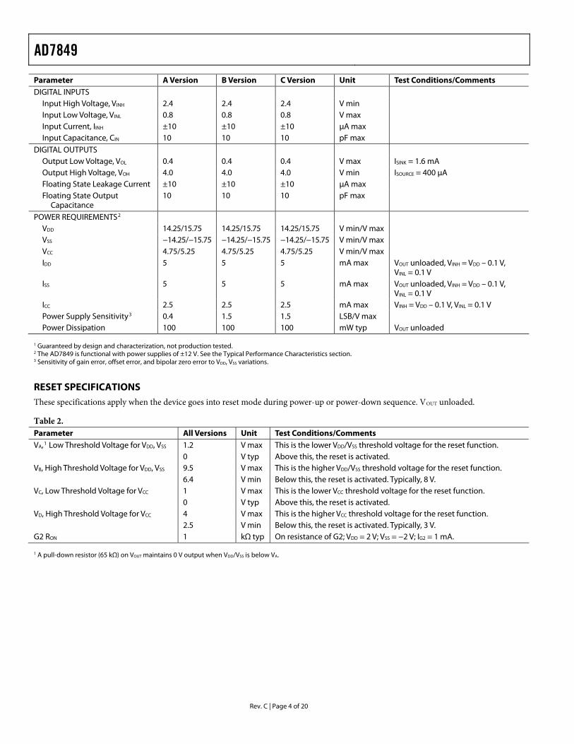
Parameter A Version B Version C Version Unit Test Conditions/Comments DIGITAL INPUTS
Input High Voltage, VINH 2.4 2.4 2.4 V min Input Low Voltage, VINL 0.8 0.8 0.8 V max Input Current, IINH ±10 ±10 ±10 μA max Input Capacitance, CIN 10 10 10 pF max
DIGITAL OUTPUTS Output Low Voltage, VOL 0.4 0.4 0.4 V max ISINK = 1.6 mA Output High Voltage, VOH 4.0 4.0 4.0 V min ISOURCE = 400 μA Floating State Leakage Current ±10 ±10 ±10 μA max Floating State Output
Capacitance 10 10 10 pF max
POWER REQUIREMENTS2 VDD 14.25/15.75 14.25/15.75 14.25/15.75 V min/V max VSS −14.25/−15.75 −14.25/−15.75 −14.25/−15.75 V min/V max VCC 4.75/5.25 4.75/5.25 4.75/5.25 V min/V max IDD 5 5 5 mA max VOUT unloaded, VINH = VDD – 0.1 V,
VINL = 0.1 V ISS 5 5 5 mA max VOUT unloaded, VINH = VDD – 0.1 V,
VINL = 0.1 V ICC 2.5 2.5 2.5 mA max VINH = VDD – 0.1 V, VINL = 0.1 V Power Supply Sensitivity3 0.4 1.5 1.5 LSB/V max Power Dissipation 100 100 100 mW typ VOUT unloaded
1 Guaranteed by design and characterization, not production tested. 2 The AD7849 is functional with power supplies of ±12 V. See the Typical Performance Characteristics section. 3 Sensitivity of gain error, offset error, and bipolar zero error to VDD, VSS variations.
RESET SPECIFICATIONS These specifications apply when the device goes into reset mode during power-up or power-down sequence. VOUT unloaded.
Table 2. Parameter All Versions Unit Test Conditions/Comments VA,1 Low Threshold Voltage for VDD, VSS 1.2 V max This is the lower VDD/VSS threshold voltage for the reset function. 0 V typ Above this, the reset is activated. VB, High Threshold Voltage for VDD, VSS 9.5 V max This is the higher VDD/VSS threshold voltage for the reset function. 6.4 V min Below this, the reset is activated. Typically, 8 V. VC, Low Threshold Voltage for VCC 1 V max This is the lower VCC threshold voltage for the reset function. 0 V typ Above this, the reset is activated. VD, High Threshold Voltage for VCC 4 V max This is the higher VCC threshold voltage for the reset function. 2.5 V min Below this, the reset is activated. Typically, 3 V. G2 RON 1 kΩ typ On resistance of G2; VDD = 2 V; VSS = −2 V; IG2 = 1 mA. 1 A pull-down resistor (65 kΩ) on VOUT maintains 0 V output when VDD/VSS is below VA.
AD7849
Rev. C | Page 5 of 20
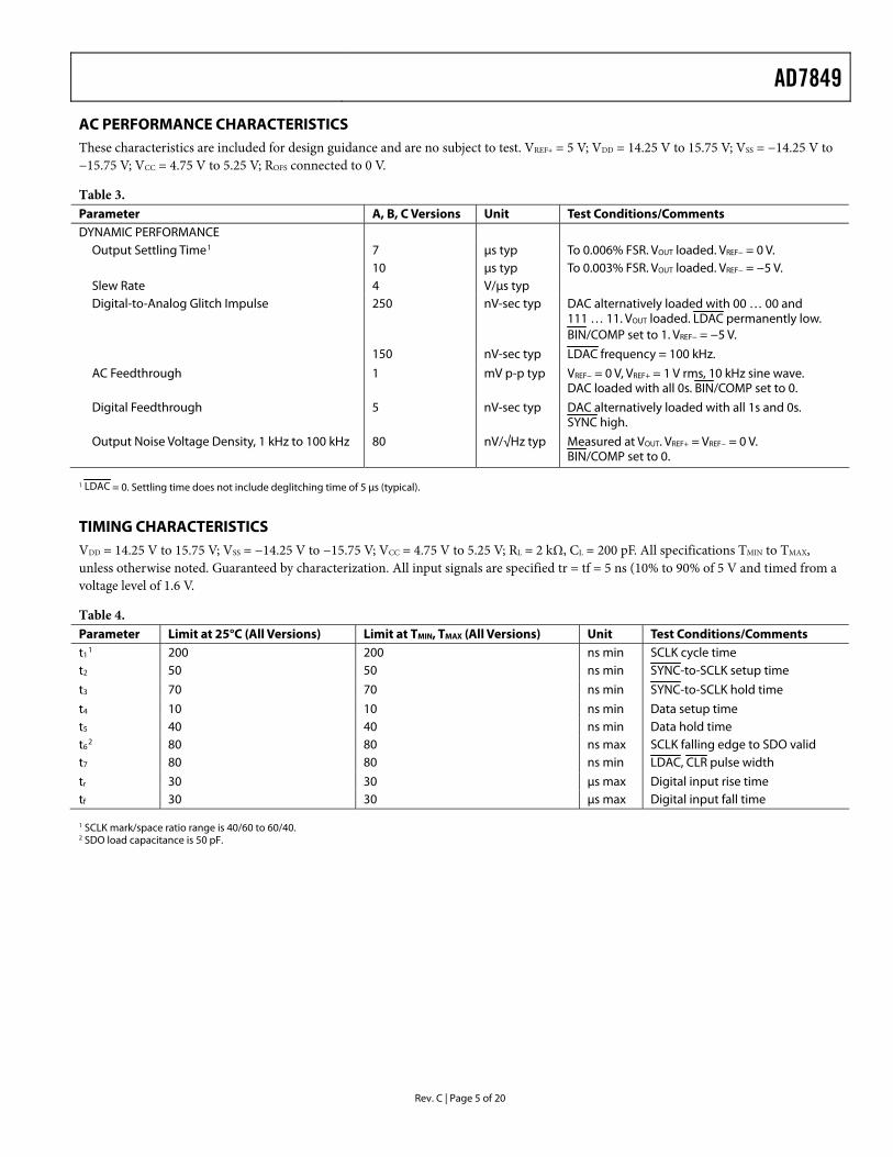
AC PERFORMANCE CHARACTERISTICS These characteristics are included for design guidance and are no subject to test. VREF+ = 5 V; VDD = 14.25 V to 15.75 V; VSS = −14.25 V to −15.75 V; VCC = 4.75 V to 5.25 V; ROFS connected to 0 V.
Table 3. Parameter A, B, C Versions Unit Test Conditions/Comments DYNAMIC PERFORMANCE
Output Settling Time1 7 μs typ To 0.006% FSR. VOUT loaded. VREF− = 0 V. 10 μs typ To 0.003% FSR. VOUT loaded. VREF− = −5 V. Slew Rate 4 V/μs typ Digital-to-Analog Glitch Impulse 250 nV-sec typ DAC alternatively loaded with 00 … 00 and
111 … 11. VOUT loaded. LDAC permanently low. BIN/COMP set to 1. VREF− = −5 V.
150 nV-sec typ LDAC frequency = 100 kHz.
AC Feedthrough 1 mV p-p typ VREF− = 0 V, VREF+ = 1 V rms, 10 kHz sine wave. DAC loaded with all 0s. BIN/COMP set to 0.
Digital Feedthrough 5 nV-sec typ DAC alternatively loaded with all 1s and 0s. SYNC high.
Output Noise Voltage Density, 1 kHz to 100 kHz 80 nV/√Hz typ Measured at VOUT. VREF+ = VREF− = 0 V. BIN/COMP set to 0.
1 LDAC = 0. Settling time does not include deglitching time of 5 μs (typical).
TIMING CHARACTERISTICS VDD = 14.25 V to 15.75 V; VSS = −14.25 V to −15.75 V; VCC = 4.75 V to 5.25 V; RL = 2 kΩ, CL = 200 pF. All specifications TMIN to TMAX, unless otherwise noted. Guaranteed by characterization. All input signals are specified tr = tf = 5 ns (10% to 90% of 5 V and timed from a voltage level of 1.6 V.
Table 4. Parameter Limit at 25°C (All Versions) Limit at TMIN, TMAX (All Versions) Unit Test Conditions/Comments t1
1 200 200 ns min SCLK cycle time t2 50 50 ns min SYNC-to-SCLK setup time
t3 70 70 ns min SYNC-to-SCLK hold time
t4 10 10 ns min Data setup time t5 40 40 ns min Data hold time t6
2 80 80 ns max SCLK falling edge to SDO valid t7 80 80 ns min LDAC, CLR pulse width
tr 30 30 μs max Digital input rise time tf 30 30 μs max Digital input fall time 1 SCLK mark/space ratio range is 40/60 to 60/40. 2 SDO load capacitance is 50 pF.
AD7849
Rev. C | Page 6 of 20
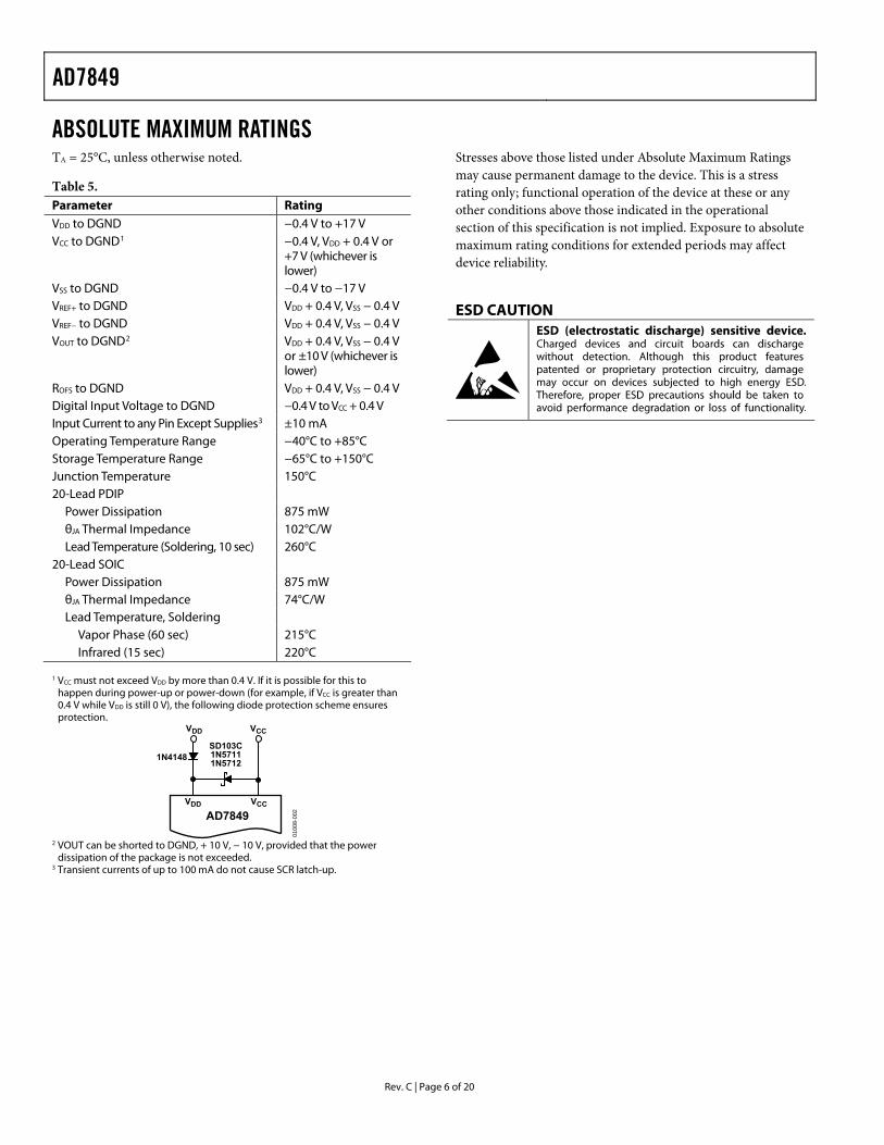
ABSOLUTE MAXIMUM RATINGS TA = 25°C, unless otherwise noted.
Table 5. Parameter Rating VDD to DGND −0.4 V to +17 V VCC to DGND1 −0.4 V, VDD + 0.4 V or
+7 V (whichever is lower)
VSS to DGND −0.4 V to −17 V VREF+ to DGND VDD + 0.4 V, VSS − 0.4 V VREF− to DGND VDD + 0.4 V, VSS − 0.4 V VOUT to DGND2 VDD + 0.4 V, VSS − 0.4 V
or ±10 V (whichever is lower)
ROFS to DGND VDD + 0.4 V, VSS − 0.4 V Digital Input Voltage to DGND −0.4 V to VCC + 0.4 V Input Current to any Pin Except Supplies3 ±10 mA Operating Temperature Range −40°C to +85°C Storage Temperature Range −65°C to +150°C Junction Temperature 150°C 20-Lead PDIP
Power Dissipation 875 mW θJA Thermal Impedance 102°C/W Lead Temperature (Soldering, 10 sec) 260°C
20-Lead SOIC Power Dissipation 875 mW θJA Thermal Impedance 74°C/W Lead Temperature, Soldering
Vapor Phase (60 sec) 215°C Infrared (15 sec) 220°C
1 VCC must not exceed VDD by more than 0.4 V. If it is possible for this to
happen during power-up or power-down (for example, if VCC is greater than 0.4 V while VDD is still 0 V), the following diode protection scheme ensures protection.
SD103C1N57111N5712
1N4148
VDD VCC
VDD VCC
AD7849
0100
8-00
2
2 VOUT can be shorted to DGND, + 10 V, − 10 V, provided that the power
dissipation of the package is not exceeded. 3 Transient currents of up to 100 mA do not cause SCR latch-up.
Stresses above those listed under Absolute Maximum Ratings may cause permanent damage to the device. This is a stress rating only; functional operation of the device at these or any other conditions above those indicated in the operational section of this specification is not implied. Exposure to absolute maximum rating conditions for extended periods may affect device reliability.
ESD CAUTION
AD7849
Rev. C | Page 7 of 20
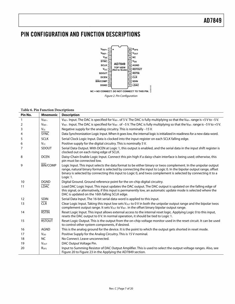
PIN CONFIGURATION AND FUNCTION DESCRIPTIONS
VREF+
VDD
NC
VOUT
ROFS
VREF–
VSS
SYNC
RSTINRSTOUTAGNDSCLK
VCC
SDOUTDCEN
BIN/COMPDGND LDAC
SDINCLR
1
2
3
4
20
19
18
17
5 16
6 15
7 14
8 13
9 12
10 11
NC = NO CONNECT. DO NOT CONNECT TO THIS PIN.
AD7849TOP VIEW
(Not to Scale)
0100
8-00
3
Figure 2. Pin Configuration
Table 6. Pin Function Descriptions Pin No. Mnemonic Description 1 VREF+ VREF+ Input. The DAC is specified for VREF+ of 5 V. The DAC is fully multiplying so that the VREF+ range is +5 V to –5 V. 2 VREF− VREF− Input. The DAC is specified for VREF− of –5 V. The DAC is fully multiplying so that the VREF− range is –5 V to +5 V. 3 VSS Negative supply for the analog circuitry. This is nominally –15 V. 4 SYNC Data Synchronization Logic Input. When it goes low, the internal logic is initialized in readiness for a new data-word.
5 SCLK Serial Clock Logic Input. Data is clocked into the input register on each SCLK falling edge. 6 VCC Positive supply for the digital circuitry. This is nominally 5 V. 7 SDOUT Serial Data Output. With DCEN at Logic 1, this output is enabled, and the serial data in the input shift register is
clocked out on each rising edge of SCLK. 8 DCEN Daisy-Chain Enable Logic Input. Connect this pin high if a daisy-chain interface is being used; otherwise, this
pin must be connected low. 9 BIN/COMP Logic Input. This input selects the data format to be either binary or twos complement. In the unipolar output
range, natural binary format is selected by connecting the input to Logic 0. In the bipolar output range, offset binary is selected by connecting this input to Logic 0, and twos complement is selected by connecting it to a Logic 1.
10 DGND Digital Ground. Ground reference point for the on-chip digital circuitry. 11 LDAC Load DAC Logic Input. This input updates the DAC output. The DAC output is updated on the falling edge of
this signal, or alternatively, if this input is permanently low, an automatic update mode is selected where the DAC is updated on the 16th falling SCLK edge.
12 SDIN Serial Data Input. The 16-bit serial data-word is applied to this input. 13 CLR Clear Logic Input. Taking this input low sets VOUT to 0 V in both the unipolar output range and the bipolar twos
complement output range. It sets VOUT to VREF– in the offset binary bipolar output range. 14 RSTIN Reset Logic Input. This input allows external access to the internal reset logic. Applying Logic 0 to this input,
resets the DAC output to 0 V. In normal operation, it should be tied to Logic 1. 15 RSTOUT Reset Logic Output. This is the output from the on-chip voltage monitor used in the reset circuit. It can be used
to control other system components, if desired. 16 AGND This is the analog ground for the device. It is the point to which the output gets shorted in reset mode. 17 VDD Positive Supply for the Analog Circuitry. This is 15 V nominal. 18 NC No Connect. Leave unconnected. 19 VOUT DAC Output Voltage Pin. 20 ROFS Input to Summing Resistor of DAC Output Amplifier. This is used to select the output voltage ranges. Also, see
Figure 20 to Figure 23 in the Applying the AD7849 section.
AD7849
Rev. C | Page 8 of 20
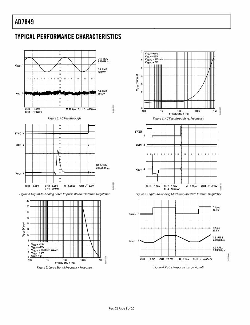
TYPICAL PERFORMANCE CHARACTERISTICS
FREQUENCY (Hz)
7
0100 1M1k
V OU
T(m
Vp-
p)
10k 100k
6
5
4
3
2
1
VDD = +15VVSS = –15VVREF+ = 1V rmsVREF– = 0V
0100
8-00
7
VREF+ 1
VOUT 4
C1 FREQ9.9942kHz
C1 RMS728mV
C4 RMS556µV
CH1 1.00VCH4 1.00mV
M 20.0µs CH1 –300mV01
008-
004
Figure 3. AC Feedthrough Figure 6. AC Feedthrough vs. Frequency
SYNC
SDIN
VOUT
1
2
4
C4 AREA247.964nVS
CH2 5.00VCH4 200mV
M 1.00µs CH1 3.7VCH1 5.00V
0100
8-00
5
1
4
2
LDAC
SDIN
VOUT
CH4 50.0mVCH2 5.00V M 5.00µs CH1 –2.3VCH1 5.00V
0100
8-00
8
Figure 4. Digital-to-Analog Glitch Impulse Without Internal Deglitcher Figure 7. Digital-to-Analog Glitch Impulse With Internal Deglitcher
FREQUENCY (Hz)100 1M1k 10k 100k
22
2
V OU
T(V
p-p)
20
18
16
14
12
10
8
6
4
VDD = +15VVSS = –15VVREF+ = ±5 SINE WAVEVREF– = 0VGAIN = 2
0100
8-00
6
1
2VOUT
VREF+
C1 p-p10.4V
C2 p-p20.8V
C2 RISE2.79230µs
C2 FALL3.20385µs
CH2 20.0V M 2.5µs CH1 –400mVCH1 10.0V 0100
8-00
9
Figure 8. Pulse Response (Large Signal) Figure 5. Large Signal Frequency Response
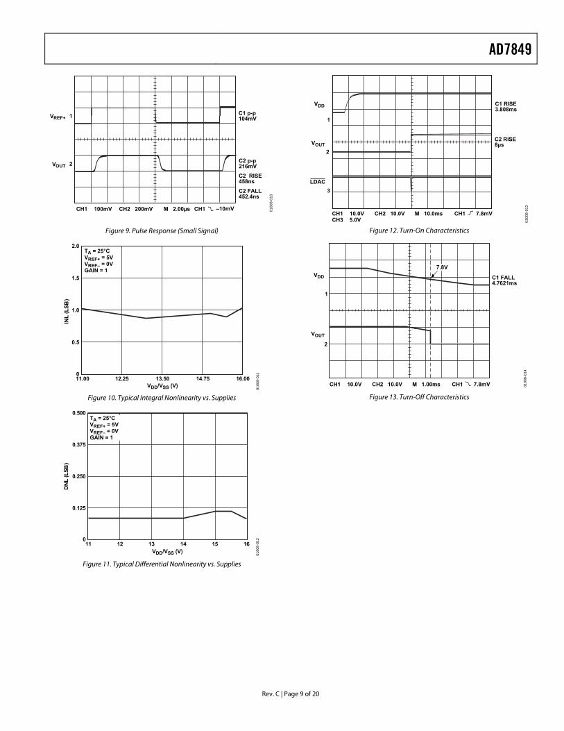
AD7849
Rev. C | Page 9 of 20
1
2VOUT
CH2 200mV M 2.00µs CH1 –10mVCH1 100mV
VREF+C1 p-p104mV
C2 p-p216mVC2 RISE458nsC2 FALL452.4ns
0100
8-01
0
Figure 9. Pulse Response (Small Signal)
VDD/VSS (V)
2.0
016.0011.00 12.25
INL
(LSB
)
13.50 14.75
1.5
1.0
0.5
TA = 25°CVREF+ = 5VVREF– = 0VGAIN = 1
0100
8-01
1
Figure 10. Typical Integral Nonlinearity vs. Supplies
0.500
01611 12
DNL
(LSB
)
13 14
0.375
0.250
0.125
15VDD/VSS (V)
TA = 25°CVREF+ = 5VVREF– = 0VGAIN = 1
0100
8-01
2
Figure 11. Typical Differential Nonlinearity vs. Supplies
CH2 10.0V M 10.0ms CH1 7.8mVCH1 10.0V
C1 RISE3.808ms
C2 RISE8µs
1
2
3
CH3 5.0V
VDD
VOUT
LDAC
0100
8-01
3
Figure 12. Turn-On Characteristics
CH2 10.0V M 1.00ms CH1 7.8mVCH1 10.0V
7.8V
1
2
VDD
VOUT
C1 FALL4.7621ms
0100
8-01
4
Figure 13. Turn-Off Characteristics
AD7849
Rev. C | Page 10 of 20
TERMINOLOGY Least Significant Bit This is the analog weighting of 1 bit of the digital word in a DAC. For the B version and the C versions, 1 LSB = (VREF+ − VREF−)/216. For the A version, 1 LSB = (VREF+ − VREF−)/214.
Relative Accuracy Relative accuracy or endpoint nonlinearity is a measure of the maximum deviation from a straight line passing through the endpoints of the DAC transfer function. It is measured after adjusting for both endpoints (that is, offset and gain errors are adjusted out) and is normally expressed in least significant bits or as a percentage of full-scale range.
Differential Nonlinearity Differential nonlinearity is the difference between the measured change and the ideal change between any two adjacent codes. A specified differential nonlinearity of less than ±1 LSB over the operating temperature range ensures monotonicity.
Gain Error Gain error is a measure of the output error between an ideal DAC and the actual device output with all 1s loaded after offset error has been adjusted out. Gain error is adjustable to zero with an external potentiometer.
Offset Error This is the error present at the device output with all 0s loaded in the DAC. It is due to the op amp input offset voltage and bias current and the DAC leakage current.
Bipolar Zero Error When the AD7849 is connected for bipolar output and (100 … 000) is loaded to the DAC, the deviation of the analog output from the ideal midscale of 0 V is called the bipolar zero error.
Digital-to-Analog Glitch Impulse This is the amount of charge injected from the digital inputs to the analog output when the inputs change state. Normally, this is specified as the area of the glitch in nV-secs.
Multiplying Feedthrough Error This is an ac error due to capacitive feedthrough from either of the VREF terminals to VOUT when the DAC is loaded with all 0s.
Digital Feedthrough When the DAC is not selected (SYNC is held high), high frequency logic activity on the digital inputs is capacitively coupled through the device to show up as noise on the VOUT pin. This noise is digital feedthrough.
AD7849
Rev. C | Page 11 of 20
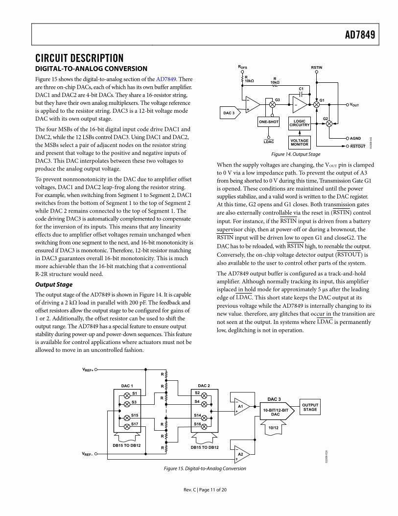
CIRCUIT DESCRIPTION DIGITAL-TO-ANALOG CONVERSION Figure 15 shows the digital-to-analog section of the AD7849. There are three on-chip DACs, each of which has its own buffer amplifier. DAC1 and DAC2 are 4-bit DACs. They share a 16-resistor string, but they have their own analog multiplexers. The voltage reference is applied to the resistor string. DAC3 is a 12-bit voltage mode DAC with its own output stage.
The four MSBs of the 16-bit digital input code drive DAC1 and DAC2, while the 12 LSBs control DAC3. Using DAC1 and DAC2, the MSBs select a pair of adjacent nodes on the resistor string and present that voltage to the positive and negative inputs of DAC3. This DAC interpolates between these two voltages to produce the analog output voltage.
To prevent nonmonotonicity in the DAC due to amplifier offset voltages, DAC1 and DAC2 leap-frog along the resistor string. For example, when switching from Segment 1 to Segment 2, DAC1 switches from the bottom of Segment 1 to the top of Segment 2 while DAC 2 remains connected to the top of Segment 1. The code driving DAC3 is automatically complemented to compensate for the inversion of its inputs. This means that any linearity effects due to amplifier offset voltages remain unchanged when switching from one segment to the next, and 16-bit monotonicity is ensured if DAC3 is monotonic. Therefore, 12-bit resistor matching in DAC3 guarantees overall 16-bit monotonicity. This is much more achievable than the 16-bit matching that a conventional R-2R structure would need.
Output Stage
The output stage of the AD7849 is shown in Figure 14. It is capable of driving a 2 kΩ load in parallel with 200 pF. The feedback and offset resistors allow the output stage to be configured for gains of 1 or 2. Additionally, the offset resistor can be used to shift the output range. The AD7849 has a special feature to ensure output stability during power-up and power-down sequences. This feature is available for control applications where actuators must not be allowed to move in an uncontrolled fashion.
LOGICCIRCUITRY
ONE-SHOT
LDAC
DAC 3
G3
C1
R10kΩ R
10kΩ
ROFS RSTIN
G1VOUT
AGND
RSTOUT
G2
VOLTAGEMONITOR
0100
8-01
5
Figure 14. Output Stage
When the supply voltages are changing, the VOUT pin is clamped to 0 V via a low impedance path. To prevent the output of A3 from being shorted to 0 V during this time, Transmission Gate G1 is opened. These conditions are maintained until the power supplies stabilize, and a valid word is written to the DAC register. At this time, G2 opens and G1 closes. Both transmission gates are also externally controllable via the reset in (RSTIN) control input. For instance, if the RSTIN input is driven from a battery supervisor chip, then at power-off or during a brownout, the RSTIN input will be driven low to open G1 and closeG2. The DAC has to be reloaded, with RSTIN high, to reenable the output. Conversely, the on-chip voltage detector output (RSTOUT) is also available to the user to control other parts of the system.
The AD7849 output buffer is configured as a track-and-hold amplifier. Although normally tracking its input, this amplifier isplaced in hold mode for approximately 5 μs after the leading edge of LDAC. This short state keeps the DAC output at its previous voltage while the is internally changing to its new value. therefore, any glitches that occur in the transition are not seen at the output. In systems where
AD7849
LDAC is permanently low, deglitching is not in operation.
10/12
DAC 2
A1
A2
DAC 3
10-BIT/12-BITDAC
S2
S4
S14
S16
DB15 TO DB12 DB15 TO DB12
DAC 1
S1
S3
S15
S17
VREF+
VREF–
OUTPUTSTAGE
R
R
R
R
R
R
0100
8-01
6
Figure 15. Digital-to-Analog Conversion
AD7849
Rev. C | Page 12 of 20
t2 t3
t1
t4t5
t7
DB0DB15
DB0DB13
SCLK
SYNC
BIN/COMP
SDIN(AD7849B/C)
SDIN(AD7849A)
LDAC, CLR
NOTES1. DCEN IS TIED PERMANENTLY LOW.
t4t5
0100
8-01
7
Figure 16. Timing Diagram (Standalone Mode)
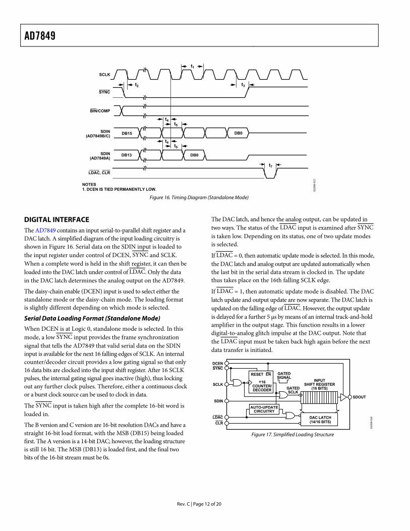
DIGITAL INTERFACE The AD7849 contains an input serial-to-parallel shift register and a DAC latch. A simplified diagram of the input loading circuitry is shown in Figure 16. Serial data on the SDIN input is loaded to the input register under control of DCEN, SYNC and SCLK. When a complete word is held in the shift register, it can then be loaded into the DAC latch under control of LDAC. Only the data in the DAC latch determines the analog output on the . AD7849
The daisy-chain enable (DCEN) input is used to select either the standalone mode or the daisy-chain mode. The loading format is slightly different depending on which mode is selected.
Serial Data Loading Format (Standalone Mode)
When DCEN is at Logic 0, standalone mode is selected. In this mode, a low SYNC input provides the frame synchronization signal that tells the that valid serial data on the SDIN input is available for the next 16 falling edges of SCLK. An internal counter/decoder circuit provides a low gating signal so that only 16 data bits are clocked into the input shift register. After 16 SCLK pulses, the internal gating signal goes inactive (high), thus locking out any further clock pulses. Therefore, either a continuous clock or a burst clock source can be used to clock in data.
AD7849
The SYNC input is taken high after the complete 16-bit word is loaded in.
The B version and C version are 16-bit resolution DACs and have a straight 16-bit load format, with the MSB (DB15) being loaded first. The A version is a 14-bit DAC; however, the loading structure is still 16 bit. The MSB (DB13) is loaded first, and the final two bits of the 16-bit stream must be 0s.
The DAC latch, and hence the analog output, can be updated in two ways. The status of the LDAC input is examined after SYNC is taken low. Depending on its status, one of two update modes is selected.
If LDAC = 0, then automatic update mode is selected. In this mode, the DAC latch and analog output are updated automatically when the last bit in the serial data stream is clocked in. The update thus takes place on the 16th falling SCLK edge.
If LDAC = 1, then automatic update mode is disabled. The DAC latch update and output update are now separate. The DAC latch is updated on the falling edge of LDAC. However, the output update is delayed for a further 5 μs by means of an internal track-and-hold amplifier in the output stage. This function results in a lower digital-to-analog glitch impulse at the DAC output. Note that the LDAC input must be taken back high again before the next data transfer is initiated.
÷16COUNTER/DECODER
RESET EN GATEDSIGNAL
INPUTSHIFT REGISTER
(16 BITS)GATEDSCLK
SDOUT
DCENSYNC
SCLK
AUTO-UPDATECIRCUITRY
SDIN
DAC LATCH(14/16 BITS)
LDACCLR
0100
8-01
8
Figure 17. Simplified Loading Structure
AD7849
Rev. C | Page 13 of 20
t2
DB0 (N) DB15(N + 1)
DB0(N + 1)
DB0 (N)DB15 (N)
DB0 (N)DB13 (N) DB13(N + 1)
DB0(N + 1)
DB0 (N)DB13 (N)
t6
SCLK
SYNC
BIN/COMP
SDIN(AD7849B/C)
SDOUT(AD7849B/C)
SDIN(AD7849A)
SDOUT(AD7849A)
LDAC, CLR
NOTES1. DCEN IS TIED PERMANENTLY HIGH.
t7
DB15 (N)
t6
t1
t3
t4t5
t4t5
0100
8-01
9
Figure 18. Timing Diagram (Daisy-Chain Mode)
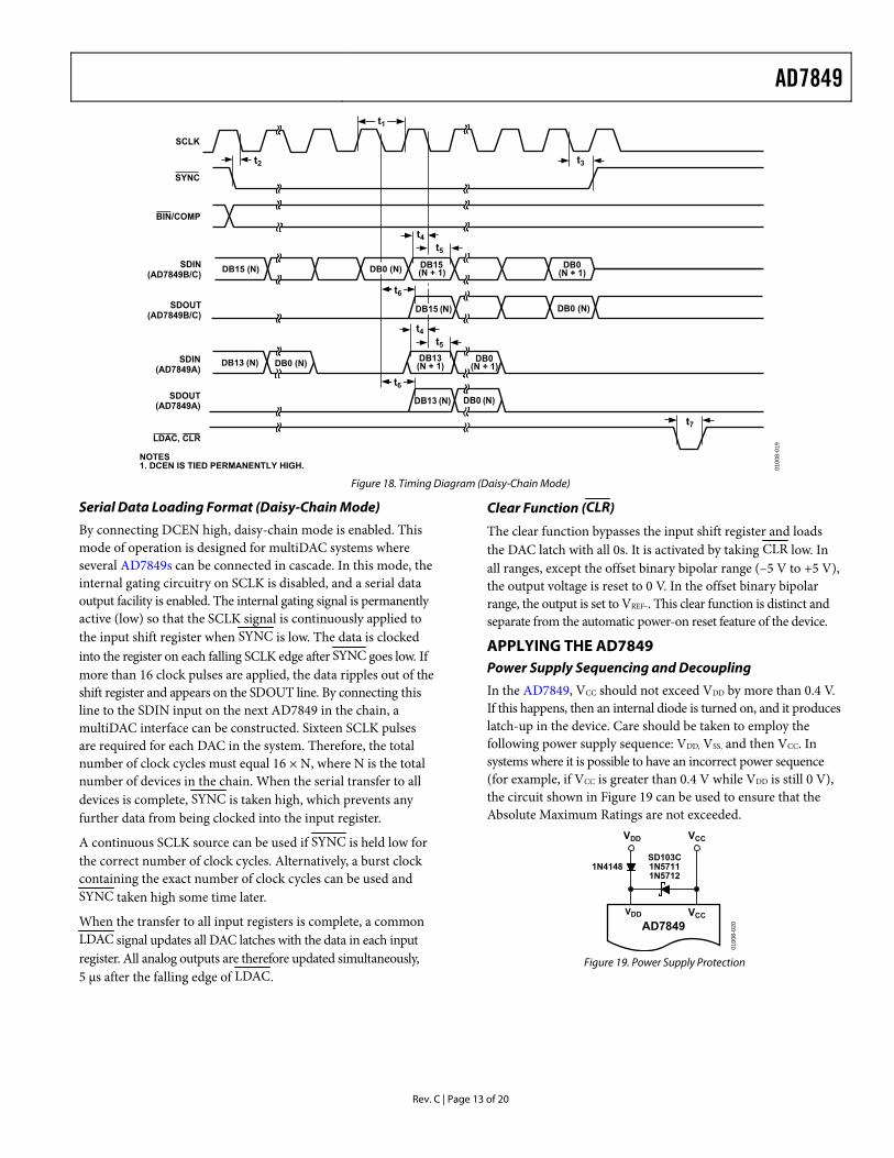
Serial Data Loading Format (Daisy-Chain Mode)
By connecting DCEN high, daisy-chain mode is enabled. This mode of operation is designed for multiDAC systems where several AD7849s can be connected in cascade. In this mode, the internal gating circuitry on SCLK is disabled, and a serial data output facility is enabled. The internal gating signal is permanently active (low) so that the SCLK signal is continuously applied to the input shift register when SYNC is low. The data is clocked into the register on each falling SCLK edge after SYNC goes low. If more than 16 clock pulses are applied, the data ripples out of the shift register and appears on the SDOUT line. By connecting this line to the SDIN input on the next in the chain, a multiDAC interface can be constructed. Sixteen SCLK pulses are required for each DAC in the system. Therefore, the total number of clock cycles must equal 16 × N, where N is the total number of devices in the chain. When the serial transfer to all devices is complete,
AD7849
SYNC is taken high, which prevents any further data from being clocked into the input register.
A continuous SCLK source can be used if SYNC is held low for the correct number of clock cycles. Alternatively, a burst clock containing the exact number of clock cycles can be used and SYNC taken high some time later.
When the transfer to all input registers is complete, a common LDAC signal updates all DAC latches with the data in each input register. All analog outputs are therefore updated simultaneously, 5 μs after the falling edge of LDAC.
Clear Function (CLR)
The clear function bypasses the input shift register and loads the DAC latch with all 0s. It is activated by taking CLR low. In all ranges, except the offset binary bipolar range (–5 V to +5 V), the output voltage is reset to 0 V. In the offset binary bipolar range, the output is set to VREF–. This clear function is distinct and separate from the automatic power-on reset feature of the device.
APPLYING THE AD7849 Power Supply Sequencing and Decoupling
In the AD7849, VCC should not exceed VDD by more than 0.4 V. If this happens, then an internal diode is turned on, and it produces latch-up in the device. Care should be taken to employ the following power supply sequence: VDD, VSS, and then VCC. In systems where it is possible to have an incorrect power sequence (for example, if VCC is greater than 0.4 V while VDD is still 0 V), the circuit shown in Figure 19 can be used to ensure that the Absolute Maximum Ratings are not exceeded.
SD103C1N57111N5712
1N4148
VDD VCC
VCCVDD
AD7849
0100
8-02
0
Figure 19. Power Supply Protection
AD7849
Rev. C | Page 14 of 20
Unipolar Configuration
Figure 20 shows the AD7849 in the unipolar binary circuit configuration. The DAC is driven by the AD586, 5 V reference. Because ROFS is tied to 0 V, the output amplifier has a gain of ×2, and the output range is 0 V to 10 V. If a 0 V to 5 V range is required, ROFS should be tied to VOUT, configuring the output stage for a gain of ×1. Table 7 gives the code table for the circuit shown in Figure 20.
ROFS
VDD VCC
VREF+
VOUTVOUT(0V TO 10V)
AGNDVREF–
VSS
–15V
AD7849*R110kΩ
AD586C1
1nF
SIGNAL GND
68
45
*ADDITIONAL PINS OMITTED FOR CLARITY.
2
DGND
+15V +5V
0100
8-02
1
Figure 20. Unipolar Binary Operation
Table 7. Code Table for Figure 20 Binary Number in DAC Latch MSB LSB Analog Output (VOUT) 1111 1111 1111 1111 10 (65,535/65,536) V 1000 0000 0000 0000 10 (32,768/65,536) V 0000 0000 0000 0001 10 (1/65,536) V 0000 0000 0000 0000 0 V
Table 7 assumes a 16-bit resolution; 1 LSB = 10 V/216 = 10 V/65,536 = 152 μV.
Offset and gain can be adjusted in Figure 20 as follows:
• To adjust offset, disconnect the VREF− input from 0 V, load the DAC with all 0s, and adjust the VREF− voltage until VOUT = 0 V.
• To adjust gain, load the AD7849 with all 1s and adjust R1 until VOUT = 10 (65,535/65,536) = 9.9998474 V for the 16-bit, B and C versions. For the 14-bit A version, VOUT should be 10 (16,383/16,384) = 9.9993896 V.
If a simple resistor divider is used to vary the VREF− voltage, it is important that the temperature coefficients of these resistors match that of the DAC input resistance (−300 ppm/°C). Otherwise, extra offset errors will be introduced over temperature. Many circuits do not require these offset and gain adjustments. In these circuits, R1 can be omitted. Pin 5 of the AD586 may be left open circuit, and Pin 2 (VREF−) of the AD7849 tied to 0 V.
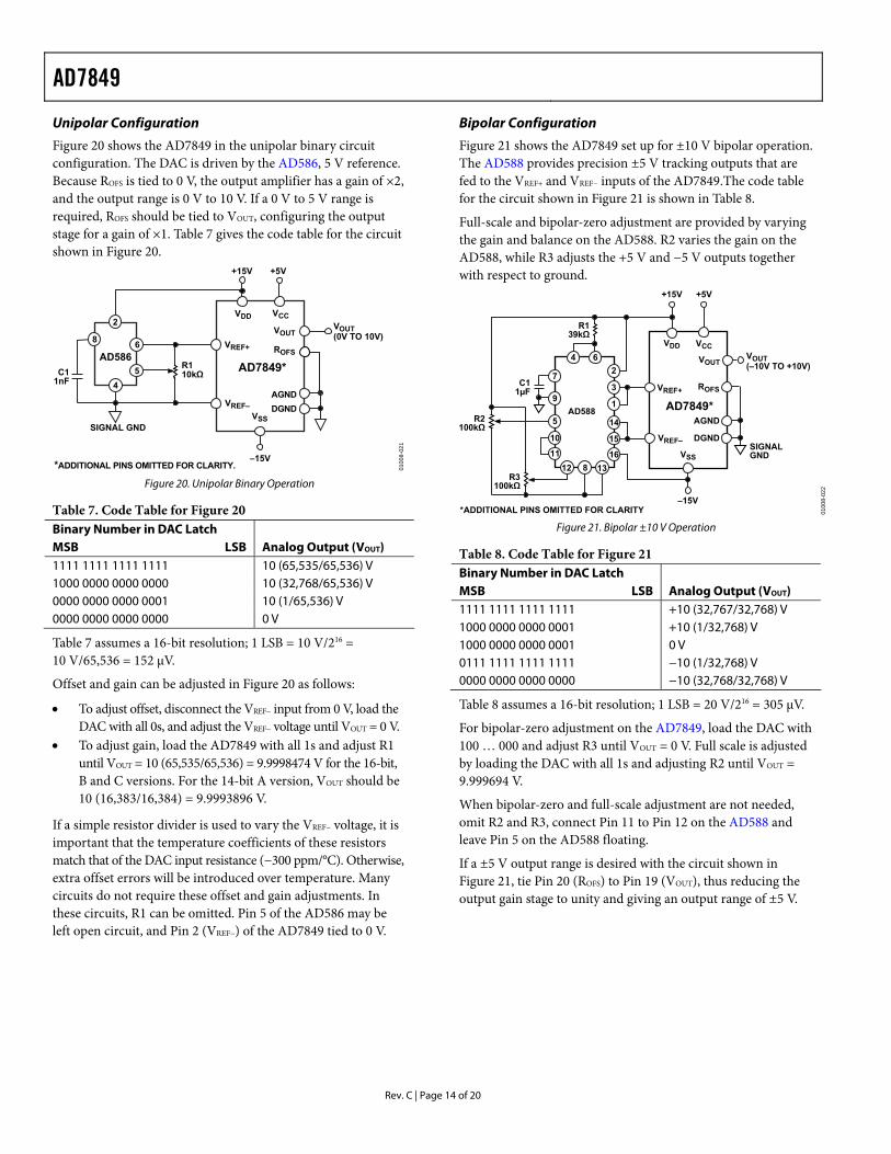
Bipolar Configuration
Figure 21 shows the AD7849 set up for ±10 V bipolar operation. The AD588 provides precision ±5 V tracking outputs that are fed to the VREF+ and VREF− inputs of the AD7849.The code table for the circuit shown in Figure 21 is shown in Table 8.
Full-scale and bipolar-zero adjustment are provided by varying the gain and balance on the AD588. R2 varies the gain on the AD588, while R3 adjusts the +5 V and −5 V outputs together with respect to ground.
VOUT(–10V TO +10V)
+15V +5V
VDD VCC
VREF+
VOUT
ROFS
AGND
DGNDVREF–
VSS
–15V
AD7849*
SIGNALGND
*ADDITIONAL PINS OMITTED FOR CLARITY
AD588
C11µF
R2100kΩ
R3100kΩ
R139kΩ
6
15
2
8
5 14
7
93
1
10
1211
4
1316
0100
8-02
2
Figure 21. Bipolar ±10 V Operation
Table 8. Code Table for Figure 21 Binary Number in DAC Latch MSB LSB Analog Output (VOUT) 1111 1111 1111 1111 +10 (32,767/32,768) V 1000 0000 0000 0001 +10 (1/32,768) V 1000 0000 0000 0001 0 V 0111 1111 1111 1111 −10 (1/32,768) V 0000 0000 0000 0000 −10 (32,768/32,768) V
Table 8 assumes a 16-bit resolution; 1 LSB = 20 V/216 = 305 μV.
For bipolar-zero adjustment on the AD7849, load the DAC with 100 … 000 and adjust R3 until VOUT = 0 V. Full scale is adjusted by loading the DAC with all 1s and adjusting R2 until VOUT = 9.999694 V.
When bipolar-zero and full-scale adjustment are not needed, omit R2 and R3, connect Pin 11 to Pin 12 on the AD588 and leave Pin 5 on the AD588 floating.
If a ±5 V output range is desired with the circuit shown in Figure 21, tie Pin 20 (ROFS) to Pin 19 (VOUT), thus reducing the output gain stage to unity and giving an output range of ±5 V.
AD7849
Rev. C | Page 15 of 20
Other Output Voltage Ranges
In some cases, users may require output voltage ranges other than those already mentioned. One example is systems that need the output voltage to be a whole number of millivolts (that is,1 mV or 2 mV). If the circuit shown in Figure 22 is used, then the LSB size is 125 μV. This makes it possible to program whole millivolt values at the output. Table 9 shows the code table for the circuit shown in Figure 22.
VDD VCC
VREF+VOUT
VOUT(0V TO 8.192V)
DGNDVREF–
AD7849*AD584
SIGNALGND
1
*ADDITIONAL PINS OMITTED FOR CLARITY.
8
4
ROFS
AGND
R2
R1 8.192V
+15V +5V
0100
8-02
3
Figure 22. 0 V to 8.192 V Output Range
Table 9. Code Table for Figure 22 Binary Number in DAC Latch MSB LSB Analog Output (VOUT) 1111 1111 1111 1111 8.192 V (65,535/65,536) = 8.1919 V 1000 0000 0000 0000 8.192 V (32,768/65,536) = 4.096 V 0000 0000 0000 1000 8.192 V (8/65,536) = 0.001 V 0000 0000 0000 0100 8.192 V (4/65,536) = 0.0005 V 0000 0000 0000 0010 8.192 V (2/65,536) = 0.00025 V 0000 0000 0000 0001 8.192 V (1/65,536) = 0.000125 V
Table 9 assumes a 16-bit resolution; 1 LSB = 8.192 V/216 = 125 μV.
Generating a ±5 V Output Range from a Single +5 V Reference
Figure 23 shows how to generate a ±5 V output range when using a single +5 V reference. VREF− is connected to 0 V, and ROFS is connected to VREF+. The 5 V reference input is applied to these pins. With all 0s loaded to the DAC, the noninverting terminal of the output stage amplifier is at 0 V, and VOUT is the inverse of VREF+. With all 1s loaded to the DAC, the noninverting terminal of the output stage amplifier is 5 V and, therefore, VOUT is also 5 V.
ROFS
VDD VCC
VREF+ VOUTVOUT(–5V TO +5V)
DGNDVREF–
VSS
–15V
AD7849*R110kΩ
AD586C1
1nF
SIGNAL GND
68
45
*ADDITIONAL PINS OMITTED FOR CLARITY.
2
AGND
+15V +5V
0100
8-02
4
Figure 23. Generating a ±5 V Output Range from a Single +5 V
MICROPROCESSOR INTERFACING Microprocessor interfacing to the AD7849 is via a serial bus that uses standard protocol compatible with DSP processors and microcontrollers. The communications channel requires a 3-wire interface consisting of a clock signal, a data signal, and a synchronization signal. The AD7849 requires a 16-bit data-word with data valid on the falling edge of SCLK. For all the interfaces, the DAC update can be done automatically when all data is clocked in, or it can be done under control of LDAC.
Figure 24 through Figure 27 show the AD7849 configured for interfacing to a number of popular DSP processors and microcontrollers.
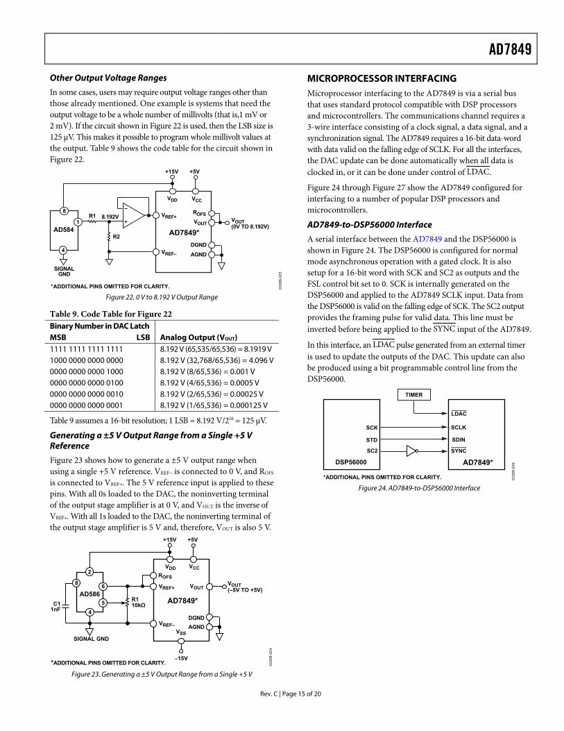
AD7849-to-DSP56000 Interface
A serial interface between the AD7849 and the DSP56000 is shown in Figure 24. The DSP56000 is configured for normal mode asynchronous operation with a gated clock. It is also setup for a 16-bit word with SCK and SC2 as outputs and the FSL control bit set to 0. SCK is internally generated on the DSP56000 and applied to the AD7849 SCLK input. Data from the DSP56000 is valid on the falling edge of SCK. The SC2 output provides the framing pulse for valid data. This line must be inverted before being applied to the SYNC input of the . AD7849
In this interface, an LDAC pulse generated from an external timer is used to update the outputs of the DAC. This update can also be produced using a bit programmable control line from the DSP56000.
DSP56000
SCK
STD
SC2
AD7849*
LDAC
SCLK
SDIN
SYNC
*ADDITIONAL PINS OMITTED FOR CLARITY.
TIMER
0100
8-02
9
Figure 24. AD7849-to-DSP56000 Interface
AD7849
Rev. C | Page 16 of 20
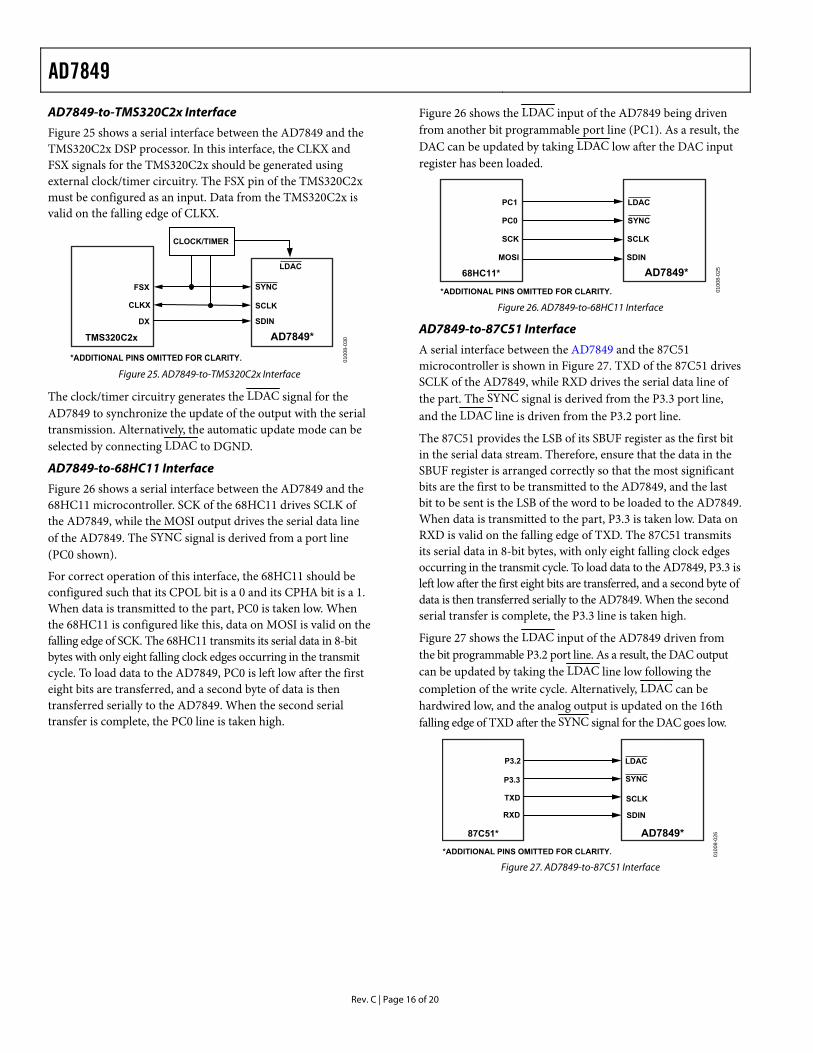
Figure 26 shows the LDAC input of the being driven from another bit programmable port line (PC1). As a result, the DAC can be updated by taking
AD7849
LDAC low after the DAC input register has been loaded.
AD7849-to-TMS320C2x Interface
Figure 25 shows a serial interface between the AD7849 and the TMS320C2x DSP processor. In this interface, the CLKX and FSX signals for the TMS320C2x should be generated using external clock/timer circuitry. The FSX pin of the TMS320C2x must be configured as an input. Data from the TMS320C2x is valid on the falling edge of CLKX.
68HC11*
PC0
SCK
MOSI
PC1
AD7849*
LDAC
SCLK
SDIN
SYNC
*ADDITIONAL PINS OMITTED FOR CLARITY. 0100
8-02
5
TMS320C2x
FSX
CLKX
DX
AD7849*
LDAC
SCLK
SDIN
SYNC
*ADDITIONAL PINS OMITTED FOR CLARITY.
CLOCK/TIMER
0100
8-03
0
Figure 26. AD7849-to-68HC11 Interface
AD7849-to-87C51 Interface
A serial interface between the AD7849 and the 87C51 microcontroller is shown in Figure 27. TXD of the 87C51 drives SCLK of the AD7849, while RXD drives the serial data line of the part. The SYNC signal is derived from the P3.3 port line, and the LDAC line is driven from the P3.2 port line.
Figure 25. AD7849-to-TMS320C2x Interface
The clock/timer circuitry generates the LDAC signal for the to synchronize the update of the output with the serial
transmission. Alternatively, the automatic update mode can be selected by connecting
AD7849
LDAC to DGND. The 87C51 provides the LSB of its SBUF register as the first bit in the serial data stream. Therefore, ensure that the data in the SBUF register is arranged correctly so that the most significant bits are the first to be transmitted to the AD7849, and the last bit to be sent is the LSB of the word to be loaded to the AD7849. When data is transmitted to the part, P3.3 is taken low. Data on RXD is valid on the falling edge of TXD. The 87C51 transmits its serial data in 8-bit bytes, with only eight falling clock edges occurring in the transmit cycle. To load data to the AD7849, P3.3 is left low after the first eight bits are transferred, and a second byte of data is then transferred serially to the AD7849. When the second serial transfer is complete, the P3.3 line is taken high.
AD7849-to-68HC11 Interface
Figure 26 shows a serial interface between the AD7849 and the 68HC11 microcontroller. SCK of the 68HC11 drives SCLK of the AD7849, while the MOSI output drives the serial data line of the AD7849. The SYNC signal is derived from a port line (PC0 shown).
For correct operation of this interface, the 68HC11 should be configured such that its CPOL bit is a 0 and its CPHA bit is a 1. When data is transmitted to the part, PC0 is taken low. When the 68HC11 is configured like this, data on MOSI is valid on the falling edge of SCK. The 68HC11 transmits its serial data in 8-bit bytes with only eight falling clock edges occurring in the transmit cycle. To load data to the AD7849, PC0 is left low after the first eight bits are transferred, and a second byte of data is then transferred serially to the AD7849. When the second serial transfer is complete, the PC0 line is taken high.
Figure 27 shows the LDAC input of the driven from the bit programmable P3.2 port line. As a result, the DAC output can be updated by taking the
AD7849
LDAC line low following the completion of the write cycle. Alternatively, LDAC can be hardwired low, and the analog output is updated on the 16th falling edge of TXD after the SYNC signal for the DAC goes low.
87C51*
P3.3
TXD
RXD
P3.2
AD7849*
LDAC
SCLK
SDIN
SYNC
*ADDITIONAL PINS OMITTED FOR CLARITY. 0100
8-02
6
Figure 27. AD7849-to-87C51 Interface
AD7849
Rev. C | Page 17 of 20
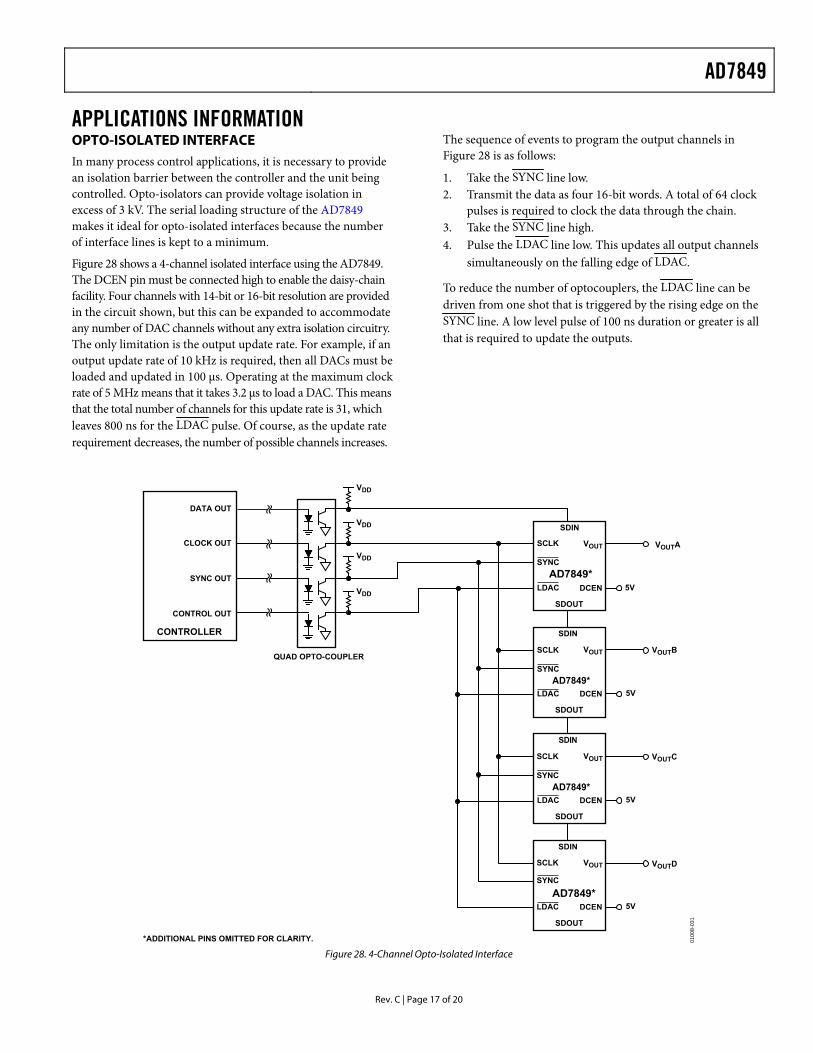
APPLICATIONS INFORMATION OPTO-ISOLATED INTERFACE In many process control applications, it is necessary to provide an isolation barrier between the controller and the unit being controlled. Opto-isolators can provide voltage isolation in excess of 3 kV. The serial loading structure of the AD7849 makes it ideal for opto-isolated interfaces because the number of interface lines is kept to a minimum.
Figure 28 shows a 4-channel isolated interface using the AD7849. The DCEN pin must be connected high to enable the daisy-chain facility. Four channels with 14-bit or 16-bit resolution are provided in the circuit shown, but this can be expanded to accommodate any number of DAC channels without any extra isolation circuitry. The only limitation is the output update rate. For example, if an output update rate of 10 kHz is required, then all DACs must be loaded and updated in 100 μs. Operating at the maximum clock rate of 5 MHz means that it takes 3.2 μs to load a DAC. This means that the total number of channels for this update rate is 31, which leaves 800 ns for the LDAC pulse. Of course, as the update rate requirement decreases, the number of possible channels increases.
The sequence of events to program the output channels in Figure 28 is as follows:
1. Take the SYNC line low. 2. Transmit the data as four 16-bit words. A total of 64 clock
pulses is required to clock the data through the chain. 3. Take the SYNC line high. 4. Pulse the LDAC line low. This updates all output channels
simultaneously on the falling edge of LDAC.
To reduce the number of optocouplers, the LDAC line can be driven from one shot that is triggered by the rising edge on the SYNC line. A low level pulse of 100 ns duration or greater is all that is required to update the outputs.
VDD
VDD
VDD
VDD
DATA OUT
CLOCK OUT
SYNC OUT
CONTROL OUT
CONTROLLER
VOUTA
VOUTB
VOUTC
VOUTD
5V
QUAD OPTO-COUPLER
*ADDITIONAL PINS OMITTED FOR CLARITY.
LDAC
SDIN
VOUT
DCEN
SDOUT
AD7849*
5VLDAC
SDIN
VOUT
DCEN
SDOUT
AD7849*
5VLDAC
SDIN
VOUT
DCEN
SDOUT
AD7849*
5V
SCLK
SYNC
LDAC
SDIN
VOUT
DCEN
SDOUT
AD7849*
0100
8-03
1
SCLK
SYNC
SCLK
SYNC
SCLK
SYNC
Figure 28. 4-Channel Opto-Isolated Interface
AD7849
Rev. C | Page 18 of 20
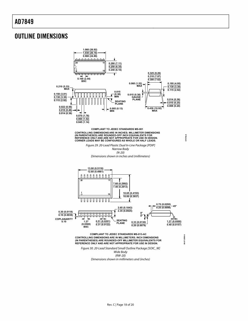
OUTLINE DIMENSIONS
CONTROLLING DIMENSIONS ARE IN INCHES; MILLIMETER DIMENSIONS(IN PARENTHESES) ARE ROUNDED-OFF INCH EQUIVALENTS FORREFERENCE ONLY AND ARE NOT APPROPRIATE FOR USE IN DESIGN.CORNER LEADS MAY BE CONFIGURED AS WHOLE OR HALF LEADS.
COMPLIANT TO JEDEC STANDARDS MS-001
0707
06-A
0.022 (0.56)0.018 (0.46)0.014 (0.36)
0.150 (3.81)0.130 (3.30)0.115 (2.92)
0.070 (1.78)0.060 (1.52)0.045 (1.14)
20
110
11
0.100 (2.54)BSC
1.060 (26.92)1.030 (26.16)0.980 (24.89)
0.210 (5.33)MAX
SEATINGPLANE
0.015(0.38)MIN
0.005 (0.13)MIN
0.280 (7.11)0.250 (6.35)0.240 (6.10)
0.060 (1.52)MAX
0.430 (10.92)MAX
0.014 (0.36)0.010 (0.25)0.008 (0.20)
0.325 (8.26)0.310 (7.87)0.300 (7.62)
0.015 (0.38)GAUGEPLANE
0.195 (4.95)0.130 (3.30)0.115 (2.92)
Figure 29. 20-Lead Plastic Dual In-Line Package [PDIP]
Narrow Body (N-20)
Dimensions shown in inches and (millimeters)
CONTROLLING DIMENSIONS ARE IN MILLIMETERS; INCH DIMENSIONS(IN PARENTHESES) ARE ROUNDED-OFF MILLIMETER EQUIVALENTS FORREFERENCE ONLY AND ARE NOT APPROPRIATE FOR USE IN DESIGN.
COMPLIANT TO JEDEC STANDARDS MS-013-AC
13.00 (0.5118)12.60 (0.4961)
0.30 (0.0118)0.10 (0.0039)
2.65 (0.1043)2.35 (0.0925)
10.65 (0.4193)10.00 (0.3937)
7.60 (0.2992)7.40 (0.2913)
0.75 (0.0295)0.25 (0.0098) 45°
1.27 (0.0500)0.40 (0.0157)
COPLANARITY0.10 0.33 (0.0130)
0.20 (0.0079)0.51 (0.0201)0.31 (0.0122)
SEATINGPLANE
8°0°
20 11
101
1.27(0.0500)
BSC
06-0
7-20
06-A
Figure 30. 20-Lead Standard Small Outline Package [SOIC_W]
Wide Body (RW-20)
Dimensions shown in millimeters and (inches)
AD7849
Rev. C | Page 19 of 20
ORDERING GUIDE Model1 Temperature Range Resolution (Bits) Bipolar INL (LSB) Package Description Package Option AD7849ANZ −40°C to +85°C 14 ±3 20-Lead PDIP N-20 AD7849BNZ −40°C to +85°C 16 ±8 20-Lead PDIP N-20 AD7849CNZ −40°C to +85°C 16 ±4 20-Lead PDIP N-20 AD7849AR −40°C to +85°C 14 ±3 20-Lead SOIC_W RW-20 AD7849AR-REEL −40°C to +85°C 14 ±3 20-Lead SOIC_W RW-20 AD7849ARZ −40°C to +85°C 14 ±3 20-Lead SOIC_W RW-20 AD7849ARZ-REEL −40°C to +85°C 14 ±3 20-Lead SOIC_W RW-20 AD7849BR −40°C to +85°C 16 ±8 20-Lead SOIC_W RW-20 AD7849BR-REEL −40°C to +85°C 16 ±8 20-Lead SOIC_W RW-20 AD7849BRZ −40°C to +85°C 16 ±8 20-Lead SOIC_W RW-20 AD7849BRZ-REEL −40°C to +85°C 16 ±8 20-Lead SOIC_W RW-20 AD7849CR −40°C to +85°C 16 ±4 20-Lead SOIC_W RW-20 AD7849CR-REEL −40°C to +85°C 16 ±4 20-Lead SOIC_W RW-20 AD7849CRZ −40°C to +85°C 16 ±4 20-Lead SOIC_W RW-20 AD7849CRZ-REEL −40°C to +85°C 16 ±4 20-Lead SOIC_W RW-20 1 Z = RoHS Compliant Part.
AD7849
Rev. C | Page 20 of 20
NOTES
©1995–2011 Analog Devices, Inc. All rights reserved. Trademarks and registered trademarks are the property of their respective owners. D01008-0-3/11(C)