Embed Size (px)
Citation preview
This content has been downloaded from IOPscience. Please scroll down to see the full text.
Download details:
IP Address: 128.83.63.20
This content was downloaded on 28/09/2014 at 13:05
Please note that terms and conditions apply.
Internal quantum efficiency analysis of plasmonic textured silicon solar cells: surface plasmon
resonance and off-resonance effects
View the table of contents for this issue, or go to the journal homepage for more
2014 J. Phys. D: Appl. Phys. 47 425101
(http://iopscience.iop.org/0022-3727/47/42/425101)
Home Search Collections Journals About Contact us My IOPscience

Journal of Physics D: Applied Physics
J. Phys. D: Appl. Phys. 47 (2014) 425101 (7pp) doi:10.1088/0022-3727/47/42/425101
Internal quantum efficiency analysis ofplasmonic textured silicon solar cells:surface plasmon resonance andoff-resonance effectsEshwar Thouti1, Ashok K Sharma2, Sanjay K Sardana1
and Vamsi K Komarala1
1 Centre for Energy Studies, Indian Institute of Technology Delhi, New Delhi-110016, India2 Department of Electrical Engineering, Indian Institute of Technology Bombay, Mumbai-400076, India
E-mail: [email protected] and [email protected]
Received 5 June 2014, revised 14 August 2014Accepted for publication 22 August 2014Published 18 September 2014
AbstractSilver nanoparticles (Ag NPs) of various sizes and concentration were integrated on texturedsilicon solar cells for further confinement of incident light, generated photocurrentmodifications were investigated using spectrally resolved short-circuit current measurements.Internal quantum efficiency (IQE) spectra were used for quantifying the effective minoritycarrier diffusion lengths (Leff) of plasmonic cells in the long wavelength region(850 < λ < 1020 nm). The Leff of an optimized plasmonic solar cell enhanced to 431 µmcompared to 338 µm of the bare cell, which is due to interacting Ag NPs’ scattered fields,leading to enhanced light absorption in the plasmonic cell. Despite the enhanced Leff values,the overall generated photocurrent reduced with Ag NPs which is due to the significant lossesnear the surface plasmon resonant region. Reduced IQE of plasmonic cells near and below thesurface plasmon resonant region is due to size-dependent parasitic absorption and enhancedback scattering of Ag NPs, and a modified surface recombination process due to Ag NPs’strong near-fields.
Keywords: plasmonics, textured silicon solar cell, internal quantum efficiency, minority carrierdiffusion length
(Some figures may appear in colour only in the online journal)
1. Introduction
Recently, the integration of plasmonics concepts in siliconsolar cell structure have proved to be essential for reducingmaterial thickness and for improving the efficiencies further[1, 2]. The optical nanoscience, also called plasmonics, is oneof the leading areas in the nano-photonics field. Plasmonicsbased applications are vast and growing day by day in variousscientific fields; reason being light folding/slowing is possibleat the nanoscale after interaction with free electrons of metalnanoparticles (NPs). The incident light can either be absorbedor scattered more than the geometric size of NPs depending onthe size, shape and dielectric environment of metal NPs [3]; this
enhanced absorption/scattering phenomenon can be exploitedin organic/inorganic solar cells.
Since the pioneering work of Stuart and Hall on plasmonicsilicon on insulator photodetectors [4], the integration of metalnanostructures in photonic devices has become a scientificcuriosity [5–9]. Silver (Ag) NPs are proven to be superiorover gold (Au) NPs for front side integration with photovoltaiccells due to their high radiative efficiency and occurrence ofinterband transitions at short wavelengths. Researchers havebeen using optimized Ag NPs on front side of silicon solar cellin order to utilize their scattering properties [6–8]. One of themotivations behind the integration of metal nanostructures insilicon solar cells is to harness near band gap long wavelength
0022-3727/14/425101+07$33.00 1 © 2014 IOP Publishing Ltd Printed in the UK
J. Phys. D: Appl. Phys. 47 (2014) 425101 E Thouti et al
photons by enhancing their optical path length further withthe help of scattered fields of metal nanostructures, apart fromthe conventional texturization and anti-reflection coatings foradditional power generating electrons in silicon layer.
In this work, we have tried to understand the opticaland electronic properties of textured silicon (T–Si) solar cellsintegrated with Ag NPs of various sizes and concentrations.Our main aim of this study is to find out how the minoritycarrier diffusion lengths in the base region of the T–Si cellwould be affected due to the presence of plasmon fields of AgNPs. Here, we have analysed the effective minority carrierdiffusion lengths from the internal quantum efficiency (IQE)measurements of plasmonic T–Si solar cells. For this purpose,we have used simple physical vapour deposition techniquefor synthesizing Ag NPs of various sizes and concentrations.Quantum efficiency measurements were performed to observethe surface plasmon resonance and off-resonance effects of AgNPs on incident photon to photoelectron conversion.
2. Experimental methods
Textured silicon solar cells used for these experiments werefabricated via conventional in line process. Briefly; P-typeCzochralski grown silicon ((1 0 0) oriented) wafers havingthickness of 200 ± 10 µm and resistivity in the rage of0.5–3 � cm were used as a starting material for the cellfabrication. After the saw damage removal using an alkalinechemical (NaOH, 40% vol/vol, @80 ◦C for 30 s), alkalinetexturization was done at standard etch conditions (NaOH,4% vol/vol, @85 ◦C for 15 min). Consecutively, a shallow∼0.3 µm n-type layer was grown on textured wafers usingPOCl3 diffusion at 880 ◦C for 40 min. The dead layer orphosphosilicate glass was removed using buffered HF (10% HFfor 2 min) followed by a plasma based edge isolation. Silverand aluminum materials were screen printed on front and rearsides of the p–n junction, respectively. Finally, co-firing wasdone to form ohmic contacts on both sides, as well as backsurface field at the rear side of the cell. An anti-reflectioncoating step was avoided. For the experimental purpose,∼2 cm2area T–Si cells were used by cutting from the standardcell size of 5 inch × 5 inch. After cutting, cells were annealedat 400 ◦C for 1 h in the nitrogen ambient in order to avoid anymodifications associated during the Ag NPs preparation onT–Si surface. The Ag films with mass thickness of ∼1 nm,3 nm, 5 nm, 10 nm and 15 nm were deposited by a thermalevaporation technique. The films were subsequently annealedat temperatures of 300 and 400 ◦C for 1 h in the nitrogenambient, which resulted in the formation of Ag NPs of varioussizes and concentrations. The T–Si cells integrated with Agmass thickness of ∼1 nm, 3 nm, 5 nm, 10 nm and 15 nm havebeen named as C1, C3, C5, C10 and C15, respectively, and thebare T–Si cell (reference cell) has been named as C0.
Surface morphological studies of Ag NPs were carriedout using a Carl Zeiss scanning electron microscope. SilverNP size distribution was analysed using the UTHSCSAImage Tool program [10]. Current density–voltage (J–V ) characteristics of solar cells were carried out under thestandard test conditions (Room temperature and AM1.5G
spectrum) using Oriel class AAA solar simulator (Oriel Sol3A,Newport, USA). A Keithley 2440 source-meter was used forthe J–V measurements. External Quantum efficiency andtotal reflectance spectra were recorded at room temperatureusing SpeQuest quantum efficiency measurement system fromReRa Solutions, Netherlands. Total reflectance spectra of aT–Si cell with and without Ag NPs were measured using a30 mm integrating sphere attached to the quantum efficiencymeasurement setup. The external quantum efficiency (EQE)and the total reflectance (TR) spectra were used for calculatingthe IQE of all T–Si cells. The incident light beam spot sizewas ∼3 mm for the EQE and total reflectance measurements.Measurements were performed at different positions of theplasmonic T–Si cell in order to observe any variations in therecorded EQE and TR spectra which might have occurred dueto any spatial variations in the size and concentration of AgNPs. However, we found negligible variation in the recordedspectra, allowing us to conclude that NPs formation is nearlyuniform over ∼2 cm2 area of T–Si cells.
3. Results and discussions
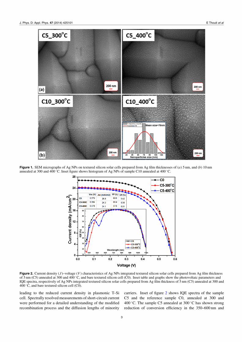
Morphological variations of Ag NPs on T–Si cells are achievedby annealing the samples C1, C3, C5, C10 and C15 at 300 and400 ◦C. Figure 1 shows the surface morphology of samples C5and C10. The film thickness plays a major role in determiningthe NPs size, apart from annealing temperatures. Initialannealing of samples at 300 ◦C led to the formation of smallersized NPs with a high density (figure 1(a)). An increase ofannealing temperature to 400 ◦C led to an increase in NPs sizeswith reduced surface coverage (figure 1(b), it is clearly visibleonly for large film thicknesses). This is due to the high atomicdiffusion at higher temperatures which leads to aggregationand formation of larger particles because the surface tensionof particles gets minimized [11, 12]. It is difficult to quantifythe size and percentage of Ag NPs coverage on the T–Sisurface after 300 ◦C annealing temperature due to large surfacecoverage. However, we were able to measure the size of NPsafter 400 ◦C annealing of samples C10 and C15 using ImageTool software. For lower Ag mass thicknesses (C1, C3 andC5), it is difficult to distinguish Ag NPs even after the annealingat 400 ◦C. For higher Ag mass thicknesses (C10 and C15), anincrease in particle sizes (see inset of figure1(b), in the case ofC10 average size ∼76 nm) is observed after the annealing at400 ◦C.
Current density–voltage characteristics of all T–Si cellsamples were measured without and with Ag NPs afterannealing at 300 and 400 ◦C. Figure 2 presents the J–V curvesof the C5 sample; from the figure we can see the slightlyreduced photocurrent with Ag NPs prepared at 300 ◦C whichis due to the recombination of some electron–hole pairs thatdo not contribute to the electric current. On increasing theannealing temperature further to 400 ◦C, the current density isnot affected much but the reduction in fill factor (Inset table)is observed. The observed trends in J–V curves of all thesamples were similar to sample C5, with varying magnitudesof parameters (not shown here). From J–V curves, we cannotunderstand the location of increased carrier recombination
2
J. Phys. D: Appl. Phys. 47 (2014) 425101 E Thouti et al
Figure 1. SEM micrographs of Ag NPs on textured silicon solar cells prepared from Ag film thicknesses of (a) 5 nm, and (b) 10 nmannealed at 300 and 400 ◦C. Inset figure shows histogram of Ag NPs of sample C10 annealed at 400 ◦C.
Figure 2. Current density (J )–voltage (V ) characteristics of Ag NPs integrated textured silicon solar cells prepared from Ag film thicknessof 5 nm (C5) annealed at 300 and 400 ◦C, and bare textured silicon cell (C0). Inset table and graphs show the photovoltaic parameters andIQE spectra, respectively of Ag NPs integrated textured silicon solar cells prepared from Ag film thickness of 5 nm (C5) annealed at 300 and400 ◦C, and bare textured silicon cell (C0).
leading to the reduced current density in plasmonic T–Sicell. Spectrally resolved measurements of short-circuit currentwere performed for a detailed understanding of the modifiedrecombination process and the diffusion lengths of minority
carriers. Inset of figure 2 shows IQE spectra of the sampleC5 and the reference sample C0, annealed at 300 and400 ◦C. The sample C5 annealed at 300 ◦C has shown strongreduction of conversion efficiency in the 350–600 nm and
3

J. Phys. D: Appl. Phys. 47 (2014) 425101 E Thouti et al
Figure 3. IQE and total reflectance spectra of textured silicon solar cells without (C0) and with Ag NPs prepared from Ag film thicknessesof ∼3, 5, 10 and 15 nm, annealed at (a) 300 ◦C, and (b) 400 ◦C. Inset shows relative IQE enhancements of corresponding samples.
slight enhancement in the 800–1100 nm wavelength regions,which resulted in an overall reduction of current densityby ∼2.5 mA cm−2 compared to the sample C0 (Inset table).After annealing at 400 ◦C, the IQE spectrum recovers to thebaseline value between 350 to 460 nm region, but there is astrong reduction near the surface plasmon resonance region(with the valley at 520 nm). The small enhancement from800 to 1100 nm region is still present. The decrement incurrent density is nearly same (inset table in figure 1) for thetwo annealing temperatures, which is due to the wavelengthdependent modification of IQE near the surface plasmonresonant region. From these observations we can infer thatthe reduction of IQE is very sensitive to the variations inparticle sizes and concentrations near the surface plasmonresonance region. On the contrary, the off-resonant region(800–1100 nm) appears to be insensitive to these variations.
In figure 3, we have presented the IQE and total reflectancespectra of samples C0, C3, C5, C10 and C15 annealed at 300and 400 ◦C in order to see the Ag mass thickness dependenceon opto-elctronic properties. When the samples are annealedat 300 ◦C (figure 3(a)), the small Ag film thickness samples C3and C5 show a small reduced TR in the entire polychromaticspectrum. On the other hand, the large Ag film thicknesssamples C10 and C15 show increased TR near the surfaceplasmon resonant region in spite of a small reduction inreflectance in the off-resonant region, as compared to thesample C0. Samples C3 and C5 show a small enhancement
of IQE in the off-resonant surface plasmon region due to thereduced reflectance. But the reduced reflectance near theplasmon resonant region results in IQE reduction instead ofenhancement, compared to the reference sample C0. In thecase of samples C10 and C15, the IQE is substantially reducednear the resonant region. However, a small enhancementis observed in the off-resonant region for the sample C10,while the sample C15 does not show an appreciable changein this region. When we increase the annealing temperatureto 400 ◦C (figure 3(b)), the TR of all the samples is increasednear the resonance region except for sample C3 [8, 11]. Butthe TR of all the samples is slightly less than the sampleC0 in the off-resonant region. The increase in TR (peakposition and broadness) is very sensitive to the initial Ag filmthickness. Thus, the IQE spectrum valley and the reflectancepeak positions are red-shifted (from 500 nm to 550 nm forC10, and 500 nm to 590 for C15 samples) after annealingthe samples at 400 ◦C when compared to 300 ◦C. The IQEof samples C3, C5 and C10 is slightly enhanced in the off-resonant region with the 400 ◦C annealing, however, there isa strong reduction near the surface plasmon resonance region[8, 13]. In the long wavelength region (800–1100 nm), relativeIQE enhancements of all the samples annealed at 300 and400 ◦C can be seen in insets of figures 3(a) and (b).
The IQE analysis clearly shows that the light generatedphotocurrent is wavelength dependent and non-uniform innature. The contributing factors to the observed Ag film
4
J. Phys. D: Appl. Phys. 47 (2014) 425101 E Thouti et al
thickness dependent IQE spectra are; (1) size-dependent AgNPs parasitic absorption; which is an unavoidable issue due tonon-negligible value of imaginary part of dielectric constantof metal NPs in the visible region. (2) The modification ofminority carrier recombination process due to the near andfar-fields of surface plasmons excited on Ag NPs. Lightabsorption is desirable in silicon material but not in Ag NPs.But, the strong reduction of IQE near the surface plasmonresonance region is due to the parasitic absorption by the AgNPs, where the incident light is converted into near-fieldsand finally dissipated as heat. Sometimes strong absorptionin NPs can also take place due to the polycrystalline natureof NPs, since the collective oscillating electrons near thesurface plasmon resonance lose their energy while interactingwith grain boundaries, defects and surface roughness [14].After increasing the annealing temperature of sample C5 to400 ◦C, along with the parasitic absorption the back scatteringcomponent also showed an increment, which resulted in anincreased reflectance. At the resonant wavelengths, peakedoscillation of electron cloud can lead to maximum absorptionand/or scattering. Apart from the absorption, the exciteddipolar resonances show an equal probability for forwardand backward scattering when the NPs are embedded in ahomogeneous medium. However, the forward and backwardscattering efficiencies will be modified if the NPs are placedat the interface between two mediums of different permittivity[3, 15, 16].
Whatever modifications (by Ag NPs) on the front surfaceof a cell we have, they seem to alter both its optical as wellas the electronic properties; thus, they function in much thesame manner as surface texturization. Reflectance from thesurface can be reduced with the texturization, but the surfacerecombination process will be enhanced due to an increasein the number of surface defect states. An IQE spectrumis a contribution from the three regions of a p–n junctionsilicon solar cell, namely the emitter, space charge and base[17]. Light radiation with wavelengths less than 500 nm canpenetrate only up to a few hundreds of nanometres into thesilicon cell due to a large absorption coefficient and theyalso have maximum intensity in the incident polychromaticsolar spectrum. This leads to generation of maximumnumber of charge carriers in the emitter and close to the p–njunction regions. Front surface recombination is a well-knowndetrimental factor in silicon solar cells. It has a strong influenceon the collection probability of generated carriers in the shortwavelength region. Initial annealing at lower temperature(300 ◦C) leads to the formation of highly dense NPs, whichmight have a large contact area between the NPs and the emittersurface. The strong near-fields produced by Ag NPs can reducethe optical absorption depth by generating maximum numberof electron–hole pairs on the front surface of the cell [18].Thus, there is a possibility for large surface recombinationwith low collection probability. The significant observation inour study is the restoration of the reduced IQE spectra in the350–500 nm wavelength region with the increase in annealingtemperature from 300 to 400 ◦C, which gives an idea that thefront surface recombination is reduced. Annealing of samplesat higher temperature (400 ◦C) may lead to the formation of
nearly spherical NPs with a reduced contact area. This reducedcontact area (reduced near-fields) might have little effect onsurface recombination and collection probability. Also, theT–Si cells used in our experiments do not have an anti-reflectioncoating, which usually passivates some of the surface defectstates and can also act as a barrier/spacer layer for the strongnear-fields generated at the interface due to the presence ofAg NPs.
To some extent, the off-resonant region (λ ∼ 800–1100 nm) of surface plasmons show forward scattering whichis clearly evident from the slight enhancement of IQE(figure 3). Long wavelength light (λ > 800 nm) can penetrateinto the entire silicon material due to its smaller absorptioncoefficient. So, for wavelengths above 800 nm the contributionto IQE is from the base region. The detailed analysis of IQEof a solar cell will give an approximate idea about effectivediffusion lengths of minority carriers (Leff) near the bandgapregion (from 850 to 1050 nm) of silicon [19]. Here, we tryto quantify the diffusion length of minority carriers for allthe cells in the near bandgap wavelengths using the followingequation [20, 21].
IQE−1 = 1 +Lα
Leffcos θ, (1)
where α is the absorption coefficient of silicon, Lα is theoptical absorption length, Leff is the effective diffusion lengthsof minority carriers, cosθ accounts for the light path lengthenhancement in the textured silicon cell, and θ = 41.8◦ takenfor textured silicon as it is the angle between the texturedsurface and the light penetrating into the cell [21]. Absorptioncoefficient data for silicon in the broad wavelengths has beentaken from Green et al [22] for calculations. In the presentcase, near band gap wavelengths account for the off-resonantregion of IQE spectra of T–Si cells integrated with Ag NPs.Hence, it is possible to study how the Leff is being modifiedafter the integration of NPs.
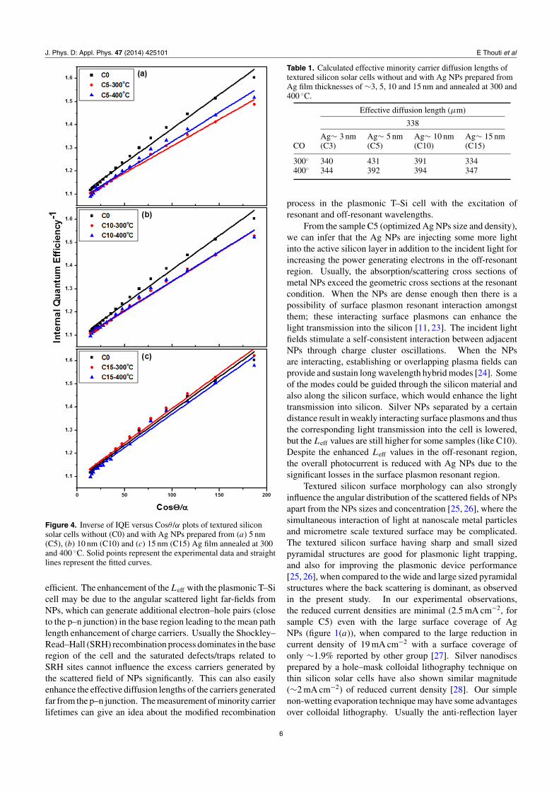
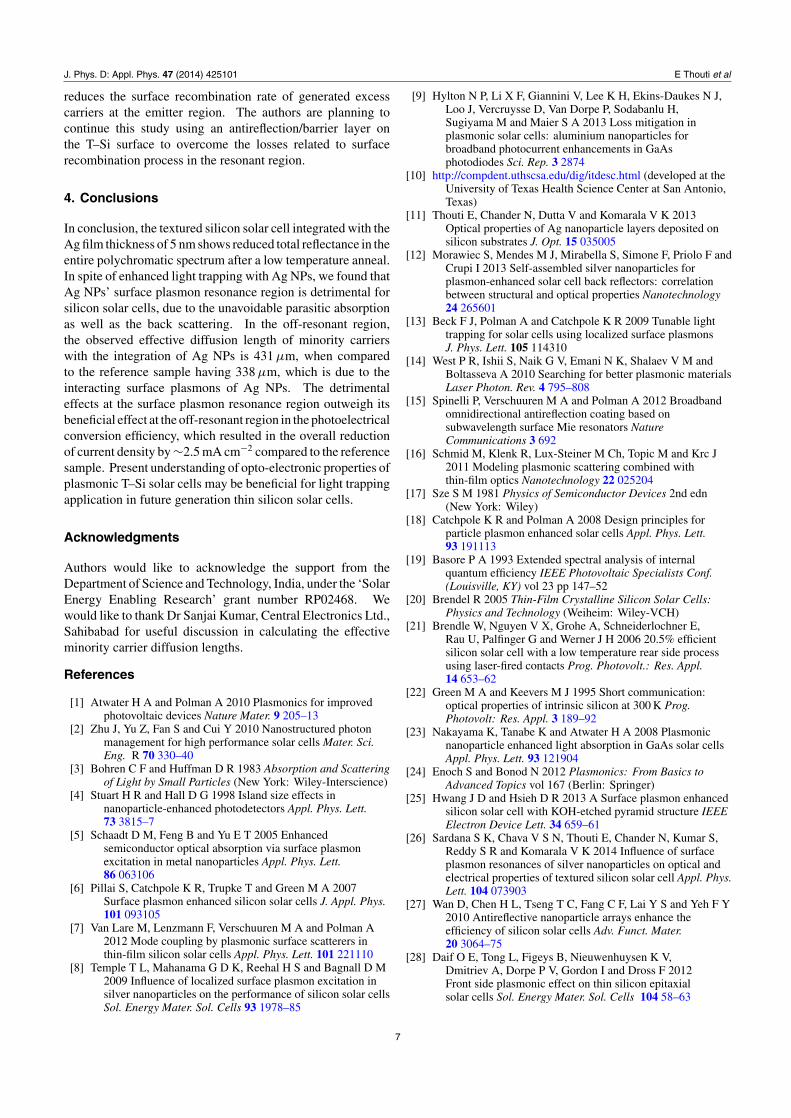
In order to obtain the Leff values of all the samples,IQE−1 versus cosθ /α graphs have been plotted using the datapoints in the 850 to 1020 nm wavelength region. Fitting theexperimental data results in straight lines and their inverseslope is taken as Leff . Figure 4 depicts the IQE−1 versus cosθ /αplots for samples C5, C10 and C15 annealed at temperatures300 and 400 ◦C, along with the sample C0. The calculated Leff
values from the plots are presented in table 1. The large changein the diffusion lengths with Ag NPs have been observed for thesamples C5 and C10. The observed maximum value of Leff forthe sample C5 is 431 µm with annealing temperature 300 ◦C,which is reduced to 392 µm after increasing the annealingtemperature to 400 ◦C, while the reference sample C0 has a Leff
of 338 µm. For sample C10, the enhanced Leff values are ∼391µm, which are nearly independent of annealing temperatures.But, for samples C3 and C15, Leff values are not affected much.
Effective diffusion lengths of minority carriers in the baseregion are associated with the lifetimes, the back surfacerecombination process (which are injection dependent) [20],and also collection probability. Calculated Leff of sample C0(338 µm) is longer than the cell thickness (200 ± 10 µm), so,the collection probability of generated carriers is expected to be
5
J. Phys. D: Appl. Phys. 47 (2014) 425101 E Thouti et al
Figure 4. Inverse of IQE versus Cosθ /α plots of textured siliconsolar cells without (C0) and with Ag NPs prepared from (a) 5 nm(C5), (b) 10 nm (C10) and (c) 15 nm (C15) Ag film annealed at 300and 400 ◦C. Solid points represent the experimental data and straightlines represent the fitted curves.
efficient. The enhancement of the Leff with the plasmonic T–Sicell may be due to the angular scattered light far-fields fromNPs, which can generate additional electron–hole pairs (closeto the p–n junction) in the base region leading to the mean pathlength enhancement of charge carriers. Usually the Shockley–Read–Hall (SRH) recombination process dominates in the baseregion of the cell and the saturated defects/traps related toSRH sites cannot influence the excess carriers generated bythe scattered field of NPs significantly. This can also easilyenhance the effective diffusion lengths of the carriers generatedfar from the p–n junction. The measurement of minority carrierlifetimes can give an idea about the modified recombination
Table 1. Calculated effective minority carrier diffusion lengths oftextured silicon solar cells without and with Ag NPs prepared fromAg film thicknesses of ∼3, 5, 10 and 15 nm and annealed at 300 and400 ◦C.
Effective diffusion length (µm)
338
Ag∼ 3 nm Ag∼ 5 nm Ag∼ 10 nm Ag∼ 15 nmCO (C3) (C5) (C10) (C15)
300◦ 340 431 391 334400◦ 344 392 394 347
process in the plasmonic T–Si cell with the excitation ofresonant and off-resonant wavelengths.
From the sample C5 (optimized Ag NPs size and density),we can infer that the Ag NPs are injecting some more lightinto the active silicon layer in addition to the incident light forincreasing the power generating electrons in the off-resonantregion. Usually, the absorption/scattering cross sections ofmetal NPs exceed the geometric cross sections at the resonantcondition. When the NPs are dense enough then there is apossibility of surface plasmon resonant interaction amongstthem; these interacting surface plasmons can enhance thelight transmission into the silicon [11, 23]. The incident lightfields stimulate a self-consistent interaction between adjacentNPs through charge cluster oscillations. When the NPsare interacting, establishing or overlapping plasma fields canprovide and sustain long wavelength hybrid modes [24]. Someof the modes could be guided through the silicon material andalso along the silicon surface, which would enhance the lighttransmission into silicon. Silver NPs separated by a certaindistance result in weakly interacting surface plasmons and thusthe corresponding light transmission into the cell is lowered,but the Leff values are still higher for some samples (like C10).Despite the enhanced Leff values in the off-resonant region,the overall photocurrent is reduced with Ag NPs due to thesignificant losses in the surface plasmon resonant region.
Textured silicon surface morphology can also stronglyinfluence the angular distribution of the scattered fields of NPsapart from the NPs sizes and concentration [25, 26], where thesimultaneous interaction of light at nanoscale metal particlesand micrometre scale textured surface may be complicated.The textured silicon surface having sharp and small sizedpyramidal structures are good for plasmonic light trapping,and also for improving the plasmonic device performance[25, 26], when compared to the wide and large sized pyramidalstructures where the back scattering is dominant, as observedin the present study. In our experimental observations,the reduced current densities are minimal (2.5 mA cm−2, forsample C5) even with the large surface coverage of AgNPs (figure 1(a)), when compared to the large reduction incurrent density of 19 mA cm−2 with a surface coverage ofonly ∼1.9% reported by other group [27]. Silver nanodiscsprepared by a hole–mask colloidal lithography technique onthin silicon solar cells have also shown similar magnitude(∼2 mA cm−2) of reduced current density [28]. Our simplenon-wetting evaporation technique may have some advantagesover colloidal lithography. Usually the anti-reflection layer
6
J. Phys. D: Appl. Phys. 47 (2014) 425101 E Thouti et al
reduces the surface recombination rate of generated excesscarriers at the emitter region. The authors are planning tocontinue this study using an antireflection/barrier layer onthe T–Si surface to overcome the losses related to surfacerecombination process in the resonant region.
4. Conclusions
In conclusion, the textured silicon solar cell integrated with theAg film thickness of 5 nm shows reduced total reflectance in theentire polychromatic spectrum after a low temperature anneal.In spite of enhanced light trapping with Ag NPs, we found thatAg NPs’ surface plasmon resonance region is detrimental forsilicon solar cells, due to the unavoidable parasitic absorptionas well as the back scattering. In the off-resonant region,the observed effective diffusion length of minority carrierswith the integration of Ag NPs is 431 µm, when comparedto the reference sample having 338 µm, which is due to theinteracting surface plasmons of Ag NPs. The detrimentaleffects at the surface plasmon resonance region outweigh itsbeneficial effect at the off-resonant region in the photoelectricalconversion efficiency, which resulted in the overall reductionof current density by ∼2.5 mA cm−2 compared to the referencesample. Present understanding of opto-electronic properties ofplasmonic T–Si solar cells may be beneficial for light trappingapplication in future generation thin silicon solar cells.
Acknowledgments
Authors would like to acknowledge the support from theDepartment of Science and Technology, India, under the ‘SolarEnergy Enabling Research’ grant number RP02468. Wewould like to thank Dr Sanjai Kumar, Central Electronics Ltd.,Sahibabad for useful discussion in calculating the effectiveminority carrier diffusion lengths.
References
[1] Atwater H A and Polman A 2010 Plasmonics for improvedphotovoltaic devices Nature Mater. 9 205–13
[2] Zhu J, Yu Z, Fan S and Cui Y 2010 Nanostructured photonmanagement for high performance solar cells Mater. Sci.Eng. R 70 330–40
[3] Bohren C F and Huffman D R 1983 Absorption and Scatteringof Light by Small Particles (New York: Wiley-Interscience)
[4] Stuart H R and Hall D G 1998 Island size effects innanoparticle-enhanced photodetectors Appl. Phys. Lett.73 3815–7
[5] Schaadt D M, Feng B and Yu E T 2005 Enhancedsemiconductor optical absorption via surface plasmonexcitation in metal nanoparticles Appl. Phys. Lett.86 063106
[6] Pillai S, Catchpole K R, Trupke T and Green M A 2007Surface plasmon enhanced silicon solar cells J. Appl. Phys.101 093105
[7] Van Lare M, Lenzmann F, Verschuuren M A and Polman A2012 Mode coupling by plasmonic surface scatterers inthin-film silicon solar cells Appl. Phys. Lett. 101 221110
[8] Temple T L, Mahanama G D K, Reehal H S and Bagnall D M2009 Influence of localized surface plasmon excitation insilver nanoparticles on the performance of silicon solar cellsSol. Energy Mater. Sol. Cells 93 1978–85
[9] Hylton N P, Li X F, Giannini V, Lee K H, Ekins-Daukes N J,Loo J, Vercruysse D, Van Dorpe P, Sodabanlu H,Sugiyama M and Maier S A 2013 Loss mitigation inplasmonic solar cells: aluminium nanoparticles forbroadband photocurrent enhancements in GaAsphotodiodes Sci. Rep. 3 2874
[10] http://compdent.uthscsa.edu/dig/itdesc.html (developed at theUniversity of Texas Health Science Center at San Antonio,Texas)
[11] Thouti E, Chander N, Dutta V and Komarala V K 2013Optical properties of Ag nanoparticle layers deposited onsilicon substrates J. Opt. 15 035005
[12] Morawiec S, Mendes M J, Mirabella S, Simone F, Priolo F andCrupi I 2013 Self-assembled silver nanoparticles forplasmon-enhanced solar cell back reflectors: correlationbetween structural and optical properties Nanotechnology24 265601
[13] Beck F J, Polman A and Catchpole K R 2009 Tunable lighttrapping for solar cells using localized surface plasmonsJ. Phys. Lett. 105 114310
[14] West P R, Ishii S, Naik G V, Emani N K, Shalaev V M andBoltasseva A 2010 Searching for better plasmonic materialsLaser Photon. Rev. 4 795–808
[15] Spinelli P, Verschuuren M A and Polman A 2012 Broadbandomnidirectional antireflection coating based onsubwavelength surface Mie resonators NatureCommunications 3 692
[16] Schmid M, Klenk R, Lux-Steiner M Ch, Topic M and Krc J2011 Modeling plasmonic scattering combined withthin-film optics Nanotechnology 22 025204
[17] Sze S M 1981 Physics of Semiconductor Devices 2nd edn(New York: Wiley)
[18] Catchpole K R and Polman A 2008 Design principles forparticle plasmon enhanced solar cells Appl. Phys. Lett.93 191113
[19] Basore P A 1993 Extended spectral analysis of internalquantum efficiency IEEE Photovoltaic Specialists Conf.(Louisville, KY) vol 23 pp 147–52
[20] Brendel R 2005 Thin-Film Crystalline Silicon Solar Cells:Physics and Technology (Weiheim: Wiley-VCH)
[21] Brendle W, Nguyen V X, Grohe A, Schneiderlochner E,Rau U, Palfinger G and Werner J H 2006 20.5% efficientsilicon solar cell with a low temperature rear side processusing laser-fired contacts Prog. Photovolt.: Res. Appl.14 653–62
[22] Green M A and Keevers M J 1995 Short communication:optical properties of intrinsic silicon at 300 K Prog.Photovolt: Res. Appl. 3 189–92
[23] Nakayama K, Tanabe K and Atwater H A 2008 Plasmonicnanoparticle enhanced light absorption in GaAs solar cellsAppl. Phys. Lett. 93 121904
[24] Enoch S and Bonod N 2012 Plasmonics: From Basics toAdvanced Topics vol 167 (Berlin: Springer)
[25] Hwang J D and Hsieh D R 2013 A Surface plasmon enhancedsilicon solar cell with KOH-etched pyramid structure IEEEElectron Device Lett. 34 659–61
[26] Sardana S K, Chava V S N, Thouti E, Chander N, Kumar S,Reddy S R and Komarala V K 2014 Influence of surfaceplasmon resonances of silver nanoparticles on optical andelectrical properties of textured silicon solar cell Appl. Phys.Lett. 104 073903
[27] Wan D, Chen H L, Tseng T C, Fang C F, Lai Y S and Yeh F Y2010 Antireflective nanoparticle arrays enhance theefficiency of silicon solar cells Adv. Funct. Mater.20 3064–75
[28] Daif O E, Tong L, Figeys B, Nieuwenhuysen K V,Dmitriev A, Dorpe P V, Gordon I and Dross F 2012Front side plasmonic effect on thin silicon epitaxialsolar cells Sol. Energy Mater. Sol. Cells 104 58–63
7