Embed Size (px)
Citation preview

Interface Products Business LineSystem Management Product Line
Designing with I2C Fm+
January 2014Peter Stonard – Applications Engineer

2
Welcome!
This Webinar focuses on the recently released NXP OM13320 Fm+ Development Kit.
Detailed instruction will be given to power up the kit, connect it to a computer running Win7, and exercise the supplied NXP GUI support software.
To drive the kit you will need a Computer (running Win7/64)

What we will cover today
Just what is an I2C Bus?
Why the NXP Fm+ Development Board was created
What you can (and can’t) do with it
First time set up (Jumpers and USB Driver)
How to set up a “trade show demo”
How to install firmware on the MCU
How to set up and use the NXP GUI
3

4
I2C Introduction
4

Do you know about I2C Basics?
This is a popular low speed digital serial bus system
(under one megabits/second)
The I2C Bus is used in many applications, from small scale to large
Many semiconductor vendors use the I2C Bus, or one of its derivatives (SMBus being the most widely known)
5

Why I2C?
Devices that can talk to each other, on the I2C bus, have been available for a long time, and new ones are being added regularly
There are two features that make the I2C Bus unique and popular1 – Combination of both Hardware and protocol (open standard)2 – Hardware is very simple (two wires, two resistors!)
6
M SSCL
SDA
GND
VDD
GND
VDD
Pull Up Resistors on each line

I2C Applications
Sensors and Displays
Expanding Input/Output (digital IO)
Data storage and transfer
7

End products with I2C inside
Industrial Controls
Personal Electronics
White Goods/Home Appliances
8

What is the Protocol Layer?
Protocol Layer = Data format, traffic, collision arbitration
An I2C Bus must have:Two node types (Master and Slave)Minimum of ONE Slave and ONE Bus Master
9
M SI2C Bus
SLAVEBUS CONTROLLER

What is the Physical Layer?
Physical Layer = electrical connections
Two Wires: Data and Clock (plus ground and supply)
Data line (SDA)
Clock line (SCL)
10
VDD
M SSCL
SDA
GND
VDD
GND
VDD
Pull Up Resistors on each line

How Fast can I2C Operate?
Messages on the I2C Bus Data line (SDA) are synchronized
By a clock signal on the Clock line (SCL)
Clock is generated by the Bus Master, not by the Slave
Originally the fastest clock was 100kHz, now called Standard-Mode
Over time this was raised. First to 400kHz, called Fast-Mode (Fm)
Then to 1MHz (1000kHz) called Fast-Mode Plus (Fm+)
There is no lower limit, the bus can ‘rest’ or ‘stall’ at DC
The Fm+ Development kit only has Fm+ rated I2C parts
Any other parts (Standard-Mode, or Fast-Mode) can be mixed together
11

What Voltage Operates I2C?
Because I2C was invented in the days of “five volt logic” it is 5V
However, 5V is rare in new designs, making today’s I2C “any voltage”
The I2C Bus is made backwards compatible using appropriate I2C devices, or clever circuit tricks
NXP has new I2C devices that require as low as 0.8V for power
Most of today’s I2C designs are for 3.3V, and sometimes 2.5V
Near future applications are probably between 1V and 1.8V
12

Why do we need a Development Board?
The NXP I2C products are part of a system – they can’t work alone
Some I2C parts are simple (Bus Buffers are not protocol aware)
Some I2C parts are complex (Many registers must be set up first)
The I2C devices on the board require an I2C Master (MCU & firmware)
The modular design allows add-ons to be created and used later
13

What to do with the Fm+ Development Kit
1. Trade show “eye candy” to get attention
2. Customer demos of specific I2C devices
3. Engineering evaluation of I2C devices
Some Engineering examples:
o Learn how a specific I2C device operates
o Compare I2C devices across brands and types
o Project PoC (Proof of Concept) before building hardware
o Operate a device in a specific set up
o Measure performance (using external tools)
14

15
What’s in the box?
15

What’s in the Box?
16

The Main Board
The kit is built around an I2C
specific PCB (OM13260)
Most of the time it is connected to PC (via USB) for Power and Control
It can be used without the PC (DC power adapter)
The board has a variety of I2C devices, and two separate I2C Buses
17

Add-On to the Kit
New I2C Products (not released at this time)
I2C device hardware design (build your circuit on the PCB)
Benchmark (made measurements and side-by-side comparisons)
18

19
Take A Quick Tour
19

I2C Bus Masters
20

I2C Bus Slaves
21

22
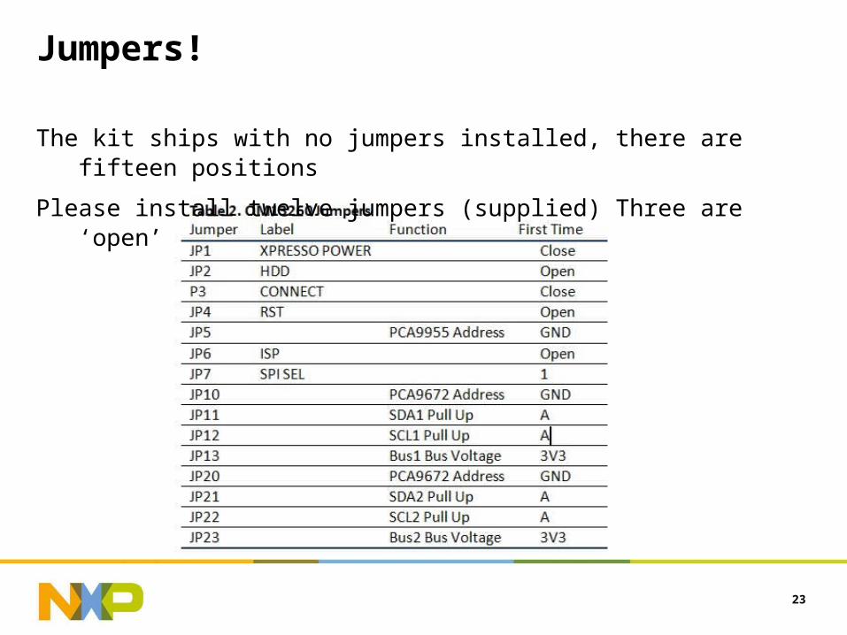
Jumpers!
The kit ships with no jumpers installed, there are fifteen positions
Please install twelve jumpers (supplied) Three are ‘open’
23

Fm+ Development Board Floor Plan
24
Bus 1
Bus 2
USB &Power
Bus Pull Ups
GPIOLED
Driver
Proto Area
Utilities
PORT D PORT C
PORT A PORT B
PORT E
TESTER
TESTER
USB
DC POWER
GPIO OUTPUTS
GPIO OUTPUTS

25
How to install USB Driver
25

USB Driver Installation
Summary
Win7/64 will attempt to auto-install a driver when the Fm+ Development Board is attached by USB for the first time
However, this is not the required driver to operate with the NXP GUI
Overview
Using the Device Manager, remove the default USB driver
Select the driver supplied in the NXP GUI distribution
Install the correct driver using the Windows installer
26

Connect the FM+ Hardware for the first time
How to navigate to the Device Manager on your PC
1. Click the Windows ‘start’ button
2. Right Click the Computer
3. Select Properties
4. Select Device Manager
Device Manager
27

Remove the Default Driver
28
1. Open “Other devices”
2. Right click on NXP FM+ DEV BOARD

Update Driver Software
Select the first option Update Driver Software..
29

Select the new driver location
Select the second option “Browse my computer for driver software”
30

Select the USB Driver from the Distribution
31
C:\Program Files (x86)\NXP FM+ Development Board Software\
drivers

Bypass the Warning
Select “Install this driver software anyway”
32
Installation may take several minutes

Verify the new driver is installed
33
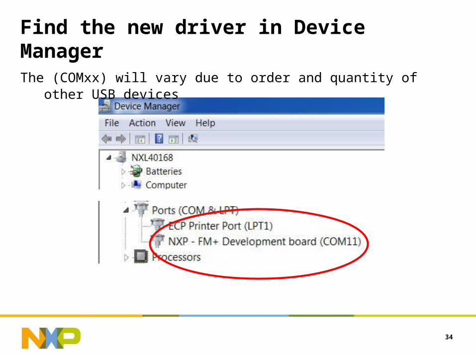
Find the new driver in Device Manager
The (COMxx) will vary due to order and quantity of other USB devices
34

35
“Trade Show Demo”
35

What is a “Trade Show Demo”?
Blinky lights get attention!
Custom firmware will run a lightshow
There is no need for a computer or other software
The Fm+ Development Board has a 16channel LED driver
Four RGB LED clusters, and four White LEDs
GPIO Target Boards (in the kit) add more LEDs (“cylon eyes”)
Use any USB port, USB power adapter or AC-DC power adapter
36

Install the “Port E” Jumper
The Fm+ Development Board has two I2C buses: Bus1 and Bus2
Use a two wire jumper to make one bus by joining them together
Install a two-wire Jumper (supplied) as shown
Important! Add a twist as shown
37

Attach the GPIO Target Board
From the kit identify two GPIO Target Boards (OM13303)
Also, two 10pin Ribbon Cables
The hardware kit ( borrow a #0 Phillips screwdriver)
38

1. Attach the ribbon cables to the bottom of the GPIO Target Board
Note: Red stripe on cable matches white mark on PCBs
2. Assemble the hardware as shown
3. Attach the GPIO target Boards to the Fm+ Development Board
Connect the GPIO Target Boards
39

40
How to install firmware
40

Firmware Installation
Summary
The processor on the board requires firmware
This is installed over the USB link, from a computer (Win7/64)
It is unlikely that the board will be ‘bricked’
Overview
The board is put into ISP (In System Program) mode
Any existing file(s) on the MCU are deleted
A firmware hex file is written into the MCU memory (32kB max)
The board is removed from ISP mode and reset
41

ISP Mode (Jumper and Reset)
Attached the USB Cable
Install a Jumper on JP6 “ISP”
Install a Jumper on JP4 “RST”
Remove the Jumper from JP4
42

Open the Windows Explorer on your computer
Find the newly added drive (E: in this example)
Open the folder
Delete the file “firmware.bin”
Delete existing firmware (in CRP DISABLED)
43

Install the new firmware (on the MCU)
Copy and Paste the desired firmware to CRP DISABLED
The two firmware files in the distribution are (pick one):1. Standalone_trade_show_FM+_DEMO.bin2. FM+DevelopmentBoard V03_00.bin
44

45
Running the Trade Show Demo
Remove Installed Jumper on JP6 “ISP”
Reset the Fm+ Development Board (briefly close JP4)
Each time the board is powered up the demo will start automatically
Use a 6V 2A AC-DC Adapter, USB ‘brick’, or any USB cable
Digikey PN 62-1132-ND (Not Supplied)

46
NXP GUI
46

What is a GUI?
The Graphical User Interface (GUI) is an API (Application Program Interface) that runs on an appliance under Windows7/64 OS
Once installed the GUI will communicate with the NXP hardware over a USB cable. The USB port powers the hardware.
47

What can and can’t the GUI do?
The NXP GUI supports the three I2C devices on the OM13260 board
Future devices will require updates to the GUI
Scripts can be written in the GUI to operate any I2C device attached to the OM13260 board (through daughter cards)
The NXP GUI requires installation of the correct firmware on the MCU
The GUI is written in National Instruments LabView, and distributed as a royalty-free executable (approx 150MB)
Currently there is no support for edits or revision to the NXP GUI
The NXP GUI only supports Win7/64 OS
48

49
Install the NXP GUI Firmware
Repeat the section “How to install GUI firmware”
Install the “FM+DevelopmentBoard V03_00.bin” firmware
Reset the OM13260 Board (briefly close JP4 RST)
Open the NXP GUI API on your computer

NXP GUI Welcome Screen
50

NXP GUI Device Selection Screen
51
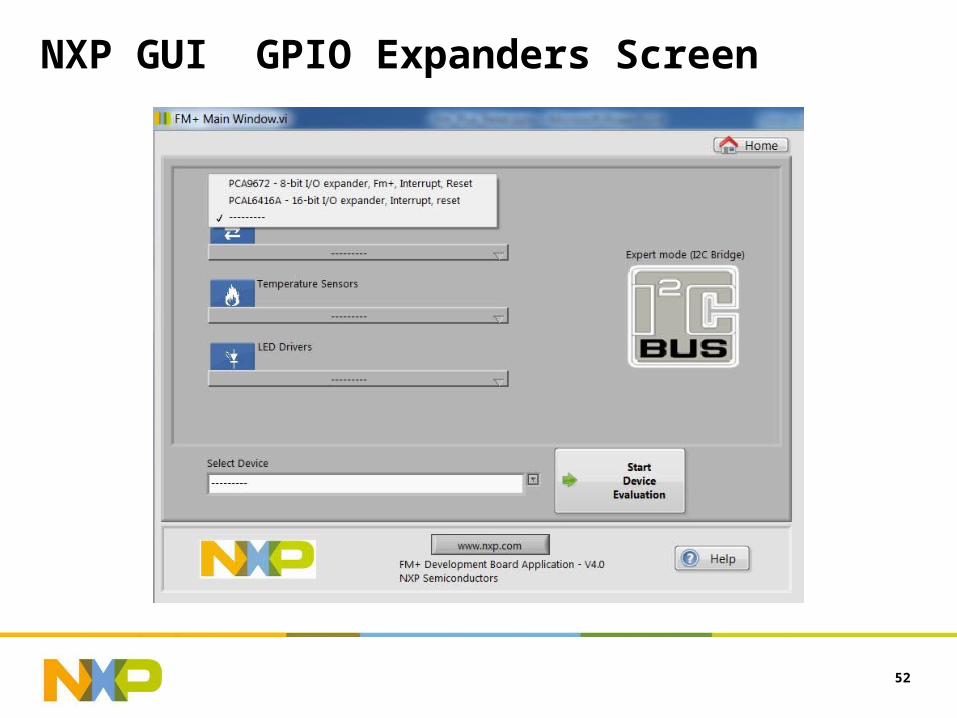
NXP GUI GPIO Expanders Screen
52

NXP GUI Temperature Sensors Screen
53

NXP GUI LED Drivers Screen
54

NXP GUI Select Device Screen
55

56
NXP GUI GPIO
56

What is a GPIO?
The General purpose Input Output devices are I2C Slaves
Instructions in I2C messages control several IO Ports
Ports can source or sink current to a load
Ports can also be read by the Bus Master
“PCA9672 Remote 8-bit I/O expander for Fm+ I2C-bus with interrupt and reset”
57

GPIO Hardware (PCA9672)
58
Each of the two buses on the OM13260 board has an 8-bit GPIO
Four address options each (JP10 for bus1 and JP20 for bus2)
HEX 8-bit NXP 7-bit
PCB MSB LSB GUI MSB LSB
GND 0x44 0100 0100 0x22 0010 0010VCC 0x46 0100 0110 0x23 0010 0011
SCL 0x54 0101 0100 0x2A 0010 1010
SDA 0x56 0101 0110 0x2B 0010 1011

Using the GPIO Target
59
Outputs can be monitored with the GPIO Target board (OM13303)
GPIO Target Board has eight channels, each with an LED and switch
The NXP GUI can drive the LEDs (GRN = 1, RED = 0)
The NXP GUI can read the switches (Press = 0)

NXP GUI Select Device Screen (GPIO)
60
61
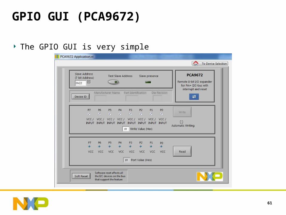
GPIO GUI (PCA9672)
The GPIO GUI is very simple

GUI Slave Address and Test
62
Start by setting the Address and then press Test Slave Address

Driving the LEDs
63
Write to the LEDs (VCC = open, GND = RED LED on)

Reading the switches
64
Read the switches (VCC = open, GND = pressed)

65
NXP GUI LED Driver
65

What is a LED Driver?
The LED Driver devices are I2C Slaves
Instructions in I2C messages control IO Chanels
Intended for driving LEDs, the channels sink constant current
Control of LED current, Pulse Width Modulation (PWM), Group PWM and Blinking, are made by the Bus Master
Health of the LEDs is monitored and reported to the Bus Master
There are 55 8-bit registers in the device, required to operate it
“PCA9955 16-channel Fm+ I2C-bus 57 mA constant current LED driver”
66

NXP GUI Select Device Screen (LED driver)
67

LED Driver Hardware (PCA9955)
68
Bus1 on the OM13260 board has a 16 channel LED Driver
Two address options (JP5)
HEX 8-bit NXP 7-bitPCB MSB LSB GUI MSB LSB
GND 0xC0 1100 0000 0x60 0110 0000
VCC 0xD0 1101 0000 0x68 0110 1000

LED Driver Hardware (PCA9955)
69
Outputs 0 – 11 drive four RGB LEDs clusters
Outputs 12 – 15 drive four White LEDs
LEDs current is set by the Driver (no extra resistors)
Adjust R36 to set max LED current
(leave it set to 50%)

LED GUI (PCA9955)
70
The PCA9955 has 55 internal registers, making the GUI complex

Getting Started with the PCA9955
71
1. Test the Slave Address, and note “Slave Presence” is now green
2. From the drop down menu select “LED0”
3. From the Output State select “ON”

Lighting LED0
72
1. Note the Red LED (LED0 an RGB cluster) is full on
2. Move the slider up and down in the “output gain control” (0 – 255)
3. Note that Red LED fades up and down
4. Reset the “output gain control” to 100

Driving with PWM
73
1. Change the Output State drop down menu to “PWM”
2. Note the large rotary dial is now live (not grayed-out)
3. Use this to change the LED0 brightness
4. Leave the PWM dial at 100
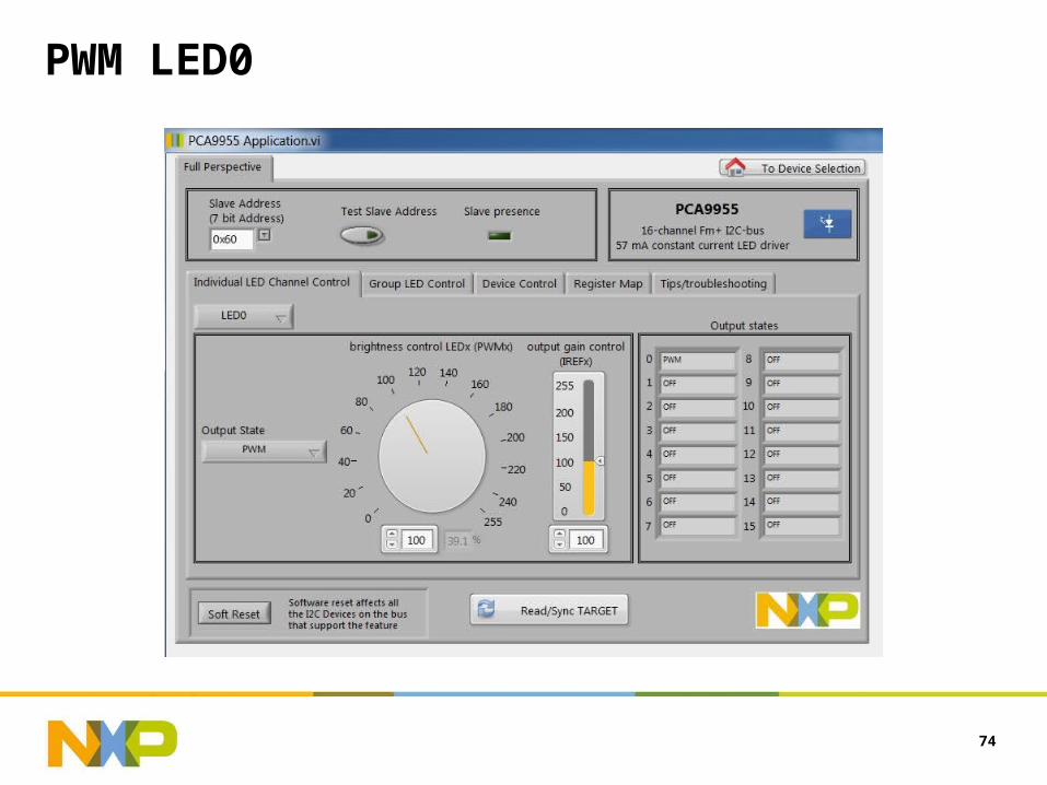
PWM LED0
74

1. Repeat the earlier steps to select several LEDs one at a time
2. Set each one to “PWM and GRPPWM”
3. Note “Output states” status
4. Set each LED output gain to 100
5. Set each LED PWM to 100
6. Try these:
LED0, LED4, LED8 and LED13
Group Control Selection
75

Group Control PWM
76
1. Move to the second Tab “Group LED Control”
2. Set IREFALL = 100
3. Set PWMALL = 100
4. Move the rotary dial
Note that all selected
LEDs dim together

Group Control Blinking
77
1. Select the Group = blinking button
2. Set “Blinking period” = 5 (cycle time is 0.393 seconds or about 3Hz)
3. Move the rotary dial
Note all selected LEDs
Blink together
The rotary dial sets the
Duty-cycle of the blink

Adjusting the Max LED Current (R36 Pot)
Using a Philips #0 screwdriver adjust R36
Note that turning the screwdriver CW increased the LED drive
The Fm+ Kit will be safe, even if LEDs are full on and R36 at max CW
The PCA9955 has thermal shutdown. It will ‘burp’ if driven too hard
To drive all the LEDs at max current will require an external 6V 2A AC/DC Adapter Digikey PN 62-1132-ND (Not Supplied)
Remember to return the Pot (R36) to 50% after this experiment!
78

79
NXP GUI Expert Mode
79
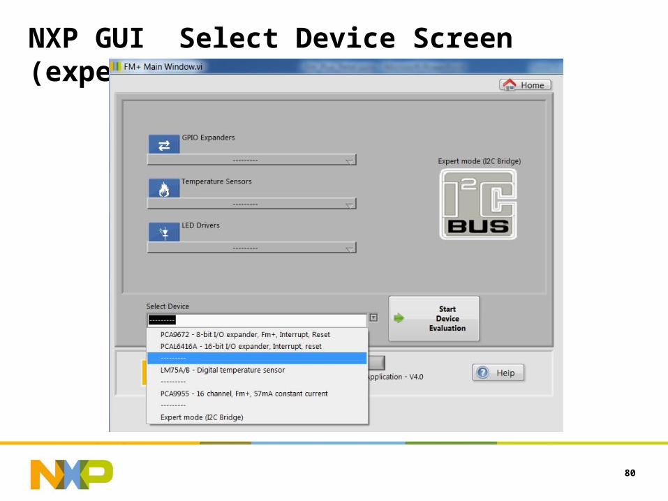
NXP GUI Select Device Screen (expert mode)
80

NXP GUI Expert Mode Screen
81

NXP GUI PCA9672 Sample Screen
82

NXP GUI PCA9672 Sample Running Screen
83

NXP GUI Expert Mode (File Management)
84
The NXP GUI distribution includes one expert mode example
This is installed here:
C:\Program Files (x86)\NXP FM+ Development Board Software\User Scripts
This file location may be write protected on your OS
Find a new place to store the files that you create or edit

NXP GUI Expert Mode (File Editing)
85


![Programming Guide I2C Bus - chip1stop.com · 14.07.2016 · [1][2] It is need adjust resister value when i2c bus line don't have stable. [3][4] It is value up to speed of mcu's i2c](https://img.pdfslide.us/doc/110x75/5f6ba957d0a76a472813f38e/programming-guide-i2c-bus-14072016-12-it-is-need-adjust-resister-value.jpg)