Embed Size (px)
Citation preview
1Professor N Cheung, U.C. Berkeley
Lecture 17EE143 S06
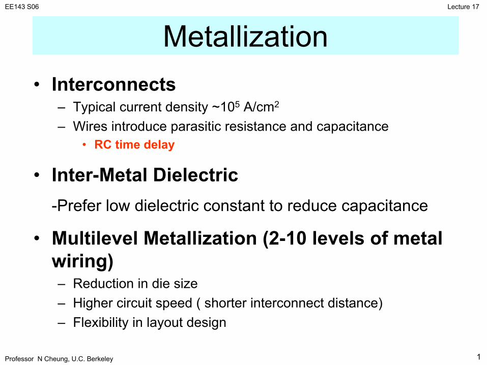
Metallization• Interconnects
– Typical current density ~105 A/cm2
– Wires introduce parasitic resistance and capacitance• RC time delay
• Inter-Metal Dielectric-Prefer low dielectric constant to reduce capacitance
• Multilevel Metallization (2-10 levels of metal wiring)– Reduction in die size– Higher circuit speed ( shorter interconnect distance)– Flexibility in layout design

2Professor N Cheung, U.C. Berkeley
Lecture 17EE143 S06
FOX
Si substrate
( InteMetal Oxide e.g. BPSG. Low-K dieletric)
(e.g. PECVD Si Nitride)

3Professor N Cheung, U.C. Berkeley
Lecture 17EE143 S06
• Interconnections and Contacts– RC Time Delay– Interconnect resistance– Contact resistance– Dielectric Capacitance– Reliability - Electromigration
• Multilevel Metallization • Surface Planarization Techniques
Outline
4Professor N Cheung, U.C. Berkeley
Lecture 17EE143 S06

5Professor N Cheung, U.C. Berkeley
Lecture 17EE143 S06
Interconnect ResistanceRI =R/L = ρ / (WAlTAl)
Interconnect-Substrate CapacitanceCV ≡C/L = WAl εox / Tox
Interconnect-Interconnect CapacitanceCL ≡ C/L = TAl εox / SAl
* Values per unit length L
Interconnect RC Time Delay
6Professor N Cheung, U.C. Berkeley
Lecture 17EE143 S06
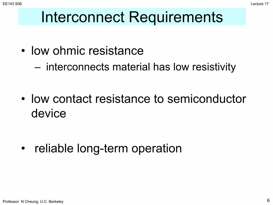
Interconnections Interconnect Requirements
• low ohmic resistance– interconnects material has low resistivity
• low contact resistance to semiconductor device
• reliable long-term operation

7Professor N Cheung, U.C. Berkeley
Lecture 17EE143 S06
• Metal (Low resistivity)
– for long interconnects
• Highly doped Poly-Si (medium resistivity)
–for short interconnects
• Highly doped diffused regions in Si substrate (medium resistivity)
–for short interconnects
Possible interconnect materials
8Professor N Cheung, U.C. Berkeley
Lecture 17EE143 S06
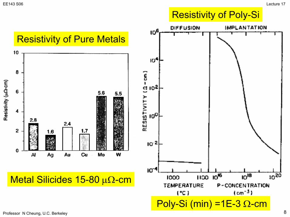
Resistivity of Poly-Si
Resistivity of Pure Metals
Metal Silicides 15-80 µΩ-cm
Poly-Si (min) =1E-3 Ω-cm

9Professor N Cheung, U.C. Berkeley
Lecture 17EE143 S06
Metal Contact to SiTunneling “ohmic” contacts
SiO2
Al
n+
n-Sie 1019 - 1021/cm3
SiO2
Al
p+
p-Si
Xd
Ec
Ev
I
Vh
MSi
> 1019/cm3

10Professor N Cheung, U.C. Berkeley
Lecture 17EE143 S06
Schottky RectifyingContact
SchottkyTunneling Ohmic Contact
Tunneling
Thermionic emission
Small depletion width(highly doped Si)
Large depletion width(lightly doped Si)
metal semiconductor
Depletion region
11Professor N Cheung, U.C. Berkeley
Lecture 17EE143 S06
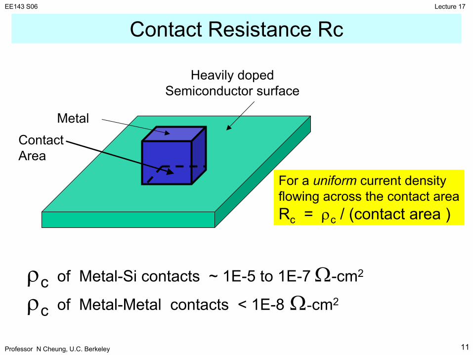
For a uniform current density flowing across the contact areaRc = ρc / (contact area )
ρc of Metal-Si contacts ~ 1E-5 to 1E-7 Ω-cm2
ρc of Metal-Metal contacts < 1E-8 Ω-cm2
MetalContact Area
Heavily dopedSemiconductor surface
Contact Resistance Rc
12Professor N Cheung, U.C. Berkeley
Lecture 17EE143 S06
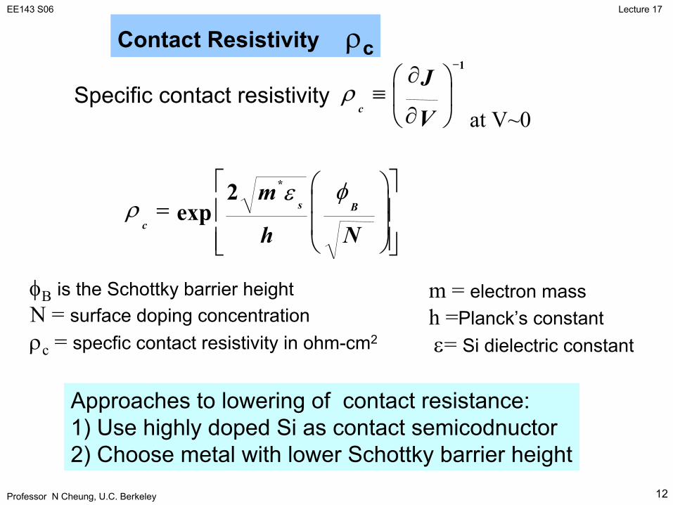
= Bs
c Nh
m φερ
*2exp
Approaches to lowering of contact resistance:1) Use highly doped Si as contact semicodnuctor2) Choose metal with lower Schottky barrier height
φB is the Schottky barrier heightN = surface doping concentrationρc = specfic contact resistivity in ohm-cm2
∂
∂≡
−
c V
Jρ
1
at V~0
m = electron massh =Planck’s constantε= Si dielectric constant
Specific contact resistivity
Contact Resistivity ρc

13Professor N Cheung, U.C. Berkeley
Lecture 17EE143 S06
Schottky Barrier heightsof common metals contactsto n-type semiconductors
Note:ΦB (n-type) + ΦB (p-type) = Eg of semiconductor

14Professor N Cheung, U.C. Berkeley
Lecture 17EE143 S06
Al Spiking Problem

15Professor N Cheung, U.C. Berkeley
Lecture 17EE143 S06
Al-Si Eutectic Behavior
At the sintering temperature of about 450C after metalization, Si is soluble in Al up to ~1 % but Al is not soluble in Si.

16Professor N Cheung, U.C. Berkeley
Lecture 17EE143 S06
1. Add ~2% Si to Al to prevent Si outdiffusion
2. Use diffusion barrier layer to block Al/substrate interaction
Al Spiking Problem: Solutions

17Professor N Cheung, U.C. Berkeley
Lecture 17EE143 S06
electron flow
moment transferredfrom electrons
Thermally excitedmetal atom out of lattice site
Metal Lattice atomic potential
position x
Electromigration Motion
Metal atom at lattice site(equilibrium)
•Electromigrated metal atoms move along the same direction of electrons
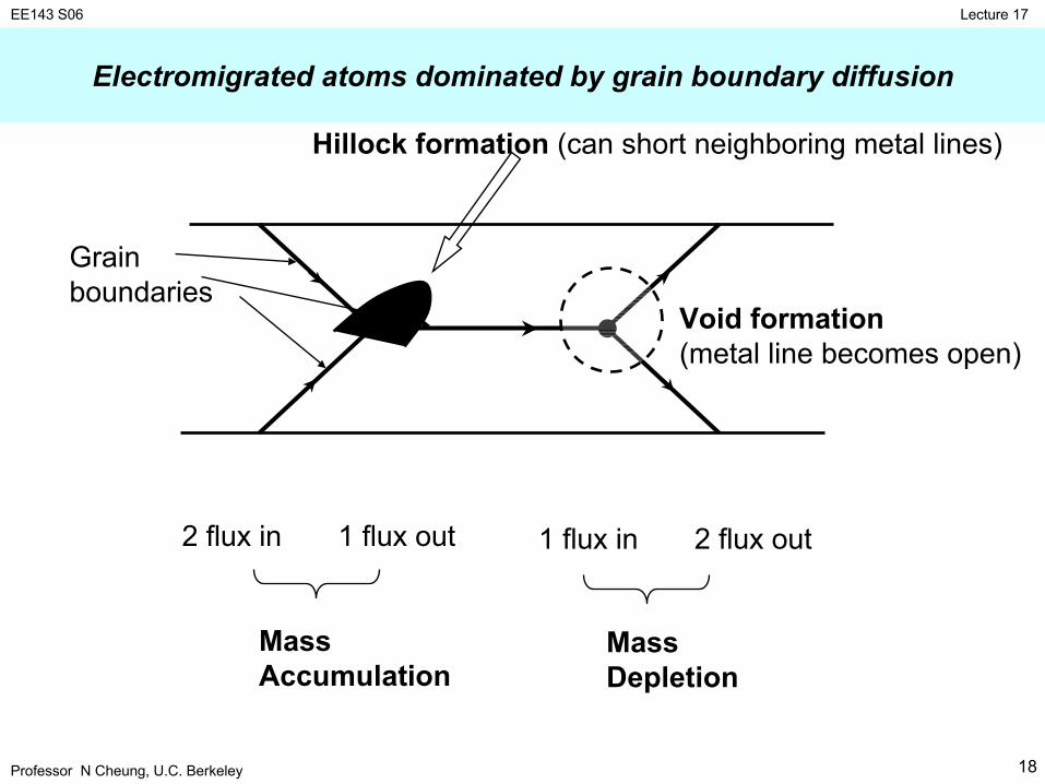
18Professor N Cheung, U.C. Berkeley
Lecture 17EE143 S06
Hillock formation (can short neighboring metal lines)
Void formation(metal line becomes open)
2 flux in 1 flux out
MassAccumulation
1 flux in 2 flux out
MassDepletion
Grainboundaries
Electromigrated atoms dominated by grain boundary diffusion

19Professor N Cheung, U.C. Berkeley
Lecture 17EE143 S06
Electron flow
HillockFormation
VoidFormation
LargeHillock (dendrite)
SEM micrographs ofAluminumelectromigrationfailure

20Professor N Cheung, U.C. Berkeley
Lecture 17EE143 S06
Dendrite Fomation Void Formation

21Professor N Cheung, U.C. Berkeley
Lecture 17EE143 S06
* MTF defined as time for 50% of test samples to fail
MTF ∝ J –2 exp [ EA/ kT]
J = current density in Amp/cm2EA = activation energy ( ~ 0.5-0.8 eV for metals)
Median Time to Failure (MTF) of Electromigration
22Professor N Cheung, U.C. Berkeley
Lecture 17EE143 S06
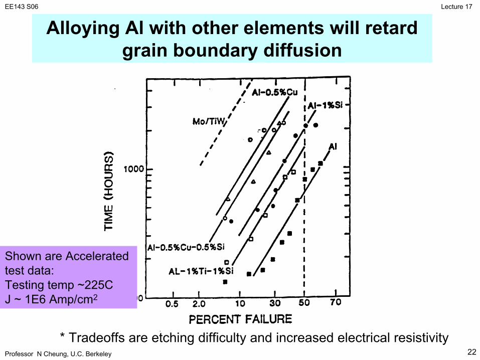
* Tradeoffs are etching difficulty and increased electrical resistivity
Shown are Accelerated test data:Testing temp ~225CJ ~ 1E6 Amp/cm2
Alloying Al with other elements will retard grain boundary diffusion

23Professor N Cheung, U.C. Berkeley
Lecture 17EE143 S06
How alloy precipitates can block grain boundary diffusion
Example: Al-Cu (1-4%) alloy. After sintering, AlCu3 compound willprecipitate along the grain boundaries.

24Professor N Cheung, U.C. Berkeley
Lecture 17EE143 S06
Suggested Metallization for 0.25µm linewidths
25Professor N Cheung, U.C. Berkeley
Lecture 17EE143 S06
Metal Deposition Techniques
• Sputtering has been the technique of choice – high deposition rate– capability to deposit complex alloy compositions– capability to deposit refractory metals– uniform deposition on large wafers– capability to clean contact before depositing metal
• CVD processes have recently been developed(e.g. for W, TiN, Cu)– better step coverage– selective deposition is possible– plasma enhanced deposition is possible for lower deposition
temperature
26Professor N Cheung, U.C. Berkeley
Lecture 17EE143 S06
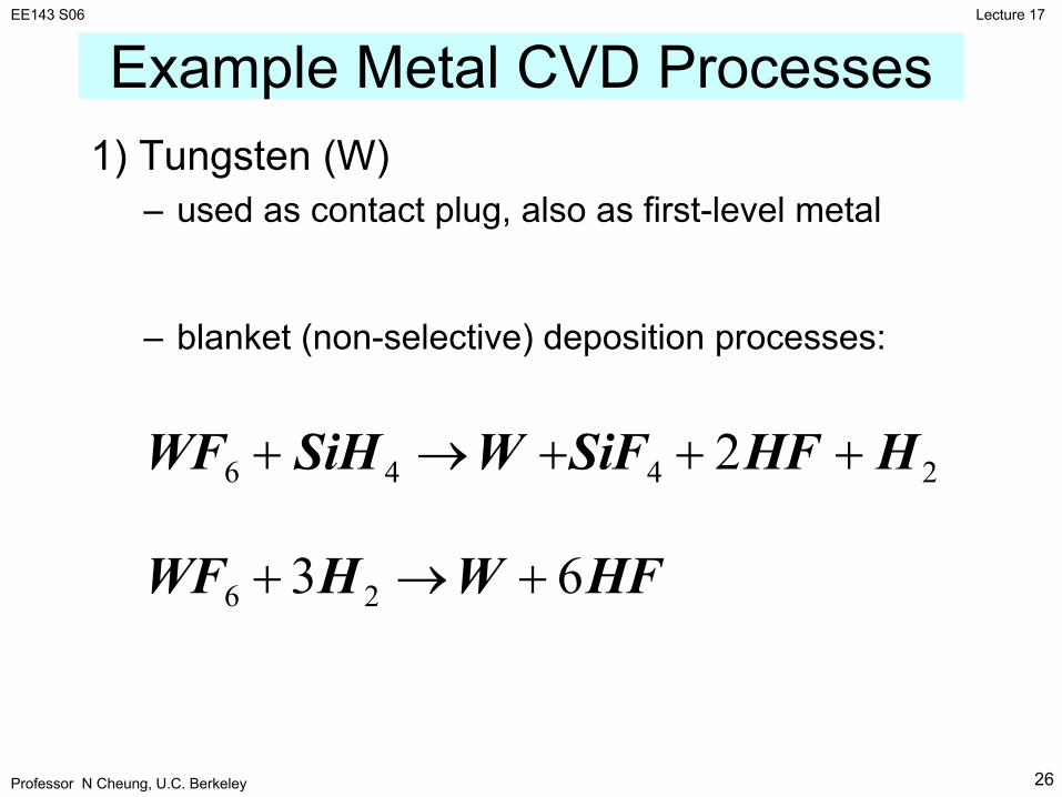
1) Tungsten (W)– used as contact plug, also as first-level metal
– blanket (non-selective) deposition processes:
HFWHWF 63 26 +→+
2446 2 HHFSiFWSiHWF +++→+
Example Metal CVD Processes

27Professor N Cheung, U.C. Berkeley
Lecture 17EE143 S06
2) TiN– used as barrier-metal layer
– deposition processes:
HClTiNHNHTiCl 8222 234 +→++
234 NHCl24TiN6NH8TiCl6 ++→+
HClTiNHNTiCl 8242 224 +→++
Metal CVD Processes (cont.)

28Professor N Cheung, U.C. Berkeley
Lecture 17EE143 S06
3) CVD Copper
Metal-OrganicCu compound (gas)

29Professor N Cheung, U.C. Berkeley
Lecture 17EE143 S06
Trench filling with CVD Cu
30Professor N Cheung, U.C. Berkeley
Lecture 17EE143 S06
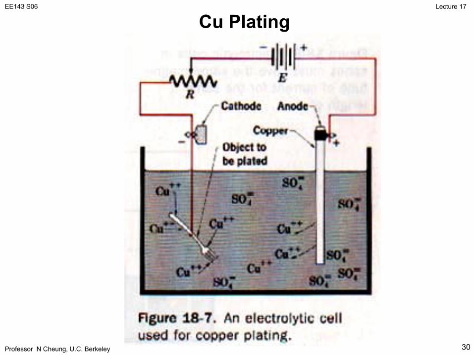
Cu Plating

31Professor N Cheung, U.C. Berkeley
Lecture 17EE143 S06
Electroless Cu Plating

32Professor N Cheung, U.C. Berkeley
Lecture 17EE143 S06
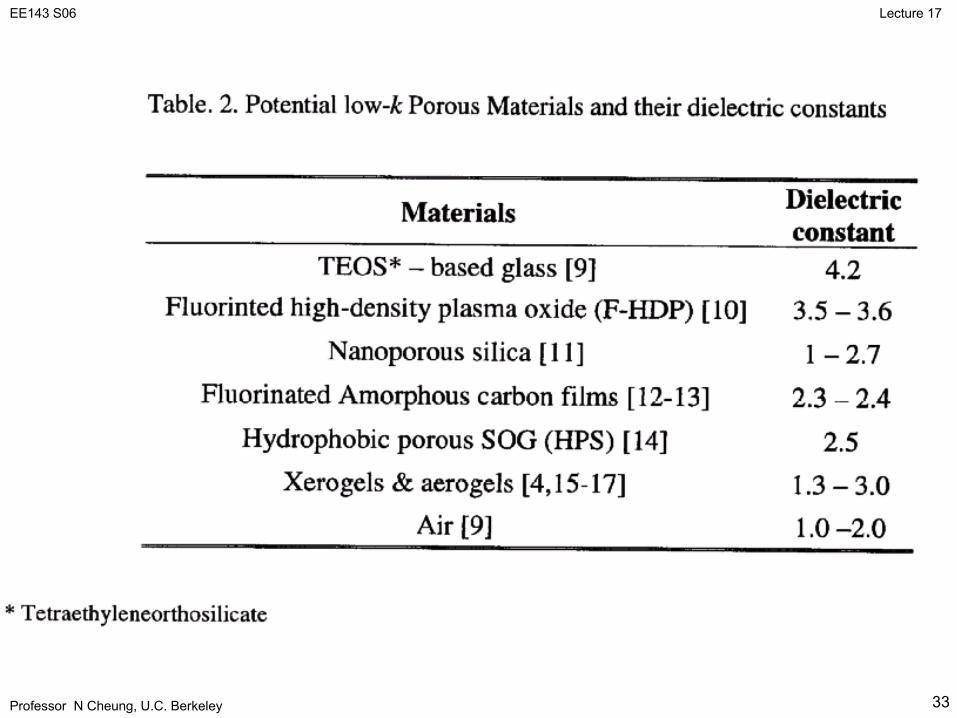
Low-K Dielectrics
33Professor N Cheung, U.C. Berkeley
Lecture 17EE143 S06

34Professor N Cheung, U.C. Berkeley
Lecture 17EE143 S06

35Professor N Cheung, U.C. Berkeley
Lecture 17EE143 S06
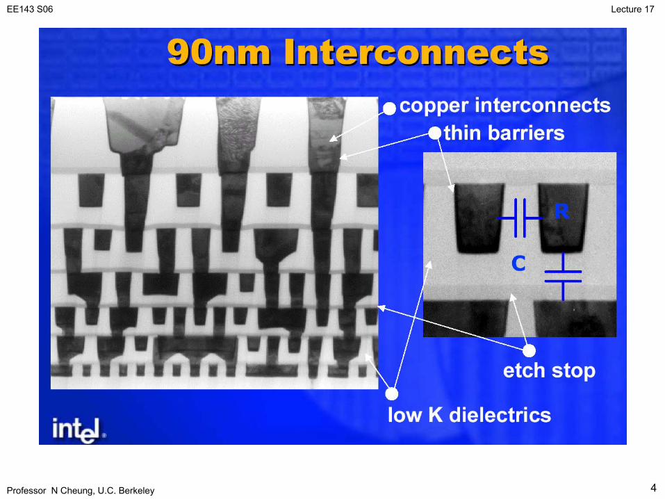
• Copper interconnects
• Low-K dielectrics(Fluorinated SiO2, polymers, xerogels...)
To further reduce RCtime delay:
Advanced Metalization Materials
*This photo is an idealizationonly, with an airgap betweenthe Cu layers.