Embed Size (px)
Citation preview
Professor N Cheung, U.C. Berkeley
Lecture 17EE143 F2010
NonplanarMetallization
PlanarMetallization
Professor N Cheung, U.C. Berkeley
Lecture 17EE143 F2010
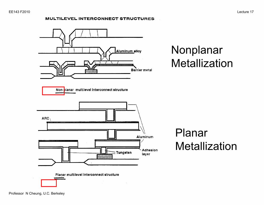
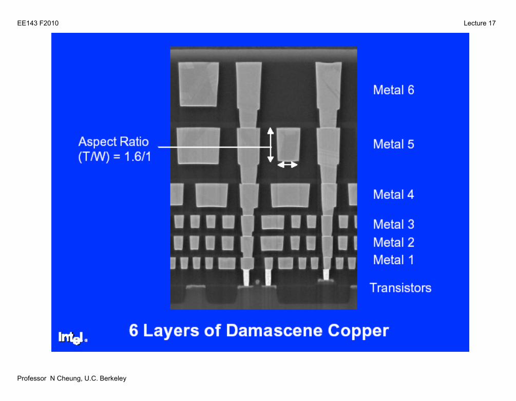
Metal 1 (copper)
Interlevel dielectric (ILD)
Silicon
Via (tungsten)
Metal 3 (copper)
Metal 5 (copper)
Passivation
Tungsten Plug to Si
Professor N Cheung, U.C. Berkeley
Lecture 17EE143 F2010
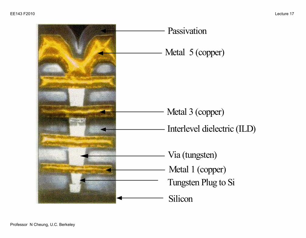
“Caps” and “Plugs”
The plug material can be same as interconnect material (e.g. Cu)or different material (e.g. W)
oxide oxide
Professor N Cheung, U.C. Berkeley
Lecture 17EE143 F2010
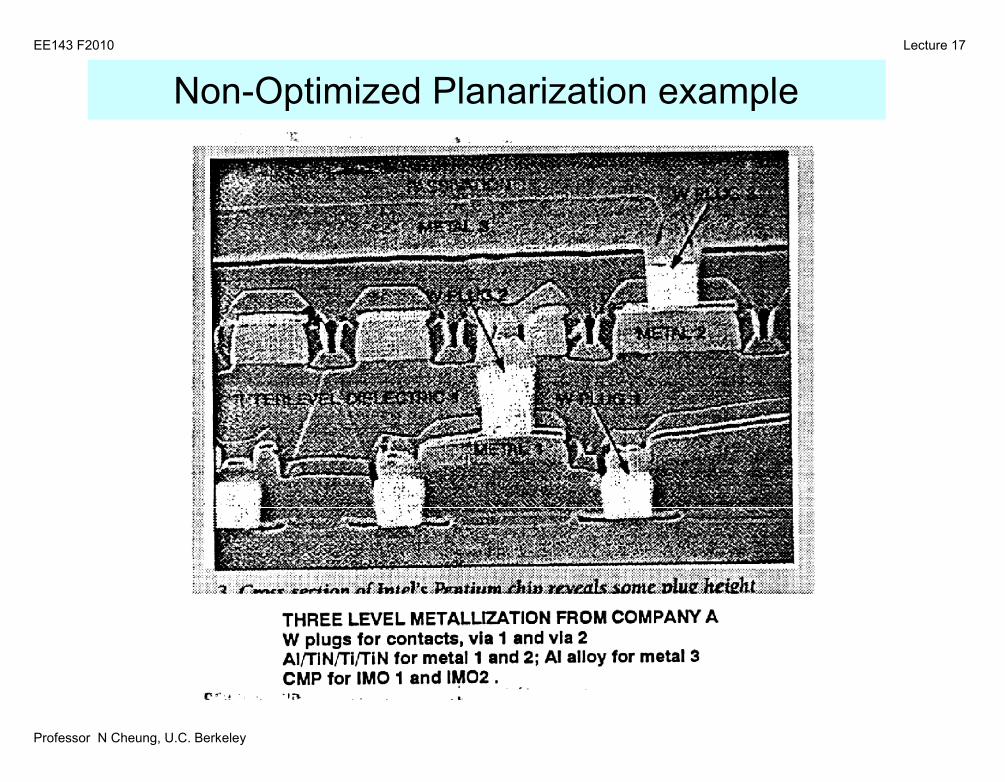
Non-Optimized Planarization example
Professor N Cheung, U.C. Berkeley
Lecture 17EE143 F2010
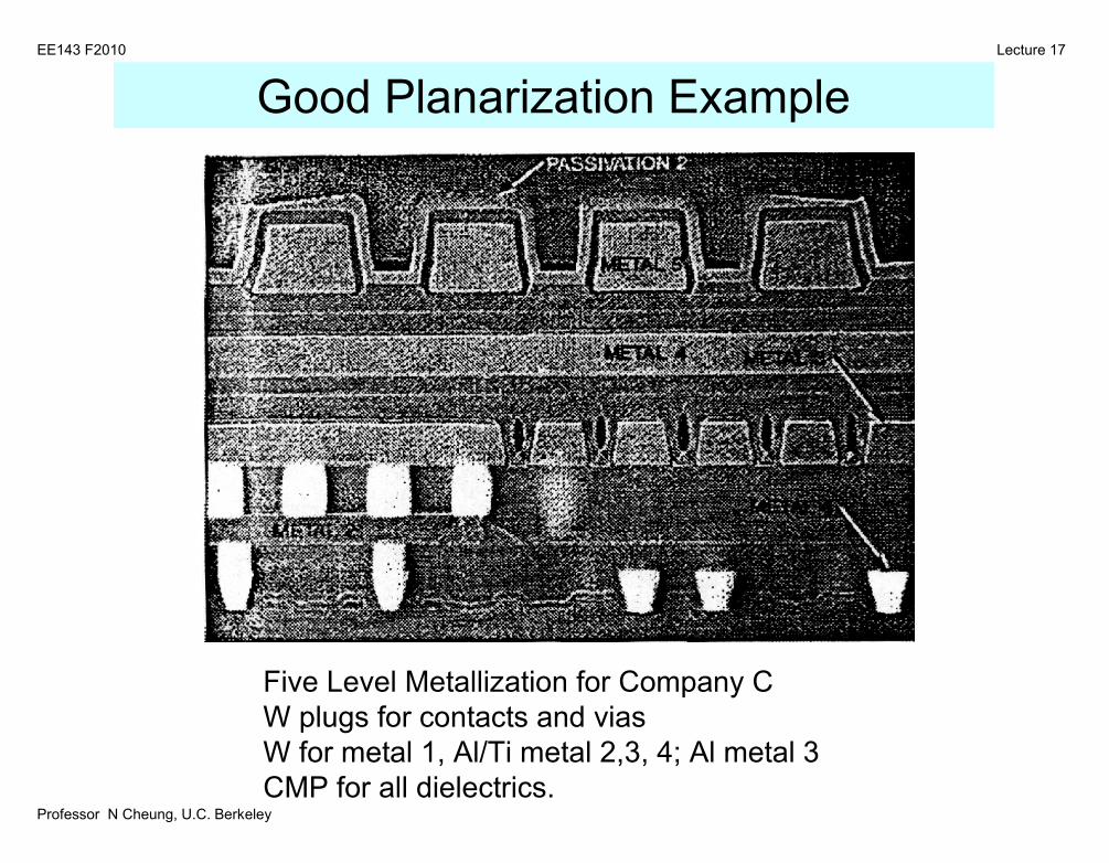
Five Level Metallization for Company CW plugs for contacts and viasW for metal 1, Al/Ti metal 2,3, 4; Al metal 3CMP for all dielectrics.
Good Planarization Example
Professor N Cheung, U.C. Berkeley
Lecture 17EE143 F2010
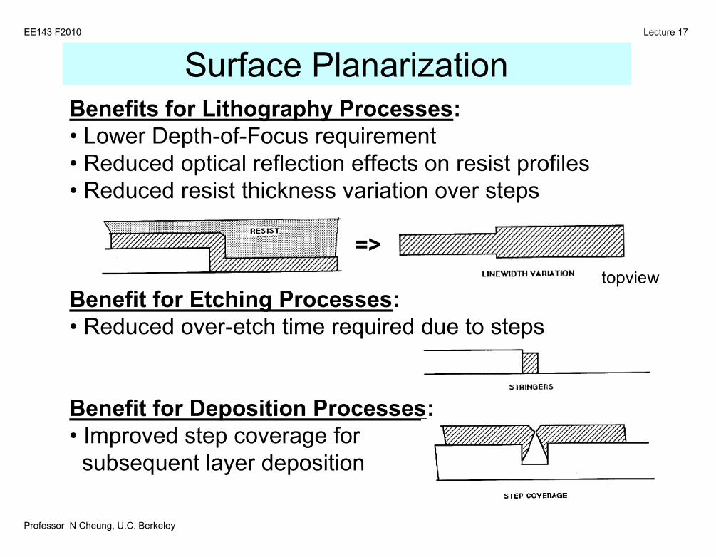
Benefits for Lithography Processes:• Lower Depth-of-Focus requirement• Reduced optical reflection effects on resist profiles• Reduced resist thickness variation over steps
=>
Benefit for Etching Processes:• Reduced over-etch time required due to steps
Benefit for Deposition Processes:• Improved step coverage for
subsequent layer deposition
topview
Surface Planarization
Professor N Cheung, U.C. Berkeley
Lecture 17EE143 F2010
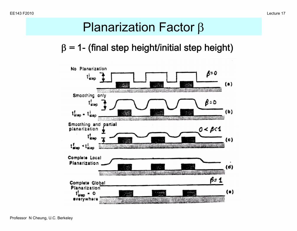
= 1- (final step height/initial step height)
Planarization Factor
Professor N Cheung, U.C. Berkeley
Lecture 17EE143 F2010
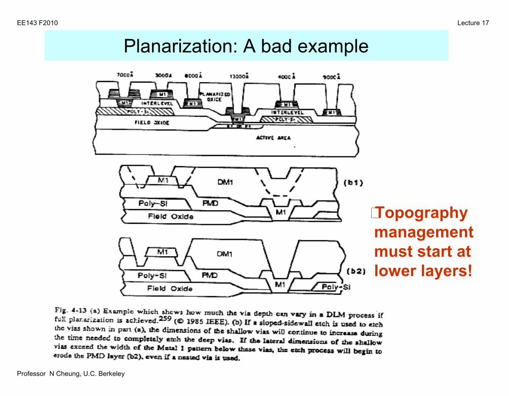
• Topographymanagementmust start atlower layers!
Planarization: A bad example
Professor N Cheung, U.C. Berkeley
Lecture 17EE143 F2010
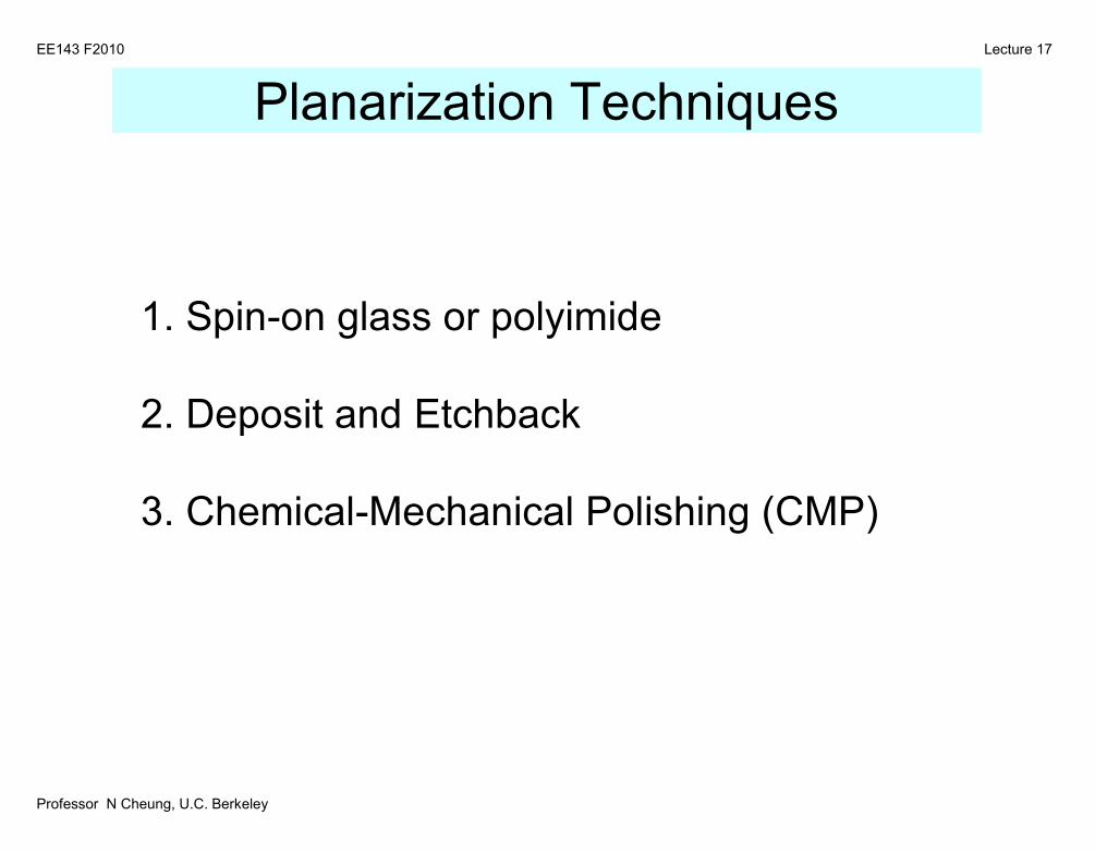
1. Spin-on glass or polyimide
2. Deposit and Etchback
3. Chemical-Mechanical Polishing (CMP)
Planarization Techniques
Professor N Cheung, U.C. Berkeley
Lecture 17EE143 F2010
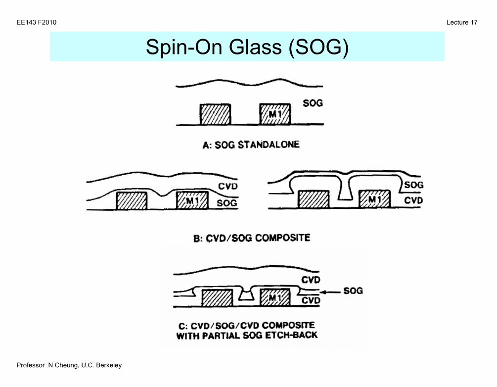
Spin-On Glass (SOG)
Professor N Cheung, U.C. Berkeley
Lecture 17EE143 F2010
SOG Annealing
• Cure:• 400-500oC -> inorganic backbone polymer
– exact composition depends on SOG type• 800-1100oC -> densified glass (inorganic SOGs)• can be performed in N2, O2 or steam
– steam allows densification to occur at lower– temperatures
Professor N Cheung, U.C. Berkeley
Lecture 17EE143 F2010
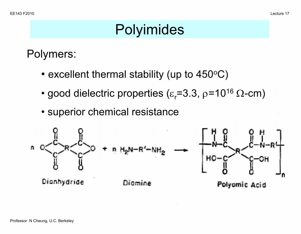
Polymers:
• excellent thermal stability (up to 450oC)
• good dielectric properties (r=3.3, =1016 -cm)
• superior chemical resistance
Polyimides
Professor N Cheung, U.C. Berkeley
Lecture 17EE143 F2010
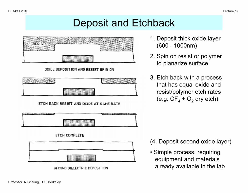
1. Deposit thick oxide layer(600 - 1000nm)
2. Spin on resist or polymerto planarize surface
3. Etch back with a processthat has equal oxide andresist/polymer etch rates(e.g. CF4 + O2 dry etch)
(4. Deposit second oxide layer)
• Simple process, requiringequipment and materialsalready available in the lab
Deposit and Etchback
Professor N Cheung, U.C. Berkeley
Lecture 17EE143 F2010
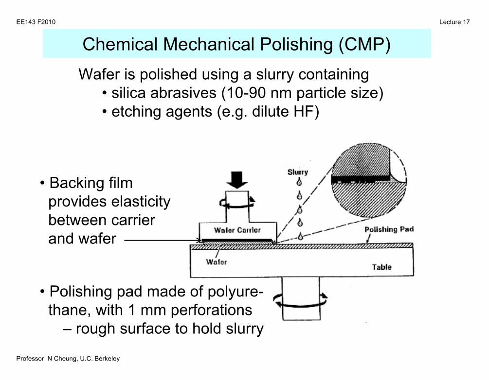
Wafer is polished using a slurry containing• silica abrasives (10-90 nm particle size)• etching agents (e.g. dilute HF)
• Backing filmprovides elasticitybetween carrierand wafer
• Polishing pad made of polyure-thane, with 1 mm perforations
– rough surface to hold slurry
Chemical Mechanical Polishing (CMP)
Professor N Cheung, U.C. Berkeley
Lecture 17EE143 F2010
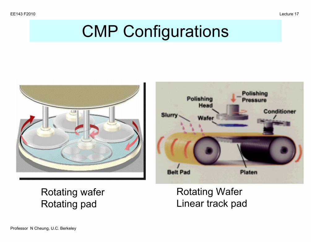
CMP Configurations
Rotating waferRotating pad
Rotating WaferLinear track pad
Professor N Cheung, U.C. Berkeley
Lecture 17EE143 F2010
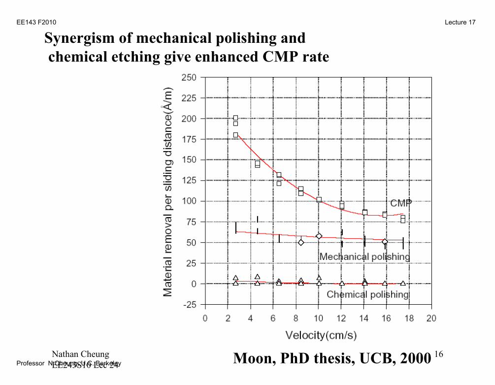
Nathan CheungEE243S10 Lec 24
16
Synergism of mechanical polishing andchemical etching give enhanced CMP rate
Moon, PhD thesis, UCB, 2000
Professor N Cheung, U.C. Berkeley
Lecture 17EE143 F2010
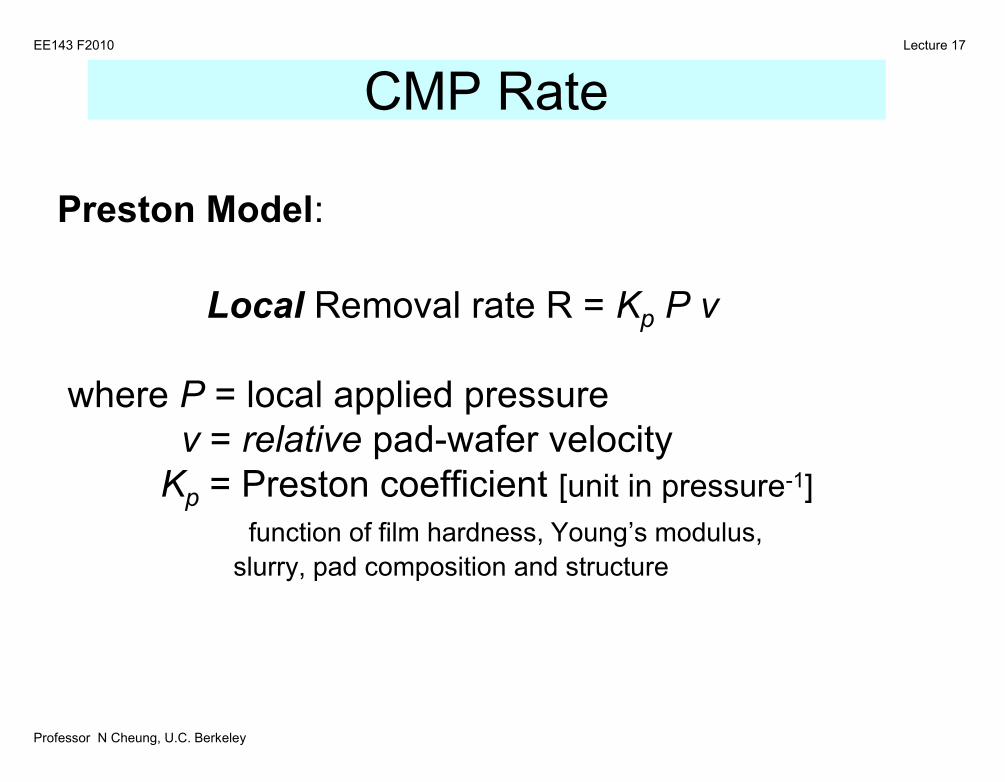
Preston Model:
Local Removal rate R = Kp P v
where P = local applied pressurev = relative pad-wafer velocity
Kp = Preston coefficient [unit in pressure-1]function of film hardness, Young’s modulus,
slurry, pad composition and structure
CMP Rate
Professor N Cheung, U.C. Berkeley
Lecture 17EE143 F2010
Nathan CheungEE243S10 Lec 24
18
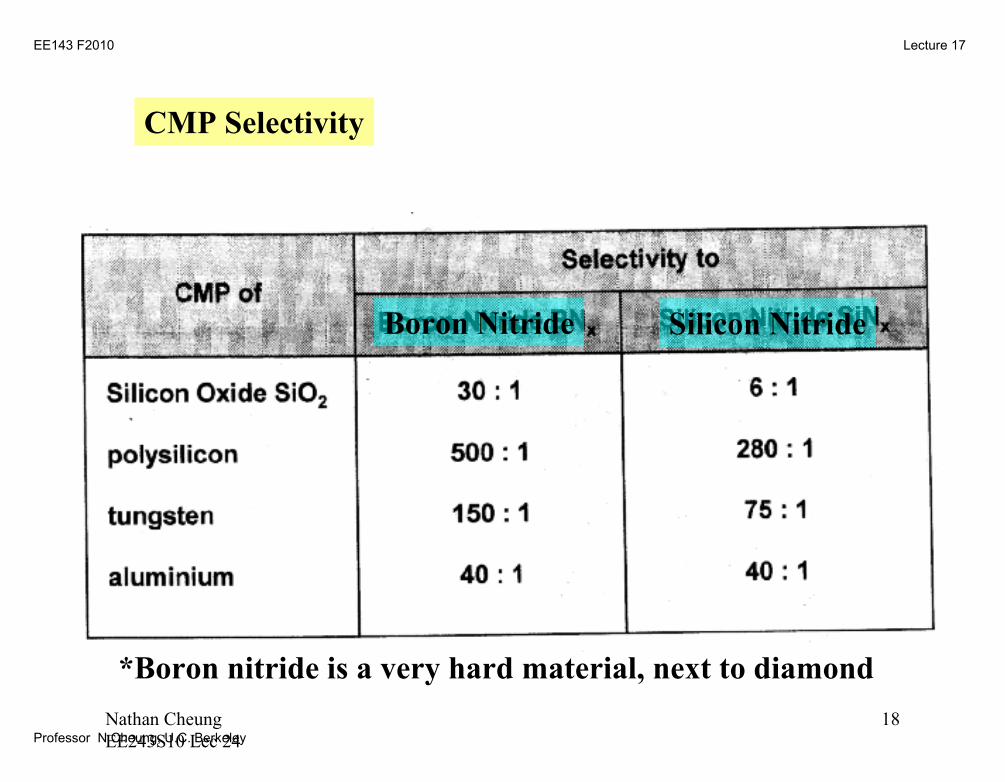
CMP Selectivity
Boron Nitride Silicon Nitride
*Boron nitride is a very hard material, next to diamond
Professor N Cheung, U.C. Berkeley
Lecture 17EE143 F2010
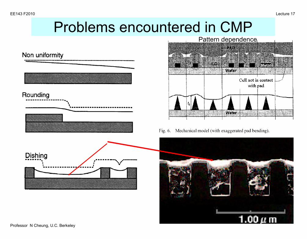
Pattern dependenceProblems encountered in CMP
Professor N Cheung, U.C. Berkeley
Lecture 17EE143 F2010
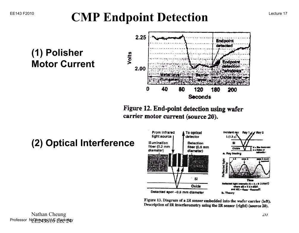
Nathan CheungEE243S10 Lec 24
20
(1) PolisherMotor Current
(2) Optical Interference
CMP Endpoint Detection
Professor N Cheung, U.C. Berkeley
Lecture 17EE143 F2010
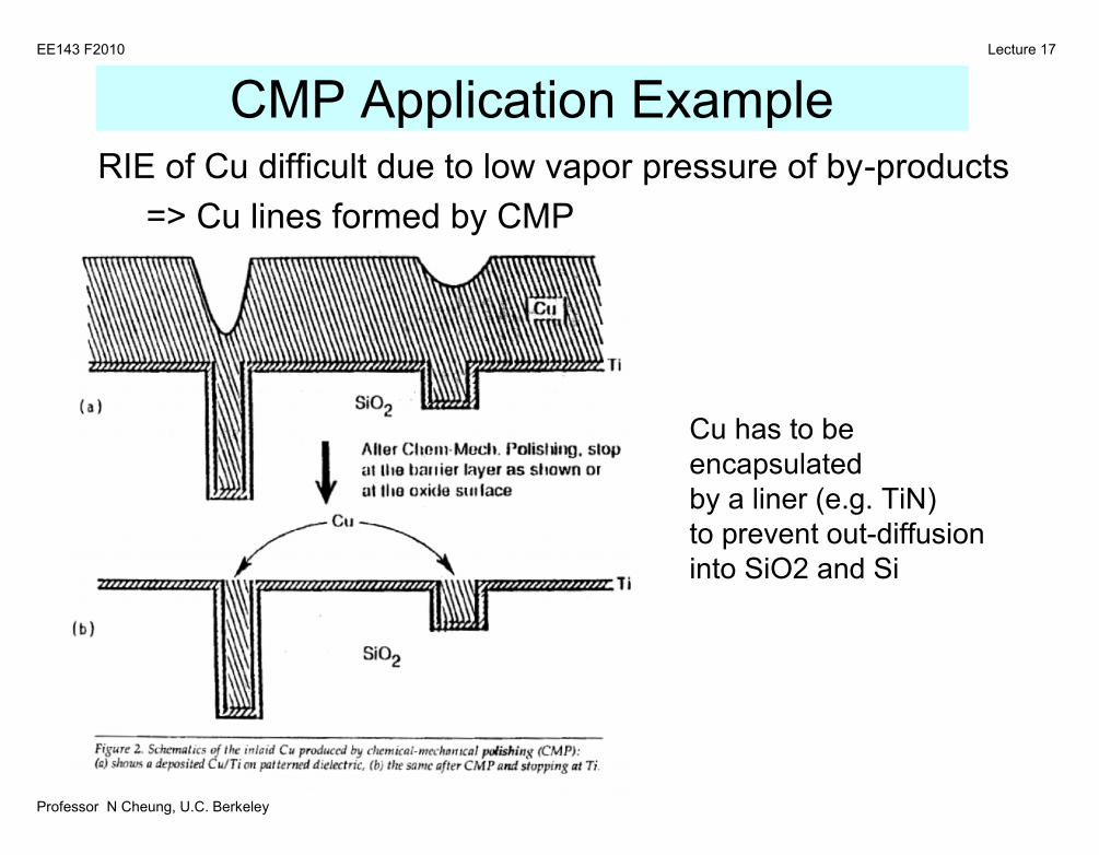
RIE of Cu difficult due to low vapor pressure of by-products=> Cu lines formed by CMP
Cu has to beencapsulatedby a liner (e.g. TiN)to prevent out-diffusioninto SiO2 and Si
CMP Application Example
Professor N Cheung, U.C. Berkeley
Lecture 17EE143 F2010
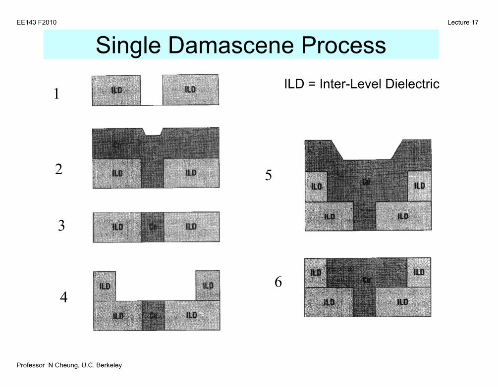
1
2
3
4
5
6
ILD = Inter-Level Dielectric
Single Damascene Process

Professor N Cheung, U.C. Berkeley
Lecture 17EE143 F2010
Cu
Dual Damascene Cu Metallization with Diffusion Barrier
Professor N Cheung, U.C. Berkeley
Lecture 17EE143 F2010
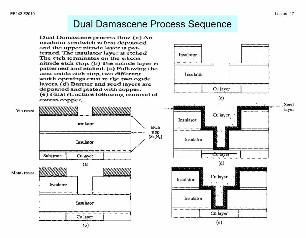
Dual Damascene Process Sequence
Professor N Cheung, U.C. Berkeley
Lecture 17EE143 F2010
Professor N Cheung, U.C. Berkeley
Lecture 17EE143 F2010
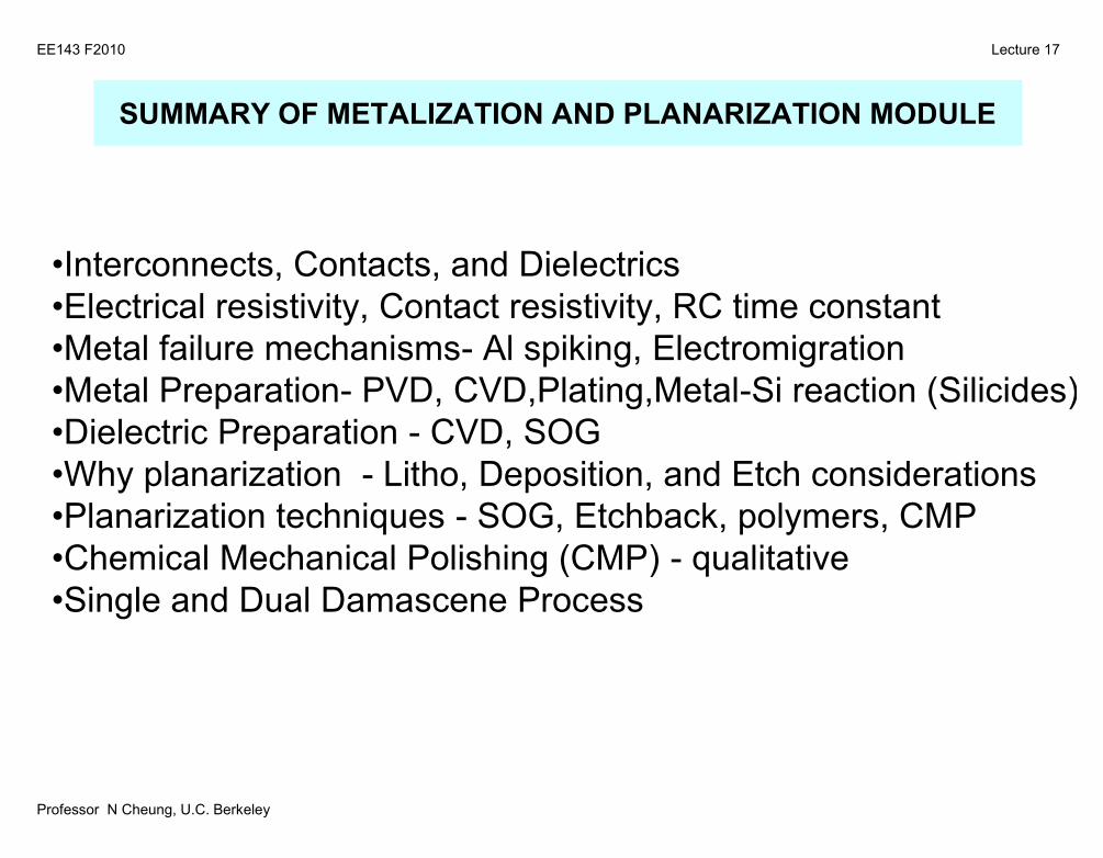
SUMMARY OF METALIZATION AND PLANARIZATION MODULE
•Interconnects, Contacts, and Dielectrics•Electrical resistivity, Contact resistivity, RC time constant•Metal failure mechanisms- Al spiking, Electromigration•Metal Preparation- PVD, CVD,Plating,Metal-Si reaction (Silicides)•Dielectric Preparation - CVD, SOG•Why planarization - Litho, Deposition, and Etch considerations•Planarization techniques - SOG, Etchback, polymers, CMP•Chemical Mechanical Polishing (CMP) - qualitative•Single and Dual Damascene Process