Embed Size (px)
Citation preview
Integration -from the view point of electronics-
ver 0 2014.05.12 M.T. ver0.1 2014.05.21 M.T.
ver1.0 2014.05.30 M.T. F.A. I.A. S.T. Y.U. G.V. et al.
Recommendation for each sub-detector has already been described in ref[0] in detail.Figures and texts from ref [0,1,2,3] are protected by copyright. If you want to use them, please contact with authors.
This document describes “integration guideline for outside of sub-detectors and their interconnections. It does never compel sub-detector group to follow the guideline for the inside of sub-detector.
Outline• Guideline
• General, sub-detector level, interconnection
• Basics of electromagnetic compatibility(EMC)
• EMC, Basic treatment and its detail
• Other tips
• Reference
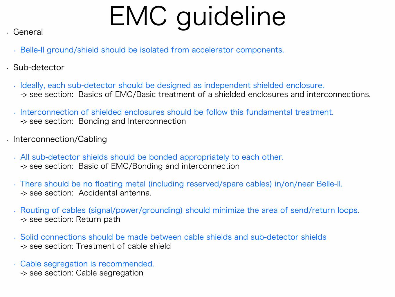
EMC guideline• General
• Belle-II ground/shield should be isolated from accelerator components.
• Sub-detector
• Ideally, each sub-detector should be designed as independent shielded enclosure. -> see section: Basics of EMC/Basic treatment of a shielded enclosures and interconnections.
• Interconnection of shielded enclosures should be follow this fundamental treatment. -> see section: Bonding and Interconnection
• Interconnection/Cabling
• All sub-detector shields should be bonded appropriately to each other. -> see section: Basic of EMC/Bonding and interconnection
• There should be no floating metal (including reserved/spare cables) in/on/near Belle-II. -> see section: Accidental antenna.
• Routing of cables (signal/power/grounding) should minimize the area of send/return loops. -> see section: Return path
• Solid connections should be made between cable shields and sub-detector shields -> see section: Treatment of cable shield
• Cable segregation is recommended. -> see section: Cable segregation
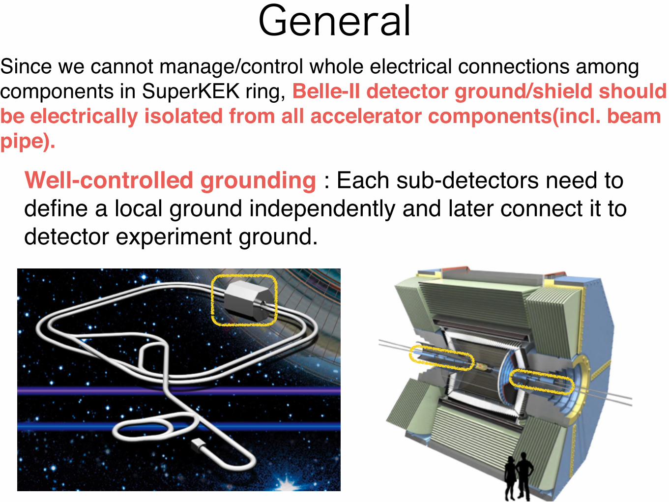
General
Well-controlled grounding : Each sub-detectors need to define a local ground independently and later connect it to detector experiment ground.
Since we cannot manage/control whole electrical connections among components in SuperKEK ring, Belle-II detector ground/shield should be electrically isolated from all accelerator components(incl. beam pipe).
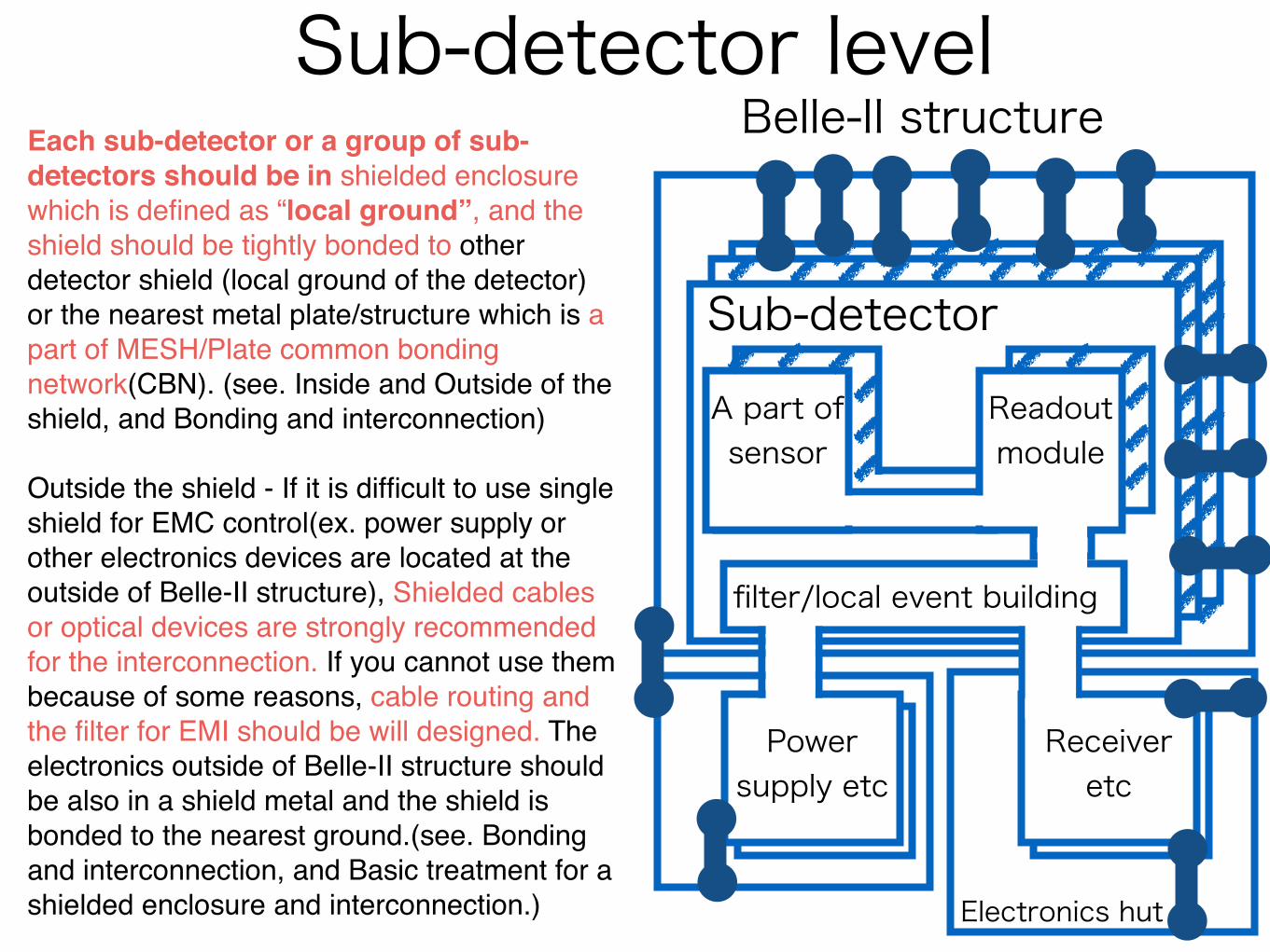
Sub-detector levelEach sub-detector or a group of sub-detectors should be in shielded enclosure which is defined as “local ground”, and the shield should be tightly bonded to other detector shield (local ground of the detector) or the nearest metal plate/structure which is a part of MESH/Plate common bonding network(CBN). (see. Inside and Outside of the shield, and Bonding and interconnection)!!Outside the shield - If it is difficult to use single shield for EMC control(ex. power supply or other electronics devices are located at the outside of Belle-II structure), Shielded cables or optical devices are strongly recommended for the interconnection. If you cannot use them because of some reasons, cable routing and the filter for EMI should be will designed. The electronics outside of Belle-II structure should be also in a shield metal and the shield is bonded to the nearest ground.(see. Bonding and interconnection, and Basic treatment for a shielded enclosure and interconnection.)
Readout module
A part of sensor
filter/local event building
Power supply etc
Receiver etc
Sub-detector
Belle-II structure
Electronics hut
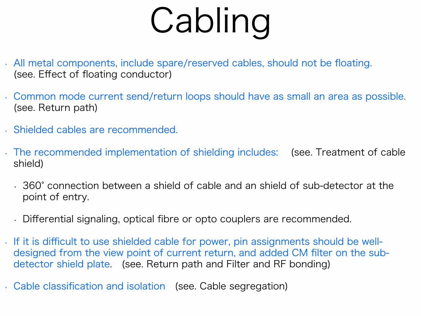
Cabling• All metal components, include spare/reserved cables, should not be floating. (see. Effect of floating conductor)
• Common mode current send/return loops should have as small an area as possible. (see. Return path)
• Shielded cables are recommended.
• The recommended implementation of shielding includes: (see. Treatment of cable shield)
• 360° connection between a shield of cable and an shield of sub-detector at the point of entry.
• Differential signaling, optical fibre or opto couplers are recommended.
• If it is difficult to use shielded cable for power, pin assignments should be well-designed from the view point of current return, and added CM filter on the sub-detector shield plate. (see. Return path and Filter and RF bonding)
• Cable classification and isolation (see. Cable segregation)
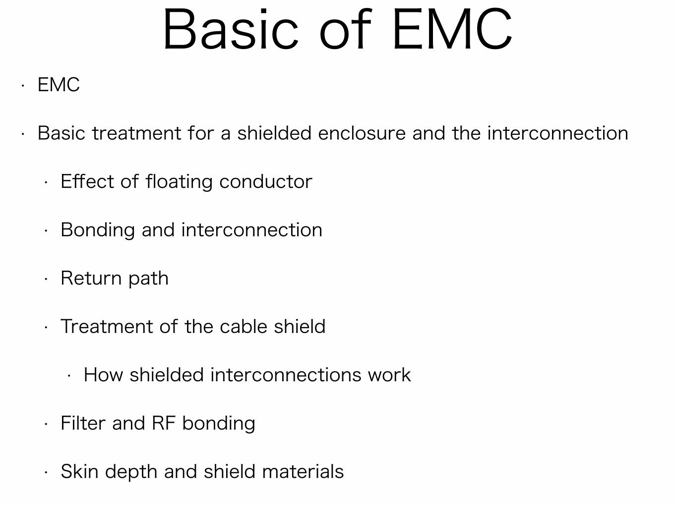
Basic of EMC• EMC
• Basic treatment for a shielded enclosure and the interconnection
• Effect of floating conductor
• Bonding and interconnection
• Return path
• Treatment of the cable shield
• How shielded interconnections work
• Filter and RF bonding
• Skin depth and shield materials
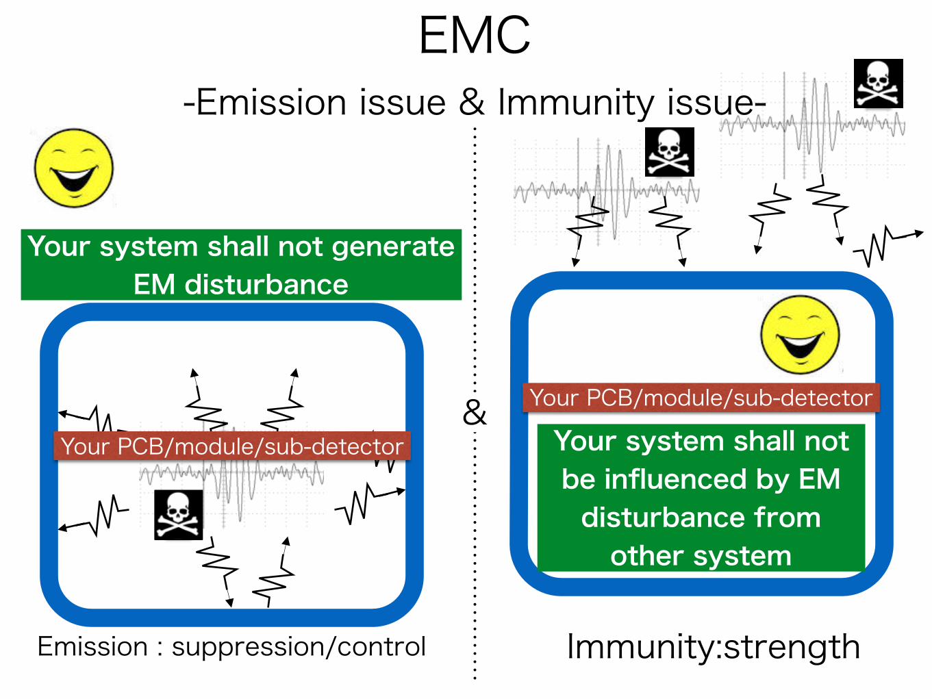
Emission : suppression/control Immunity:strength
Your PCB/module/sub-detector&
EMC -Emission issue & Immunity issue-
Your system shall not generate EM disturbance
Your system shall not be influenced by EM disturbance from other system
Your PCB/module/sub-detector
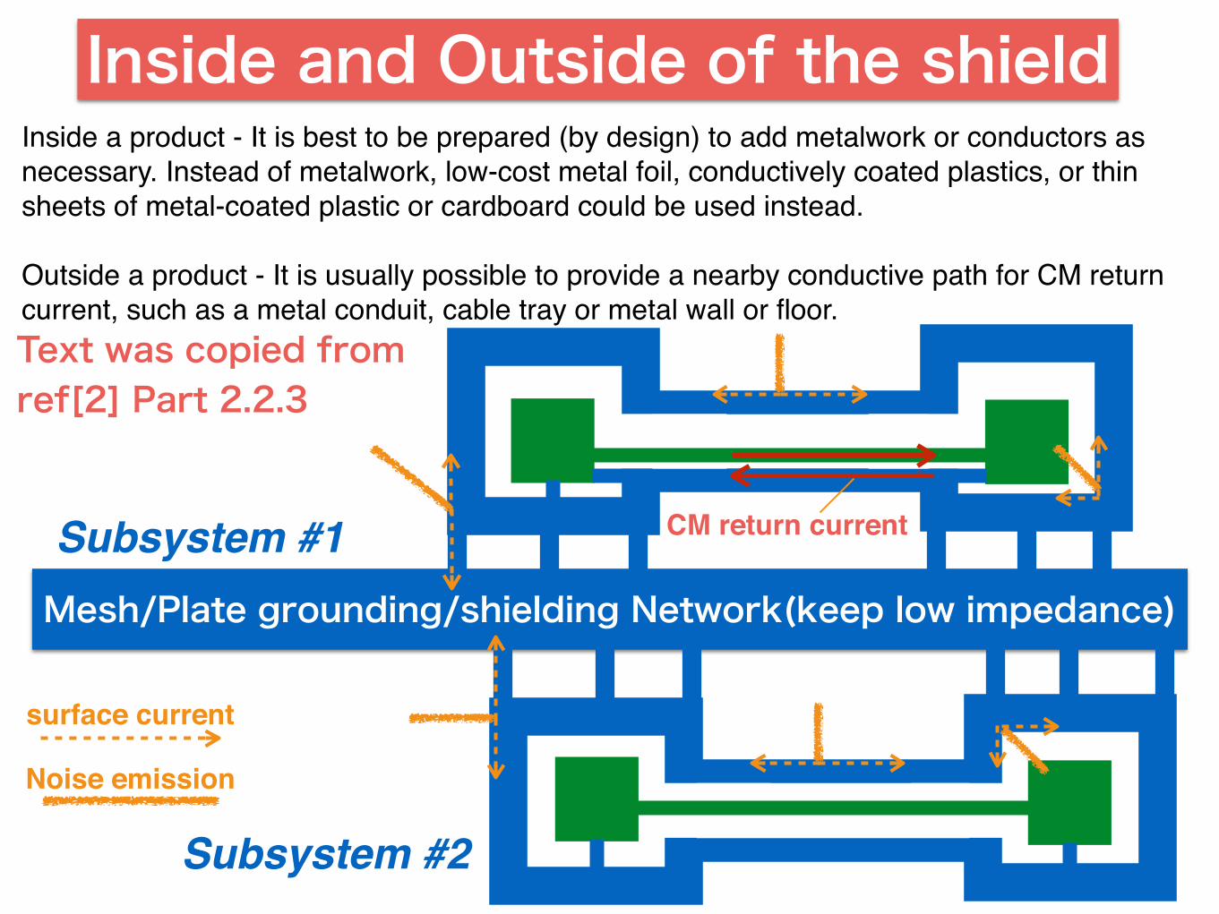
Inside a product - It is best to be prepared (by design) to add metalwork or conductors as necessary. Instead of metalwork, low-cost metal foil, conductively coated plastics, or thin sheets of metal-coated plastic or cardboard could be used instead.!!Outside a product - It is usually possible to provide a nearby conductive path for CM return current, such as a metal conduit, cable tray or metal wall or floor.
Inside and Outside of the shield
Mesh/Plate grounding/shielding Network(keep low impedance)
Subsystem #1
Subsystem #2
surface current
Noise emission
CM return current
Text was copied from ref[2] Part 2.2.3
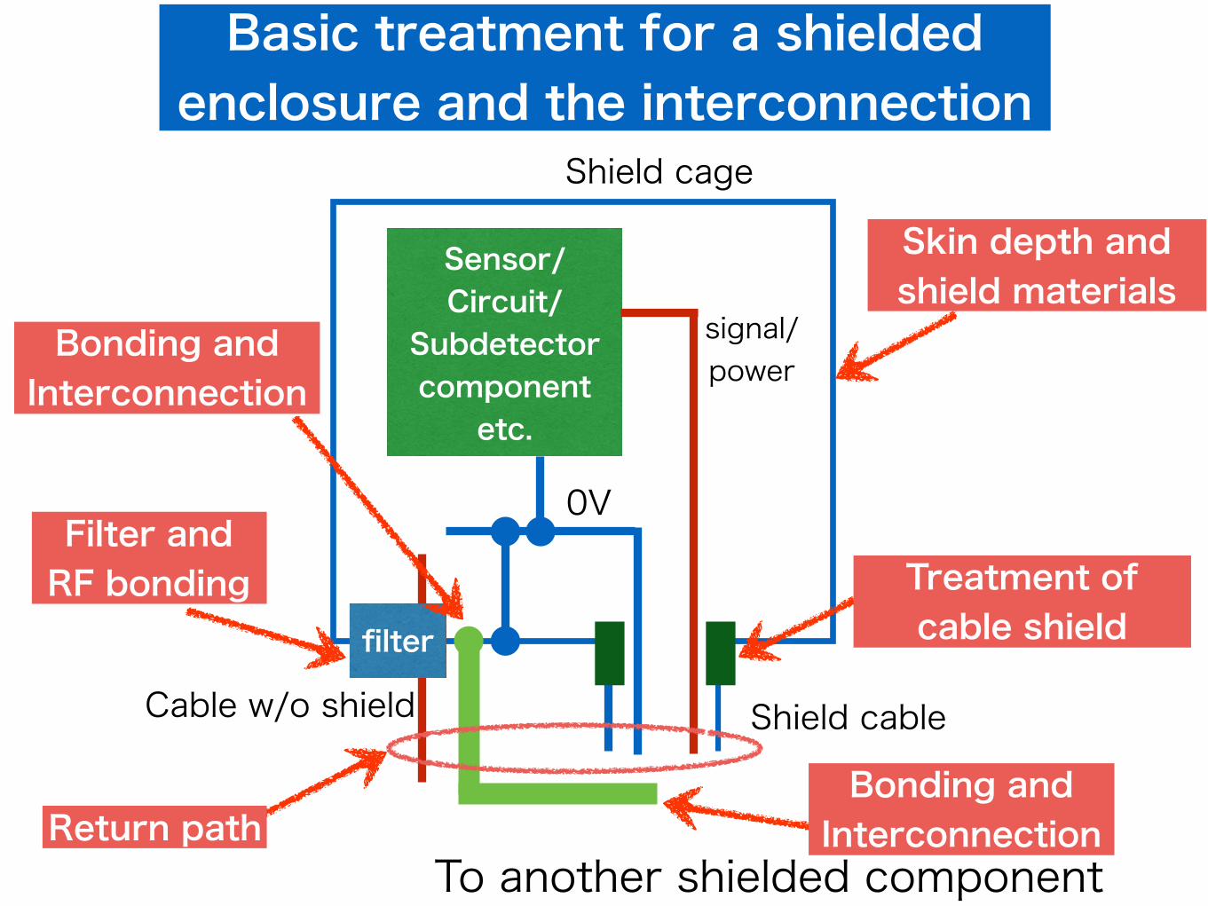
Basic treatment for a shielded enclosure and the interconnection
Sensor/Circuit/
Subdetector component
etc.
0V
To another shielded component
Shield cage
Shield cable
filter
Cable w/o shield
Skin depth and shield materials
Return path
Treatment of cable shield
Bonding and Interconnection
Filter and RF bonding
signal/power
Bonding and Interconnection
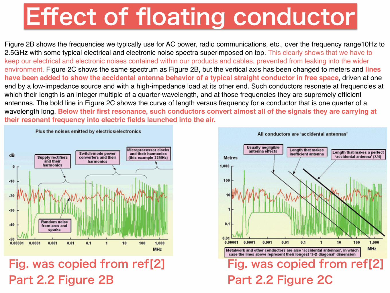
Figure 2B shows the frequencies we typically use for AC power, radio communications, etc., over the frequency range10Hz to 2.5GHz with some typical electrical and electronic noise spectra superimposed on top. This clearly shows that we have to keep our electrical and electronic noises contained within our products and cables, prevented from leaking into the wider environment. Figure 2C shows the same spectrum as Figure 2B, but the vertical axis has been changed to meters and lines have been added to show the accidental antenna behavior of a typical straight conductor in free space, driven at one end by a low-impedance source and with a high-impedance load at its other end. Such conductors resonate at frequencies at which their length is an integer multiple of a quarter-wavelength, and at those frequencies they are supremely efficient antennas. The bold line in Figure 2C shows the curve of length versus frequency for a conductor that is one quarter of a wavelength long. Below their first resonance, such conductors convert almost all of the signals they are carrying at their resonant frequency into electric fields launched into the air.
Effect of floating conductor
Fig. was copied from ref[2] Part 2.2 Figure 2B
Fig. was copied from ref[2] Part 2.2 Figure 2C
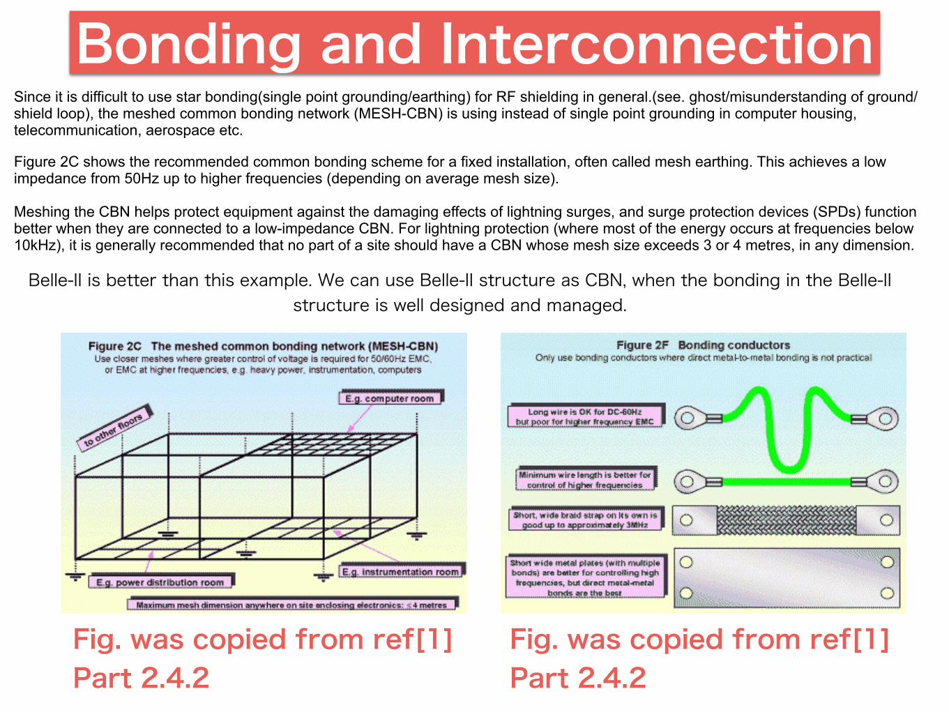
Since it is difficult to use star bonding(single point grounding/earthing) for RF shielding in general.(see. ghost/misunderstanding of ground/shield loop), the meshed common bonding network (MESH-CBN) is using instead of single point grounding in computer housing, telecommunication, aerospace etc.
Figure 2C shows the recommended common bonding scheme for a fixed installation, often called mesh earthing. This achieves a low impedance from 50Hz up to higher frequencies (depending on average mesh size). !Meshing the CBN helps protect equipment against the damaging effects of lightning surges, and surge protection devices (SPDs) function better when they are connected to a low-impedance CBN. For lightning protection (where most of the energy occurs at frequencies below 10kHz), it is generally recommended that no part of a site should have a CBN whose mesh size exceeds 3 or 4 metres, in any dimension.
Bonding and Interconnection
Fig. was copied from ref[1] Part 2.4.2
Fig. was copied from ref[1] Part 2.4.2
Belle-II is better than this example. We can use Belle-II structure as CBN, when the bonding in the Belle-II structure is well designed and managed.
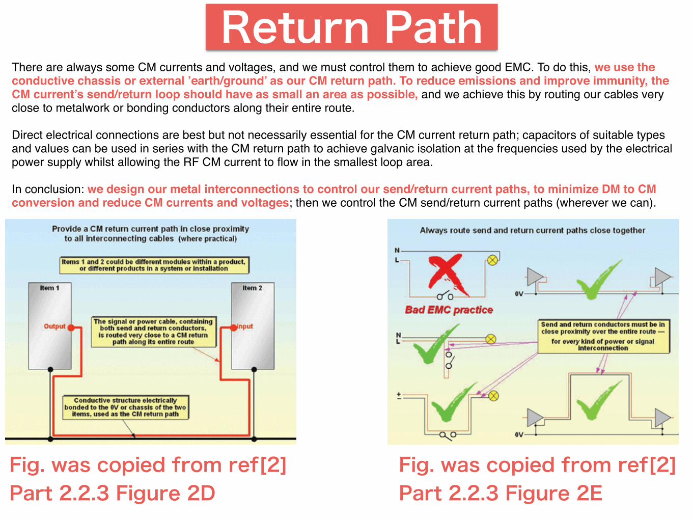
There are always some CM currents and voltages, and we must control them to achieve good EMC. To do this, we use the conductive chassis or external ’earth/ground’ as our CM return path. To reduce emissions and improve immunity, the CM current’s send/return loop should have as small an area as possible, and we achieve this by routing our cables very close to metalwork or bonding conductors along their entire route. !!Direct electrical connections are best but not necessarily essential for the CM current return path; capacitors of suitable types and values can be used in series with the CM return path to achieve galvanic isolation at the frequencies used by the electrical power supply whilst allowing the RF CM current to flow in the smallest loop area.!!In conclusion: we design our metal interconnections to control our send/return current paths, to minimize DM to CM conversion and reduce CM currents and voltages; then we control the CM send/return current paths (wherever we can).
Return Path
Fig. was copied from ref[2] Part 2.2.3 Figure 2D
Fig. was copied from ref[2] Part 2.2.3 Figure 2E
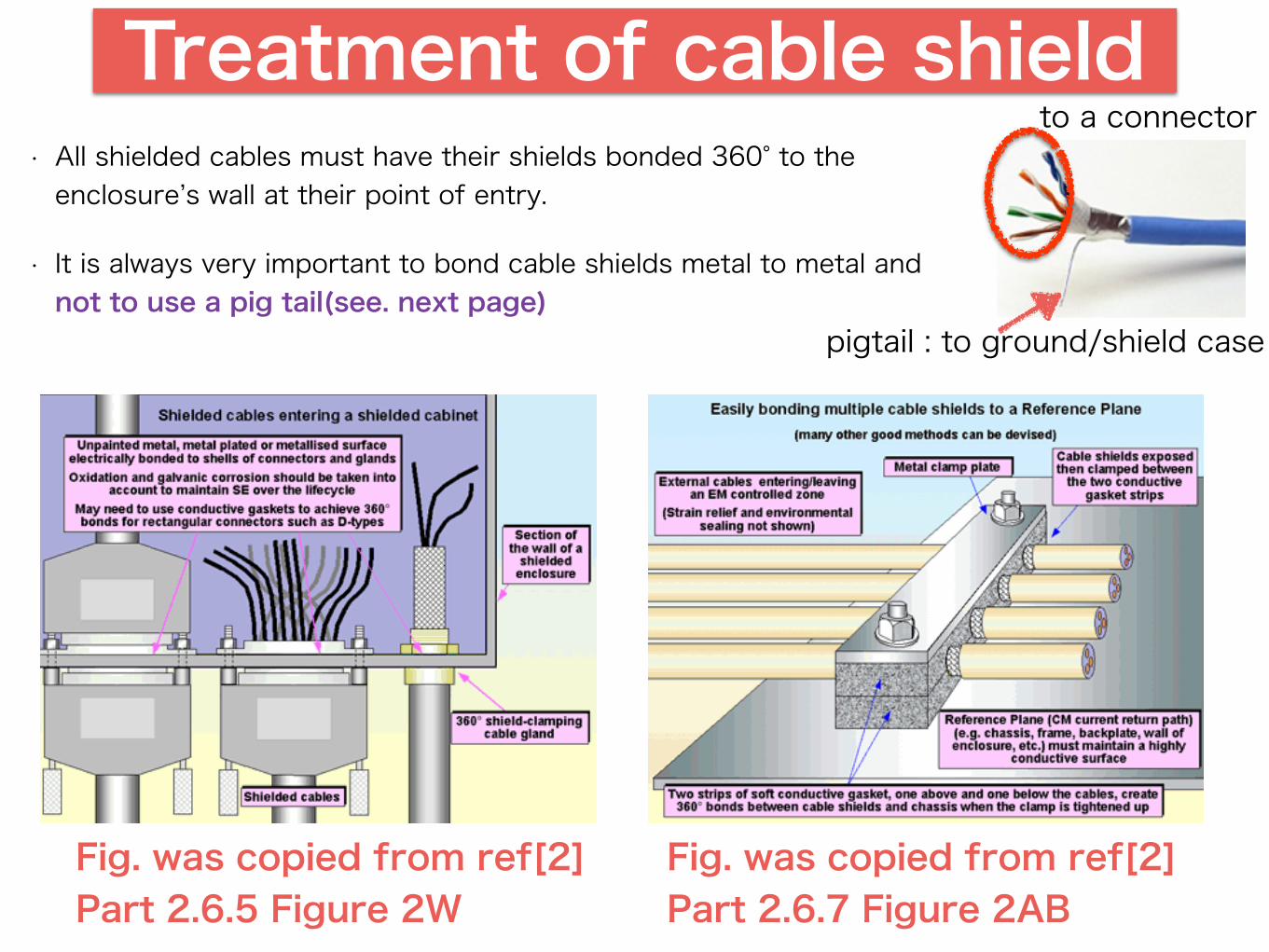
Treatment of cable shield• All shielded cables must have their shields bonded 360° to the enclosure’s wall at their point of entry.
• It is always very important to bond cable shields metal to metal and not to use a pig tail(see. next page)
Fig. was copied from ref[2] Part 2.6.5 Figure 2W
Fig. was copied from ref[2] Part 2.6.7 Figure 2AB
to a connector
pigtail : to ground/shield case
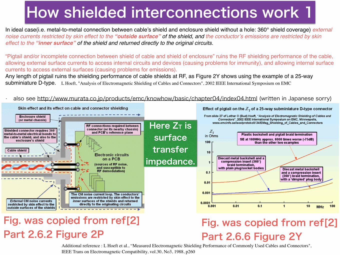
In ideal case(i.e. metal-to-metal connection between cable’s shield and enclosure shield without a hole: 360° shield coverage) external noise currents restricted by skin effect to the “outside surface” of the shield, and the conductor’s emissions are restricted by skin effect to the “inner surface” of the shield and returned directly to the original circuits.!!“Pigtail and/or incomplete connection between shield of cable and shield of enclosure” ruins the RF shielding performance of the cable, allowing external surface currents to access internal circuits and devices (causing problems for immunity), and allowing internal surface currents to access external surfaces (causing problems for emissions).!Any length of pigtail ruins the shielding performance of cable shields at RF, as Figure 2Y shows using the example of a 25-way subminiature D-type.!
• also see http://www.murata.co.jp/products/emc/knowhow/basic/chapter04/index04.html (written in Japanese sorry)
How shielded interconnections work 1
Fig. was copied from ref[2] Part 2.6.6 Figure 2Y
Fig. was copied from ref[2] Part 2.6.2 Figure 2P
L Hoeft, "Analysis of Electromagnetic Shielding of Cables and Connectors", 2002 IEEE International Symposium on EMC
Additional reference : L Hoeft et al., “Measured Electromagnetic Shielding Performance of Commonly Used Cables and Connectors", IEEE Trans on Electromagnetic Compatibility, vol.30, No3, 1988, p260
Here ZT is surface transfer impedance.
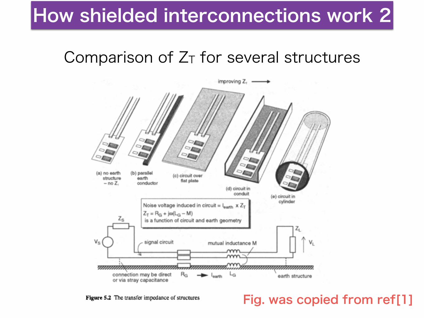
How shielded interconnections work 2
Fig. was copied from ref[1]
Comparison of ZT for several structures
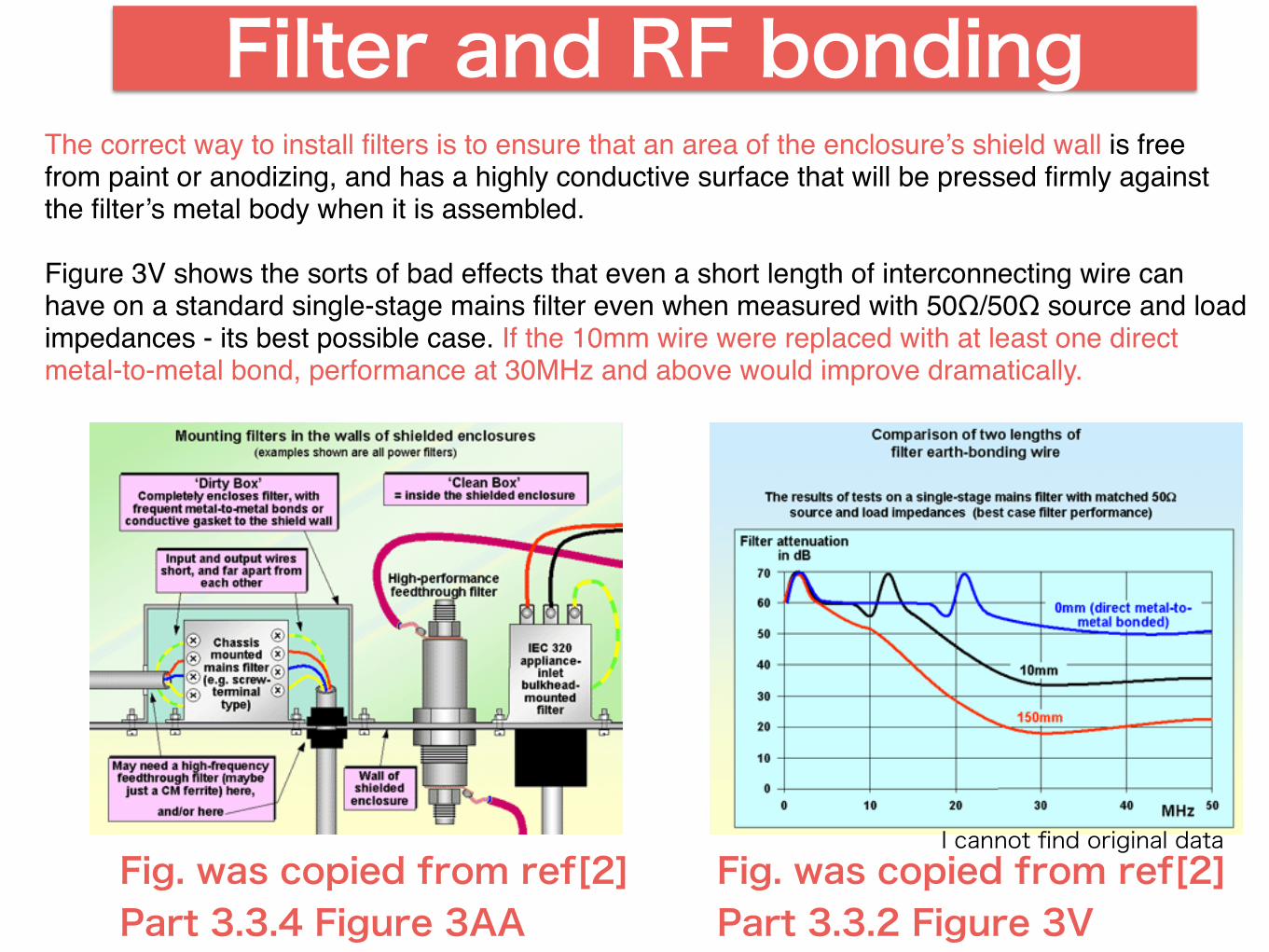
The correct way to install filters is to ensure that an area of the enclosure’s shield wall is free from paint or anodizing, and has a highly conductive surface that will be pressed firmly against the filter’s metal body when it is assembled.!!Figure 3V shows the sorts of bad effects that even a short length of interconnecting wire can have on a standard single-stage mains filter even when measured with 50Ω/50Ω source and load impedances - its best possible case. If the 10mm wire were replaced with at least one direct metal-to-metal bond, performance at 30MHz and above would improve dramatically.
Filter and RF bonding
Fig. was copied from ref[2] Part 3.3.4 Figure 3AA
Fig. was copied from ref[2] Part 3.3.2 Figure 3V
I cannot find original data
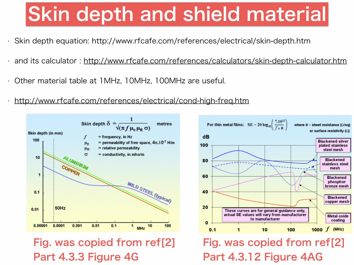
Skin depth-Chapter 4-• Skin depth equation: http://www.rfcafe.com/references/electrical/skin-depth.htm
• and its calculator : http://www.rfcafe.com/references/calculators/skin-depth-calculator.htm
• Other material table at 1MHz, 10MHz, 100MHz are useful.
• http://www.rfcafe.com/references/electrical/cond-high-freq.htm
Skin depth and shield material
Fig. was copied from ref[2] Part 4.3.3 Figure 4G
Fig. was copied from ref[2] Part 4.3.12 Figure 4AG
Tips
• Differential Mode(DM) and Common Mode(CM)
• Ghost/misunderstanding of ground/shield loop.
• Cable segregation
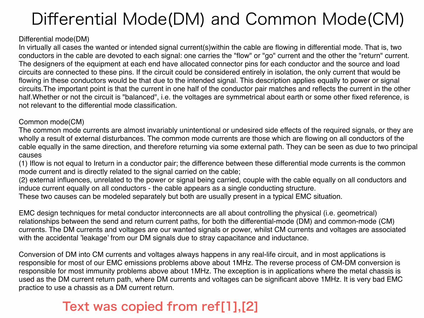
Differential Mode(DM) and Common Mode(CM)Differential mode(DM)!In virtually all cases the wanted or intended signal current(s)within the cable are flowing in differential mode. That is, two conductors in the cable are devoted to each signal: one carries the "flow" or "go" current and the other the "return" current. The designers of the equipment at each end have allocated connector pins for each conductor and the source and load circuits are connected to these pins. If the circuit could be considered entirely in isolation, the only current that would be flowing in these conductors would be that due to the intended signal. This description applies equally to power or signal circuits.The important point is that the current in one half of the conductor pair matches and reflects the current in the other half.Whether or not the circuit is "balanced", i.e. the voltages are symmetrical about earth or some other fixed reference, is not relevant to the differential mode classification.!!Common mode(CM)!The common mode currents are almost invariably unintentional or undesired side effects of the required signals, or they are wholly a result of external disturbances. The common mode currents are those which are flowing on all conductors of the cable equally in the same direction, and therefore returning via some external path. They can be seen as due to two principal causes !(1) Iflow is not equal to Ireturn in a conductor pair; the difference between these differential mode currents is the common mode current and is directly related to the signal carried on the cable; !(2) external influences, unrelated to the power or signal being carried, couple with the cable equally on all conductors and induce current equally on all conductors - the cable appears as a single conducting structure. !These two causes can be modeled separately but both are usually present in a typical EMC situation.!!EMC design techniques for metal conductor interconnects are all about controlling the physical (i.e. geometrical) relationships between the send and return current paths, for both the differential-mode (DM) and common-mode (CM) currents. The DM currents and voltages are our wanted signals or power, whilst CM currents and voltages are associated with the accidental ’leakage’ from our DM signals due to stray capacitance and inductance. !!Conversion of DM into CM currents and voltages always happens in any real-life circuit, and in most applications is responsible for most of our EMC emissions problems above about 1MHz. The reverse process of CM-DM conversion is responsible for most immunity problems above about 1MHz. The exception is in applications where the metal chassis is used as the DM current return path, where DM currents and voltages can be significant above 1MHz. It is very bad EMC practice to use a chassis as a DM current return.
Text was copied from ref[1],[2]
Ghost/Misunderstanding of ground/shield loop
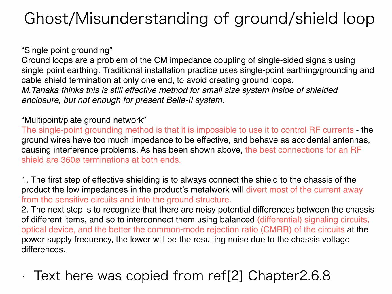
“Single point grounding”!Ground loops are a problem of the CM impedance coupling of single-sided signals using single point earthing. Traditional installation practice uses single-point earthing/grounding and cable shield termination at only one end, to avoid creating ground loops.!M.Tanaka thinks this is still effective method for small size system inside of shielded enclosure, but not enough for present Belle-II system.!!“Multipoint/plate ground network”!The single-point grounding method is that it is impossible to use it to control RF currents - the ground wires have too much impedance to be effective, and behave as accidental antennas, causing interference problems. As has been shown above, the best connections for an RF shield are 360ø terminations at both ends.!!1. The first step of effective shielding is to always connect the shield to the chassis of the product the low impedances in the product’s metalwork will divert most of the current away from the sensitive circuits and into the ground structure.!2. The next step is to recognize that there are noisy potential differences between the chassis of different items, and so to interconnect them using balanced (differential) signaling circuits, optical device, and the better the common-mode rejection ratio (CMRR) of the circuits at the power supply frequency, the lower will be the resulting noise due to the chassis voltage differences.!
• Text here was copied from ref[2] Chapter2.6.8
Cable segregation
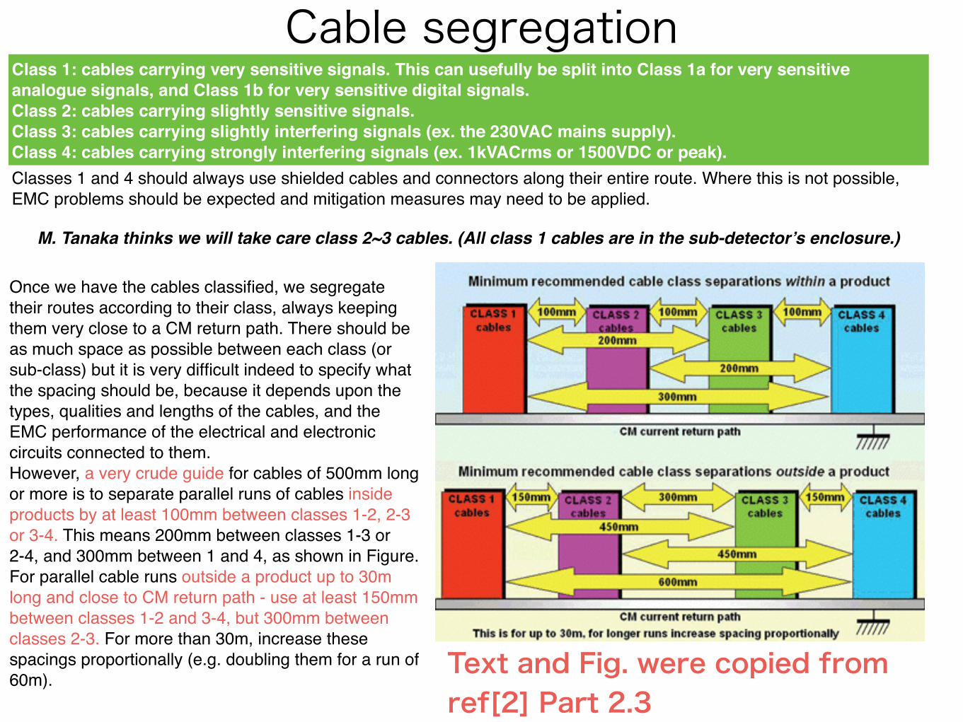
Once we have the cables classified, we segregate their routes according to their class, always keeping them very close to a CM return path. There should be as much space as possible between each class (or sub-class) but it is very difficult indeed to specify what the spacing should be, because it depends upon the types, qualities and lengths of the cables, and the EMC performance of the electrical and electronic circuits connected to them.!However, a very crude guide for cables of 500mm long or more is to separate parallel runs of cables inside products by at least 100mm between classes 1-2, 2-3 or 3-4. This means 200mm between classes 1-3 or 2-4, and 300mm between 1 and 4, as shown in Figure. For parallel cable runs outside a product up to 30m long and close to CM return path - use at least 150mm between classes 1-2 and 3-4, but 300mm between classes 2-3. For more than 30m, increase these spacings proportionally (e.g. doubling them for a run of 60m).!
Class 1: cables carrying very sensitive signals. This can usefully be split into Class 1a for very sensitive analogue signals, and Class 1b for very sensitive digital signals.!Class 2: cables carrying slightly sensitive signals.!Class 3: cables carrying slightly interfering signals (ex. the 230VAC mains supply).!Class 4: cables carrying strongly interfering signals (ex. 1kVACrms or 1500VDC or peak).Classes 1 and 4 should always use shielded cables and connectors along their entire route. Where this is not possible, EMC problems should be expected and mitigation measures may need to be applied.
Text and Fig. were copied from ref[2] Part 2.3
M. Tanaka thinks we will take care class 2~3 cables. (All class 1 cables are in the sub-detector’s enclosure.)
references• ref[0] “Grounding & EMC Committee review report”, Aug. 2013, F. Arteche et al.(Review Committee)(see. http://kds.kek.jp/getFile.py/access?contribId=5&resId=0&materialId=0&confId=13577)“Belle II:Grounding and Electronics integration Issues”, F. Arteche, B2GM, July 6-9, 2011, Nagoya, Japan. (see. http://www-esys.kek.jp/r-and-d/emc/emc-related-references)“EMC:Electronics system integration for HEP experiments” F. Arteche B2GM Nov 15-20, 2011, KEK, Japan. (see. http://www-esys.kek.jp/r-and-d/emc/emc-related-references) “EMC issues for cabling and racks layout design”, F. Arteche, B2GM, Mar4-7, 2013, KEK, Japan. (see. https://belle2.cc.kek.jp/~twiki/bin/view/Public/WebHome#review)“Grounding & EMC : Status and Plans”, F. Arteche, Belle II Focused Review, Sept. 9-10, 2013, KEK, Japan. (see. http://kds.kek.jp/conferenceDisplay.py?confId=13464)
• ref[1] “EMC for Systems and Installations”, Tim Williams and Keith Armstrong, ISBN 9780750641678Systems EMC procedure check list in “Appendix A” will help some of you.
• ref[2] Design techniques for EMC series (Part1~6), Keith Armstrong, EMC journal (please visit http://www.compliance-club.com you can download them from free member page.)
• ref[3] Engineering electromagnetic compatibility, V. Prasad Kodali, ISBN 9780780347434 There are some descriptions and relation among regulations and standards in several countries.