Embed Size (px)
Citation preview

Integrated Optical Components for
Quantum Key Distribution
Yasir Jamal Noori
Department of Physics
Lancaster University
This thesis is submitted in partial fulfilment of the requirements for the
degree of Doctor of Philosophy
February 2017

i
Declaration
I declare that this thesis, unless stated otherwise, is the result of my own work which I carried out in
Lancaster University between September 2013 and August 2016. To the best of my knowledge and
belief, it contains no material previously published or produced by another party in fulfilment, partial
or otherwise, of any other degree or diploma at another university or institute of higher learning, except
where due acknowledgement and reference is made in the text. This thesis is not the same as any others
I have already submitted, or in the process of submitting, for any degree at any university or institution.
The word count on this thesis does not exceed the maximum limit of 80,000 words.
Y. J. Noori, Lancaster, 28 Feb 2017

ii
Acknowledgements
I would first and foremost like to direct my sincere appreciation and gratitude to my supervisor, Robert
J Young, for his excellent supervision and invaluable support and guidance throughout the period of
my PhD. His great passion and motives for research has and continues to fuel that of mine. I would like
to thank him for giving me the opportunity to be part of his research project, many thanks for all the
fascinating projects he offered and for the freedom I was given during my work. Rob has helped
defining the researcher I am today and I do not doubt that without him, this project would not have been
possible.
I would like to thank my second supervisor Utz Roedig for supervising my work from the computer
science side and for being always ready to give me the support and guidance when I needed him. A lot
of gratitude to Phillip Speed for being first a great friend and secondly a very wise business partner,
who can always boost my energy to let me provide more for the sake of my research and future career.
I’ve been very lucky to have had the chance to work with a number of amazing people during my studies
in Lancaster University. The friendship I developed with Yameng, Jonny, Chris, Ramon, Ethem and
Matt have been very effective in reducing the pressure that I could have otherwise faced without them
from working hard during my PhD. I feel very happy to have been easily able to blend in well with
them despite the cultural and language barriers.
A lot of thanking goes to Andrew R J Marshall and Aiyeshah Alhodaib for growing the InAs nanowires,
Peter Hodgson for growing the GaSb quantum dots, Yuri Pashkin, Atif Aziz and Richard George for
giving me the trainings I needed in the Quantum Technology Centre and the invaluable experimental
support and discussions that have helped me with my work.
My parents Nada and Jamal, my siblings Dhafer and Rania and my love Dania, I could have never have
reached anywhere close to where I am now without your love, support and constant encouragements.
Thank you for teaching me to believe in myself and in my dreams. I have and will always try to make
you proud. I love you all.
To my current and previous house mates, Maysara, Kabeer, Mohammad, Sharih, Ahmed and Iznan, the
joyful time I spend with you every night after a long day of work has been very effective at clearing my
head from work matters and keeping my stress levels down.
Finally, I extend my gratitude to the faculty of Science and Technology for funding me throughout my
fascinating doctorate journey.

iii
List of publications
1. J. R. Orchard, C. Woodhead, J. Wu, M. Tang, R. Beanland, Y. J. Noori, H. Liu, R. J. Young,
D. J. Mowbray, “Silicon-based single quantum dot emission in the telecoms C-band” ACS
Photonics, 4, 1740-1746 (2017)
2. C. S. Woodhead, J. Roberts, Y. J. Noori, Y. Cao, R. Bernardo-Gavito, P. Tovee, A. Kozikov,
K. Novoselov and R. J. Young, “Light extraction from 2D materials using liquid formed
micro-lenses” IOP 2D Materials, 4, 015032 (2016)
3. Y. J. Noori, Y. Cao, J. Roberts, C. S. Woodhead, R. Bernardo-Gavito, P. Tovee and R. J.
Young, “Photonic crystals for enhanced light extraction from 2D materials” ACS Photonics,
3, 2515-2520 (2016)
4. J. Roberts, I. E. Bagci, M. A. M. Zawawi, J. Sexton, N. Hulbert, Y. J. Noori, C. S. Woodhead,
M. Missous, M. A. Migliorato, U. Roedig and R. J. Young, “Atomic-scale authentication with
resonant tunnelling diodes” MRS Advances 1, 1625 (2016)
5. J. Roberts, I. E. Bagci, M. A. Zawawi, J.Sexton, N.Hulbert, Y. J. Noori, M. P. Young, C. S.
Woodhead, M. Missous, M. A. Migilorato, U. Roedig and R. J. Young, “Using quantum
confinement to uniquely identify devices” Nature Sci. Rep. 5, 16456 (2015)
6. M. P. Young, C. S. Woodhead, J. Roberts, Y. J. Noori, M. T. Noble, A. Krier, E. P. Smakman,
P. M. Koenraad, M. Hayne and R. J. Young, “Photoluminescence studies of individual and
few GaSb/GaAs quantum rings” AIP Advances 4, 117128 (2014)
7. R. Bernardo-Gavito, J. Roberts, J. Sexton, B. Astbury, H. Shokeir, T. McGrath, Y. J. Noori,
C. S. Woodhead, M. Missous, U. Roedig, R. J. Young, “Extracting random numbers from
quantum tunnelling through a single diode” arXiv:1706.07348 (Manuscript submitted to
Nature Electronics, 2017)
8. Y. Cao, A. J. Robson, A. Alharbi, J. Roberts, C. S. Woodhead, Y. J. Noori, R. Bernardo-
Gavito, D. Shahrjerdi, U. Roedig, V. I. Fal’ko, R. J. Young, “Optical identification using
imperfections in 2D materials” arXiv:1706.07949 (Accepted for publishing in IOP 2D
Materials, 2017)
9. Y. J. Noori, R. J. Young. “A photonic device” GB1706216.7 (18 July 2017)
10. A. Alhodaib, P. J. Carrington, Y. J. Noori, Ana M. Sanchez, M. D. Thompson, M. C.
Rosamond, Edmund H. Linfield, A. Krier, A. R. J. Marshall, “Room temperature mid-infrared
emission from faceted InAsSb multi quantum wells embedded in InAs nanowires” (Submitted
to Nature Communications, 2017)

iv
Abstract
The security of current public key cryptosystems, such as RSA, depends on the difficulty of computing
certain functions known as trapdoor functions. However, as computational resources become more
abundant with the fast development of super- and quantum computers, relying on such methods for
communication security becomes risky. Quantum key distribution (QKD), is a potential solution that
can allow theoretically secure key exchange for future communications. Chip-scale integration of this
solution for securing communication of embedded systems and hand held devices demands
miniaturizing the optical components that are used in typical QKD boxes, hence reducing its size and
cost. The aim of the work in this thesis is firstly investigating novel approaches to realising integrable
single photon sources and detectors for applications such as QKD, and secondly proposing a chip-scale
integrated QKD system with efficient and optimised optical components.
In the first part of the thesis, a model for coupling 2D material emitters to rod-type photonic cavities is
studied for room temperature single photon sources. Our investigated approach allows better coupling
between the emitter and the cavity modes than conventional methods, while increasing light collection
ratio. In the second part, site-controlled growth of semiconductor III-V nanowires on Si for
photodetection applications is achieved by fabricating the sites using electron-beam lithography and
wet etching. Studies were also carried out to investigate the effect of the wafer’s growth temperature on
the nanowire formation. Finally, a model was proposed for realising a chip-scale QKD system using
photonic crystals as a photonic circuit platform. The work involves increasing the Q-factor of the cavity
single photon source, increasing cavity waveguide coupling, reducing losses in beam splitters and out-
couplers. A final model of a chip-scale QKD system which involves the optimised components is
proposed at the end of the thesis.

v
Table of Contents
Chapter 1 .............................................................................................................................................. 1-1
Classical Key Sharing Schemes ........................................................................................... 1-1
Quantum Cryptography for Secure Key Sharing ................................................................. 1-3
Practical Challenges in QKD ............................................................................................... 1-6
Thesis Outline ...................................................................................................................... 1-8
Bibliography .................................................................................................................................. 1-11
Chapter 2 .............................................................................................................................................. 2-1
Semiconductors and Quantum Dots ..................................................................................... 2-1
2.1.2. Self-Assembled Quantum Dots .................................................................................... 2-3
2.1.3. Defects in 2D Materials ............................................................................................... 2-3
Photonic Crystals ................................................................................................................. 2-4
2.2.1. Photonic Band Structure .............................................................................................. 2-4
2.2.2. Photonic Crystal Resonators and Waveguides ............................................................. 2-6
2.2.3. Purcell Enhancement .................................................................................................. 2-10
Single Photon Detectors ..................................................................................................... 2-12
2.3.1. P-I-N Junctions .......................................................................................................... 2-13
2.3.2. Avalanche Multiplication ........................................................................................... 2-14
Differential Phase QKD Protocols ..................................................................................... 2-15
Bibliography .................................................................................................................................. 2-19
Chapter 3 .............................................................................................................................................. 3-1
Introduction .......................................................................................................................... 3-1
Fabrication Techniques ........................................................................................................ 3-2
3.2.1. Electron-Beam Lithography ......................................................................................... 3-2
3.2.2. Thermal (Resistive) Evaporation ................................................................................. 3-7
3.2.3. Lift-Off ......................................................................................................................... 3-7
3.2.4. Molecular Beam Epitaxy ............................................................................................. 3-9
3.2.5. Etching ......................................................................................................................... 3-9
3.2.6. RIE and RIE-ICP ....................................................................................................... 3-11
Scanning Probe Microscopy .............................................................................................. 3-14
Fabrication of Hole-Type Photonic Crystals...................................................................... 3-16
Numerical Modelling With Finite Difference Time Domain............................................. 3-22
Micro-Photoluminescence Spectroscopy ........................................................................... 3-25
Bibliography .................................................................................................................................. 3-27
vi
Chapter 4 .............................................................................................................................................. 4-1
Introduction .......................................................................................................................... 4-1
TMDC Monolayers as Quantum Light Emitters .................................................................. 4-2
Cavity Fabrication and Emitter Transfer ........................................................................... 4-11
Conclusions ........................................................................................................................ 4-17
Bibliography .................................................................................................................................. 4-19
Chapter 5 .............................................................................................................................................. 5-1
Introduction .......................................................................................................................... 5-1
Site-Controlled Nanowire Fabrication ................................................................................. 5-6
InAs and GaAs Nanowire Growth ....................................................................................... 5-9
Conclusion ......................................................................................................................... 5-20
Bibliography .................................................................................................................................. 5-21
Chapter 6 .............................................................................................................................................. 6-1
Introduction .......................................................................................................................... 6-1
6.1.1. Motivation .................................................................................................................... 6-2
6.1.2. GaAs as an Optoelectronic Material for QKD ............................................................. 6-3
Components for QKD .......................................................................................................... 6-5
6.2.1. Single Photon Cavity for QKD .................................................................................... 6-5
6.2.2. Integrated Waveguides for QKD ................................................................................. 6-7
6.2.3. Photon Out-Coupling for a QKD Chip ...................................................................... 6-10
Numerical Optimisation of QKD Components .................................................................. 6-11
6.3.1. Optimising Cavity Confinement for Single Photon Emission ................................... 6-11
6.3.2. Optimising Waveguide-Cavity Coupling for Efficient Beam splitting ...................... 6-16
6.3.3. Y junction Photonic Crystal Beam splitters for Integrated QKD Systems ................ 6-19
6.3.4. Optimised Light Out-Coupling Efficiency from a Photonic Crystal Waveguide ...... 6-20
Assembling a Chip-Scale QKD System ............................................................................. 6-23
Preliminary Experimental Results for Photonic Crystals Using GaSb QDs ...................... 6-23
Conclusions ........................................................................................................................ 6-26
Bibliography .................................................................................................................................. 6-28
Chapter 7 .............................................................................................................................................. 7-1
Conclusions .......................................................................................................................... 7-1
Future Work ......................................................................................................................... 7-6
Appendix ............................................................................................................................................. A-1
Chapter 1 – Introduction
1-1
Chapter 1
Introduction
Classical Key Sharing Schemes
Since the advent of the Internet, continuous development in its security has been a major challenge for
researchers and industrial organisations that specialise in this field. Today, the importance of the
Internet’s security is not solely based on its usage for social media or online shopping, but if it were to
be breached by attackers, human lives could be put in danger and many modern countries’ national
securities could become vulnerable. This has always been a driving motivation to further research and
develop the security of communication systems. An example of the serious importance of network and
Internet security is its involvement in online voting and crisis management. In the present day, the
internet is used extensively for national economy control and simultaneously for the resolution of
military tasks. These sensitive uses of the Internet make its security an essential goal that needs to be
achieved at all times.
Today, when valuable data such as credit card numbers are sent to an online store for a payment, public
key cryptography protocols such as Transport Layer Security (TLS) are used to authenticate the store’s
server1. After the authentication, TLS is used to negotiate a symmetric session key, which can later be
used for encrypting data, such as the credit card’s number, transferred between the two parties. This
process is also known as key exchange/distribution/negotiation/establishment. The exchanged key can
later be used by both parties for data encryption and decryption. The security of encryption depends

Chapter 1 – Introduction
1-2
entirely on the key and the encryption scheme. If a secure encryption scheme was used, in combination
with a secret key, the only way for an eavesdropper to have knowledge about the transmitted
information is through knowing the key used for encryption. Hence, firstly, the key exchange
mechanism used for sensitive applications should be ultimately secure to prevent eavesdroppers from
obtaining any information about the key. Secondly, the key should be used with a provably uncrackable
encryption technique such as the one-time pad. This will prevent an eavesdropper from obtaining any
information about the message if the key exchange and encryption are executed correctly.
Common existent techniques of key exchange between multiple parties depend on what's known by
mathematicians and cryptographers as trapdoor functions. RSA is a popular protocol that exploits
trapdoor functions to allow key exchange. The security of RSA for key exchange relies on the
assumption that it is computationally infeasible to factorise a large number into its prime factors. If an
eavesdropper, Eve, can listen to what is sent across a communication channel during an RSA protocol
between a sender, Alice, and a receiver, Bob, then she should be able to decrypt the cipher using just
Bob’s publicly revealed key, but only if she has enough computational power. If that was the case, Eve
would be able to decrypt the cipher and recover the symmetric key. In other words, current cryptography
systems that use RSA and complexity related schemes for key exchange are vulnerable if an attacker
were to have access to high computational resources, making one way functions reversible.
This security scheme, to some extent is a temporary solution. The constant development of super and
quantum computers can lead to faster and more efficient breaking of RSA schemes by eavesdroppers
who have access to such technology. Although the latter is not yet a reality, the basic principles have
been proven in laboratories and theoretically have been shown to be especially capable for computing
complex mathematical equations such as trapdoor functions2, 3. If such computation capabilities are
achieved, a future adversary could break the encryption of many communication channels that depend
on RSA for their security, introducing a retroactive vulnerability overnight. One of the theories that was
published and led to an increase in security development efforts was Shor’s algorithm for quantum
computing. The algorithm was developed for factorising large prime numbers in an exponentially faster
Chapter 1 – Introduction
1-3
time by using a quantum computer. This led to a great increase in research efforts in this field after
1994. Since then, researchers have been pushing the limits of data transfer rates and the maximum
achievable communication distances using quantum phenomena-based provably secure systems.
Quantum Cryptography for Secure Key Sharing
Provably secure systems use quantum mechanical principles for securing communication, this is
commonly known as quantum key distribution (QKD). QKD prevents an eavesdropper from listening
to the QKD channel without being discovered using the unbreakable fundamental laws of physics. This
sets upper bounds on the amount of knowledge that Eve can obtain about the transferred data between
Alice and Bob.
Like classical key distribution methods, QKD is also not immune against active man in the middle
attacks. Thus, prior to Alice and Bob using QKD as a key distribution protocol, they need to have an
authenticated quantum and classical channel. This ensures they do not succumb to an active man in the
middle attack. This means a seed key is needed prior to starting the QKD scheme, to be used by Alice
and Bob to authenticate each other. For this reason, QKD is often referred to as a key growing protocol.
The first QKD protocol, BB84, was proposed by Bennett and Brassard in 1984, and since then several
recognised security proofs have been reported to prove its security4, 5. The protocol begins with Alice
preparing her random digital key that she would like to share with Bob. Next, Alice and Bob agree on
different polarisation bases for bit encoding. For example, in the rectilinear basis, Alice and Bob can
use vertically and horizontally polarised photons to represent 0 and 1, respectively. On the other hand,
they represent 0 and 1 using photons polarised at 45 and 135 degrees in the diagonal basis. In sending
these bits, Alice uses a trusted random number generator (RNG) to make her choice for the basis she
uses for encoding each qubit on each photon pulse, before sending the pulses to Bob for measurements.
On receiving the qubits, Bob also performs his measurements using a random number generator to make
his basis choices.

Chapter 1 – Introduction
1-4
Following the measurements stage, Alice and Bob publicly broadcast their chosen encoding basis and
measurement basis for every single qubit. A comparison session between the encoding and
measurement bases is then undertaken to filter the bits that will later form the key. Any bit where the
corresponding qubits had been encoded and measured with non-matching bases is dropped from the bit
sequence by Alice and Bob. This is because there is a probability of 50% that a qubit measured by Bob
with a non-matching basis will be opposite to Alice’s intended bit making the key bit Bob ends up with
differ from Alice’s. Therefore, Alice and Bob only keep the bits that were measured by matching bases.
Table 1 shows an example of a typical BB84 scenario carried out between Alice and Bob. Revealing of
information related to the basis choices through a public channel can reveal information about a
percentage of the key bit string but not the total bit string. Knowledge about the bit information leaked
to the eavesdropper in this process can be minimised in the privacy amplification stage.
Table 1: A typical BB84 scenario showing the random basis choices by Alice and Bob for bit encoding and measurement, and
the key both parties agreed on after they compare their basis choices. Black cells in the table correspond to ignored photons
where Alice and Bob used different basis.
Now assuming an eavesdropper, Eve, was trying to gain information by listening to the channel in
which the photons have been transmitted through. She will do this using what is known as the intercept-
resend attack4. In this attack, Eve intercepts the incoming photons and attempts to measure them with
two different polarizing splitters for the two bases Alice and Bob previously agreed on. When Eve
intercepts the stream she will have no knowledge about which of the two bases Alice has used for
encoding every bit, and will have to measure and send the photons using a random basis of her choice.
On average, only half of the measurement bases she chooses will match that of Alice’s choices. If Eve
selects a different basis from Alice to measure a qubit, she will force the photon polarization to her own
basis’ 0 or 1 polarisation. For example, if a photon is prepared in the 45 degrees state (i.e in a

Chapter 1 – Introduction
1-5
superposition of horizontal and vertical polarisations), and Eve uses the rectilinear basis, her
measurement act will destroy the superposition and render the photon in either the horizontal or vertical
polarisation with equal probabilities. When Eve sends the photon she measured to Bob, he will also
randomly select a basis for his splitter to measure the bit value. If he selects a similar basis to Alice that
is different from Eve, there is a 50:50 chance that he will measure a different polarization which could
give the opposite bit from Alice. When Alice and Bob compare their results they will find that this
particular bit is flipped, which dictates the presence of an eavesdropper who attempted to measure the
transmitted photon and was unlucky enough to have selected the wrong measuring basis for that
particular bit. However, if Eve performs her measurement with the wrong basis but the result of Alice
and Bob’s bits agree, Eve will be lucky enough to get away without being detected.
Table 2: A typical BB84 scenario showing how the presence of an eavesdropper will result in bit flips when the basis used by
Eve for measurement don’t match that for Alice and Bob. This is exactly the case with the second bit in the bit sequence from
the table. This bit flips can be later be spotted by Alice and Bob when a portion of the final key is compared, indicating the
presence of an eavesdropper.
In order to be able to detect an eavesdropper, Alice and Bob will need to compare their bit results for
the photons that they both prepared and measured with matching bases. If the set of bits they compare
is large enough, then Eve’s probability in matching Alice and Bob’s bases for the whole set is very low.
If the bit sequence Alice and Bob compare match on both sides, then they can be certain that there is no
eavesdropper listening to the channel. After transferring the key bit sequence and completing the basis
comparison step, Alice and Bob randomly select a subset of bits to check for the presence of Eve. If no

Chapter 1 – Introduction
1-6
error is found between Alice’s and Bob’s bits strings then they can use the rest of the key (sifted key)
for subsequent symmetric data encryption or signing.
Bob has a 50% chance of measuring each received photon with the correct basis. The same probability
applies to Eve’s chance of choosing the correct basis. Detecting Eve takes place only when she chooses
the wrong basis while Bob choses the right basis, hence there is a 25% chance of this happening. If the
explained situation takes place, there is a 50% probability in Bob receiving a bit flip at his end.
Therefore, in the presence of Eve constantly intercepting and measuring photons without any
knowledge of the basis Alice or Bob use for sending and measuring, there is a theoretical probability of
12.5% of every bit being flipped due to her act and arrive inverted at Bob’s end. The presence of Eve
listening to the quantum channel will increase the Quantum Bit Error Rate (QBER) in the distributed
key, where QBER is the ratio of an error rate to the key rate. Practically, the presence of Eve listening
to the quantum channel is not the only factor that increases the QBER, factors such as environmental
conditions and non-ideal hardware can also contribute to the QBER. The different protocols available
in the literature can cope with different QBERs, however, for common BB84 coherent one way systems
this is in the order of 11%.
Practical Challenges in QKD
QKD was first demonstrated experimentally in 1989 where the results were published by Bennett,
Bessette et al. in 19926. Since then, QKD systems have routinely been realised in labs and commercially
sold by several companies7-10. However, there are many practical challenges that prevent widespread
adoption such as:
Distance – Since QKD operates at the single photon level, light absorption and scattering in
fibre-optics limit the achievable communication distance to a few hundred kilometres before
the use of repeaters is necessary. However, due to the no-cloning theorem in quantum physics,
repeaters used in classical communications cannot be used in a QKD channel. Quantum
repeaters are still far from being practical, mainly due to decoherence. An important missing
component is a robust quantum memory, which is an essential part of a quantum repeater11-13.

Chapter 1 – Introduction
1-7
Hence, the current method to share a key between two distant parties is to use one or multiple
trusted nodes14, 15, Charlie, who operates as a receiver with Alice and as a sender with Bob. The
drawbacks of light absorption and scattering does not reduce the achievable distance only, but
it also has a direct effect on the achievable key bit rate16.
Single photon sources – current commercial QKD products use attenuated coherent lasers light
as their single photon sources. However, the photon number characteristics for an attenuated
laser pulse exhibit a Poisson distribution, making the probability of emitting more than a single
photon per pulse finite; this gives Eve the chance to perform photon number splitting attacks17.
To limit the probability of emitting more than a single photon, the mean number of photons per
pulse is usually around 0.2 photons per pulse. This means, on average, less than one fifth of the
pulses are used to carry information, this limits the achievable key bit rate. Realising an on
demand single photon source is essential for increasing the bit rate of QKD without introducing
retroactive security concerns.
Single photon detectors – state of the art QKD boxes that operate at telecom wavelengths use
InGaAs infrared single photon detectors18. However, the limited quantum efficiency of these
detectors and their high dark count rate makes them a limiting factor to the practical achievable
key bit rate. Most of these issues are solved by cooling the systems to low temperatures,
however, for practicality purposes, approaches to realising efficient room temperature single
photon detectors, such as using nanowires are being investigated.
Bit rate – As discussed before, this obstacle is directly related to the achievable distance, non-
ideal single photon sources and single photon detectors. In addition, other reasons that might
affect the bit rate could be the use of inefficient error correction and privacy amplification
algorithms that might be lossy and slow to run with current available processing hardware.
Cost and size – the size and cost requirements of current commercial QKD boxes prevents the
technology from inhabiting any consumer grade electronics such as PCs, phones, embedded
systems and makes it monopolised by bodies with fund abundance such as banks and

Chapter 1 – Introduction
1-8
government organisations. This is due to the challenges faced in integrating the necessary
optical components of the system, including the single photon source, the waveguides, the
single photon detector and its cooling hardware, the processing electronics and the power
supplies.
The extensive work in the development of integrated optical devices has shown strong potential for
advancing the integration of quantum technologies such as quantum computing and QKD. The aim of
this thesis is to use currently available integrated photonics technologies to make advancements toward
tackling the single photon source and the single photon detector issues. The last part of the thesis, will
be aimed at proposing a model to directly solve the size and the cost issue for the whole QKD system
by designing an integrated photonic chip that involves all the optical components needed to realise a
QKD chip including the single photon source.
Thesis Outline
This thesis work concentrates on developing integrated optical components for quantum cryptography
applications and addresses many of the integration challenges from theoretical and experimental
perspectives. The long-term goal is to achieve practical and efficient fully integrated QKD systems that
includes integrated single photon sources and detectors operating at room temperature. Although the
aspect of this work is focused on quantum cryptography applications, the concepts and technologies
introduced can be used to enable many other application in quantum information processing that are
being developed in parallel, such as quantum computing
Chapter 2 of the thesis will start by providing a brief summary of quantum dots as single photon
sources. The necessary background for the main theory and principles of photonic crystals as the
suggested platform for integrated optical cavities and waveguides will follow. Next, a summary about
Purcell enhancement using optical cavities for increasing the spontaneous emission rate of single
photons will be given. The chapter will also involve the key physical concepts needed to understand the
basics of semiconductor photon detectors, which will be needed when discussing the work of chapter 5
Chapter 1 – Introduction
1-9
concerning nanowire single photon detectors. Finally, Differential Phase Shift (DPS) QKD will be
introduced as the protocol used in the suggested QKD chip that was discussed in chapter 6.
Chapter 3 will start with a summary of the experimental techniques and working principles of the tools
used in fabricating the optical components discussed in this thesis, such as electron-beam (e-beam)
lithography, dry and wet etching techniques such as inductively coupled plasma and reactive ion etching
and micro-photoluminescence. In the following section the fabrication methods for hole-type photonic
crystals which involves a new e-beam resist with high temperature dry etching will be explained.
Chapter 4 will propose a new model for enhancing light emission from 2D materials and increasing
light-matter interaction through the use of rod-type photonic crystal cavities. Finite Difference Time
Domain simulation results of the cavity mode together with the enhancement obtained as the cavity
rods radius is changed is demonstrated. In addition, enhancements obtained as the 2D material is
allowed to dip inside the cavity is shown. Finally, a summary of the approach taken toward realising
the model experimentally with preliminary results will be discussed.
Chapter 5 will introduce a new scheme for realising photodetectors with site controlled III-V
semiconducting nanowires by epitaxial growth on Si. The introduction will briefly list the advantages
of nanowire based photodetectors over conventional planar photodiodes. The chapter will later present
results from fabricating the nanowire sites using state of the art e-beam lithography and CSAR as a
positive e-beam resist. Electron micrographs of the epitaxial growth results of InAs and GaAs
nanowires will be shown. The chapter will include investigation of the effect of growth temperature on
the successful formation of nanowires and their achieved lengths. Image analysis of electron
micrographs will be carried out and a discussion will follow to analyse the achieved nanowires lengths
for photodetection applications.
Chapter 6 will introduce current state of the art integrated QKD systems. An alternative approach that
harnesses quantum dot technology for single photon emission using GaAs as a host optoelectronic
material will be suggested. Comparisons will be made between the different approaches to realising
DPS-QKD integrated components. Numerical modelling for optimising each component and

Chapter 1 – Introduction
1-10
preliminary experimental results will be presented before putting the proposal for the fully integrated
QKD chip.
Chapter 7 will summarise the results achieved in this thesis including the challenges and the limitations
faced throughout the research period. The chapter will discuss future plans that are currently being (or
will be) investigated to take the research of 2D material based rod-type photonic crystals single photon
sources, nanowire based photodetectors and chip based QKD an additional step further.

Chapter 1 – Introduction
1-11
Bibliography
1 T. Polk, K. McKay, S. Chokhani. Guidelines for the selection, the configuration, and use of transport
layer security (TLS) implementations. NIST special publication 800-52 (2014)
2 P. W. Shor. Algorithms for quantum computations: discrete logarithms and factoring. Proc. 35nd
Annual Symposium on Foundations of Computer Science, IEEE Computer Society Press, 124-134
(1994)
3 D. Goodin. How the NSA can break trillions of encrypted web and VPN connections. ARS Technical
UK. https://arstechnica.co.uk/security/2015/10/how-the-nsa-can-break-trillions-of-encrypted-web-
and-vpn-connections/ (accessed 10/10/2016)
4 P. W. Shor, J. Preskill. Simple proof of security of the BB84 quantum key distribution protocol. Phys.
Rev. Lett., 85, 441-444 (2000)
5 R. Renner, N. Gisin, B. Kraus. Information-theoretic security proof for quantum-key-distribution
protocols. Phys. Rev. A., 72, 012332 (2005)
6 C. H. Bennett, F. Bessette, G. Brassard, L. Salvail, J. Smolin. Experimental quantum cryptography. J.
Cryptology, 5, 3-28 (1992)
7 B. Korzh, C. C. W. Lim, R. Houlmann, N. Gisin, M. J. Li, D. Nolan, B. Sanguinetti, R. Thew, H.
Zbinden. Provable secure and practical quantum key distribution over 307 km of optical fibre. Nature
Photon., 9, 163-168 (2015)
8 P. Jouguet, S. Kunz-Jacques, A. Leverrier, P. Grangier, E. Diamanti, Experimental demonstration of
long-distance continuous-variable quantum key distribution. Nature Photon., 7, 378-381 (2013)
9 Toshiba Cambridge Research laboratory. Toshiba QKD system.
http://www.toshiba.eu/eu/Cambridge-Research-Laboratory/Quantum-Information-Group/Quantum-
Key-Distribution/Toshiba-QKD-system/ (last accessed 12/12/2016)
10 ID Quantique limited. An overview of QKD. http://www.idquantique.com/quantum-safe-crypto/qkd-
overview/ (last accessed 12/12/2016)
11 P. Kok, C. P. Williams, J. P. Dowling. Construction of a quantum repeater with linear optics. Phys.
Rev. A, 68, 022301 (2003)
12 K. Azuma, K. Tamaki, H. Lo. All-photonic quantum repeaters. Nature Commun. 6, 6787 (2015)
13 W. J. Munro, J. Azuma, K. Tamaki, K. Nemoto. Inside quantum repeaters. IEEE Journal of Selected
Topics in Quantum Electronics, 21, 6400813 (2015)
14 M. Sasaki, M. Fujiwara, H. Ishizuka, et al.. Field test of quantum key distribution in the Tokyo QKD
network. Optics Express, 19, 10387 (2011)
15 C. Elliott. Building the quantum network. New Journal of Physics, 4, 46.1-12 (2002)
16 E. Diamanti, H. Lo, B. Qi, Z. Yuan. Practical challenges in quantum key distribution. NPJ Quantum
Information, 2, 16025 (2016)

Chapter 1 – Introduction
1-12
17 G. Brassard, N. Lutkenhaus, T. Mor, B. C. Sanders. Limitations on practical quantum cryptography.
Phys. Rev. Lett., 85, 1330-1333 (2000)
18 J. Zhang, M. A. Itzler, H. Zbinden, J. Pan. Advances in InGaAs/InP single-photon detector systems
for quantum communication. Light: Science & Applications, 4, e286 (2015)

Chapter 2 – Background and Theory
2-1
Chapter 2
Background and Theory
In this thesis, optoelectronic components for integrated quantum information devices are studied,
specifically for uses in quantum communications. The operation principles of these components utilise
the fundamental physical properties of semiconductors, quantum confinement and photonic crystals
(PhCs). This chapter will provide the necessary background materials and theory needed for
understanding these properties and how they are utilised to realise useful optoelectronic devices.
Semiconductors and Quantum Dots
2.1.1. Basics
Semiconductor materials have their conductivity lie between that of insulators and conductors at room
temperatures. An attractive aspect of semiconductors is that the conductivity in these materials can be
engineered to suit different purposes1. Due to the periodicity of the crystal lattice structure of
semiconductor materials, an electron wave-function travelling through the lattice interacts with a
periodic electric potential. This periodicity results in discrete energies where the electron wave-function
is allowed to exist whilst providing other energies that the electrons are forbidden to have. The forbidden
and allowed energy ranges can be calculated by solving the Schrödinger equation for an electron wave-
function in the periodic lattice potential, where the solutions are known as Bloch waves2. These
solutions can be described visually as the electronic band structure for the lattice3. At both ends of the
forbidden energy range, otherwise known as the bandgap, exist the valence band and the conduction
Chapter 2 – Background and Theory
2-2
bands. For intrinsic semiconductors, the valence band is the highest range of electron energies that the
electrons can have at absolute zero temperature. On the other hand, the conduction band is the lowest
range of vacant electronic states. It will be shown later in this chapter that photonic band structures can
also be found for a photon wave-function travelling through a periodic structure of materials of different
dielectric constants.
Quantum dots (QDs) are formed in semiconductors by altering the system’s band structure such that
exciton confining potential wells are made4. This can be achieved by three dimensionally modifying
the physical structure of the system on a length scale smaller than the electron’s de Broglie wavelength.
If the confinement is large enough, an electrons’ and/or holes’ wave-function can be confined in all
dimensions. An electron in the QD material can be excited from the valence band to the conduction
band by absorbing a photon, leaving behind a hole, where the electron and the hole can bind together
due to attractive columbic forces forming an exciton. When the electron relaxes back to the valence
band, by combining with the hole, a single photon is emitted. This makes QD systems ideal for single
photon source applications such as quantum key distribution (QKD)5.
The energy of a photon emitted by a quantum dot is the sum of the bandgap energy of the quantum dot
material, the confinement energy and the exciton Coulomb energy, as shown in equation 2.1.
𝐸 = 𝐸𝑏𝑎𝑛𝑑𝑔𝑎𝑝 + 𝐸𝑐𝑜𝑛𝑓𝑖𝑛𝑒𝑚𝑒𝑛𝑡 + 𝐸𝐶𝑜𝑢𝑙𝑜𝑚𝑏 (2.1)
The confinement energy of an electron wave-function is directly dependent on the bandgap difference
between the host material and the QD material, and on the QD size. This can be calculated using the
particle in a box approximation. Coulombic attraction between the negatively charged electron and the
positively charged hole can influence the total photonic energy of the quantum dot. This attraction is
directly proportional to Rydberg’s energy and inversely proportional to the square of the dielectric
constant of the QD material.

Chapter 2 – Background and Theory
2-3
Figure 2.1: Illustration of the self-organised growth of semiconductor QDs. A QD material is deposited on the substrate using
epitaxial methods. The lattice constant difference between the QD material and the substrate causes the QD layer to cluster
into QDs as its thickness is increased.
Conventionally, there are different forms of QD systems, for example, colloidal QDs6, Josephson
junction QDs7, however, the two forms that are of interest in this work are self-assembled QDs8 and
zero-dimensional defects in 2D materials9.
2.1.2. Self-Assembled Quantum Dots
Self-assembled QDs are made by growing a thin semiconductor material very slowly, using Molecular
Beam Epitaxy (MBE) or Chemical Vapour Deposition (CVD), on top of another semiconductor
material of differing lattice constant10,11. After growing a few monolayers, the strain caused by the lattice
mismatch between the two semiconducting materials causes the uniform layer structure to collapse and
form three-dimensional islands as shown in Figure 2.1. This is known as the Stranski-Krastanov growth
technique12. The QDs are usually capped with a thick layer of the original material to enhance their
formation due to strain and protect them.
Different materials have been used to create self-assembled QDs such as GaSb/GaAs13, InAs/GaAs14,
InN/GaN QDs15.
2.1.3. Defects in 2D Materials
2D materials are crystalline materials that are comprised of a single or a few layer atoms. Since the
discovery of graphene, 2D monolayer materials with unique optical properties, such as transition metal
dichalcogenides (TMDCs), have been investigated. Examples of these include molybdenum disulphide

Chapter 2 – Background and Theory
2-4
(MoS2) and tungsten diselenide (WSe2). These were found to exhibit similar optical properties to
semiconductor materials such as GaAs. Many TMDC monolayers, such as the ones previously
mentioned, have a direct bandgap and their optical emission wavelength lies in the visible range making
them good light absorbers/emitters. In addition, TMDC monolayers benefit from the unique optical
properties of quantum wells due to their two-dimensional nature giving excitons discrete energy states.
The simplest and most abundant type of QDs in semiconductor TMDCs are vacancies, while the less
commonly found type are dopants in the lattice16. The introduction of defects such as atomic vacancies
can be done by fluctuating the growth conditions of CVD grown TMDC monolayers. Dopants in the
lattice can be introduced through ion/electron irradiation, high temperature annealing and plasma
processing. Similar to QDs in bulk semiconductor materials such as GaAs, QDs in 2D materials have
been reported to be capable of emitting single photons9, making them a potential source of single
photons for quantum information applications.
Figure 2.2: (a) A schematic illustration of the atomic structure of a typical, (a) pure, (b) defective and (c) impure MoS2
monolayer flakes.
Photonic Crystals
2.2.1. Photonic Band Structure
In the first part of this chapter, the basics of the electronic band structure in semiconductor crystal
materials was summarised. In this section, an overview of the photonic band structure in PhCs will be
introduced. Interestingly, the theory of the electronic wave-functions in a semiconductor crystal and
photonic wave-functions in PhC are very similar17. A PhC consist of a periodic optical structure of
different materials with different dielectric constants. PhCs can be found in nature in different places,
an example of this is the colourful pattern on an insect’s eye as shown in Figure 2.3.
(b) (a) (c)

Chapter 2 – Background and Theory
2-5
Figure 2.3: *An image of a female Tabanus horse fly showing the colourful pattern on the fly’s eye which results from the
diffraction of white light into different colours (a). An electron micrograph image of a fly’s eye showing the periodic pattern
that causes the colourful appearance of the eye (b). *Royalty free from: http://www.earthporm.com/11-incredible-eye-macros/
Figure 2.4: Illustrations of a 1D (a) and a 3D (b) PhC. The blocks with different colours, yellow, grey and cyan represent
materials with supposedly different dielectric constants.
Figure 2.5: Examples of 2D PhCs showing (a) a hexagonal array hole-type and (b) a square array rod-type lattice. The grey
materials is usually made of different dielectric constants in comparison to the surrounding material. Both of those types will
be explored and used for making photonic devices in this thesis, see chapters 4 and 6.
The periodicity in the photonic structure can be in one, two or three spatial dimensions, Figure 2.4
shows examples of a one and three-dimensional PhC, whilst Figure 2.5 shows examples of two-
dimensional PhCs, which will be the focus of this thesis.
Chapter 2 – Background and Theory
2-6
The different properties of PhCs including the periodic lattice constant of the lattice, the shape and size
of the periodic materials and the different dielectric constants of the materials allows the propagation
of light with certain wavelengths and prohibits the propagation of other wavelengths. The range of
wavelengths that are prohibited from propagating through the lattice is known as the photonic bandgap
and is caused by the destructive interference of the light’s wave-function due to reflection at the
alternating layers. This is analogous to the concept of an electronic bandgap that prohibits the
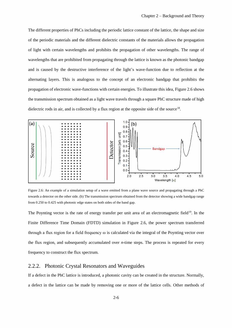
propagation of electronic wave-functions with certain energies. To illustrate this idea, Figure 2.6 shows
the transmission spectrum obtained as a light wave travels through a square PhC structure made of high
dielectric rods in air, and is collected by a flux region at the opposite side of the source18.
Figure 2.6: An example of a simulation setup of a wave emitted from a plane wave source and propagating through a PhC
towards a detector on the other side. (b) The transmission spectrum obtained from the detector showing a wide bandgap range
from 0.250 to 0.425 with photonic edge states on both sides of the band gap.
The Poynting vector is the rate of energy transfer per unit area of an electromagnetic field19. In the
Finite Difference Time Domain (FDTD) simulation in Figure 2.6, the power spectrum transferred
through a flux region for a field frequency ω is calculated via the integral of the Poynting vector over
the flux region, and subsequently accumulated over n-time steps. The process is repeated for every
frequency to construct the flux spectrum.
2.2.2. Photonic Crystal Resonators and Waveguides
If a defect in the PhC lattice is introduced, a photonic cavity can be created in the structure. Normally,
a defect in the lattice can be made by removing one or more of the lattice cells. Other methods of

Chapter 2 – Background and Theory
2-7
creating defects is by changing the size and/or the dielectric constant of one or more of the lattice cells.
In the example shown in Figure 2.7 (a), removing one of the rods creates a monopole defect cavity.
Introducing a defect can cause a localised state to form within the bandgap of the dispersion spectrum
of the crystal. This means when a light wave travels through the lattice, somewhere within the bandgap
transmission curve, a state can be found corresponding to the cavity mode, as illustrated in Figure 2.7
(b).
In the one-dimensional Bragg mirror approximation, a photonic cavity in a material with refractive
index, n (𝑛 = 1 in the illustration of Figure 2.7), has a mode when the cavity length 𝐿𝑐𝑎𝑣 is equal to an
integer multiple, 𝑚, of the intra-cavity half wavelength, λ, and is given by:
𝐿𝑐𝑎𝑣 =𝑚𝜆
2𝑛 (2.2)
The resonance occurs when there is a constructive interference caused by reflections of the wave due
to the photonic bandgap. This constructive interference produces a sharp cavity mode within the
bandgap region.
Figure 2.7: An example of a simulation setup of a wave emitted from a plane wave source and propagating through a PhC
structure towards a detector with a removed hole forming a cavity. (b) The transmission spectrum obtained from the detector
showing an opened cavity mode state within the band gap. The inset shows the Ey field profile of such a cavity.
The defect within a 2D PhC can be designed to confine a desired cavity mode wavelength within the
plane of the crystal. To confine the cavity mode in the third dimension, previous work has used total

Chapter 2 – Background and Theory
2-8
internal reflection rather than Bragg reflection. Krauss et al. were the first people to show
experimentally a 2D PhC cavity mode that harnesses total internal reflection for light confinement20.
The confinement strength of any cavity is determined primarily by the Q-factor of the cavity. The Q-
factor of a cavity is defined mainly by two parameters related to the cavity mode, these are the mode’s
frequency (or wavelength), 𝜔, and the lifetime of a photon confined inside the cavity, 𝜏. The lifetime
of a photon inside the cavity can be rationally thought of as the duration a photon can stay within the
cavity before it is scattered or absorbed. Ideal cavities have an infinite lifetime, i.e. the photons can be
trapped inside them without escaping. In practice however, the lifetime of a cavity is finite. The inverse
of the lifetime is the cavity decay rate, 𝜅:
𝜅 =1
𝜏𝑐𝑎𝑣 (2.3)
The Q-factor can then be defined as:
𝑄 =𝜔
𝜅 (2.4)
The most common PhC cavity design comprises one or more air-holes removed from a PhC hole lattice
fabricated on a high dielectric constant material such as GaAs or Si. The most common of these are the
H1 and the L3 cavities that are made of one and three removed holes, respectively. Scanning Electron
Microscopy (SEM) images of the H1 and L3 PhCs are shown in Figure 2.8. Another common cavity
design is based on the removal of one rod of a high dielectric constant periodic rod structure surrounded
by air. SEM images of such a structure is shown in Figure 2.9. The latter cavity design will be the main
type used in chapter 4, whilst the former will be mainly used in chapter 6.
The PhC cavities discussed before are defects within the photonic lattice and can be considered as a
localised disruption to the periodicity that act as optical resonators capable of confining electromagnetic
modes of discrete wavelengths located within the photonic bandgap wavelength range. A PhC
waveguide can be considered as a series of specially coupled point defects. Coupling between these
defects leads to the formation of a transmission band or guided mode in which the electromagnetic wave

Chapter 2 – Background and Theory
2-9
Figure 2.8: (a) An example of an H1 hole-type PhC cavity. (b) An example of an L3 hole-type PhC cavity. The two figures
show one and three removed holes of the lattice forming H1 and L3 cavities, respectively.
Figure 2.9: An example of a hexagonal lattice H1 rod-type PhC cavity, showing one missing rod from the hexagonal rods
lattice to form a rod-type photonic cavity.
is confined in all directions but is allowed to travel along the series of defects. In a similar fashion to
PhC cavities, PhC waveguides can utilise total internal reflection to confine light in the third dimension
whilst being confined due to the photonic bandgap in the other two dimensions.
A single mode waveguide can be created by removing a row of holes in a hole-type PhC, such that there
exists only one guided mode wavelength within the bandgap of the lattice. This makes PhC waveguides
very useful in light transfer on a photonic chip, beside its potential use in integrated wavelength filters

Chapter 2 – Background and Theory
2-10
due to its selectivity to couple to a discrete set of wavelengths21. A row of missing holes is called a W1
type waveguide and will be the main type considered in this thesis, see Figure 2.10.
Figure 2.10: SEM image of a typical W1 PhC waveguide designed for coupling to GaSb QDs with emission wavelengths of
~1250 nm. The waveguide is formed by creating a line defect in the lattice by simply omitting a line of holes to create a
propagating mode in the photonic bandgap system.
W1 waveguides are important since they can cause slow light effects22. Slow light is a term used to
describe light travelling through a medium with a group velocity that is much lower than the speed of
light in that medium. Slow light has many important applications in quantum information. This is
because by slowing light as it travels through a medium, stronger light-matter interactions can take
place, providing many opportunities for applications in optical buffering and quantum memories23,24. In
chapter 6, slow light is suggested to be used in phase modulators, hence shortening the needed
waveguide length for creating π-phase modulation compared to conventional phase modulators.
2.2.3. Purcell Enhancement
The advantage in using a photonic cavity system to couple to a single photon emitter such as a QD is to
increase the spontaneous emission rate of single photons from the QD25. This rate of single photon
emission is directly related to the bit rate achievable when the system is used in a QKD chip. By placing
a QD inside a photonic cavity, the electric field of the cavity mode can interact with the QD’s ground
and excited state. Chapter 3 will show how a cavity is fabricated around a QD for this type of experiment
to be carried out.
Chapter 2 – Background and Theory
2-11
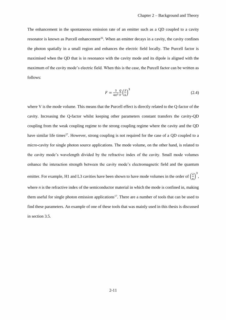
The enhancement in the spontaneous emission rate of an emitter such as a QD coupled to a cavity
resonator is known as Purcell enhancement26. When an emitter decays in a cavity, the cavity confines
the photon spatially in a small region and enhances the electric field locally. The Purcell factor is
maximised when the QD that is in resonance with the cavity mode and its dipole is aligned with the
maximum of the cavity mode’s electric field. When this is the case, the Purcell factor can be written as
follows:
𝐹 =3
4𝜋2
𝑄
𝑉(
𝜆
𝑛)
3 (2.4)
where V is the mode volume. This means that the Purcell effect is directly related to the Q-factor of the
cavity. Increasing the Q-factor whilst keeping other parameters constant transfers the cavity-QD
coupling from the weak coupling regime to the strong coupling regime where the cavity and the QD
have similar life times27. However, strong coupling is not required for the case of a QD coupled to a
micro-cavity for single photon source applications. The mode volume, on the other hand, is related to
the cavity mode’s wavelength divided by the refractive index of the cavity. Small mode volumes
enhance the interaction strength between the cavity mode’s electromagnetic field and the quantum
emitter. For example, H1 and L3 cavities have been shown to have mode volumes in the order of (𝜆
𝑛)
3,
where n is the refractive index of the semiconductor material in which the mode is confined in, making
them useful for single photon emission applications17. There are a number of tools that can be used to
find these parameters. An example of one of these tools that was mainly used in this thesis is discussed
in section 3.5.

Chapter 2 – Background and Theory
2-12
Single Photon Detectors
Single photon detectors (SPDs) are one of the main components that determine the speed and efficiency
of a QKD system28. An ideal SPD is expected to click every time it receives a photon, at an arbitrary
speed29,30. Practical SPDs that are incorporated in QKD systems are far from ideal. For example, the
quantum efficiency, which is the percentage of photons incident on the device’s photoreactive surface
and produce charge carriers, may be less than 100%. The dark count, which is the rate the detector
outputs pulses in the absence of any incident photon, and the dead time, which is the time in which a
detector is not capable of detecting a photon after a photon detection event, are both usually non-zero
in practice. The dead time also reduces the “photon number resolution”, which is the ability to
distinguish the number of photons in an incident pulse. The time jitter is also an important factor, it can
be defined as the time delay variations between the input of the optical signal and the output of the
electrical signal. This in practice may also be non-zero.
There are different physical methods that allow the realisation of SPD devices. The first uses
superconducting nanowires that are typically 5 nm thin, 100 nm in width and a few hundreds of microns
in length patterned in a grid like structure31-33. During operation, the wire is cooled below its
superconducting critical temperature and a DC bias current that is close to but less than its
superconducting critical current is applied. When a photon is absorbed by the nanowire grid, it breaks
electron Cooper pairs and reduces the local critical current below that of the bias current, causing an
increase in resistance at the region of the incident photon. This perturbation in resistance causes a
change in the bias current, typically measurable by sensitive electronic instruments. Superconducting
nanowire SPDs are known to have high quantum efficiency and relatively small dark counts, in
comparison to avalanche photodetectors (APDs) that will be described later. However, the limiting
factor that prevents this technology from being incorporated in commercial products in the future, is
their operation temperature which is typically required to be only a few degrees above absolute zero.
A more interesting technique in realising SPDs is by exploiting the avalanche effect when a P-I-N
junction is reverse biased. Such detector types have been implemented on Silicon and III-V materials.
Chapter 2 – Background and Theory
2-13
In the next section, a brief overview of P-I-N junctions together with the working principles of APDs
will be given as background material for chapter 5 which involves using nanowire P-I-N junctions for
photodetection.
2.3.1. P-I-N Junctions
In section 2.1.1, the basics of semiconductor materials were introduced. It was introduced that
semiconductors have been widely used in electronic devices due to the ability to engineer their
conductivity for different applications. Changing the conductivity can be done by doping the
semiconductors with atoms to introduce negative (n-doping) and positive (p-doping) charge carriers,
electrons and holes. In the n- and p-doped regions, the carrier concentrations are a few orders of
magnitude higher than the concentration of carriers in the intrinsic region. Sandwiching an intrinsic
semiconductor region between an n-doped and a p-doped region makes a p-i-n junction. This structure
has many applications in high power electronics and is suitable for fast switches, attenuators and
photodetectors. The latter is the main use for p-i-n junctions in this thesis. Between the p-i-n junction,
there exists a layer even larger than the intrinsic region, known as the depletion region. This is formed
by charge carriers combining and annihilating one another through diffusion from the p- and the n-
doped regions. This diffusion becomes limited by the electric field created by positive and negative ions
left behind in the n and p regions, respectively.
Under forward bias, the p-type region is connected to the positive terminal of a power source and the
n-type is connected to the negative terminal. Electrons and holes from the n-type and the p-type regions
are forced towards the intrinsic region due to the potential difference of the source. Some charge carriers
recombine at the intrinsic region and others continue to flow through the opposite side of the junction
creating an electric current.
When a p-i-n junction is reverse biased, the depletion region widens and ordinarily the junction does
not conduct, except for a small leakage current. If a photon of sufficient energy is absorbed by the
depletion region of the diode, the absorption process creates an electron-hole pair within the depletion

Chapter 2 – Background and Theory
2-14
region, as shown in Figure 2.11. The applied reverse bias field pulls the electrons and holes, out of the
region, toward the source’s terminal, causing a current flow34.
Figure 2.11: (Left) p-i-n junction under reverse bias, showing the regions of majority electron and hole carriers, an incident
photon on the intrinsic region and the created electron-hole pair. (Right) Band diagram for the corresponding p-i-n junction
with the created electron-hole pair due to an incident photon on the intrinsic region. The excited electron and hole carriers are
attracted toward the n and p-regions respectively due to reverse bias, causing a current spike which can be amplified and
measured by sensitive electronics.
2.3.2. Avalanche Multiplication
Avalanche multiplication is a phenomenon that can occur in semiconductor and insulating materials
where an electric current multiplication allows high currents to be generated in an otherwise insulating
materials27. In p-i-n junctions, the phenomena occurs when, following the absorption of a photon,
carriers are accelerated from the depletion region by the electric field of an applied reverse bias. If the
charge carriers have enough kinetic energy, collisions with other bound electrons can excite them across
the bandgap and create other free electron-hole pairs (secondary carriers). These secondary carriers
accelerate due to the applied bias and gain enough energy to create even more carriers in a cascaded
process. Hence a single photon can create a sudden increase in current at the junction. The current
created by the multiplicative process of carriers due to the absorption of a single photon makes
avalanche multiplication an ideal process for realising semiconductor SPDs.

Chapter 2 – Background and Theory
2-15
Differential Phase QKD Protocols
The QKD scheme described in chapter 1, encodes quantum information on photon polarisations using
two non-orthogonal bases. An alternative encoding approach uses the phase difference between
successive photon pulses interfering at a beam splitter at the end of a Mach-Zehnder interferometer.
This method of encoding information is known as Differential Phase Shift (DPS) QKD35.
One of the key components in a DPS-QKD systems is a Mach-Zehnder interferometer. To illustrate the
operation principles of DPS-QKD, it is important to explain how a Mach-Zehnder interferometer work
for large photon number pulses. In this type of interferometers, the input laser beam is split in a 50:50
beam splitter, resulting in two beams, one can be called the modulated beam (marked yellow) and the
other can be called the reference beam (marked red), as shown in Figure 2.12.
Figure 2.12: A block diagram of a typical DPS-QKD system with two pulses, coloured red and yellow, taking the different
path in the Mach-Zehnder interferometers. The laser is input from the bottom left as shown by the blue arrow and split by a
beam splitter. One arm contains a phase modulator which causes phase shifting one arm relative to the other. Constructive and
destructive phase shifting can be recorded by detectors 0 and 1 respectively.
Let’s define 𝑙1 and 𝑙2 as the total path length for the modulated and reference beams respectively. When
the light passes through a glass beam splitter it exhibits a phase shift equivalent to 2𝜋𝑡/𝜆, where 𝑡 is
the thickness of the beam splitter. For detector 0, the modulated beam takes a phase shift of 𝜋 from the
Chapter 2 – Background and Theory
2-16
first beam splitter, a 𝜋 phase shift from the top mirror, a 2𝜋𝑡/𝜆 from the last beam splitter, and the path
length of 2𝜋𝑙1/𝜆, before reaching detector 0 . This gives a total of
2𝜋 + 2𝜋 (𝑙1 + 𝑡
𝜆)
The reference beam takes a phase shift of 2𝜋𝑡/𝜆 as it goes through the first beam splitter, a 𝜋 phase
shift as it gets reflected by the bottom mirror and another 𝜋 phase shift as it gets reflected by the second
beam splitter toward detector 0. Hence the phase difference between the two beams 𝜙, which is caused
by the phase modulator is:
2𝜋 + 2𝜋 (𝑙1 + 𝑡
𝜆) − 2𝜋 − 2𝜋 (
𝑙2 + 𝑡
𝜆) = 𝜙
2𝜋 (𝑙1 − 𝑙2
𝜆) = 𝜙
In a similar fashion, the phase difference between the two arms for detector 1 is:
2𝜋 + 2𝜋 (𝑙1 + 2𝑡
𝜆) − 𝜋 − 2𝜋 (
𝑙2 + 2𝑡
𝜆) = 𝜙
𝜋 + 2𝜋 (𝑙1 − 𝑙2
𝜆) = 𝜋 + 𝜙
Hence, it is clear to note that when the phase modulator causes a zero phase shift, there is a constructive
interference on the path to detector 0, and a destructive interference to detector 1. By varying 𝜙, this
condition can be changed, hence changing the probability of arrival at either detector.
A simplified example of a DPS-QKD system is shown in Figure 2., where Alice generates a train of
single photon pulses and passes it through a Mach-Zehnder interferometer. In the interferometer, Alice
splits the signal through a beam splitter, and applies a random phase modulation of 0, π
2,
3π
2, or π on one
arm and recombines the two arms at the junction of a second beam splitter. She later sends the signal to
Bob through a quantum channel such as a fibre optic or free space. At Bob’s side, he performs a similar
Mach-Zehnder interferometry process, where he splits the signal into two arms, performs a random 0

Chapter 2 – Background and Theory
2-17
or π
2 phase-shift through one arm and recombines the two arms in a beam splitter. There are three
detection time slots at which Bob can measure. The first is when two consecutive pulses take the long
paths on Alice’s and Bob’s interferometers. The second is when the two pulses both take the short paths
of the interferometers. Both of these events aren’t of use in this protocol. The only used events are when
a pulse takes the long and short arm of Alice and Bob sides while the other takes the short and long
arms of Alice and Bob respectively, as shown in Figure 2.. If the interferometers on both sides are
matched, as when Alice and Bob use a similar basis, a 0 or π phase shift takes place between two
successive photon pulses, causing trigger events in either detector 0 or 1, as shown in Figure 2.. In a
real implementation, each single photon pulse is accompanied by one proceeding bright pulse for timing
purposes. The bright photon pulse will appear as two pulses on Bob’s detectors as it goes through the
two long and two short paths in Alice and Bob sides.
Figure 2.13: A block diagram of a typical DPS-QKD system with two pulses, coloured red and yellow, taking the different
path in the Mach-Zehnder interferometers.
After receiving the qubits, Bob announces publicly the time slots at which a photon was detected by
one of his detectors, but does not reveal which detector detected it. From Alice’s modulation data, she
can know which detector in Bob’s end recorded the event. By designating detection events recorded by
detector 0 and 1 as key bit values 0 and 1, respectively, they can share an identical bit string.
In an ideal system where there are no errors in the detection events, the sifted key created is
unconditionally secure. However, in practice, as discussed in chapter 1, all QKD systems have a
baseline error rate, hence error correction and privacy amplification procedures are essential in a
practical DPS-QKD system.

Chapter 2 – Background and Theory
2-18
Figure 2.14: An example of a click event observed on detector 0 due to a 0 degrees phase shift representing a 0 bit. This occurs
when two consecutive pulses take opposite and alternate arms on Alice and Bob’s ends. The figure also shows timing pulses
measured by the detector.
After error correction, when the error threshold is low enough to allow carrying on with the protocol,
to nullify any information that may have been obtained by an eavesdropper, Eve, privacy amplification
is performed36. This allows making Eve’s information of the final shared key extremely small. In
privacy amplification, Alice and Bob apply hash algorithms that uses the error free shared key as an
input and outputs a new shorter key.
Bright
timing
pulses

Chapter 2 – Background and Theory
2-19
Bibliography
1 D. A. Neamen. Semiconductor physics and devices, basic principles. Third edition. McGraw Hill,
ISBN 0-07-232107-5 (2003)
2 F. Bloch, Z. Physik. Uber die Quantenmechanik der Elektronen in Kristallgittern 52, 555-600 (1928)
3 R. Kronig, W. G. Penney. Quantum Mechanics of Electronics in crystal lattices. Proc. Roy. Soc.,
A130, 499-513 (1931)
4 P. Michler. Single quantum dots, fundamentals, applications and new concepts. Springer, ISBN 3-
540-140220-0 (2003)
5 N. Gisin, G. Ribordy, W. Tittel, H. Zbinden. Quantum Cryptography. Rev. Mod. Phys., 74, 145-195
(2002)
6 C. B. Murray, C. R. Kagan, M. G. Bawendi. Synthesis and characterization of monodisperse
nanocrystals and close-packed nanocrystal assemblies. Annual Review of Materials Research, 30 (1),
545-610 (2000)
7 Y. Makhlin, G. Schön, A. Shnirman. Quantum-state engineering with Josephson-junction devices.
Rev. Mod. Phys., 73, 357 (2001)
8 Z. M. Wang. Self-assembled quantum dots. Springer, ISBN 978-0-387-74190-1 (2008)
9 C. Chakraborty, L. Kinnischtzke, K. M. Goodfellow, R. Beams, A. N. Vamivakas. Voltage-controlled
quantum light from an atomically thin semiconductor. Nature Nanotechnol. 10, 507-512 (2015)
10 P. Frigeri, L. Seravalli, G. Trevisi, S. Franchi. Molecular beam epitaxy: an overview. Comprehensive
Semiconductor Science and Technology, 3, 480-522 (2011)
11 R. C. Jaeger. Introduction to microelectronic fabrication. Upper Saddle River: Prentice Hall, volume
5, ISBN 0-201-44494-1
12 I. N. Stranski, L. Krastanow. Zur Theorie der orientierten Ausscheidung von Ionenkristallen
aufeinander. Abhandlungen der Mathematisch-Naturwissenschaftlichen Klasse IIb. Akademie der
Wissenschaften Wien, 146, 797-810 (1938)
13 F. Hatami, N. N. Ledentsov, M. Grundmann, J. Böhrer, F. Heinrichsdorff, M. Beer, D. Bimberg, S.
S. Ruvimov, P. Werner, U. Gösele, J. Heydenreich, U. Richter, S. V. Ivanov, B. Y. Meltser, P. S.
Kop’ev, Zh. I. Alferov. Radiative recombination in type-II GaSb/GaAs quantum dots. Appl. Phys. Lett.,
67, 656-658 (1995)
14 J. Y. Marzin, J. M. GéRard, A. Izraél, D. Barrier, G. Bastard. Photoluminescence of single InAs
quantum dots obtained by self-organised growth on GaAs. Phys. Rev. Lett., 73, 716-719 (1994)
15 O. Briot, B. Maleyre, S. Ruffenach. Indium nitride quantum dots grown by metalorganic vapour phase
epitaxy. Appl. Phys. Lett., 83, 2919-2921 (2003)
16 Z. Lin, B. R. Carvalho, E. Kahn, R. Lv, R. Rao, H. Terrones, M. A. Pimenta, M. Terrones. Defect
engineering of two-dimensional transition metal dichalcogenides. IOP 2D Matter, 3, 022002 (2016)
Chapter 2 – Background and Theory
2-20
17 J. D. Joannopoulos, S. G. Johnson, J. N. Winn, R. D. Meade. Photonic crystals: modelling the flow
of light, Second edition. Princeton University Press, ISBN 978-0-691-12456-8 (2011)
18 S. G. Johnson, S. Fan, P. R. Villeneuve, J. D. Joannopoulos. Guided modes in photonic crystal slabs.
Phys. Rev. B: Condens. Matter. Phys., 60, 5751-5758 (1999)
19 J. A. Stratton. Electromagnetic theory (1st ed.). New York: McGraw-Hill. ISBN 978-0-470-13153-4
(1941)
20 T. F. Krauss, R. M. De La Rue, S. Brand. Two-dimensional photonic-bandgap structures operating
at near-infrared wavelengths. Nature, 383, 699-702 (1996)
21 Y. A. Vlasov, M. O’Boyle, H. F. Hamann, S. J. McNab. Active control of slow light on a chip with
photonic crystal waveguide. Nature, 438, 65-69 (2005)
22 T. Baba. Slow light in photonic crystals. Nature, 2, 465-473 (2008)
23 M. Notomi, K. Yamada, A. Shinya, J. Takahashi, C. Takahashi, I. Yokohama. Extremely large group-
velocity dispersion of line-defect waveguides in photonic crystal slabs. Phys. Rev. Lett., 87, 253902
(2001)
24 A. Javadi, I. Sollner, M. Arcari, S. Lindskov Hansen, L. Midolo, S. Mahmoodian, G. Kirsanske, T.
Pregnolato, E. H. Lee, J. D. Song, S. Stobbe, P. Lodahl. Single-photon non-linear optics with a quantum
dot in a waveguide. Nature Commun., 6, 8655 (2015)
25 P. Lodahl, S. Mahmoodian, S. Stobbe. Interfacing single photons and single quantum dots with
photonic nanostructures. Rev. Mod. Phys., 87, 347-400 (2015)
26 E. M. Purcell. Spontaneous emission probabilities at radio frequencies. Phys. Rev., 69, 674 (1946)
27 J. P. Reithmaier, G. Sek, A. Löffler, C. Hofmann, S. Kuhn, S. Reitzenstein, L. V. Keldysh, V. D.
Kulakovskii, T. L. Reinecke, A. Forchel. Strong coupling in a single quantum dot semiconductor
microcavity system. Nature, 432, 197-200 (2004)
28 V. Scarani, H. Bechmann-Pasquinucci, N. J. Cerf, M. Dusek, N. Lutkenhaus, M. Peev. The security
of practical key distribution. Rev. Mod. Phys., 81, 1301-1350 (2009)
29 M. D. Eisaman, J. Fan, A. Migdall, S. V. Polyakov. Invited review article: Single-photon sources and
detectors. Rev. Sci. Instrum., 82, 071101 (2011)
30 L. C. Comandar, B. Frohlich, M. Lucamarini, K. A. Patel, A. W. Sharpe, J. F. Dynes, Z. L. Yuan, R.
V. Penty, A. J. Shields. Room temperature single-photon detectors for high bit rate quantum key
distribution. Appl. Phys. Lett., 104, 021101 (2014)
31 Robert H Hadfield. Single-photon detectors for optical quantum information applications. Nature
Photon., 3, 696-705 (2009)
32 F. Marsili, V. B. Verma, J. A. Stern, S. Harrington, A. E. Lita, T. Gerrits, I. Vayshenker, B. Baek, M.
D. Shaw, R. P. Mirin, S. W. Nam. Detecting single infrared photons with 93% system efficiency. Nature
Photon., 7, 210-216 (2013)
33 C. M. Natarajan, M. G. Tanner, R. H. Hadfield. Superconducting nanowire single-photon detectors:
physics and applications. Supercond. Sci. Technol., 25, 063001 (2012)

Chapter 2 – Background and Theory
2-21
34 W. T. Tsang. Semiconductors and semimetals. Part D photodetectors. Academic Press, ISBN 978-0-
12-752153-4 (1985)
35 K. Inoue, E. Waks, Y. Yamamoto. Differential Phase shift quantum key distribution. Phys. Rev. Lett.,
89, 037902 (2002)
36 C. H. Bennett, G. Brassard, C. Crepeau, U. Maurer. Generalized privacy amplification. IEEE Trans.
Inf. Theory, 41, 1915 (1995).
Chapter 3 – Device Fabrication and Experimental Techniques
3-1
Chapter 3
Device Fabrication and Experimental
Techniques
Introduction
Many tools and experimental techniques were used for designing, simulating, growing, fabricating and
testing the devices discussed in this thesis. Designing and simulating the photonic components for
quantum key distribution (QKD) were done using MIT’s Electromagnetic Equation Propagation
(MEEP), which is a Finite Difference Time Domain (FDTD) tool written by Oskooi et al1. Growth of
the quantum dots (QDs) and nanowires was done using molecular beam epitaxy (MBE). Fabrication of
the devices was achieved using electron-beam (e-beam) lithography, thermal evaporation and
inductively-coupled plasma reactive ion etching (ICP-RIE). Fabrication inspections of the devices were
done using atomic force microscopy (AFM) and scanning electron microscopy (SEM). Micro-
photoluminescence spectroscopy was carried out using an in-house built setup to perform optical
characterisation of the devices. In this chapter of the thesis, a summary of these tools and techniques
will be given. The following sections will summarise and discuss the fabrication recipes and the
challenges faced to realise the hole-type photonic crystals (PhCs).
Some of the novel aspects in this chapter involve the use of CSAR62, a resist used as an alternative to
PMMA for e-beam lithography. A comparison will be made between using CSAR62 and PMMA as
etching masks in ICP-RIE dry etching. Selectivity results with etching GaAs using chlorine based gases
Chapter 3 – Device Fabrication and Experimental Techniques
3-2
will be given. Other novelties in this chapter include performing high temperature dry etching to achieve
high aspect ratios in etching hole-type PhCs. A comparison will be made between the achievable etching
profiles as the table temperature of the ICP-RIE is increased.
Fabrication Techniques
3.2.1. Electron-Beam Lithography
Semiconductor device fabrication involves many processes and techniques used to create integrated
electronic and photonic circuits for use in a wide range of applications. Device fabrication usually
involves a series of steps such as lithography, chemical processing and physical etching etc. before
achieving the final desired structure on a semiconductor material.
In nanofabrication, lithography is a technique used in patterning an integrated circuit structure on a thin
film, such as a resist, or the bulk substrate. The most common type of lithography techniques are
photolithography2 and e-beam (e-beam)3 lithography. There are other methods for performing
lithography such as nanoimprint lithography4, interference lithography5, X-ray lithography6, magneto
lithography7 and scanning probe lithography8. The photonic structures investigated in this thesis
requires nanometre resolution lithography techniques. This high-resolution requirement is particularly
important in fabricating PhCs operating in the visible/near-infrared wavelength range. The challenge in
fabricating PhCs lies in their requirement to be precisely fabricated as needed in the design and
simulation process to ensure they keep their optical properties and prevent photonic losses. This makes
e-beam lithography that typically has sub-nanometre resolution, the ideal tool for fabricating PhCs. The
disadvantage of using e-beam lithography is its slow throughput speed, where multiple devices can only
be written in a serial manner. For this reason, it is not generally suitable for the mass manufacturing of
devices as the processing time scales linearly with the number of devices being produced, whilst other
parallel techniques can scale sub-linearly. A potential technique that can be utilised in the future for
PhC fabrication is nanoimprint lithography, which can achieve a resolution lower than 10 nm, thus
suitable enough for visible wavelengths PhCs. Previous reports have shown PhC structures fabricated

Chapter 3 – Device Fabrication and Experimental Techniques
3-3
with scanning probe lithography. Since most of the devices presented in this thesis are fabricated with
e-beam lithography, the focus of this section will be on introducing e-beam lithography.
E-beam lithography is the process of using a beam of electrons to write a pattern on an e-beam sensitive
resist. The resist layer is normally span coated on a substrate, and by exposing and scanning the resist
with an e-beam, using an e-beam writer, the desired pattern can be achieved. Long molecular chains
that the resist consists of break after the application of the e-beam making the exposed areas on the
resist dissolvable in a suitable chemical solution. The high achievable resolution with e-beam
lithography is due to the sub-nanometre size de Broglie wavelength of electrons, which is much shorter
than UV light wavelengths, that is typically used in photolithography. The e-beam writer used in
fabricating the devices presented in this thesis is a JEOL-JBX-5500ZD. A schematic illustration of a
typical e-beam writer is shown in Figure 3.1.
Figure 3.1: A simplified schematic illustration of a typical e-beam writer, similar to that of a scanning electron microscope.
The figure shows the e-beam path as it travels through the anode, magnetic lens, scanning coils before exposing the sample.
Secondary electrons emitted by the sample and backscattered electron are detected by different detectors for imaging and
calibration.

Chapter 3 – Device Fabrication and Experimental Techniques
3-4
In the JEOL system, an e-beam is generated from a cold field emission electron gun, and the e-beam is
attracted by an anode that is normally at a potential of 50 kV. The gun is made of a crystalline tungsten
tip that is very sharp, typically less than 0.1 μm at its end, hence creating a strong electric field at the
tip. The beam is then passed through a series of electromagnetic condensing lenses that reduce the
diameter of the beam. The beam is then passed through a beam limiting aperture, where the aperture
size used in the JEOL system is normally 40μm. Finally, the beam diameter is focused on the sample
by an objective lens where the diameter size of the beam typically reaches < 1 𝑛𝑚. During the writing
and alignment process, the scanning coils are used to scan the beam on the sample and pattern the
desired structure. The backscattered and secondary electrons detectors are used to image the surface by
detecting electrons scattered and those emitted by the sample, respectively.
The system is typically operated under high vacuum to prevent electron scattering and losses as they
travel through the column. Unless stated otherwise, most devices are patterned using a 50 pA beam
current, however the base dosage together with the modulation were altered. The high acceleration
voltage of the system provides the necessary resolution for fabricating nanostructures. This is due to
the reduced angle of backscattering, as shown in Figure 3.2. For PhC devices that have dense structures
and require precise writing patterns, a dosage modulation tool, known as Beamer, is utilised to reduce
shape changes in the written pattern due to forward and backscattered electrons. This is also known as
Proximity Effect Correction (PEC).
In forward scattering, an accelerated electron from the beam collides with another electron from one of
the atoms within the substrate/resist. The incident electron will change its direction of travel while
transferring parts of its energy to the atom which becomes ionised, creating a secondary electron. In
backscattering, an electron collides with a much heavier nucleus from a resist/substrate, causing it to
elastically scatter. The scattering angle due to backscattering is usually much larger than that for forward
scattering. Some electrons return back through the resist at a significant distance from the incident beam
point. This causes enlargement in the exposed regions of the resist as shown in Figure 3.3 (a and b).
Hence, PECs are utilised to reduce the enlargement caused by backscattered electrons.

Chapter 3 – Device Fabrication and Experimental Techniques
3-5
Figure 3.2: A schematic illustration showing a comparison between the spread of a beam accelerated by a 20kV and a 50kV
acceleration voltage as it penetrates through a substrate. Electrons with higher accelerating voltages can penetrate to greater
depths due to their high velocity, reducing backscattering angles.
In brief, there are mainly two methods to perform PEC, the first is shape modification and the second
is dosage modification. Performing the PEC correction often needs the accelerating voltage of the used
e-beam writer and the materials of the substrate, resist and developer as inputs. In shape modification,
a single dosage is used for the entire structure. The software uses an algorithm to modify the patterned
structures whilst taking into account the base dosage applied and other variables to achieve a closer
approximation to the desired structure, Figure 3.3 (c and d). In dose modification, the pattern is divided
into segments or pixels and the software uses an algorithm to calculate the dosage needed for every
pixel in the mask, while taking into account the dosage applied to nearby pixels. This can be done by
calculating the convolution of multiple Gaussian functions from exposing every pixel. The disadvantage
of the dose modification method is that it may require large computation times for very large circuits
drawn with high-resolution. In addition, this technique requires advanced electronics to control the
applied dosage in the EBL system to account for the multi-dosage layers that the mask typically
composes of. However, compared to the shape modification method, closer matching between the
desired and the fabricated structures can be made using the dosage modification technique. On the other
hand, the disadvantage of the shape modification method is its incompetence in handling masks that

Chapter 3 – Device Fabrication and Experimental Techniques
3-6
involve large and small structures close to each other, since modification of the shape may lead to an
overlap between the different structures. A hybrid method of dosage and shape modification can also
be used for PECs. For example, to fabricate the desired structure shown in Figure 3.3 (e), the exposed
area is reduced and the structures is divided into regions of different dosage levels. Dividing the
structures into many dosage levels (typically tens to a few hundreds) with small increments between
each level allows realising the desired structure with good geometrical accuracy, as shown in Figure
3.3 (f). Considering the rectangle shown in Figure 3.3 it is important to notice that the rectangle is
exposed with low dosages near the centre, the dosage is increased though toward the edges of the
rectangle. This is because the average dosage per area accumulated near the centre will be higher
compared to those near the edges when a single dosage was used for the whole rectangle.
Figure 3.3: An illustrative diagram of proximity effects on the achieved pattern. (a and b) An illustration of the enlargement
occurs as the pattern is exposed with one constant dosage. (c and d) The enhancement obtained in the developed shape size,
as the shape of the exposed region is changed. (e and f) Even better enhancement obtained as the pattern is shrunk and divided
into regions of different dosages, where outer regions are exposed to higher dosage compared to inner regions, hence
maintaining the same average dosage throughout the pattern.

Chapter 3 – Device Fabrication and Experimental Techniques
3-7
3.2.2. Thermal (Resistive) Evaporation
Resistive evaporation9 is a popular technique in the semiconductor microfabrication industry used to
accurately deposit nanoscale films of metals or other materials on a substrate. The metal is either
evaporated by applying an electric current through a filament crucible or sublimated off a tungsten wire.
A schematic of a resistive evaporator system is shown in Figure 3.4. This method should not be confused
with Molecular Beam Epitaxy which can also be classified as a form of thermal evaporation, MBE
systems are not included in this discussion (see section 3.2.4).
Inside the chamber, an oscillating crystal is fitted to measure the deposition rate, which can be used to
calculate the achieved thickness10. The working principle behind the oscillator is that the oscillation
frequency is changed as the mass of the oscillator is increased when the material is deposited on it. An
electronic instrument continuously reads the resonance frequency of the oscillator and applies
appropriate algorithms to convert the frequency data to deposition rates in real time.
There are many other methods that can be used for thin film metal deposition such as e-beam
evaporation and plasma sputtering9. The advantage that resistive evaporation has over other methods is
its simplicity, cheap system maintenance and compatibility with most metals. Thermal evaporation of
Chromium for its use as a hard etching mask in fabricating the rod-type PhC is discussed in chapter 4.
3.2.3. Lift-Off
Lift-off is a process used widely in the microfabrication industry for transferring a pattern of a specific
material, usually metals, on a substrate using a sacrificial material, such as a resist11. The desired pattern
is first patterned on a sacrificial layer, where areas of the sacrificial layer are removed exposing the
underlying substrate to be deposited on, see Figure 3.5 (a). A metal layer is then deposited to cover the
exposed regions of the substrate and cover remaining regions of the sacrificial layer, as shown in Figure
3.5 (b). The lift-off process involves inserting the whole substrate in a solution that dissolves the
sacrificial layer and removes it together with the capping metal layer, as shown in Figure 3.5 (c and d).
It is necessary that the lift-off solvent used is not reactive with the metal deposited but only dissolves
the sacrificial layer material.

Chapter 3 – Device Fabrication and Experimental Techniques
3-8
Figure 3.4: A schematic illustration of a thermal evaporator system. The chromium is coated around a tungsten filament and
is sublimated when a current is applied across the tungsten filament. Heating of the tungsten filament is made by a variable
current source. The deposition rate is measured by a crystal oscillator connected to an amplifier and calibration electronics.
Figure 3.5: A schematic illustration of the lift off process. (a) First the inverse pattern is transferred on the substrate using a
resist (b) A metal (such as Chromium) is deposited, covering the exposed regions of the substrate and the regions capped with
a resist. (b) The whole sample is placed in lift-off solvent such as acetone, which dissolves the resist and removes the metal
layer on top of them, leaving only regions where the metal is stuck to the substrate unaffected.

Chapter 3 – Device Fabrication and Experimental Techniques
3-9
It will be shown later in chapter 4 that a lift-off process is used in fabricating rod-type PhCs utilising
hard metal mask to provides better etching selectivity.
3.2.4. Molecular Beam Epitaxy
Molecular beam epitaxy (MBE) is a common technique for thin film deposition of materials such as
metals and semiconductors12. The word epitaxy originates from ancient Greek, where epi means
“above” and taxis means “ordered” or “arranged”. Hence, the word epitaxy can be translated as
“arranging upon” or “ordered above”. Compared to Chemical Vapour Deposition (CVD)13, MBE
systems do not use organic chemical precursors which normally increase background levels of
deposited carbon. In addition, the ultra-high vacuum that MBE operates at allows reducing other
environmental impurities within the chamber. Furthermore, MBE can provide very accurate
composition of the monolayer deposition and doping control. However, the complexity, price and
maintenance costs of MBEs make them less favourable for industrial processing in comparison to CVD
methods. In an MBE system, elements such as Gallium and Arsenic are heated in effusion cells to
evaporation temperatures and are allowed to condense on the wafer. Computerised shutters are placed
between the effusion cells and the wafer holder to allow precise control of the thickness of the deposited
material. The temperatures of the effusion cells are accurately controlled to regulate the deposition rate.
On the other hand, controlling the wafer’s temperature allows controlling the rate of hopping or
desorption of the deposited material14. To monitor the growth of the crystal layers on the wafer,
reflection high energy electron diffraction (RHEED) is used. Growing the GaSb QDs and the different
nanowires discussed in chapter 5 was carried out using a VG V80h MBE system.
3.2.5. Etching
Plasma dry etching is an essential tool used in the semiconductor fabrication industry. Plasma dry
etching together with wet etching were heavily used in fabricating most of the devices in this thesis. In
this section, a brief introduction to the concept of etching will be made together with overviews of dry
and wet etching15. In the section that follows, two very common techniques for dry etching will be
explained, these are Reactive Ion Etching (RIE)16 and Inductively Coupled Plasma (ICP)17.

Chapter 3 – Device Fabrication and Experimental Techniques
3-10
In micro and nano-fabrication, etching is the process of removing layers of a wafer to achieve a certain
structure. Before carrying out the etching process, some regions of the wafer are usually covered with
a mask to protect the underlying substrate against etching, whilst the uncovered areas are exposed to
the etchant material and etched away. The mask is usually defined by a lithography process; where the
mask may be the resist used in the lithography. There are two types of etching employed in the
semiconductor industry, these are wet and dry etching.
In wet etching, liquid chemical etchants are used to remove material from a wafer. The liquid is chosen
so that it reacts with the substrate and create other products that are usually dissolved and carried away
by the etchant solution. The substrate is normally rinsed in a different solution to stop the chemical
reaction by diluting any remaining etchant, and removing any by-products created as a result of the
reaction. The advantage that wet etching has is that it is simple and the etchants needed are normally
cheap. However, achieving anisotropic etching profiles with wet etching is usually to do. This makes
wet etching unsuitable in fabricating structures that need high etching verticality, as is the case for PhCs.
In chapter 5, hydrofluoric acid wet etching will be used to etch SiO2 for creating the nanowire sites for
their deterministic growth. Wet etching will also be used for releasing the suspended PhC bridge
structures in chapter 6.
In dry etching, a plasma is utilised together with etchant gasses to remove unmasked areas of a substrate.
There are two primary mechanisms that take place when dry etching a substrate, the first is chemical
etching and the second is physical etching (sometimes known as mechanical etching). While this may
sound simplistic, careful examination of the used recipe in dry etching to select between these two types
of etching mechanisms is necessary for optimised control over the etch. This is especially important in
etching fine features such as those in PhCs. In chemical etching, etchant gases react with the substrate
causing other materials to form. The by-products that result from the chemical etching process are
removed by the vacuum pump. In physical dry etching, high kinetic energy ions, electrons or photons
are used to etch the substrate. The high-energy particles bombard the substrate causing top-down

Chapter 3 – Device Fabrication and Experimental Techniques
3-11
sputtering of the atomic layers from the substrate. In chapter 4, dry etching will be used to create the
rods for the rod-type PhCs and will be used later in chapter 6 to etch the holes in the hole-type PhCs.
To create and sustain the plasma required for dry etching, energy is supplied by coupling an external
electric field and/or magnetic field to ionise the etchant gas and supply the ions with enough kinetic
energy to perform the etching. In the following sections, it will be shown that the different methods of
coupling the gases to different energy sources can provide control over the plasma. Compared to wet
etching, dry etching can provide a good control over the etch profile by adjusting parameters such as
the chamber pressure, the etchant gases’ flow rates, the etching time and the applied energy that ionises
and drives the ionised gas.
3.2.6. RIE and RIE-ICP
RIE is a technology utilised in the semiconductor micro-fabrication industry for dry etching15-17. RIE
uses a plasma to remove materials from a wafer substrate by chemical and physical means under low
pressures. Compared to RIE-ICP, RIE typically uses a parallel plate capacitor configuration (the
configuration is sometimes known as Capacitively Coupled plasma) to create an external electric field
for creating and sustaining the plasma inside the chamber. The wafer is normally situated in the bottom
of the chamber facing the plasma as shown in
. The RIE system used in this work is an Oxford Instrument Plasma Pro NGP80 supplied with Ar, O2,
SF6, CHF4 gases.
The electric field is applied between the capacitor plates using an RF generator operating at an industrial
frequency of 13.56 MHz, where the source power can range from a few watts to several hundred watts.
The oscillating electric field from the capacitor plates ionises the gas molecules by knocking out their
electrons. These electrons are accelerated within the oscillating plates knocking out other electrons to
further ionise the gas atoms, where those oscillate hitting the chamber walls and the lower electrode.
The chamber walls are grounded, hence electrons hitting the walls are removed. However, the
accumulation of electron charge on the bottom electrode builds up a potential difference that can be
measured by voltage measuring instruments. The potential difference between the lower electrode and
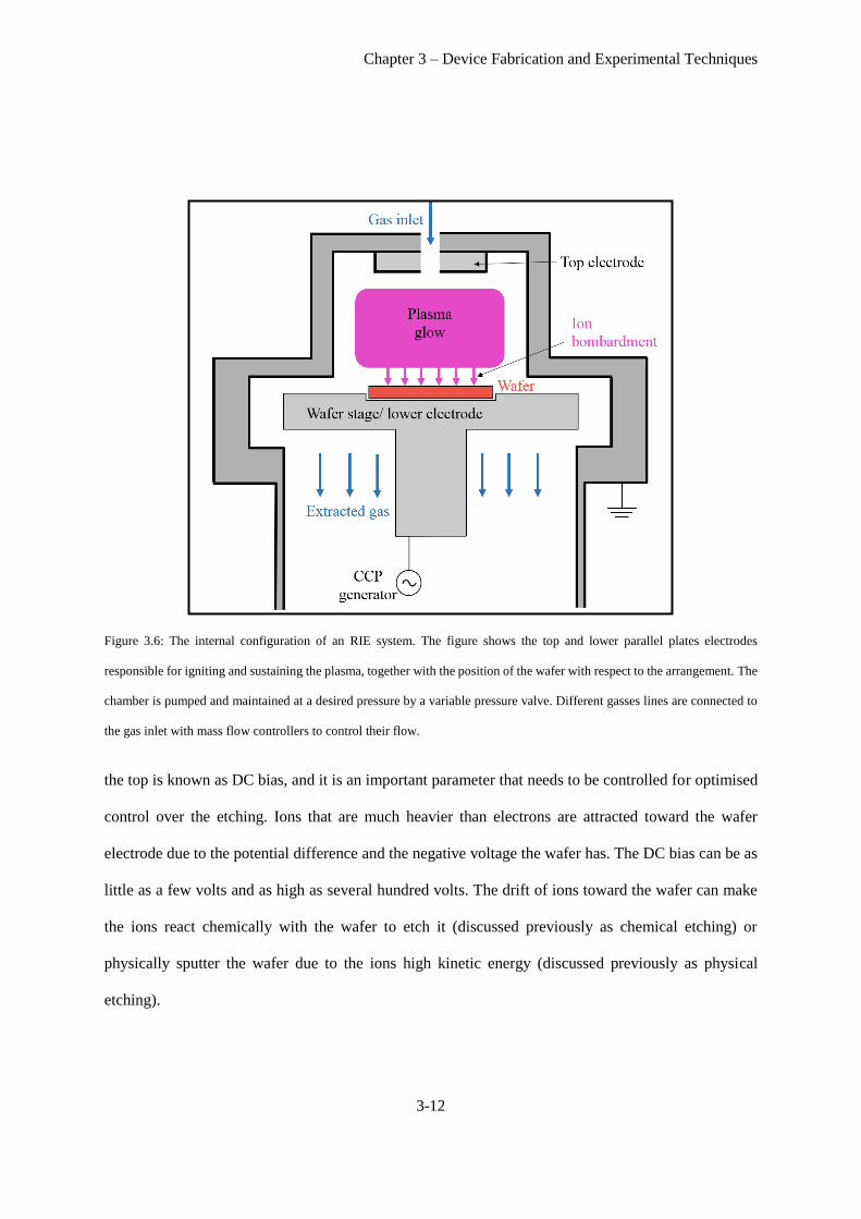
Chapter 3 – Device Fabrication and Experimental Techniques
3-12
Figure 3.6: The internal configuration of an RIE system. The figure shows the top and lower parallel plates electrodes
responsible for igniting and sustaining the plasma, together with the position of the wafer with respect to the arrangement. The
chamber is pumped and maintained at a desired pressure by a variable pressure valve. Different gasses lines are connected to
the gas inlet with mass flow controllers to control their flow.
the top is known as DC bias, and it is an important parameter that needs to be controlled for optimised
control over the etching. Ions that are much heavier than electrons are attracted toward the wafer
electrode due to the potential difference and the negative voltage the wafer has. The DC bias can be as
little as a few volts and as high as several hundred volts. The drift of ions toward the wafer can make
the ions react chemically with the wafer to etch it (discussed previously as chemical etching) or
physically sputter the wafer due to the ions high kinetic energy (discussed previously as physical
etching).

Chapter 3 – Device Fabrication and Experimental Techniques
3-13
An ICP-RIE system is similar in structure to an RIE system except for the addition of an N-turn
magnetic coil around the plasma discharge region. The inductor is connected to an RF generator and
delivers the energy to the gas via a time varying magnetic field inside the chamber. A simplified ICP-
RIE configuration is shown in Figure 3.7. The separate control over the inductively and capacitively
supplied energies to the plasma allows one to control the plasma density and other plasma parameters
without significantly changing the energy of the ions that bombard the sample. In other words, the ICP
can control the number of ions reaching the substrate for chemical etching while the CCP can control
the momentum of the ions that bombard the substrate. The ICP-RIE system used in this work is an
Oxford Instruments Plasmalab System 100 supplied with N2, H2, BCl3, Cl2, Ar, SF6, O2 gases. In the
following sections, discussions and analysis will be made of the effect of changing the etching
parameters on the achieved etching results.
Figure 3.7: A schematic illustration of an ICP-RIE system, showing the addition of the ICP coils in comparison with the RIE
system shown in
, which allows controlling the plasma density within the chamber and the chemical reaction.

Chapter 3 – Device Fabrication and Experimental Techniques
3-14
Scanning Probe Microscopy
Most of the fabricated features in this thesis required e-beam lithography due to the high resolution that
it provides compared to photolithography. Normally, visual and topological investigation of the
resultant developed patterns on an e-beam resist is essential to assist with identifying any source of
fabrication issues. This was especially important with using PMMA in fabricating the hole-type PhCs,
due to incomplete developing of the small and dense patterns that were exposed with fairly low dosages.
Using SEM for this purpose will expose the e-beam sensitive resist and cause further exposure to the
resist. This makes any further development to the pattern, if necessary, useless. Further exposure to
electrons may also cause cross linking in the resist, making it harder to strip off in later stages of the
device fabrication. For this reason, scanning probe microscopy (SPM) was frequently utilised in this
work to characterise the topographic structure of the resist after exposure.
SPM is a large branch of microscopy that utilises sharp probes to investigate a sample’s topological,
mechanical and electrical characteristics. A simplified illustrative figure for a scanning probe
microscope is shown in Figure 3.8. A sharp probe is mounted on a cantilever and allowed to contact the
sample by mounting the sample on an x-y-z piezo stage and moving it upwards until contact between
the tip and the sample is achieved. An applied external voltage across the piezo stage allows the sample
to be scanned beneath the probe to investigate the sample’s surface. A laser is calibrated to reflect from
the cantilever toward the centre of a four-quadrant photodiode. When the surface of a sample is scanned,
the probe is deflected based on the topography of the sample, causing the reflected laser spot to shift
from the centre of the photodiode. This shift is registered with time and a correlation between the
topography and probe position is recorded to output a topography map. The probe used in this work is
an Al coated Si tip with a pyramid height ranging from 4-6 μm, whilst the tip’s diameter is 12 ± 4 nm.
This aspect ratio is usually sufficient enough to allow the probe to reach the bottom of a fabricated PhC
hole with a radii of 55 nm and a depth of 120 nm. The AFM systems used in this work was either a
Veeco model NanoMan VS or a Veeco AFM CP-II.

Chapter 3 – Device Fabrication and Experimental Techniques
3-15
Figure 3.8: A simplified schematic diagram of the working principle of a scanning probe microscope. When the tip is scanned
laterally across the sample’s surface, deflections in the cantilever caused by the sample’s topology are measured by a quadrant
photodetector. The sample is mounted on a piezoelectrically driven stage to allow it to move during the scan process.
There were two imaging modes used to inspect the fabrication of the devices discussed in this thesis,
namely contact and tapping modes. In the contact mode, the tip approaches the sample and makes
contact throughout the whole scanning process. As the sample is moved during the scanning process,
the signal recorded at the photodetector is transferred to the control electronics where a feedback loop
allows the height of the sample to change in order to keep the force on the cantilever constant. The
change in the sample stage’s height is recorded to output the sample’s topography. The tapping method,
on the other hand, operates in a different way. In this method, the cantilever is oscillated at the cantilever
mechanical resonance frequency. Hence, the tip makes contact with the sample for very short periods
of time that depend on the resonance frequency, this is in contrast to the contact mode where the tip is
constantly in contact with the sample. In tapping mode, when the topography underneath the oscillating
tip is changed, the tip oscillation amplitude changes, hence the sample-tip separation is varied using a
feedback loop to maintain a constant oscillation amplitude of the tip. The topography map is then
inferred from sample-tip separation. Tapping mode was found to produce better images when small
features such as the PhC holes from Figure 3.11 are imaged. It was found that using contact mode, the

Chapter 3 – Device Fabrication and Experimental Techniques
3-16
tip struggles to reach the bottom of the exposed holes due to the low aspect ratio of the pyramidal shaped
tips.
Fabrication of Hole-Type Photonic Crystals
In this section, the fabrication methods and the challenges faced in fabricating the hole-type PhC
cavities discussed in chapter 6 will be explained. This includes the problems faced with developing
PMMA and the methods in which they were solved using CSAR62. A summary of the best dry etching
recipes that give the most anisotropic sidewalls for the holes will be given together with the effect of
different parameters that affect the etching profile. The steps for fabricating the structure are
summarised in Figure 3.9.
Initial attempts at fabricating the PhC were done using PMMA as an e-beam resist18. The sample was
spin-coated with a 200 nm PMMA layer and baked at 180 °C. Following this, the samples are patterned
with a 50 pA e-beam at 240 μC/cm2, which was found to be about the average dosage needed for PMMA
on a GaAs substrate using a 50kV writer. Using a different substrate such as Si, the dosage is usually
increased to account for the lower backscattering of electrons from the lighter atoms of Si compared to
GaAs. During the development process, two different solutions were used in removing the exposed
regions of the sample, these were Isopropanol (IPA):Deionized water (DI) 7:3 and Methyl Isobutyl
Ketone (MIBK):IPA 1:3. Both water and IPA are non-solvents for PMMA at room temperature. In
comparison to highly polar and the heavy molecular weight of MIBK, the less polar and lighter
IPA/water mixture can provide much better sensitivity because it can disintegrate and washoff the small
fractions of molecules that have been exposed by the e-beam.
However, there were two main issues faced when using PMMA as an e-beam resist for fabricating the
holes. In all fabrication attempts it was found that the PMMA resist was not developed deep enough to
the point where the underlying substrate was exposed. This was still the issue even when either of the
two developers (IPA:DI and MIBK:IPA) were used for long developing time periods. The developing
depth of the PMMA layer could have only been increased when the dosage was increased. However,

Chapter 3 – Device Fabrication and Experimental Techniques
3-17
for the purpose of fabricating the PhC this had the effect of increasing the holes’ radii due to increased
backscattering of electrons from the substrate, which is expected to reduce the cavities Q-factor and
change their resonance wavelength.
An alternative resist that was used to replace PMMA is CSAR6219. Similar to PMMA, this is a positive
e-beam resist that provides very high sensitivity and good contrast that is suitable for fabricating features
that require sub 10 nm resolution. The advantage that the cheap CSAR62 provides over PMMA is its
higher selectivity in dry etching, making it a strong competitor of ZEP520. The increased selectivity in
etching CSAR62 with GaAs makes the needed resist thickness that is required to mask the substrate
much smaller. This allows making holes with radii closer to those desired, which is aided by the thinner
resist typically having less faceting after development. In addition, due to the higher sensitivity of
CSAR62 compared to PMMA, a much smaller dosage is required to expose the pattern needed, this
reduces the increase that is expected to happen to the rod’s radii due to backscattering effects.
Figure 3.9: A schematic illustration showing for the steps of fabricating the hole-type PhC. (a) The resist is spun on the substrate
before the pattern was written with an e-beam writer and developed as shown in (b). (c) ICP-RIE dry etching is performed to
pattern the hole structure on the top GaAs layer. (d) Wet etching with HF is used to suspend the PhC structure by removing the
underlying AlGaAs layer.
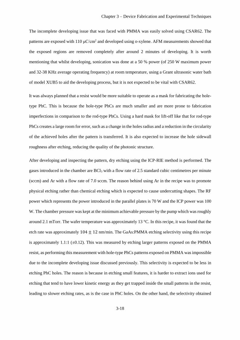
Chapter 3 – Device Fabrication and Experimental Techniques
3-18
The incomplete developing issue that was faced with PMMA was easily solved using CSAR62. The
patterns are exposed with 110 μC/cm2 and developed using o-xylene. AFM measurements showed that
the exposed regions are removed completely after around 2 minutes of developing. It is worth
mentioning that whilst developing, sonication was done at a 50 % power (of 250 W maximum power
and 32-38 KHz average operating frequency) at room temperature, using a Grant ultrasonic water bath
of model XUB5 to aid the developing process, but it is not expected to be vital with CSAR62.
It was always planned that a resist would be more suitable to operate as a mask for fabricating the hole-
type PhC. This is because the hole-type PhCs are much smaller and are more prone to fabrication
imperfections in comparison to the rod-type PhCs. Using a hard mask for lift-off like that for rod-type
PhCs creates a large room for error, such as a change in the holes radius and a reduction in the circularity
of the achieved holes after the pattern is transferred. It is also expected to increase the hole sidewall
roughness after etching, reducing the quality of the photonic structure.
After developing and inspecting the pattern, dry etching using the ICP-RIE method is performed. The
gases introduced in the chamber are BCl3 with a flow rate of 2.5 standard cubic centimetres per minute
(sccm) and Ar with a flow rate of 7.0 sccm. The reason behind using Ar in the recipe was to promote
physical etching rather than chemical etching which is expected to cause undercutting shapes. The RF
power which represents the power introduced in the parallel plates is 70 W and the ICP power was 100
W. The chamber pressure was kept at the minimum achievable pressure by the pump which was roughly
around 2.1 mTorr. The wafer temperature was approximately 13 °C. In this recipe, it was found that the
etch rate was approximately 104 ± 12 nm/min. The GaAs:PMMA etching selectivity using this recipe
is approximately 1.1:1 (±0.12). This was measured by etching larger patterns exposed on the PMMA
resist, as performing this measurement with hole-type PhCs patterns exposed on PMMA was impossible
due to the incomplete developing issue discussed previously. This selectivity is expected to be less in
etching PhC holes. The reason is because in etching small features, it is harder to extract ions used for
etching that tend to have lower kinetic energy as they get trapped inside the small patterns in the resist,
leading to slower etching rates, as is the case in PhC holes. On the other hand, the selectivity obtained

Chapter 3 – Device Fabrication and Experimental Techniques
3-19
in etching GaAs:CSAR62 was 1.9:1 (± 0.12). This greatly reduces the required thickness needed for the
resist to etch the holes completely through the GaAs layer until the AlGaAs layer is reached.
At this point, the current problem with fabricating the PhC was the large faceting obtained in the
sidewall profiles of the etched holes as shown in Figure 3.10 (a and b). The faceting can also be observed
from the top view image of the holes which show the dim surface inside the holes that are cause by
reflections of the electrons from the facets. The second problem which needed to be addressed was the
relatively slow etch rate obtained for etching the holes compared to etching larger features such as the
out-couplers. To solve these problems, the table temperature, and hence the wafer’s temperature, was
increased from 13 °C to 50 °C, whilst keeping the other etching parameters unchanged. This made the
etch rate of the holes comparable to that of the large features such as the out-coupler rings, while the
sidewalls profile shows better verticality. Both changes are attributed to an increase in the chemical
etching rate which sped up the etching process and helped undercutting the sidewalls, hence reducing
the facets. It was important to continue reducing the facets further to achieve holes with vertical
sidewalls. This was done by further increasing the table temperature to 100 °C while keeping other
etching parameters the same; the fabricated holes are shown in Figure 3.11. Clearly, from the top view
image of the holes there is a great reduction in the facets, identified by the sharply shaped circles in
comparison with those from Figure 3.10. The tilted image can also show the shadow of the side wall
profiles of the holes closest to the out-coupler rings. However, it is expected that this recipe cannot be
used for etching much deeper holes while maintaining the sidewalls vertical profile. This is because the
higher temperature provided an increased chemical etching rate in comparison with physical etching,
thus increasing the etching time for deeper sidewalls will likely form bow shapes due to increased
undercutting which is normally associated with chemical etching.
Beside the improvement in the etch rate of small features and the enhanced anisotropy in the etching
profile, etching at higher temperatures was found to improve the etching selectivity. At 100 °C, this was
measured to be 3.6:1 (±0.12) for GaAs:CSAR62. This was firstly noticed when the colour of the
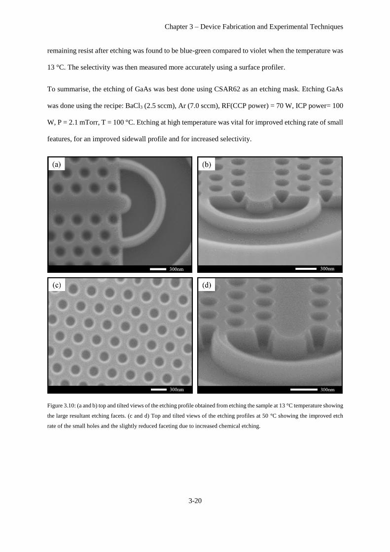
Chapter 3 – Device Fabrication and Experimental Techniques
3-20
remaining resist after etching was found to be blue-green compared to violet when the temperature was
13 °C. The selectivity was then measured more accurately using a surface profiler.
To summarise, the etching of GaAs was best done using CSAR62 as an etching mask. Etching GaAs
was done using the recipe: BaCl3 (2.5 sccm), Ar (7.0 sccm), RF(CCP power) = 70 W, ICP power= 100
W, P = 2.1 mTorr, T = 100 °C. Etching at high temperature was vital for improved etching rate of small
features, for an improved sidewall profile and for increased selectivity.
Figure 3.10: (a and b) top and tilted views of the etching profile obtained from etching the sample at 13 °C temperature showing
the large resultant etching facets. (c and d) Top and tilted views of the etching profiles at 50 °C showing the improved etch
rate of the small holes and the slightly reduced faceting due to increased chemical etching.

Chapter 3 – Device Fabrication and Experimental Techniques
3-21
Figure 3.11: The etching results obtained from etching at 100°C showing much better sidewalls from the top (a and b) and
tilted (c and d) view images showing optimised anisotropy of the etched sidewall profile in comparison to Figure 3.10.
Figure 3.12: (a) An optical microscope image showing the etched bright yellow region as an indicator of under etching
compared to the darker unetched regions. The figure also shows the etched trenches fabricated to allow larger surface contact
between the AlGaAs layer and the HF solution. (b) An optical microscope image of a group of PhC bridge structures, all had
successful wet etching without any bridge collapse.

Chapter 3 – Device Fabrication and Experimental Techniques
3-22
After dry etching the holes to the required depth of the bridges, hydrofluoric acid (HF) wet etching was
needed for removing the underlying Al0.8Ga0.2As layer (refer to Figure 3.9). It is expected that the
AlGaAs etch rate scales with the Aluminium to Ga ratio, in this case the ratio 0.8:0.2 of Al:Ga was
chosen from the literature20. It is important to have large etched features surrounding the PhC structure
to allow a higher surface area contact between the acid and the AlGaAs layer and allow better extraction
of etched AlGaAs fragments. Here, the dry etched sample is inserted into a 0.8:0.2 HF:DI solution for
10 seconds and subsequently rinsed in DI for 10 seconds. This process is repeated three times, before
finally rinsing the sample in IPA for 2 minutes20. Dividing the etching process into multiple etch and
rinse steps was found to help in extracting any remaining AlGaAs fragments from under the created
bridge. Interestingly, there were very few cases where a created bridge would collapse after etching the
underneath AlGaAs layer. This means that the PhC structure production yield is high and the structure
is mechanically robust. However, it is worth mentioning that when performing sonication on the etched
chip, even at very low powers, most of the created bridge on the chip collapsed and washed away. The
wet etched structures were inspected under the microscope and successful wet etching would typically
display bright yellow regions surrounding the etched structures due to the removed AlGaAs layer, see
Figure 3.12.
Numerical Modelling With Finite Difference Time
Domain
FDTD was the main tool used to simulate the photonic devices discussed in this thesis. These devices
were mainly the PhC components and the out-couplers. The software packages used were mainly Meep1
and Lumerical. It is beyond the scope of this thesis to dwell into the details of the theory and working
principles of FDTD. However, a brief summary will be given next to give the necessary introduction
for the very basics of FDTD as an electromagnetic wave simulation algorithm. For a comprehensive
presentation of the method and all of its technical aspects, the reader is referred to references 22 and 23.
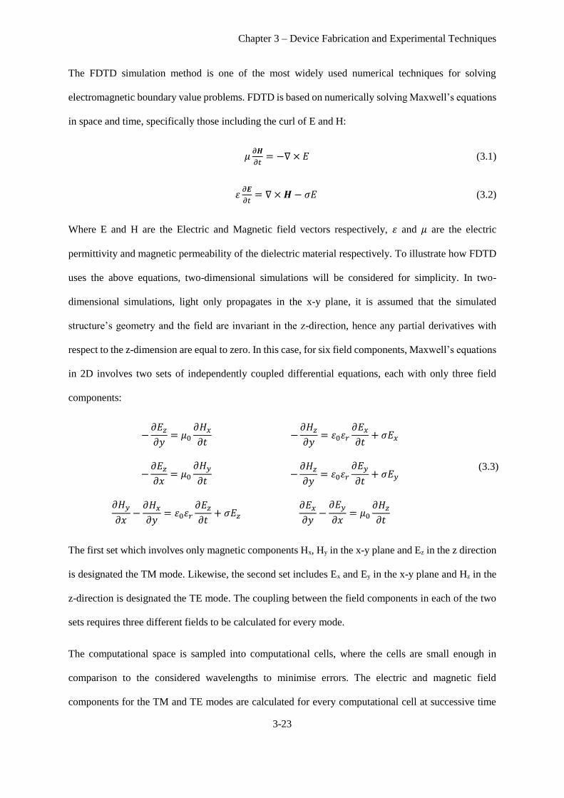
Chapter 3 – Device Fabrication and Experimental Techniques
3-23
The FDTD simulation method is one of the most widely used numerical techniques for solving
electromagnetic boundary value problems. FDTD is based on numerically solving Maxwell’s equations
in space and time, specifically those including the curl of E and H:
𝜇𝜕𝑯
𝜕𝑡= −∇ × 𝐸 (3.1)
𝜀𝜕𝑬
𝜕𝑡= ∇ × 𝑯 − 𝜎𝐸 (3.2)
Where E and H are the Electric and Magnetic field vectors respectively, 𝜀 and 𝜇 are the electric
permittivity and magnetic permeability of the dielectric material respectively. To illustrate how FDTD
uses the above equations, two-dimensional simulations will be considered for simplicity. In two-
dimensional simulations, light only propagates in the x-y plane, it is assumed that the simulated
structure’s geometry and the field are invariant in the z-direction, hence any partial derivatives with
respect to the z-dimension are equal to zero. In this case, for six field components, Maxwell’s equations
in 2D involves two sets of independently coupled differential equations, each with only three field
components:
−𝜕𝐸𝑧
𝜕𝑦= 𝜇0
𝜕𝐻𝑥
𝜕𝑡 −
𝜕𝐻𝑧
𝜕𝑦= 𝜀0𝜀𝑟
𝜕𝐸𝑥
𝜕𝑡+ 𝜎𝐸𝑥
−𝜕𝐸𝑧
𝜕𝑥= 𝜇0
𝜕𝐻𝑦
𝜕𝑡 −
𝜕𝐻𝑧
𝜕𝑦= 𝜀0𝜀𝑟
𝜕𝐸𝑦
𝜕𝑡+ 𝜎𝐸𝑦
(3.3)
𝜕𝐻𝑦
𝜕𝑥−
𝜕𝐻𝑥
𝜕𝑦= 𝜀0𝜀𝑟
𝜕𝐸𝑧
𝜕𝑡+ 𝜎𝐸𝑧
𝜕𝐸𝑥
𝜕𝑦−
𝜕𝐸𝑦
𝜕𝑥= 𝜇0
𝜕𝐻𝑧
𝜕𝑡
The first set which involves only magnetic components Hx, Hy in the x-y plane and Ez in the z direction
is designated the TM mode. Likewise, the second set includes Ex and Ey in the x-y plane and Hz in the
z-direction is designated the TE mode. The coupling between the field components in each of the two
sets requires three different fields to be calculated for every mode.
The computational space is sampled into computational cells, where the cells are small enough in
comparison to the considered wavelengths to minimise errors. The electric and magnetic field
components for the TM and TE modes are calculated for every computational cell at successive time
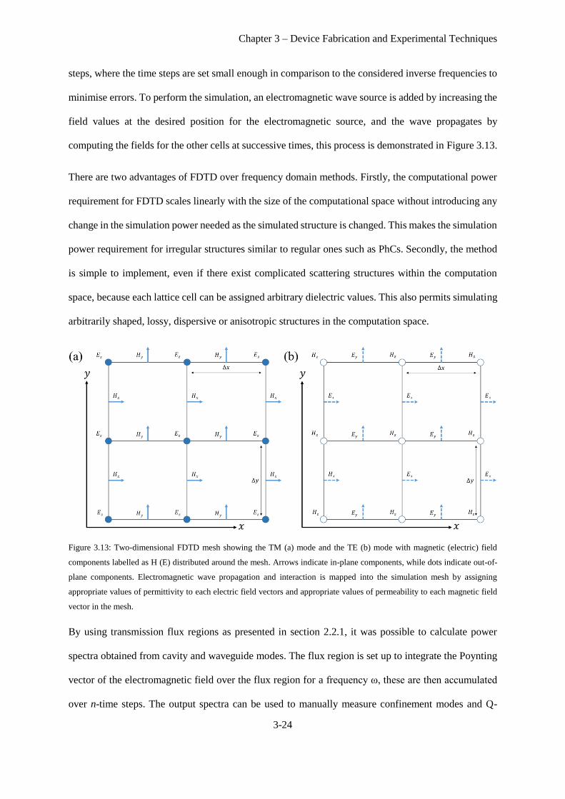
Chapter 3 – Device Fabrication and Experimental Techniques
3-24
steps, where the time steps are set small enough in comparison to the considered inverse frequencies to
minimise errors. To perform the simulation, an electromagnetic wave source is added by increasing the
field values at the desired position for the electromagnetic source, and the wave propagates by
computing the fields for the other cells at successive times, this process is demonstrated in Figure 3.13.
There are two advantages of FDTD over frequency domain methods. Firstly, the computational power
requirement for FDTD scales linearly with the size of the computational space without introducing any
change in the simulation power needed as the simulated structure is changed. This makes the simulation
power requirement for irregular structures similar to regular ones such as PhCs. Secondly, the method
is simple to implement, even if there exist complicated scattering structures within the computation
space, because each lattice cell can be assigned arbitrary dielectric values. This also permits simulating
arbitrarily shaped, lossy, dispersive or anisotropic structures in the computation space.
Figure 3.13: Two-dimensional FDTD mesh showing the TM (a) mode and the TE (b) mode with magnetic (electric) field
components labelled as H (E) distributed around the mesh. Arrows indicate in-plane components, while dots indicate out-of-
plane components. Electromagnetic wave propagation and interaction is mapped into the simulation mesh by assigning
appropriate values of permittivity to each electric field vectors and appropriate values of permeability to each magnetic field
vector in the mesh.
By using transmission flux regions as presented in section 2.2.1, it was possible to calculate power
spectra obtained from cavity and waveguide modes. The flux region is set up to integrate the Poynting
vector of the electromagnetic field over the flux region for a frequency ω, these are then accumulated
over n-time steps. The output spectra can be used to manually measure confinement modes and Q-

Chapter 3 – Device Fabrication and Experimental Techniques
3-25
factors. An alternative method to extract modes from the calculated spectra and measure their Q-factors
was using the harmonic inversion method that is embedded in the Meep package. For more details on
this method, the reader is referred to reference 21.
FDTD simulations with Meep were done using a computer cluster, known as high end computing
(HEC), and is operated by Linux. The HEC provided an abundance of memory and processing power
for simulations to be carried out with time efficiency. In most simulations, about 16 GB of memory was
used with up to 64 Intel cores clocked at 2.2 GHz. An example of a code used to simulate an optimised
L3 hole-type PhC cavity can be found in Appendix A. On the other hand, Lumerical was operated on a
windows workstation operated by an Intel Octa-core i7 processor with a Haswell microarchitecture.
The advantage that Lumerical provides over Meep is the visual interface of the simulation setup. This
is normally coded in Meep and required to be compiled before it can be visually inspected, consuming
a considerable amount of time. However, being able to run Meep in a Linux operation system make it
compatible with computer clusters, hence allowing simulations to run much faster when enough
processing resources are available.
Micro-Photoluminescence Spectroscopy
In this section, the methods for obtaining the μ-photoluminescence measurements are explained. The
measurement system was built in-house as shown in Figure 3.14. The excitation laser used in all the
measurements was a continuous wave Nd:YAG frequency doubled 532 nm laser. The beam is first
passed through neutral density (ND) filter wheels to control the incident power. The beam then passes
through a beam sampler where some of the light is reflected and measured by a photodiode power meter.
The laser is focused on the sample using a 50x objective lens with a numerical aperture of 0.65 such
that the laser spot size is reduced to approximately 1 μm2. The objective is mounted on a piezo controlled
xyz stage to allow fine tuning of the laser spot position. The emitted light is collected with the same
objective lens and directed to an Andor Shamrock 500 spectrometer for spectroscopic analysis. The
spectrometer uses a silicon electron-multiplying charge coupled device (EMCCD) for measurements
between 500-900 nm and an InGaAs array for measurements in the wavelength range 800-1600 nm.
Chapter 3 – Device Fabrication and Experimental Techniques
3-26
Both CCDs are Peltier cooled to -85 °C. For optical imaging purposes, the sample is illuminated with a
red LED and the image is collected from the objective lens and output to a computer screen via a USB
infrared camera.
Figure 3.14: The micro-photoluminescence setup used in taking the photoluminescence measurements in this thesis. The figure
shows the optical path of the laser as it goes to the sample and is reflected to the spectrometer. The laser light is attenuated
with neutral density (ND) filter wheels, a beam sampler is used to direct a portion of the light to a power meter, before reaching
the sample. The laser is focused with an objective lens which also collects emitted light by the sample and directs it toward
the spectrometer. The optical path of the illuminating red beam from the LED source to the digital camera that was used for
optical imaging can also be seen in the figure.

Chapter 3 – Device Fabrication and Experimental Techniques
3-27
Bibliography
1 A. F. Oskooi, D. Roundy, M. Ibanescu, P. Bermel, J. D. Joannopoulos, S. G. Johnson. MEEP: A
flexible free-software package for electromagnetic simulations by the FDTD method. Computer Physics
Communications, 181, 687-702 (2010)
2 M. J. Madou. Fundamentals of microfabrication: the science of miniturization, second edition.
Lithography, ch.1. CRC press (2002)
3 M. A. Mohammad, M. Muhammad, S. K. Dew, M. Stepanova. Fundamentals of electron beam
exposure and development. Nanofabrication, ch.2. Springer (2012)
4 S. Y. Chou, P. R. Krauss, P. J. Renstrom. Nanoimprint lithography. Journal of Vacuum Science &
Technology B, Nanotechnology and Microelectronics: Materials, Processing and Phenomena, 14, 4129-
4133 (1996)
5 V. Berger, O. Gauthier-Lafaye, E. Costard. Photonic band gaps and holography. Journal of Applied
Physics, 82, 60-64 (1997)
6 A. Heuberger. X-ray lithography. Journal of Vacuum Science & Technology B, Nanotechnology and
Microelectronics: Materials, Processing, Measurement, and Phenomena, 6, 107-121 (1988)
7 A. Bardea, N. Burshtein, Y. Rudich, T. Salame, C. Ziv, O. Yarden, R. Naaman. DNA and RNA
molecule detection and identification using a patterned capillary tube (PCT). Ann. Chem., 83, 9418-
9423 (2011)
8 R. Garcia, A. W. Knoll, E. Riedo. Advanced scanning probe lithography. Nature Nanotechnol., 9 577-
587 (2014)
9 R. C. Jaeger. Introduction to microelectronic fabrication, second edition. Volume 5. Film deposition,
ch.6. Upper Saddle River: Prentice Hall (2002)
10 K. H. Behrndt. Long-term operation of crystal oscillators in thin-film deposition. Journal of Vacuum
Science and Technology, 8, 622-626 (1971)
11 S. Franssila. Introduction to micro fabrication. Structures by deposition, ch.23. Wiley (2004)
12 W. P. McCray. MBE deserves a place in the history books. Nature Nanotechnol., 2, 259-261 (2007)
13 J. R. Creighton, P. Ho. Chemical vapor deposition. Introduction to chemical vapor deposition (CVD),
ch. 1. (2001)
14 V. A. Shchukin, D. Bimberg. Spontaneous ordering of nanostructures on crystal surfaces. Rev. Mod.
Phys., 71, 1125-1171 (1999)
15 S. Franssila. Introduction to micro fabrication. Structures by deposition, ch.11. Wiley (2004)
16 H. Jansen, H. Gardeniers, M. de Boer, M. Elwenspoek, J. Fluitman. A survey on the reactive ion
etching of silicon in microtechnology. Journal of Micromechanics and Microengineering, 6, 14-28
(1996)
17 M. D. Henry. ICP etching of silicon for micro and nanoscale devices. Doctorate thesis, California
Institute of Technology (2010)

Chapter 3 – Device Fabrication and Experimental Techniques
3-28
18 U. K. Khankhoje, S-H Kim, B. C. Richards, J. Hendrickson, J. Sweet, J. D. Olitzky, G. Khitrova, H.
M. Gibbs, A. Scherer. Modelling and fabrication of GaAs photonic-crystal cavities for cavity quantum
electrodynamics. Nanotechnology, 21, 065202 (2010)
19 CSAR 62 (AR-P 6200), Allresist, http://www.allresist.com/csar-62-ar-p-6200/ (last accessed
01/02/2017)
20 A. Faron. Locally controlled photonic crystal devices with coupled quantum dots: physics and
applications. Doctorate thesis, Stanford University (2009)
21 V. A. Mandelshtam, H. S. Taylor. Harmonic inversion of time signals and its applications. J. Chem.
Phys., 107, 6756-6769 (1997)
22 A. Taflove, S. C. Hagness. Computational Electrodynamics: The finite-difference-time-domain
method, third edition. Boston: Artech House (2005)
23 D. H. Choi, W. J. R. Hoefer. The Finite-difference-time-domain method and its application to
eigenvalue problems. IEEE Transactions on Microwave Theory and Techniques, 34, 1464-1470 (1986)

Chapter 4 – Photonic Crystals for Coupling to 2D Materials
4-1
Chapter 4
Photonic Crystals for Coupling to 2D
Materials
Introduction
Demonstrating reliable and miniaturised quantum light sources has been a major challenge in the past
couple of decades1. The realisation of such sources could resolve many challenges in creating integrated
quantum technology-based applications such as quantum key distribution and quantum computing2,3. A
brief introduction to single photon sources was presented in chapter 2. In this chapter of the thesis, the
strong potential for quantum light emission from 2D materials will be introduced. Following this, a
model for coupling transition metal dichalcogenides (TMDCs), a specific type of 2D material, to
resonant cavities based on photonic crystals (PhCs) is suggested. Numerical simulations using finite
difference time domain (FDTD) are used to prove that the suggested cavity design provides improved
light-matter interactions and enhancement in the light collection efficiency. In addition, analysis of the
reliability and robustness of the suggested design against fabrication and experimental uncertainties will
be carried out for claim support. Later, preliminary fabrication results of the suggested cavities and the
transfer of TMDC flakes on top, using both new and pre-developed techniques, will show the maturity
that this research direction has reached for realising chip-based quantum light emitters.

Chapter 4 – Photonic Crystals for Coupling to 2D Materials
4-2
TMDC Monolayers as Quantum Light Emitters
A dramatic increase in scientific research interest in 2D materials has taken place in the past decade due
to their extraordinary mechanical, electrical, thermal and optical properties4-7. For quantum technology
applications, their unique optical properties, particularly those based on transition metal dichalcogenide
materials, make them prospective candidates for single photon sources. Recently, multiple
demonstrations of single photon emission from defects in Tungsten Diselenide (WSe2) and MoS2 have
been reported using electrical and optical excitation8,9. Lattice defects in TMDC monolayers, such as
the ones shown in Figure 4.1 (b), can form localised electronic states inside the band gap of the TMDC
monolayer. These localised excitons, otherwise known as quantum dots (QDs) due to their zero-
dimensional confinement, appear with narrow linewidths in the optical photoluminescence signature of
the TMDC monolayers. On the other hand, impurities due to doping of the lattice, can have similar
optical properties and be harnessed in a similar fashion for quantum light applications.
Figure 4.1: (a) A schematic illustration of the atomic structure of a typical, (a) pure, (b) defective and (c) impure MoS2
monolayer flakes
Currently, a bottleneck for the application of 2D materials is their low optical absorption, quantum yield
and extraction efficiency of approximately a few percent. This severely reduces the luminescence
efficiency of light collected from these materials, hence reducing their potential optoelectronic
implementations10. Existing approaches to work around this issue are material specific, such as using
organic superacid to treat MoS211, using tunable Bragg mirrors for MoS2 and BN heterostructures and
enhancing the luminescence of MoS2 by fabricating plasmonic structures12,13. Therefore, a universal
approach that offers enhancement for all TMDCs would be advantageous in solving many issues related
(b) (a) (c)

Chapter 4 – Photonic Crystals for Coupling to 2D Materials
4-3
to light output from 2D materials. Using PhC cavities is one technique to improve light-matter
interactions and maximise light extraction.
Monolayer-cavity coupling has been demonstrated recently using a hole-type PhC14-17. Lasing and
enhancement in the spontaneous emission rate for light emitted from 2D materials has also been shown.
Whilst hole-type PhC cavities can have high Q-factors due to reduced mode loss in the vertical direction
due to the index contrast at the bridge-air interface, this method suffers from a few disadvantages. The
first is that the cavity mode is confined within the bridge structure comprising the high index region,
whereas TMDC surface emitter monolayers are conventionally exfoliated or wet transferred above this
structure. This causes reduced coupling between the emitter and the cavity mode’s maximum, leading
to lower light-matter interactions. The second disadvantage in using hole-type PhCs is that it results in
most of the cavity’s resonant mode being confined laterally within the high index slab, rather than
vertically coupled out of the plane to interact with the TMDC. This limits the collection efficiency of
light collected from these TMDC monolayers. Thirdly, the large dielectric-to-air volume ratio that exists
in the structures of hole-type PhCs results in undesirable light absorption by the dielectric material,
which is particularly critical when Si or GaAs is used as the dielectric material while the system
operation wavelength is in the visible regime. These disadvantages were the main motivation for
attempting to couple cavities and monolayer emitters using rod-type PhCs.
Using rod-type PhC cavities, the previously mentioned issues with hole-type PhCs can be solved, as
will be shown later. Similar to other forms of cavities, the suggested rod-type PhCs in this thesis
comprise a hexagonal array of rods with a lattice constant, a, and a rod radius, r. The cavity that will be
mainly discussed in this thesis is an H1 type of cavity where only one rod is missed from the structure
to create the localised state in the photonic bandgap of the lattice.
In previous work, carried out in Lancaster University, researchers have shown that 2D materials dip
when transferred onto hollowed regions such as etched trenches on a substrate18. In this work, we
suggest exploiting the flexible nature of TMDC monolayers to allow the dipping of a monolayer

Chapter 4 – Photonic Crystals for Coupling to 2D Materials
4-4
transferred onto a rod-type PhC to make it couple to the cavity’s centre region where the mode’s
antinode exists. Figure 4.2 shows an illustrative image of the suggested cavity design.
Interestingly, the reason behind choosing a hexagonal array PhC structure over the square array one is
due to the latter’s small radius pillar requirement which can become a limitation in the fabrication stage.
For rod-type cavities, square lattice arrays such as the one explained in reference 8, have been
extensively studied and a transverse magnetic (TM) bandgap has been shown. However, for
wavelengths in the visible regime such as those emitted by TMDC monolayers, the size of a square
lattice PhC designed to have its bandgap around this wavelength will require small dimensions
compared to a hexagonal lattice designed for the same wavelength range. For example, assume a square
lattice PhC is designed for molybdenum disulphide (MoS2), i.e. its bandgap range covers the central
emission wavelength of MoS2, which is approximately 660 nm, as shown in Figure 4.4 (a); an example
of a MoS2 flake is shown in Figure 4.4 (b). Kay et al. show that the for a PhC lattice of 𝑎 = 1 and 𝑟 =
0.2𝑎, an H1 cavity would have its cavity mode at 𝜆 = 2.56𝑎, in normalised units19. In other words, a
PhC cavity with a mode at 𝜆 = 660 𝑛𝑚, requires its lattice constant to be, 𝑎 = 258 𝑛𝑚 and the radius
to be, 𝑟 = 52 𝑛𝑚, with rod heights of at least 660 nm. Designing rods with such dimensions is very
challenging and requires an extremely accurate fabrication process. Furthermore, small fabrication
Figure 4.2: A schematics illustration of our suggested method for TMD-cavity coupling, showing the bowing of a monolayer
flake above a rod-type PhC cavity to allow optimised coupling to the centre of the cavity where the field maximum exists.

Chapter 4 – Photonic Crystals for Coupling to 2D Materials
4-5
uncertainties that changes the rod’s radius, the lattice constant, sidewall roughness and/or their vertical
height can shift the cavity mode and change its extraction efficiency. An H1 hexagonal lattice PhC
cavity of similar dimensions has its cavity mode at a much smaller wavelength. Making a cavity with a
mode wavelength of 660 nm makes it less dependent on fabrication limitations. The cavity suggested
in this work can achieve this goal using 𝑎 = 595 𝑛𝑚 and 𝑟 = 95 𝑛𝑚, over twice as large as the square
lattice crystal.
The PhC hexagonal lattice proposed in this work is surrounded by air for optimum index contrast. The
rods have a refractive index of 3.9, corresponding to the index of refraction for silicon at the MoS2
monolayer emission wavelength of approximately 660 nm. MoS2 was the material used for this work
because of its large neutral and charged exciton binding energies, making it a great candidate for room
Figure 4.3: (a) Our suggested cavity design, top and cross section screenshots from the modelling software showing the flux
region and the cavity structure. The lattice constant a is measured as the separation between the centres of two adjacent holes
in the lattice. B and c show the top and side views of the setup of the proposed rod type PhC cavity with the position of the
flux region above it. The simulation region is surrounded by a PML layer to prevent light reflection from the boundaries of
the simulation cell.
PML layers
Flux region
Silicon
(a) (b)
(c)
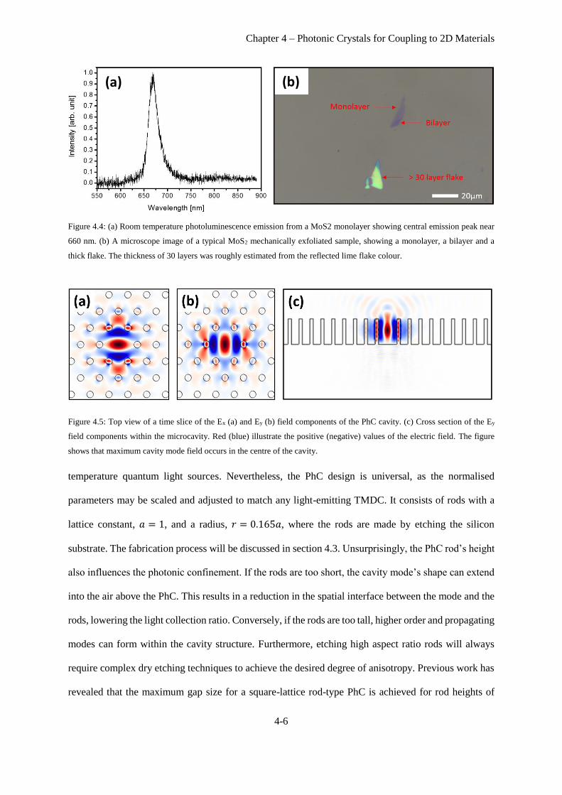
Chapter 4 – Photonic Crystals for Coupling to 2D Materials
4-6
Figure 4.4: (a) Room temperature photoluminescence emission from a MoS2 monolayer showing central emission peak near
660 nm. (b) A microscope image of a typical MoS2 mechanically exfoliated sample, showing a monolayer, a bilayer and a
thick flake. The thickness of 30 layers was roughly estimated from the reflected lime flake colour.
Figure 4.5: Top view of a time slice of the Ex (a) and Ey (b) field components of the PhC cavity. (c) Cross section of the Ey
field components within the microcavity. Red (blue) illustrate the positive (negative) values of the electric field. The figure
shows that maximum cavity mode field occurs in the centre of the cavity.
temperature quantum light sources. Nevertheless, the PhC design is universal, as the normalised
parameters may be scaled and adjusted to match any light-emitting TMDC. It consists of rods with a
lattice constant, 𝑎 = 1, and a radius, 𝑟 = 0.165𝑎, where the rods are made by etching the silicon
substrate. The fabrication process will be discussed in section 4.3. Unsurprisingly, the PhC rod’s height
also influences the photonic confinement. If the rods are too short, the cavity mode’s shape can extend
into the air above the PhC. This results in a reduction in the spatial interface between the mode and the
rods, lowering the light collection ratio. Conversely, if the rods are too tall, higher order and propagating
modes can form within the cavity structure. Furthermore, etching high aspect ratio rods will always
require complex dry etching techniques to achieve the desired degree of anisotropy. Previous work has
revealed that the maximum gap size for a square-lattice rod-type PhC is achieved for rod heights of
(a) (b)
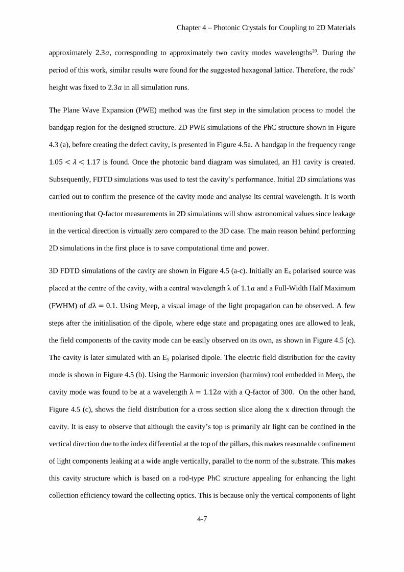
Chapter 4 – Photonic Crystals for Coupling to 2D Materials
4-7
approximately 2.3𝑎, corresponding to approximately two cavity modes wavelengths20. During the
period of this work, similar results were found for the suggested hexagonal lattice. Therefore, the rods’
height was fixed to 2.3𝑎 in all simulation runs.
The Plane Wave Expansion (PWE) method was the first step in the simulation process to model the
bandgap region for the designed structure. 2D PWE simulations of the PhC structure shown in Figure
4.3 (a), before creating the defect cavity, is presented in Figure 4.5a. A bandgap in the frequency range
1.05 < 𝜆 < 1.17 is found. Once the photonic band diagram was simulated, an H1 cavity is created.
Subsequently, FDTD simulations was used to test the cavity’s performance. Initial 2D simulations was
carried out to confirm the presence of the cavity mode and analyse its central wavelength. It is worth
mentioning that Q-factor measurements in 2D simulations will show astronomical values since leakage
in the vertical direction is virtually zero compared to the 3D case. The main reason behind performing
2D simulations in the first place is to save computational time and power.
3D FDTD simulations of the cavity are shown in Figure 4.5 (a-c). Initially an Ex polarised source was
placed at the centre of the cavity, with a central wavelength λ of 1.1𝑎 and a Full-Width Half Maximum
(FWHM) of 𝑑λ = 0.1. Using Meep, a visual image of the light propagation can be observed. A few
steps after the initialisation of the dipole, where edge state and propagating ones are allowed to leak,
the field components of the cavity mode can be easily observed on its own, as shown in Figure 4.5 (c).
The cavity is later simulated with an Ey polarised dipole. The electric field distribution for the cavity
mode is shown in Figure 4.5 (b). Using the Harmonic inversion (harminv) tool embedded in Meep, the
cavity mode was found to be at a wavelength λ = 1.12𝑎 with a Q-factor of 300. On the other hand,
Figure 4.5 (c), shows the field distribution for a cross section slice along the x direction through the
cavity. It is easy to observe that although the cavity’s top is primarily air light can be confined in the
vertical direction due to the index differential at the top of the pillars, this makes reasonable confinement
of light components leaking at a wide angle vertically, parallel to the norm of the substrate. This makes
this cavity structure which is based on a rod-type PhC structure appealing for enhancing the light
collection efficiency toward the collecting optics. This is because only the vertical components of light

Chapter 4 – Photonic Crystals for Coupling to 2D Materials
4-8
are allowed to leak upward, while components leaking at other angles are confined due to the photonic
band gap laterally and due to the high index contrast at the rods’ top-air interface. It is important to
mention here that absorption due to the dielectric material is not considered here. Absorption due to the
dielectric material is expected to reduce the cavity’s Q, however this becomes less important for low Q
cavities such as the ones shown here where the light escapes due to low confinement in the vertical
direction. This makes this technique potentially capable of enhancing light from quantum emitters to
be efficiently collected in the vertical direction by external collecting optics.
Measuring the enhancement in the light collection efficiency requires outputting the light flux spectrum
due to the cavity. This is then compared to the case when the source is placed directly above a substrate
without a PhC structure, representing a TMDC monolayer mechanically exfoliated directly on the
substrate. The enhancement ratio, 𝜂𝑒, is calculated as the power flux with and without the cavity
according to equation 1.
𝜂𝑒 = 𝑃𝑐𝑎𝑣/𝑃0 (1)
Figure 4.3 (b and c) shows screenshots taken directly from Lumerical’s user interface for the simulation
cells. The mesh resolution used in this simulation is 20 elements per lattice constant in every dimension.
Corresponding to approximately one element per 30 nm in real units. It was found that increasing the
number of elements does not add much more accuracy to the obtained results, hence the resolution was
fixed for all subsequent simulations at this value to save computation time and power. To measure the
enhancement in the light collection efficiency, the flux region was made to have an area of 23𝑎2 and
setup above the cavity, collecting light vertically radiated upward, mimicking an objective lens with
numerical aperture of 0.65.

Chapter 4 – Photonic Crystals for Coupling to 2D Materials
4-9
Figure 4.6: (a) FDTD simulations of the enhancement spectra for rods with a radius ranging from 0.155𝑎 and 0.170𝑎. (b)
Normalised flux spectrum for a crystal with radius 𝑟 = 0.161𝑎, in comparison with the emission from a source on a bulk
substrate, showing a 400% enhancement in the obtained flux.
When the source is placed directly on the substrate, a Gaussian curve corresponding to the dipole is
recorded by the flux region. Later, a series of simulations were carried out by having a source inside a
PhC cavity containing rods with different radii. The aim was primarily to investigate the robustness of
this design to fabrication imperfections that are likely to occur due to the relatively small structure.
Causes of shifts in the radius of the fabricated rods could be due to inaccurate selection of exposure
dosage in the electron-beam (e-beam) writing process. Other reasons could be due to non-anisotropic
sidewall profile development of the exposed regions of the resist, due to temperature variations of the
developing solution and/or the samples themselves. Hence, the radius was varied between 0.155𝑎 and
0.170𝑎. Maximum enhancement was achieved for a PhC cavity having rods with a radius, 𝑟 = 0.161𝑎,
where the cavity mode’s central wavelength, 𝜆 = 1.104𝑎, as shown in Figure 4.6 (a). The enhancement
obtained here is attributed to radiation modes from the cavity leaking vertically toward the flux region.
As the radius deviates from 𝑟 = 0.161𝑎, the collected power flux starts to decrease, reducing the
enhancement ratio, 𝜂𝑒. It is clear from Figure 4.6 to note that reducing the radius of the rods tends to
blue-shift the cavity mode’s energy, thus reducing its wavelength. This is expected, as the relationship
between the PhC’s cell radius, whether it is hole-type or rod-type, and the cavity mode’s energy was
anticipated through previous studies20. Figure 4.6 (b) plots a comparison between the obtained fluxes
for two cases. The first case is when a flake is exfoliated directly onto a flat substrate. The second case
is when the flake is transferred on top of the PhC structure, dipping to half the height of the rods where

Chapter 4 – Photonic Crystals for Coupling to 2D Materials
4-10
the cavity’s field maximum exists, as shown in in Figure 4.7. Later, the effect of having the source away
from the cavity’s centre will be discussed.
Figure 4.7: The cavity’s emitted flux spectra as the dipole position within the cavity is varied along the z-axis, where maximum
enhancement is obtained when the source is at a height, h/2. The enhancement reduces as the source height is varied along the
z-direction of the cavity. The figure on the right illustrates the degrees of bowing of the 2D material from the top of the rods
for each of the cases shown on the left.
Throughout the scope of this work, the simulations were ran assuming the flake is dipped to about half
the height of the rods. This is expected to be the ideal case since the source will be coupled to the field’s
antinode, creating maximum spatial coupling between the source and cavity. Dipping of the monolayer
to about half the height of the rods can promote the creation of defects due to strain, creating localised
excitons within the monolayer, however this might not be the case in reality and is discussed later in
the fabrication section. Performing simulations to anticipate the amount of dipping of a monolayer over
a typical structure depends on many factors. These include the monolayer material, the rods’ surface
roughness, and even the transfer temperature. These typically require setting up finite element
simulations whilst taking into account the van der Waals, Coulombic and gravitational force, which can
be exhaustive. Hence, a series of simulations were run with the dipole source emitter placed at different
heights along the vertical direction inside the cavity, to investigate the effect of dipping of the monolayer
emitter on the collection efficiency. Even though the source position in the vertical direction was
changed along the height of the cavity, it is important to mention that the flux region height above the
photonic structure was not changed. The cavity spectra for the different heights are shown in Figure

Chapter 4 – Photonic Crystals for Coupling to 2D Materials
4-11
4.7. It is expected that maximum Purcell enhancement for a light emitter should be achieved when the
source is spatially aligned with the cavity mode’s electric field maximum. This exists at the centre of
the cavity, one wavelength above the substrate, as was previously shown in Figure 4.5 (c). Enhancement
decreases as the source is moved toward the top of the rods due to reduced spatial coupling between the
emitter and the cavity mode, whilst also coupling to radiative modes in air. If the source is placed at the
bottom of the cavity, the main cause of reduction in enhancement is due to coupling to substrate-
mediated leaky modes.
Compared to H1 cavities, L3 cavities are usually favoured for better coupling to PhC waveguides, and
tend to have lower confinement quality factors of roughly 150. In L3 cavities, the enhancement in the
extraction efficiency is reduced due to non-vertical components of the cavity mode leaking at a wide
range of angles and missing the flux region.
Cavity Fabrication and Emitter Transfer
Fabricating hole-type PhCs has been achieved by many groups. This is due to its suitability in coupling
self-assembled QDs grown by the Stranski-Krastanov method to the cavity mode which is normally
confined within the bridge, where the dots normally exist (see chapter 3). Rod-type PhCs have been
fabricated and tested by fewer groups. Hence, much less literature was available to guide in the
fabrication steps of rod-type PhCs. This part of the chapter will explain the details for the approach
taken to fabricating this type of PhC.
Details of the working principles of the fabrication tools used in realising the rod-type PhC structure
are explained in chapter 3. While Silicon and GaAs have both similar refractive indices for light in the
visible regime, silicon was the substrate material used since it has a wider industrial use. The important
advantage Silicon holds over GaAs is the reduced electron and nuclear spin interaction in the optical
characteristics of single QDs. In addition to improved light collection efficiency, this is one of the future
research directions that this work can also lead to.

Chapter 4 – Photonic Crystals for Coupling to 2D Materials
4-12
The fabrication process starts with a (100) Silicon substrate with the oxide removed via HF etching.
The substrate is spin-coated with CSAR62 (AR-P 6200), which is a positive e-beam resist developed
by Allresist as a cheap alternative to ZEP520A. Compared to poly(methyl-methacrylate) (PMMA),
CSAR62 was found to achieve higher contrast and requires less exposure dosage, making the patterning
process much faster and more cost effective. In chapter 3, the advantage of the high selectivity to dry
etching that CSAR62 benefits from compared to PMMA was shown as a key factor for fabricating hole-
type PhCs. The resist material is usually diluted in a 1:1 ratio of CSAR62:Anisole to reduce the
concentration and allow thin film spin coating. It is important to choose the film thickness wisely, since
there will be a hard mask metal lift-off process that will take place after the e-beam exposure. A rule of
thumb known in the industry is that there needs to be a minimum of a 3:1 thickness ratio between the
resist and the lift-off metal. Spinning too thin a layer will cause the lift-off process to fail, on the other
hand, spinning a thick layer will reduce the contrast of the achieved pattern. Producing high contrast
patterns is especially important in this work since the cavity mode’s central wavelength and extraction
efficiency are directly related to the fabricated radius of the rods. The thickness used for realising the
structure was thus 120 nm. The spin-coated sample is subsequently baked on a hot plate at 180 °C for
3 minutes.
The mask was designed with AutoCAD and corrected with BEAMER to reduce proximity effects. The
pattern writing was done with a 50kV JEOL (JBX-5500ZD) using a beam current of 50 pA and an
exposure dosage of 120 μC/cm2. The pattern was later developed with o-xylene for 140 s, during which
gentle sonication took place for 15 s. It was found that gently sonicating the sample while it is in the
developing solution helps removing the exposed resist layer completely, until the substrate is exposed
to air. The issue of partial development of the resist is more prominent with PMMA for small features,
such as those found in fabricating the hole-type PhC structure, as was shown in chapter 3. This was
another advantage for using CSAR62 over PMMA.
During the period of this work, many tests were carried out to identify the material that acts as the best
hard mask for dry etching Silicon using Reactive Ion Etching (RIE). A judgement was made based on

Chapter 4 – Photonic Crystals for Coupling to 2D Materials
4-13
the etching selectivity and the ease of pattern transfer through the lift-off process. Using the dry etching
recipe developed during this work (which will be explained later), the selectivity achieved in etching
Silicon with an Aluminium hard mask was 13:1. Nickel was found to have a selectivity of 18:1, whilst
with Chromium the selectivity was 49:1. Previous work has shown high selectivity in etching Si using
SiO2, where it was calculated that the selectivity can range from 5-35:1 depending on the etching
recipe21. Hence, efforts were primarily focused toward transferring the pattern to the substrate using Cr
as a hard mask.
To measure the etching selectivity, a Veeco AFM CP-II was used. The resist thickness was measured
after spinning using the developed patterns. After etching, another measurement was made to measure
the sum of the etch depth and the remained resist. Finally the resist is stripped off the substrate and the
actual etch depth was measured. Given the etch time period, this set of measurements can be used to
calculate the etch rate of the resist and the etch rate of the semiconductor, hence the selectivity.
Cr is bought attached to a tungsten wire from which it can sublimate when a current of 60-70 A and a
voltage of 2 V is applied at 10-6 Pa. Importantly, the desired rod height should be approximately 2.25
times the lattice constant for a maximum Q-factor and extraction efficiency20. In this case, the rods
should be etched by approximately 1320 nm, for efficiently coupling the cavity to a MoS2 monolayer
that has a central emission wavelength of 660 nm. With a 49:1 selectivity, the Cr thickness should be
at least 27 nm. However, to ensure enough Cr is available for the etching process, the metal thickness
was made approximately 40 nm. This is the reason that the resist thickness was targeted for 120 nm, to
follow the 3:1 resist:metal lifeoff rule of thumb.
The lift-off process was done in PG remover 1165, which is a mixture of pure organic materials
including N-methyl-2-pyrrolidine, compatible with many metals including Chromium and
manufactured by Microposit. The sample is inspected under a long working distance objective to
identify if the lift-off process was successful. Sonication is usually desirable if the lift-off process took
more than 24 hours to remove any remained resist quickly. However, it was found that sonicating for
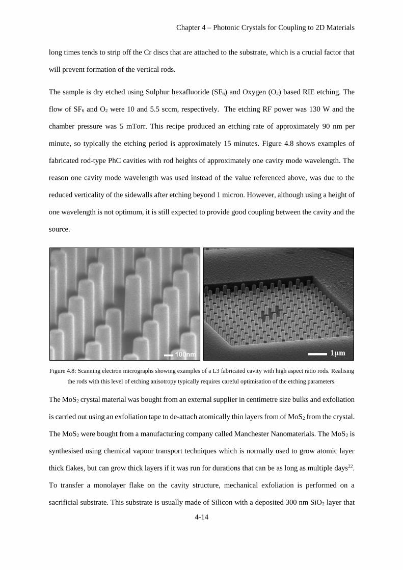
Chapter 4 – Photonic Crystals for Coupling to 2D Materials
4-14
long times tends to strip off the Cr discs that are attached to the substrate, which is a crucial factor that
will prevent formation of the vertical rods.
The sample is dry etched using Sulphur hexafluoride (SF6) and Oxygen (O2) based RIE etching. The
flow of SF6 and O2 were 10 and 5.5 sccm, respectively. The etching RF power was 130 W and the
chamber pressure was 5 mTorr. This recipe produced an etching rate of approximately 90 nm per
minute, so typically the etching period is approximately 15 minutes. Figure 4.8 shows examples of
fabricated rod-type PhC cavities with rod heights of approximately one cavity mode wavelength. The
reason one cavity mode wavelength was used instead of the value referenced above, was due to the
reduced verticality of the sidewalls after etching beyond 1 micron. However, although using a height of
one wavelength is not optimum, it is still expected to provide good coupling between the cavity and the
source.
Figure 4.8: Scanning electron micrographs showing examples of a L3 fabricated cavity with high aspect ratio rods. Realising
the rods with this level of etching anisotropy typically requires careful optimisation of the etching parameters.
The MoS2 crystal material was bought from an external supplier in centimetre size bulks and exfoliation
is carried out using an exfoliation tape to de-attach atomically thin layers from of MoS2 from the crystal.
The MoS2 were bought from a manufacturing company called Manchester Nanomaterials. The MoS2 is
synthesised using chemical vapour transport techniques which is normally used to grow atomic layer
thick flakes, but can grow thick layers if it was run for durations that can be as long as multiple days22.
To transfer a monolayer flake on the cavity structure, mechanical exfoliation is performed on a
sacrificial substrate. This substrate is usually made of Silicon with a deposited 300 nm SiO2 layer that
Chapter 4 – Photonic Crystals for Coupling to 2D Materials
4-15
covers it. The SiO2 layer plays a vital role in providing enhanced optical contrast for finding exfoliated
monolayers under the optical microscope. Using the Si/SiO2 substrate, Polyvinyl Alcohol (PVA) is
spin-coated at 2000 rpm to create a layer approximately 100 nm in thickness. Subsequently, PMMA is
spin-coated on top of the PVA layer at 4000 rpm and baked at 150 °C to create a layer with a thickness
of 200 nm. Finally, the desired TMDC is mechanically exfoliated and transferred to the
Si/SiO2/PVA/PMMA stack. Monolayers are then visually identified under an optical microscope and
those that look similar in colour and brightness to that shown in Figure 4.4 (b) are prepared for transfer.
The flake is transferred using the wet transfer process, which involves stamping the flake over the
cavity23. A schematic of the wet transfer process is shown in Figure 4.9. Trenches are etched around the
monolayer to create an isolated island using a sharp pointer pin that scratches through the PVA and
PMMA. Water droplets are allowed in the trenches to dissolve the sacrificial PVA layer and let the top
PMMA layer float on the water. The sample is then immersed in a water bath such that the PMMA
layer detaches from the sample and floats on the surface of the bath, isolating the PMMA layer. The
floating PMMA film is scooped from the water surface using a metal washer ring and the washer is
placed on a hot plate to allow adhesion between the PMMA layer and the washer. The washer is flipped
and mounted on a tool made in-house to allow clipping of the washer to a slow descending arm which
lowers the washer/PMMA toward the sample. A microscope is used to align the flake on top of the
cavity before mounting. It is desirable to have the sample on a hotplate before the actual transfer to
improve adhesion between the flake and the cavity. Figure 4.10 shows the initial results achieved in
transferring monolayers of MoS2 onto rod-type PhC cavities.
Room temperature μ-photoluminescence measurements of the sample shown in Figure 4.8 did not show
any cavity enhancement to the emission of the MoS2 monolayer, the emission obtained is shown in
Figure 4.11. The figure shows a strong bi-layer emission with a peak central wavelength of 810 nm and
a weaker monolayer emission around 660 nm, without any indication of cavity mode coupling11. SEM
imaging proves that this is caused due to miss-alignment of the flake as it was transferred above the
cavity which can be observed in Figure 4.10 (b).

Chapter 4 – Photonic Crystals for Coupling to 2D Materials
4-16
Figure 4.9: A schematic illustration of the steps involved in the dry transfer technique. (a) The initial structure of the wet
transfer is made of Si with PVA and PMMA spin coated on the substrate and the flake exfoliated on top of the structure. (b)
Trenches are made and water droplet are allowed passed through the trenches to allow dissolving the PVA layer. (c) The
PMMA layer together with the flake are detached from the wafer and float on a water bath. (d) The PMMA layer is then
scooped out of the bath and stamped on the rods structure.
Figure 4.10: Scanning Electron Micrographs showing initial results from transferring monolayer flakes on top of a fabricated
PhC cavity made in silicon by e-beam lithography and dry RIE etching. The figures shows how the topology of a flake can be
varied by the structure of its hosting substrate. This was an initial attempt though, perfect alignment of a flake above a cavity
was not achieved.
(b)
(d) (c)
Flake PMMA PVA Silicon Water
(a)

Chapter 4 – Photonic Crystals for Coupling to 2D Materials
4-17
Figure 4.11: Room temperature μ-photoluminescence emission from the MoS2 flake shown in Figure 4.10 excited with a laser
power of 3 mW. The sample was placed under vacuum in the order of 10-3 mtorr to ensure that the cavity surrounding has a
refractive index of as close to 1 as possible, matching that of the simulated cavity. The figure shows emission signatures of a
monolayer and a bilayer corresponding to central wavelengths of 660 and 810 nm.
Conclusions
In conclusion, a model was proposed to couple 2D material-based light emitters to a resonant cavity
efficiently. The model that was proposed which is based on rod-type PhCs provides advantages over
current methods for 2D material-cavity coupling. These advantages include spatial coupling between
the field’s maximum and the quantum emitter and improved light collection efficiency from these
cavities. The photonic band diagram for the designed structure was solved and the field distribution
within an H1 cavity was simulated. Simulations of the collected flux spectra was measured for a range
of PhC rod radii and maximum enhancement in the collection efficiency of about 400% was shown for
𝑟 = 0.161𝑎. A series of simulations were carried out to investigate the effect of having the monolayer
dipping at different heights inside the cavity. It was shown that maximum enhancement is achieved
when the source spatially overlaps with the cavity mode’s maximum and reduces as the source is moved
up or down from the cavity due to reduced spatial coupling and coupling to leaky modes outside the
cavity, respectively.

Chapter 4 – Photonic Crystals for Coupling to 2D Materials
4-18
Details of the fabrication process of these PhCs were explained and preliminary results were shown.
The method of transferring monolayers on the cavity and the results achieved were demonstrated.
Enhancing the collection efficiency further could be done using the author’s recent work in Solid
Immersion Lenses24,25. Glass SILs can be reliably positioned on top of the cavities with micrometer-
scale accuracy. These kind of SILs were shown to give over 300% enhancement in the light collection
efficiency. While SILs made of other materials such as GaAs can achieve over 1000% enhancement as
discussed in reference 24. Combining SILs with the PhC cavities can lead to a greater increase in the
light collected from TMDC monolayers. Another advantage in placing a SIL on top of the cavity can
be enhancing the vertical confinement due to total internal reflection at the air-glass interface. Initial
results from FDTD simulations show that adding a slab with a similar refractive index to that of glass
showed that the cavity’s Q-factor can be increased by four folds.

Chapter 4 – Photonic Crystals for Coupling to 2D Materials
4-19
Bibliography
1 M. D. Eisaman, J. Fan, A. Migdall, S. V. Polyakov. Single-photon sources and detectors. Rev. Sci.
Instrum., 82, 071101 (2011)
2 N. Gisin, G. Ribordy, W. Tittel, H. Zbinden. Quantum cryptography. Rev. Mod. Phys., 74, 145-195
(2002)
3 T. D. Ladd, F. Jelezko, R. Laflamme, Y. Nakamura, C. Monroe, J. L. O’Brien. Quantum computers.
Nature, 464, 45-53 (2010)
4 D. Akinwande, C. Brennan, J. Scott Bunch, et al.. A review on mechanics and mechanical properties
of 2D materials-Graphene and beyond. Extreme Mechanics Letters, 13, 42-77 (2017)
5 D. Wei, Y. Liu, Y. Wang, H. Zhang, L. Huang, G. Yu. Synthesis of N-doped Graphene by chemical
vapour deposition and its electrical properties. Nano Lett., 9, 1752-1758 (2009)
6 A. A. Balandin. Thermal properties of graphene and nanostructured carbon materials. Nature Mater.,
10, 569-581 (2011).
7 F. Xia, H. Wang, D. Xiao, M. Dubey, A. Ramasubramaniam. Two-dimensional material
nanophotonics. Nature Photon., 8, 899-907 (2014)
8 C. P. Berraquero, M. Barbone, D. M. Kara, G. Ilya, D. Yoon, A. K. Ott, J. Beitner, K. Watanabe, T.
Waniguchi, A. C. Ferrari, M. Atature. Atomically thin quantum light emitting diodes. Nature Commun.,
12978 (2016)
9 C. Chakraborty, L. Kinnischtzke, K. M. Goodfellow, R. Beams, A. N. Vamivakas. Voltage-controlled
quantum light from an atomically thin semiconductor. Nature Nanotechnol., 10, 507-511 (2015)
10 K. R. Paton, J. N. Coleman. Relating the optical absorption coefficient of nanosheet dispersion to the
intrinsic monolayer absorption. arXiv:1511.04410 (2015)
11 M. Amani, D. H. Lien, D. Kiriya, et al.. Near-unity photoluminescence quantum yield in MoS2.
Science, 4, 1065-1068 (2015)
12 S. Dufferwiel, S. Schwarz, F. Withers, et al. Exciton-polaritons in van der Waals heterostructures
embedded in tunable microcavities. Nature Commun., 6, 9576 (2015)
13 K. C. J. Lee, Y. Chen, H. Lin, C. Cheng, P. Chen, T. Wu, M. Shih, K. Wei, L. Li, C. Chang. Plasmonic
gold nanorods coverage influence on enhancement of the photoluminescence of two-dimensional MoS2
monolayer. Sci. Rep., 5, 16374 (2015)
14 S. Wu, S. Buckley, A. M. Joes, J. S. Ross, N. J. Ghimire, J. Yan, D. G. Mandrus, W. Yao, F. Hatami,
J. Vuckovic, A. Majumdar, X. Xu. Control of two-dimensional excitonic light emission via photonic
crystal. IOP 2D Mater., 1, 011001 (2014)
15 X. Gan, Y. Gao, K. F. Mak, X. Yao, R. Shiue, A. Van der Zande, M. E. Trusheim, F. Hatami, T. F.
Heinz, J. Hone, D. Englund. Controlling the spontaneous emission rate of monolayer MoS2 in a
photonic crystal nanocavity. Appl. Phys. Lett., 103, 181119 (2013)
16 Y. Ye, Z. J. Wong, X. Lu, H. Zhu, X. Chen, Y. Wang, X. Zhang. Monolayer exciton laser. Nature
Photon., 9, 733-737 (2015)

Chapter 4 – Photonic Crystals for Coupling to 2D Materials
4-20
17 S. Wu, S. Buckley, J. R. Schaibley, L. Feng, J. Yan, D. G. Mandrus, F. Hatami, W. Yao, J. Vuckovic.
Monolayer semiconductor nanocavity laser with ultralow thresholds. Nature, 520, 69-72 (2015)
18 N. D. Kay, B. J. Robinson, V. I. Falko, K. S. Novoselov, O. V. Kolosov. Electromechanical sending
of substrate charge hidden under atomic 2D crystals. Nano Lett, 14 (6), 3400-3404 (2014)
19 P. R. Villeneuve, S. Fan, J. D. Joannopoulos. Microcavities in photonic crystals: mode symmetry,
tunability, and coupling efficiency. Phys. Rev. B, 54, 7837-7842 (1996)
20 C. Gui, Y. Zhang, J. Du, J. Xia, J. Wang. Experimental demonstration of analog signal transmission
in a silicon photonic crystal L3 resonator. Optics Express, 23, 13916-13923 (2015)
21 N. R. Rueger, M. F. Doemling, M. Schaepkens, J. J. Beulens, T. E. F. M. Standaer, G. S. Oehrlein.
Selective etching of SiO2 over polycrystalline silicon using CHF3 in an inductively coupled plasma
reactor. Optics Express, 23, 13916-13923 (2015)
22 R. Roldan, A. Castellanos-Gomez, E. Cappelluti, F. Guinea. Strain engineering in semiconducting
two-dimensional crystals. J. Phys.: Condens. Matter, 27, 313201 (2015)
23 A. Castellanos-Gomez, M. Buscema, R. Molenaar, V. Singh, L. Janssen, H. S. J. Van der Zant, A. G.
Steele. Deterministic transfer of two-dimensional materials by all-dry viscoelastic stamping. IOP 2D
Mater, 1, 011002 (2014)
24 C. S. Woodhead, J. Roberts, Y. J. Noori, Y. Cao, R. Bernardo-Gavito, P. Tovee, A. Kozikov, K.
Novoselov, R. J. Young. IOP 2D Mater., 4, 015032 (2016)
25 K. A. Serrels, E. Ramsay, P. A. Dalgarno, B. D. Gerardot, J. A. O’Connor, R. H. Hadfield, R. J.
Warburton, D. T. Reid. Solid immersion lens applications for nanophotonic devices. J. Nano-photonics,
2, 021854 (2008)

Chapter 5 – Deterministic Positioning of III-V Nanowires on Silicon for Photodetector Applications
5-1
Chapter 5
Catalytic Free Deterministic Positioning of
III-V Nanowires on Silicon for
Photodetector Applications
Introduction
Avalanche photodetectors (APDs) exploit the photoelectric effect to convert photons incident on a
photodiode into small electrical pulses that are strengthened by avalanche multiplications to make them
measurable by modern electronic counters1,2. As discussed previously in chapter 2, a semiconductor
avalanche photodetector is a p-i-n junction that is reverse biased under high voltages, but not higher
than their breakdown voltages. When a photon is absorbed by the intrinsic region, an electron-hole pair
is created. The electron and hole are subsequently separated and accelerated by the electric field to the
n and p sides, respectively. This causes other electron-hole pairs to be created due to the high kinetic
energy that the initial electron-hole pair exhibits due to the applied electric field. Although state-of-the-
art APDs have a higher dark current and lower quantum efficiency compared to superconducting
nanowire detectors, APDs do not require cryogenic temperatures and can operate reasonably well at
practically achievable temperatures for use in applications such as Quantum Key Distribution (QKD).
Despite the differences in the fabrication and integration complexity, both of the previously mentioned
technologies for single photon detection can be integrated. Although, one is more efficient, has a higher
signal to noise ratio, but requires cryogenic temperatures and is expensive to run, while the other is less

Chapter 5 – Deterministic Positioning of III-V Nanowires on Silicon for Photodetector Applications
5-2
efficient but can operate at low temperatures achievable by thermoelectric coolers. The current effort is
directed toward realising a room temperature SPD that has a high quantum efficiency and small dark
current for faster QKD bit rates and more practical quantum technology applications.
In recent years, III-V semiconductor nanowires have attracted much attention as potential building
blocks for a variety of basic optical components including solar cells, frequency electronics, single
photon sources and photodetectors3-10. Nanowires are traditionally chemically synthesised, or grown by
epitaxial means using vapour-liquid-solid methods, where the latter has the advantage of realising
nanowires with much lower impurities that may otherwise cause atomic defects to appear in the crystal
lattice structure. While silicon is the most universally used material in the electronics industry,
integration of III-V semiconductors onto Si can result in compact integrated optoelectronic circuits.
However, current III-V semiconductor devices, such as photodiodes, image sensors and lasers, are
fabricated via a hybrid bonding of III-V bulk substrates onto complementary metal oxide semiconductor
(CMOS) integrated circuits11,12. This bonding process can drastically limit the minimum size of the
device and entails a large increase in production costs. To solve this issue, epitaxial integration of III-
V semiconductor optoelectronics onto the Si platform can ease large-scale integration and reduce
production costs13,14.
Compared to thin film photodetectors, reports have shown that ultra-high photocurrent gains are
achievable using GaN p-i-n nanowire based photodetectors, which is three orders of magnitude higher
than for those that use thin film structures15. Moreover, their InAs counterparts have been reported to
exhibit high photoresponsivity at the C-band telecommunication wavelength16,17. Also, core-shell
GaAs/AlGaAs nanowire photodetectors were shown to have a response time of only a picosecond,
making them suitable for high speed performance photodetectors18. Core-shell InAs/InP nanowires, on
the other hand, were reported to have a very high mobility at room temperature19. In addition to the
ultra-high photocurrent gain, higher photo-responsivity, shorter response time and higher mobility, the
photonic absorption of nanowire arrays has been increased, by optimising the nanowire’s length and
diameter, to levels matching those for planar device photodetectors, despite having 10% the volume.
The attractive structural aspect of nanowires that makes them advantageous over planar structures is

Chapter 5 – Deterministic Positioning of III-V Nanowires on Silicon for Photodetector Applications
5-3
their wider light collection angle. This increases the probability that an impinging photon on the
nanowire at a wide range of angles can be absorbed and converted to an electric current.
The operation temperature of photodetectors is crucial for integrated photonic applications, where the
cooling systems can limit the size of the overall device and increase its power requirements. It has been
shown recently that adding Sb as a group V material together with As during epitaxial growth of InAs
nanowires allows the realisation of low leakage current p-i-n nanowires for photodetection applications
at room temperature20. Furthermore, incorporating Sb can improve the nanowire crystal quality and
reduce the stacking fault density. Sourribes et al. observed a sharp decrease in the stacking fault density
by increasing the Sb content up to 15%, while increasing the field effect mobility by more than three
times21. These advantages can in practice make nanowire based photodetectors a promising approach
that can offer better photodetection solutions in comparison to their planar thin film counterparts.
A wide range of operation wavelengths within the near-infrared spectrum can be achieved for nanowire
photodetectors. By tuning the temperature and the material composition that forms the nanowires, the
operation wavelength can be tuned. For example, by doping InAs with Sb, the bandgap of the material
can be reduced, hence red-shifting the operation wavelength20. In addition, other semiconductor
materials such as GaAs and InP can be exploited to realise nanowire-based photodetectors that can
operate at other wavelengths such as those in the popular C-band and O-band of the telecommunications
spectrum. Developing photon detectors in these frequency ranges is essential since long distance fibre
optic telecommunications are solely operated in these bands where fibre attenuation is minimum. The
attractive low leakage current achieved previously with InAs nanowires photodetectors together with
the high bandgap property of GaAs for room temperature telecom wavelength single photon detection,
make these materials attractive for studying in this work.
There are two common methods of biasing a p-i-n nanowire before using it for photodetection
applications. The first is done by fabricating metal contacts and placing a nanowire horizontally on the
substrate such that each end of the nanowire is connected to a contact pad, as shown in Figure 5.1:. The
second is achieved by fabricating contacts on top of a free-standing nanowire grown on a doped
substrate used as the back contact, as shown in Figure 5.2. The first method suffers from many problems.

Chapter 5 – Deterministic Positioning of III-V Nanowires on Silicon for Photodetector Applications
5-4
Firstly, the nanowires are usually grown free-standing on a substrate using MBE, PECVD and detached
from the substrate by sonicating the substrate in a solution. The wires are then drop cast on a substrate
and the solution is allowed to dry, which leaves the nanowires randomly distributed. Spatially
positioning the nanowires at a desired location can be done using probe techniques, but is extremely
difficult and not scalable enough to be adapted for mass manufacturing. This is especially the case when
multiple nanowires are needed to be biased in a nanowire photodetector array. Secondly, there isn’t an
effective method to optically couple a nanowire photodetector in this form to an integrated waveguide,
but can be coupled better to vertical light illumination. On the other hand, exploiting free-standing
nanowires for photodetector applications, as shown in Figure 5.2:, can provide many advantages. First,
this method can benefit from the advantage of deterministic positioning of nanowires on a substrate by
patterning and etching a layer of SiO2 on a Si substrate, this method will be explained in detail later.
Second, a large grid of nanowires can be biased simultaneously using contacts fabricated with more
scalable techniques such as photolithography. Thirdly, a nanowire array biased in this form can be
fabricated and coupled efficiently to a PhC waveguide with a tapered mode out-coupler, as shown in
Figure 5.3. Using a top gold contact is advantageous for reflecting light travelling away from the
nanowire, therefore realising better light confinement within the SU8 layer. Alternatively, an optically
transparent Ohmic contact material such as indium tin oxide can be used if light incident on the
photodetector is coupled vertically.
Figure 5.1: Biasing a nanowire that lies horizontally on a substrate with each end connected to one contact pad, where the light
is typically applied from above the substrate. The nanowire is broken off its growth substrate by sonication and transferred on
a pre-patterned substrate using the drop casting method.

Chapter 5 – Deterministic Positioning of III-V Nanowires on Silicon for Photodetector Applications
5-5
Figure 5.2: Biasing a free-standing nanowire grown with MBE by etching a hole on the SiO2 layer and exposing the Si substrate
to allow the nanowire to seed. The top gold contact is patterned on an optically transparent material such as SU8 after dry
etching a portion of it to expose the top of the N-type region of the nanowire.
Figure 5.3: A suggested example for coupling a PhC waveguide to a p-i-n nanowire photodetector using a tapered out-coupler
that direct the light beam from the photonic waveguide toward the intrinsic region of the nanowire.
This chapter will firstly present a simple and effective method to deterministically position III-V
material nanowires on a silicon substrate, a potential technique for large scale integration of nanowire-
based photodetectors in photonic chips. An effective approach toward fabricating the nanowire sites
using electron-beam (e-beam) lithography and chemical wet etching is also presented. Later, results
from growing nanowires and the effect of changing the MBE growth temperature on InAs nanowire
formation is explored. Results will also be presented from using the same method to selectively grow
GaAs nanowires together with preliminary photoluminescence measurements results.
Chapter 5 – Deterministic Positioning of III-V Nanowires on Silicon for Photodetector Applications
5-6
Site-Controlled Nanowire Fabrication
Epitaxial and synthetic growth of nanowires on a substrate is normally a random process where the
nanowires grow uniformly across a substrate. The growth density depends on many parameters such as
the substrate’s temperature and the abundance of the nanowire composition material in the chamber.
Nanowire growth engineering for integrated photonic detectors requires deterministic positioning of the
nanowires with a spatial accuracy that is smaller than the system’s operation wavelength for an
optimised signal collection efficiency. Moreover, nucleation of nanowires on a flat substrate often
requires metal alloy seeding to catalyse the growth. However, intense research efforts are currently
underway to develop catalyst-free growth techniques, hence avoiding metal contamination whilst
favouring full compatibility with Si technology20. The effect of metal incorporation into the nanowire
during growth has adverse effects on the optical and electrical properties of the devices, as presented in
multiple reports22-25. In addition, avoiding metal seeding reduces the number of technological steps
needed to realise the nanowires. The results shown in this chapter include the catalyst-free growth
seeding of III-V nanowires on Si substrates.
Integrating high performance III-V nanowires with mainstream Si technology encounters many long-
term challenges due to the lattice mismatch, different crystal structures and thermal coefficients. While
this process of spatial growing of III-V material nanowires is done on Si, the results presented here can
be improved if a lattice-matched III-V material is used as the host substrate. In this work, all the Si
substrates used as hosts for the nanowires are p-type (111) with a thermally grown 25 nm SiO2 coating.
The mask for the nanowire sites constitutes primarily of circularly shaped 50 nm diameter holes etched
into the SiO2 layer until the Si substrate is exposed. Across the mask, different arrays containing
different hole diameters and a varying pitch were used to investigate the effect of the resultant
structure’s geometry on the formed pattern and the growth ratio of nanowires in these holes. Figure 5.4
shows sections of the mask used in this process. Because the mask contains regions with arrays of
varying hole density, proximity effect correction was vital to ensure the dosage distribution was uniform
throughout the mask.
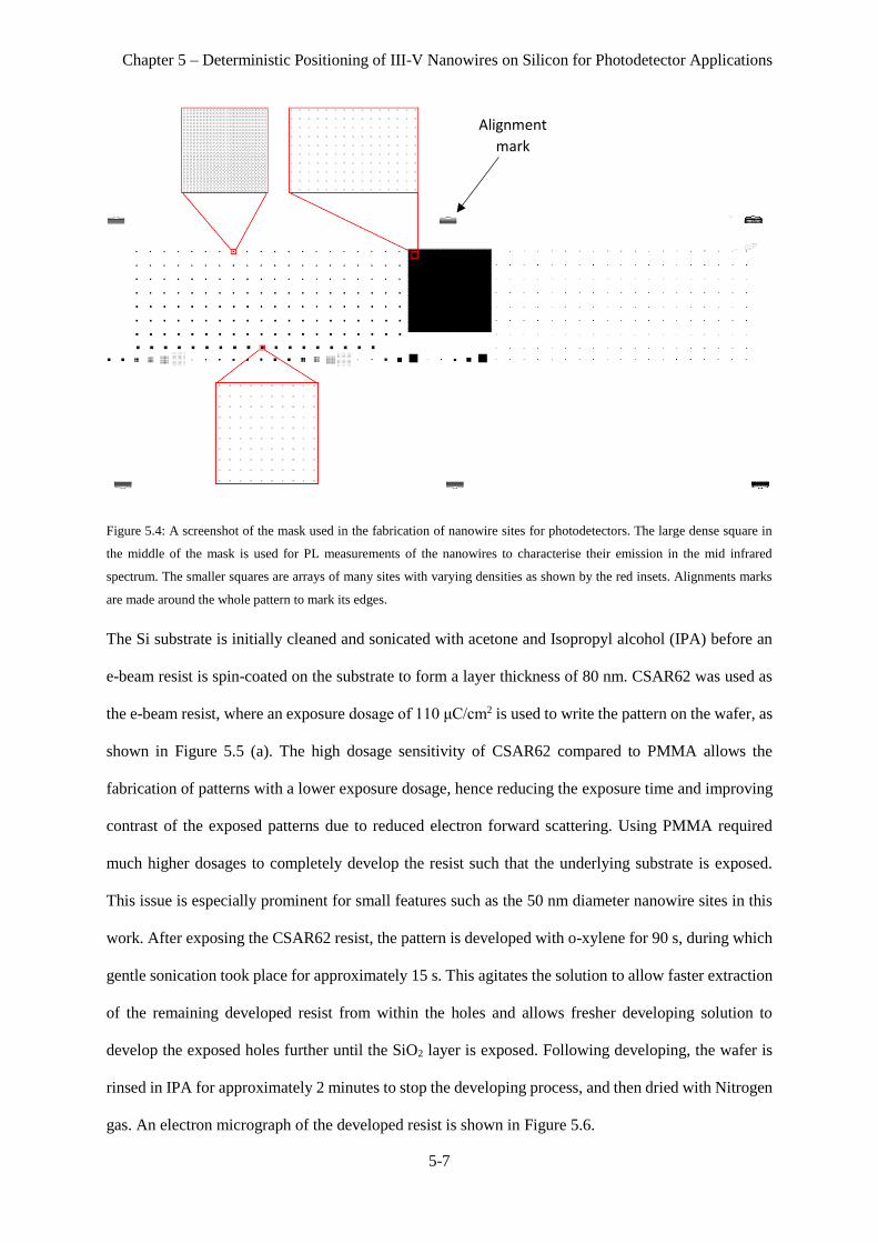
Chapter 5 – Deterministic Positioning of III-V Nanowires on Silicon for Photodetector Applications
5-7
Figure 5.4: A screenshot of the mask used in the fabrication of nanowire sites for photodetectors. The large dense square in
the middle of the mask is used for PL measurements of the nanowires to characterise their emission in the mid infrared
spectrum. The smaller squares are arrays of many sites with varying densities as shown by the red insets. Alignments marks
are made around the whole pattern to mark its edges.
The Si substrate is initially cleaned and sonicated with acetone and Isopropyl alcohol (IPA) before an
e-beam resist is spin-coated on the substrate to form a layer thickness of 80 nm. CSAR62 was used as
the e-beam resist, where an exposure dosage of 110 μC/cm2 is used to write the pattern on the wafer, as
shown in Figure 5.5 (a). The high dosage sensitivity of CSAR62 compared to PMMA allows the
fabrication of patterns with a lower exposure dosage, hence reducing the exposure time and improving
contrast of the exposed patterns due to reduced electron forward scattering. Using PMMA required
much higher dosages to completely develop the resist such that the underlying substrate is exposed.
This issue is especially prominent for small features such as the 50 nm diameter nanowire sites in this
work. After exposing the CSAR62 resist, the pattern is developed with o-xylene for 90 s, during which
gentle sonication took place for approximately 15 s. This agitates the solution to allow faster extraction
of the remaining developed resist from within the holes and allows fresher developing solution to
develop the exposed holes further until the SiO2 layer is exposed. Following developing, the wafer is
rinsed in IPA for approximately 2 minutes to stop the developing process, and then dried with Nitrogen
gas. An electron micrograph of the developed resist is shown in Figure 5.6.
Alignment
mark

Chapter 5 – Deterministic Positioning of III-V Nanowires on Silicon for Photodetector Applications
5-8
The SiO2 layer was wet-etched using a buffered oxide etcher (BOE) (NH4F (35%), H2O (60%) and HF
(5%)) for 40 s. The pattern is then rinsed in deionised water for 60 s and inspected under an optical
microscope. This exact etching process was previously made by Thompson et al in the exact same
conditions20. The work has involved AFM imaging of the etched nanowire sites to ensure that the holes
have etched completely through the oxide layer exposing the Si substrate. After the BOE etching,
CSAR62 did not show any thickness reduction or display signs of removal, this means a high etching
selectivity of over 10:1 can be achieved using CSAR62 as a resist. This is in contrast with PMMA
which normally has an etching selectivity of less than 2:1 with SiO2. The resist is then stripped off from
the substrate using acetone for 5 minutes before being rinsed with IPA for 2 minutes. The pattern
normally appears faint due to the thin SiO2 layer and its transparent nature. Immediately before loading
into the MBE system, the pattern is etched with BOE for 10 s to remove any oxidation due to exposure
to air that might have taken place during the resist strip off or microscope inspection stages. Wet etching
the pattern was found to increase the holes’ diameters to about 90 nm. This is likely to be due to
undercutting of the etched holes which is a normal effect that takes place with chemical wet etching as
shown in Figure 5.7. To solve this issue, it is possible to utilise plasma methods to dry etch the pattern
using reactive ion etching. Using CSAR62 is particularly easier than PMMA in this case due to its
higher etching selectivity. In this work, wet etching was the only method used in all the etching attempts.
Figure 5.5: Illustrations of the steps to fabricate hole sites for nanowire growth on SiO2. (a) Positive CSAR62 e-beam resist is
spin-coated on the substrate. (b) Holes are created by exposing the resist with an e-beam and developing using o-xylene. (c)
The SiO2 layer is etched using buffered oxide etcher, however this causes undercutting in the oxide layer (d) the resist is
stripped off with acetone.
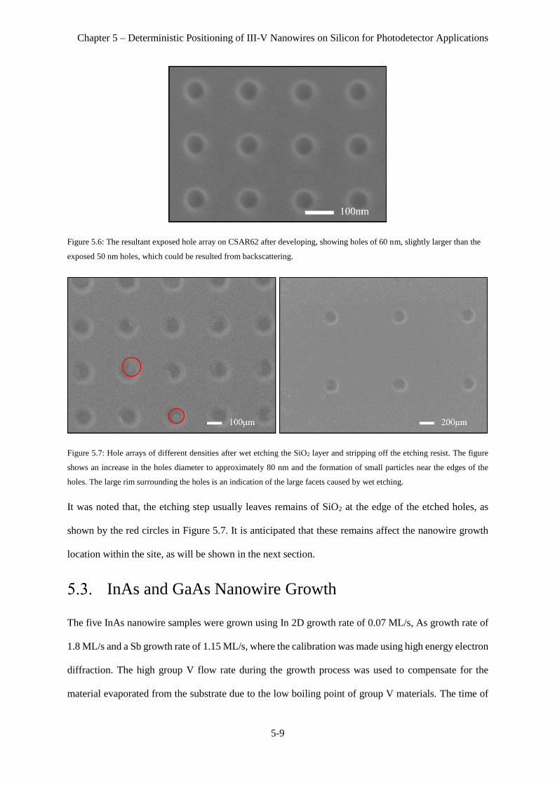
Chapter 5 – Deterministic Positioning of III-V Nanowires on Silicon for Photodetector Applications
5-9
Figure 5.6: The resultant exposed hole array on CSAR62 after developing, showing holes of 60 nm, slightly larger than the
exposed 50 nm holes, which could be resulted from backscattering.
Figure 5.7: Hole arrays of different densities after wet etching the SiO2 layer and stripping off the etching resist. The figure
shows an increase in the holes diameter to approximately 80 nm and the formation of small particles near the edges of the
holes. The large rim surrounding the holes is an indication of the large facets caused by wet etching.
It was noted that, the etching step usually leaves remains of SiO2 at the edge of the etched holes, as
shown by the red circles in Figure 5.7. It is anticipated that these remains affect the nanowire growth
location within the site, as will be shown in the next section.
InAs and GaAs Nanowire Growth
The five InAs nanowire samples were grown using In 2D growth rate of 0.07 ML/s, As growth rate of
1.8 ML/s and a Sb growth rate of 1.15 ML/s, where the calibration was made using high energy electron
diffraction. The high group V flow rate during the growth process was used to compensate for the
material evaporated from the substrate due to the low boiling point of group V materials. The time of

Chapter 5 – Deterministic Positioning of III-V Nanowires on Silicon for Photodetector Applications
5-10
growth was fixed to 1 hour and 20 minutes. After loading the wafer in the MBE growth chamber, it was
annealed at an MBE set point temperature of 700 ºC (corresponding to an actual temperature of 588 ºC,
approximated using the oxide desorption temperature of a n-doped GaAs substrate and the GaAs growth
transition temperature) for 10 minutes before it is allowed to cool down and remain at a constant set
point temperature of 560 ºC (494 ºC actual) for growth. The aim of this is to remove any native oxide
(expected to be around 1 nm thick) that had formed on the opening areas of the masked substrate when
transferring the samples into the MBE chamber. In addition, this step helps removing any other
contaminants and moisture from the substrate surface. The growth is initiated by opening the respective
shutters for the different materials. Once the III-V material reaches the substrate, it diffuses across the
SiO2 until it preferentially bonds to the exposed Si substrate where the nanowire sites have been
fabricated. This is due to its monocrystalline structure relative to the thermally grown SiO2.
The InAs nanowire growth was optimised by only adjusting the wafer’s temperature during the growth
process. It was found that the optimum growth rate for the nanowires was achieved in a small
temperature window. Nanowires of only a few hundred nanometres would require thinner resists for
contacts to be fabricated, which is challenging using UV lithography. On the other hand, long nanowires
of a few microns that enable simpler fabrication, requiring much thicker resists, but this length reduces
light confinement in the vertical direction and causes waveguide losses. The first growth attempt
(sample number 601) was completed by growing the InAs nanowires with a substrate temperature of
560 ºC, with the corresponding results is shown in Figure 5.8. It is easy to observe that the grown
nanowires are relatively short. The lengths of 50 nanowires were measured from the micrograph and a
histogram of the achieved lengths is shown in Figure 5.13. The measured data shows a mean length of
0.31 μm, while the maximum and minimum recorded lengths are 0.43 μm and 0.18 μm respectively.
The short mean length is expected to be attributed to a reduction in the diffusion length of the III-V
atoms on the substrate caused by the low substrate temperature, which reduces the formation of long
nanowires. The micrographs show nanoparticles of InAs seeding throughout the whole substrate
including on the SiO2 layer. Reducing the substrate temperature might increase the chance of seeding

Chapter 5 – Deterministic Positioning of III-V Nanowires on Silicon for Photodetector Applications
5-11
of deposited atoms on the SiO2 layer which would otherwise not bond if their kinetic energy is higher
at higher wafer temperatures.
By increasing the wafer’s growth temperature to 570 ºC (501 ºC actual), longer nanowires were grown
using a similar growth procedure (sample number 576), with a large reduction in seeding of
nanoparticles on non-patterned regions of SiO2, see Figure 5.9. This is a clear indication that the
nanoparticles formed on the surface, as shown in Figure 5.8, are constituted of the growth material
rather than being external contaminants or deformation of the SiO2 layer into nanoparticles shaped
structures. The lengths of 50 nanowires were similarly measured using image analysis techniques. The
blue histogram shown in Figure 5.13 shows the lengths distribution of the nanowires. The mean is
measured to be 0.98 μm, with the maximum and minimum length recorded as 1.65 μm and 0.39 μm
respectively. In comparison with previous results, this length range allows easier contact fabrication for
biasing nanowire based photodetectors. A second attempt was made to repeat the nanowire growth
results achieved at 570 ºC. It can be seen from Figure 5.10 that the nanowire growth takes the square
array pattern of the etched SiO2 hole nanowire sites. The micrograph shows that the achieved growth
success of the nanowires can be over 70%. From Figure 5.13, the centre of the distribution was found
to be approximately 0.87 μm, with maximum and minimum recorded lengths of 1.22 μm and 0.34 μm
respectively. The larger nanowire lengths achieved at higher temperatures is a result of the higher
migration mobility of indium atoms over the substrate before bonding to a nanowire. Arsenic is not
expected to migrate in a similar way to In, but desorb from the substrate without bonding to it. This is
the reason that higher flow rates were used for arsenic in comparison to In. The same applies with
growing GaAs nanowires as will be shown later. This should change when the wires are grown on a
much less dense pattern. It is clear to see that the oxide disrupts the nucleation process of III-Vs at 570
ºC, this is proved by the lack of any seeding on the non-patterned regions. This is in contrast to Si,
which can form strong bonding, particularly with group III atoms.
Attempts were also made to grow nanowires at higher temperatures. Increasing the wafer growth
temperature to 580 ºC and 590 ºC (501 ºC and 516 ºC actual temperatures respectively) was found to
allow clean seeding in the hole sites, however, thermal desorption of As from the silicon substrate reduce

Chapter 5 – Deterministic Positioning of III-V Nanowires on Silicon for Photodetector Applications
5-12
Figure 5.8: Micrograph results from MBE growth of InAs nanowires with a substrate temperature of 560 ºC, grown for 1 hour
and 20 minutes, showing short nanowires (red circles) and large InAs particles forming throughout the substrate.
Figure 5.9: (a) A tilted micrograph image at 70º showing results from MBE growth of InAs nanowires with a substrate
temperature of 570 ºC grown for 1 hour and 20 minutes, showing nanowire lengths closer to the desired value of approximately
1 µm with fewer scattered nanoparticles (b) top view showing the formation of nanowires and nanoparticles on the square
array of nanowires sites. The bright spots represent nanowires while darker spots represent vacant sites.
Figure 5.10: A second of InAs nanowires sample grown using a similar substrate growth temperature of 570 ºC to the sample
shown in the Figure 5.9 and grown in the same system, by Thompson et al. from reference 20. (a) A tilted image at 30º,
showing nanowire formations with lengths over 1 μm. (b) Top view image of the square array of nanowires showing the high
growth ratio of nanowires on the patterned sites, shown as bright dots.

Chapter 5 – Deterministic Positioning of III-V Nanowires on Silicon for Photodetector Applications
5-13
Figure 5.11: Micrograph results from an attempt to grow InAs nanowires at 580 ºC for 1 hour and 20 minutes. The figure
shows the failure of nanowires formation, and the presence of Indium nanoparticles formed in the nanowire sites with a very
clean substrate surface in unpatterned regions. The high temperature is likely to have largely reduced random seeding on
unpatterned SiO2 regions.
Figure 5.12: Micrograph images from an attempt to grow InAs nanowires at 590 ºC showing similar cluster formation resulted
in from growing at 580 ºC, the growth duration was remained constant for 1 hour and 20 minutes.
the abundance of the material on the surface which causes failure in the formation of the nanowires, see
Figures 5.11 and 5.12. The high temperature also reduces the In-SiO2 bonding strength leading to almost
no formation of nanowires on the un-patterned oxide regions, in comparison to small diffusion lengths
of Ga atoms above the substrate at low growth temperatures.
Interestingly, it can be observed from Figure 5.9 (b) that the bright spots of the square array represent
the successful growth of vertical nanowires, while the relatively darker spots are the unsuccessful
formation of nanowires and the formation of nanoparticles. The physical reason behind the brightness
difference between the two can be explained by the regular arrangement of the crystal in the nanowires,

Chapter 5 – Deterministic Positioning of III-V Nanowires on Silicon for Photodetector Applications
5-14
which reflects more electrons than the irregular crystal arrangement of the nanoparticles. This irregular
crystal arrangement makes them exhibit random shapes. Figure 5.14 (a-c) show close up views of the
seeded nanowires in the holes with diameters of 300 nm. Almost all the nanowires were found to seed
and grow near the circumferences of the holes, which is likely to take place over the remains of SiO2
that appear after wet etching as was previously shown in Figure 5.7.
Furthermore, two nanowires can occasionally grow within a single hole when the diameter is large
enough, this can be seen in Figure 5.14 (c). From analysing electron micrographs, the length of the
grown nanowires is found to be dependent on the spatial density of the holes, the difference can be
noted by comparing Figure 5.14 (a-c) with Figure 5.14 (d) and/or Figure 5.15 (a). Longer nanowires
were found to grow as the density of the array of holes was decreased. This is due to the proximity
effect where the largely spaced nanowires collect a greater fraction of precursor material diffused from
larger surrounding areas of the substrate26,27. When the fabricated sites have a high spatial density,
materials that migrate from the surrounding areas are shared with a larger number of sites, hence
reducing the nanowire length per site. The hexagonal shape of the grown nanowires is evident, as shown
in Figure 5.15 (b) and Figure 5.16. However, the hexagonal shape symmetry is not preserved for all the
nanowires throughout the substrate, it is expected that this is due to different growth rates of the different
facets, which is likely to be related to the shape of the nucleation centre.
Hexagonal GaAs nanowires, sample QA618, were grown in a similar fashion on Si with a substrate
growth temperature of 750 ºC (corresponding to 631 ºC actual temperature, approximated using the
oxide desorption temperature of a n-type GaAs substrate and the GaAs transition growth temperature),
following the method proposed by Trukhin et al28. Previous studies have also reported growth of GaAs
nanowires using other methods such as nanoimprint lithography, e-beam lithography and lithography
free techniques29-31. The reported growth temperatures and rates parameters are close to our used
parameters, except the longer time duration which was grown in this work, which produced longer
wires. The aim for realising long nanowires is made primarily for easy fabrication of nanowire-based
photodetectors in the future. The higher band gap of GaAs allows photodetection at smaller
wavelengths, closer to the visible range. The same mask that was used previously in growing InAs

Chapter 5 – Deterministic Positioning of III-V Nanowires on Silicon for Photodetector Applications
5-15
nanowires, was used for fabricating sites for GaAs nanowires. The lengths of the grown nanowires were
found to be larger than those for the previously grown InAs nanowires, for example the red circled
nanowire shown in Figure 5.17 (a) has a length of approximately 4.85 μm compared to 1 μm for the
one in Figure 5.9. Proximity effects were also influential on the nanowires length, for example, the
nanowire shown in Figure 5.18 has a length of approximately 4.85 µm, longer than those shown in
Figure 5.17 (b) that have a length of 4.22 µm. This is due to the lower
Figure 5.13: Length distribution of approximately 50 InAs nanowires measured from the samples in Figure 5.8 (red chart),
Figure 5.9 (blue chart) and Figure 5.10 (green chart) respectively. The mean length of the nanowires from each sample was
found to be approximately 0.31 μm, 0.98 μm and 0.87 μm. The growth of short wires is mainly due to low growth wafer
temperature.
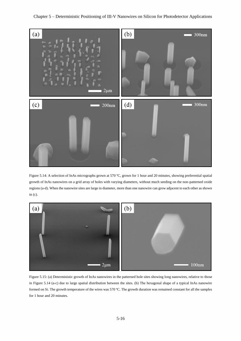
Chapter 5 – Deterministic Positioning of III-V Nanowires on Silicon for Photodetector Applications
5-16
Figure 5.14: A selection of InAs micrographs grown at 570 ºC, grown for 1 hour and 20 minutes, showing preferential spatial
growth of InAs nanowires on a grid array of holes with varying diameters, without much seeding on the non-patterned oxide
regions (a-d). When the nanowire sites are large in diameter, more than one nanowire can grow adjacent to each other as shown
in (c).
Figure 5.15: (a) Deterministic growth of InAs nanowires in the patterned hole sites showing long nanowires, relative to those
in Figure 5.14 (a-c) due to large spatial distribution between the sites. (b) The hexagonal shape of a typical InAs nanowire
formed on Si. The growth temperature of the wires was 570 ºC. The growth duration was remained constant for all the samples
for 1 hour and 20 minutes.

Chapter 5 – Deterministic Positioning of III-V Nanowires on Silicon for Photodetector Applications
5-17
Figure 5.16: Growth results of InAs nanowires grown at 570 ºC for 1 hour and 20 minutes, showing over 60% growth ratio in
the fabricated sites square array. The figures show that the grown nanowires exhibit varying hexagonal geometries.
Figure 5.17: (a) Growth results of the QA618 GaAs nanowires sample showing a 10×10 square array of hole sites separated
by 5μm. (b) Growth results of GaAs nanowires grown on a 10×10 square array of holes sites separated by 1μm. The figure
shows the difference in the grown nanowires lengths for the two arrays due to the different arrays densities.
Figure 5.18: A close up view of a single GaAs (sample QA618) nanowire with a length of 4.85 µm showing cylindrical
formation of nanowires for GaAs in comparison to the previously shown hexagonal nanowires for InAs.
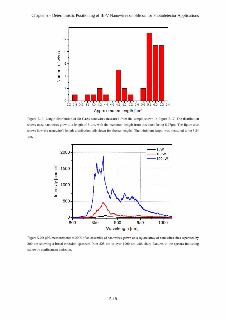
Chapter 5 – Deterministic Positioning of III-V Nanowires on Silicon for Photodetector Applications
5-18
Figure 5.19: Length distribution of 50 GaAs nanowires measured from the sample shown in Figure 5.17. The distribution
shows most nanowires grew to a length of 6 µm, with the maximum length from this batch being 6.27µm. The figure also
shows how the nanowire’s length distribution tails down for shorter lengths. The minimum length was measured to be 3.24
µm.
Figure 5.20: μPL measurements at 20 K of an ensemble of nanowires grown on a square array of nanowires sites separated by
300 nm showing a broad emission spectrum from 825 nm to over 1000 nm with sharp features in the spectra indicating
nanowire confinement emission.

Chapter 5 – Deterministic Positioning of III-V Nanowires on Silicon for Photodetector Applications
5-19
Figure 5.21: μPL measurement spectrum of an individual GaAs nanowire taken at 20 K. The spectrum shows a sharp spike
from a single nanowire, possibly due to an impurity or defect in the lattice. The single nanowire shown here is grown in an
array of sites fabricated with a separation of 5 μm. The large separation is made to ensure exciting only a single nanowire with
the 1 μm laser spot size in the μ-PL setup.
spatial density of the nanowires sites, making each site share larger amount of material with nearby
neighbouring sites in comparison to lower density arrays. Figure 5.19 shows a histogram for 50 GaAs
nanowires measured from different micrographs. It is easy to observe that much larger lengths were
achieved using GaAs at a similar growth temperature. The largest portion of the nanowires were found
to have lengths between 5.60 μm and 6.30 μm, where 6.30 µm was also the maximum length. From this
histogram, it can be seen that shorter nanowires can be found, with the smallest recorded one being 3.24
μm. It was also noted that the growth of GaAs nanowires was not always vertical. A large proportion
of the nanowires were found to be grown slanted at a sharp angle relative to the substrate. Interestingly,
by analysing the figures, the angle distribution was found to be small, which could mean that this angle
is related to the crystal’s facet orientation, making the nanowire’s grow at an angle, in this case aligned
with the (111) plane.
Preliminary micro-photoluminescence measurements were carried out for both an ensemble of GaAs
nanowires and individual ones at 20 K, as a first step toward fabricating p-i-n structures for
photodetection applications. The central emission peak obtained from the ensemble’s μ-PL
measurement show a central emission peak at approximately 868 nm as shown in Figure 5.20. The
central wavelength of the main peak corresponds to the bandgap of GaAs. A long tail for the central
Chapter 5 – Deterministic Positioning of III-V Nanowires on Silicon for Photodetector Applications
5-20
peak was also found to extend to 1 μm. Power dependence measurements on a nanowire ensemble have
shown red shifting in the central emission wavelength for the peak as the power is reduced. Growing
nanowires in a largely spaced grid allows μ-PL of individual nanowires to study their confinement
characteristics. The μ-PL spectrum of the nanowire circled in Figure 5.17 (a) is shown in Figure 5.21.
The spectrum shows a sharp spike with a full width half maximum of 0.8 nm at 851 nm, which could
correspond to quantum-confined states in the nanowire.
Realisation of photodetectors using InAs-based p-i-n structures has been performed recently and is
shown in reference 20. Presently, work is being carried out toward growing similar p-i-n structures in
GaAs for detecting lower wavelengths. Following this, fabrication of front and back gold contacts on
the free-standing nanowires will be carried out.
Conclusion
In summary, the work done in this chapter involved investigating a potential technique of enhancing
single photon detection using nanowire based photodetectors. Results from site-controlled catalyst-free
growth of III-V (InAs and GaAs) nanowires on Si substrates is shown and discussed. To selectively
grow nanowires spatially, e-beam lithography of nanowire hole sites was carried out to preferentially
grow nanowire arrays on a predefined area. The growth of III-V nanowires in this chapter was done on
a p-type Si substrate, solving a huge challenge in the integration of III-V optoelectronic technology on
the common Si platform. InAs and GaAs nanowires for mid- and near-infrared operating wavelengths
were subsequently grown on the fabricated sites. Results show that the growth temperature is vital for
optimum growth of InAs nanowires. Growing at lower temperatures may lead to the formation of short
nanowires due to reduced diffusion length of deposited atoms on the substrate while growing at higher
temperatures may reduce the abundance of V material due to its lower evaporation temperature. Initial
micro-photoluminescence measurements show sharp signatures from an ensemble of nanowires as well
as individual ones.

Chapter 5 – Deterministic Positioning of III-V Nanowires on Silicon for Photodetector Applications
5-21
Bibliography
1 W. T. Tsang. Semiconductors and semimetals. Part D photodetectors. Academic Press, ISBN 978-0-
12-752153-4 (1985)
2 J. C. Campbell. Recent advances in telecommunications avalanche photodiodes. Journal of Lightwave
Technology, 25, 109-121 (2007)
3 N. Han, F. Y. Wang, J. J. Hou, S. P. Yip, H. Lin, F. Xiu, M. Fang, Z. X. Yang, X. L. Shi, G. F. Dong,
T. F. Hung, J. C. Ho. Tunable electronic transport properties of metal-cluster-decorated III-V nanowire
transistors. Advanced Materials Communication, 25, 4445-4451 (2013)
4 T. Takahashi, K. Takei, E. Adabi, Z. Y. Fan, A. M. Niknejad, A. Javey. Parallel array InAs nanowire
transistors for mechanically bendable, ultrahigh frequency electronics. ACS Nano, 4, 5855-5860 (2010)
5 A. C. Ford, J. C. Ho, Y. L. Chueh, Y. C. Tseng, Z. Y. Fan, J. Guo, J. Bokor, A. Javey. Diameter-
dependent electron mobility of InAs nanowires. Nano Lett., 9, 360-365 (2009)
6 M. S. Gudikssen, L. K. Lauhon, J. F. Wang, D. C. Smith, C. M. Lieber. Growth of nanowire
superlattice structures for nanoscale photonics and electronics. Nature, 415, 617-620 (2002)
7 Y. J. Dong, B. Z. Tian, T. J. Kempa, C. M. Lieber. Coaxial group III-nitride nanowire photovoltaics.
Nano Lett., 9, 2183-2186 (2009)
8 C. Thelander, L. E. Froberg, C. Rehnstedt, K. Samuelson, L. E. Wernersson. Vertical enhancement-
mode InAs nanowire field-effect transistor with 50-nm wrap gate. IEEE Electronic Device Lett., 29-
206-208 (2008)
9 H. Xia, Z. Y. Lu, T. X. Li, P. Parkinson, Z. M. Liao, F. H. Liu, W. Lu, W. D. Hu, P. P. Chen, H. Y.
Xu, J. Zou, C. Jagadish. Distinct photocurrent response of individual GaAs nanowires induced by n-
type doping. ACS Nano, 6, 6005-6013 (2012)
10 R. E. Wahl, F. Y. Wang, H. E. Chung, G. R. Kunnen, S. P. Yip, E. H. Lee, E. Y. B. Pun, G. B. Raupp,
D. R. Allee, J. C. Ho. Stability and low-frequency noise in InAs NW parallel array thin-film transistors.
IEEE Electron Device Lett., 34, 765-767 (2013)
11 L. Rogalski. Infrared detectors: status and trends. Prog. Quant. Electron., 27, 59-210 (2003)
12 L. Becker. Current and future trends in infrared focal plane array technology. Proc. SPIE, 5881,
588105 (2005)
13 T. Martensson, C. P. T. Svensson, B. A. Wacaser, M. W. Larsson, W. Seifert, K. Deppert, A.
Gustafsson, L. R. Wallenberg, L. Samuelson. Epitaxial III-V nanowires on silicon. Nano Lett., 4, 1987-
1990 (2004)
14 M. Paladugu, C. Merckling, R. Loo, O. Richard, H. Bender, J. Dekoster, W. Vandervorst, M. Caymax,
M. Heyns. Site selective integration of III-V materials on Si for nanoscale logic and photonic devices.
Crys. Growth Des., 12, 4696-4702 (2012)
15 R. S. Chen, H. Y. Chen, C. Y. Lu, K. H. Chen, C. P. Chen, L. C. Chen, Y. J. Yang. Ultrahigh
photocurrent gain in m-axial GaN nanowires. Appl. Phys. Lett., 91, 223106 (2007)
Chapter 5 – Deterministic Positioning of III-V Nanowires on Silicon for Photodetector Applications
5-22
16 J. Miao, W. Hu, N. Guo, Z. Lu, X. Zou, L. Liao, S. Shi, P. Chen, Z. Fan, J. C. Ho, T. Li, X. S. Chen,
W. Lu. Single InAs nanowire room-temperature near infrared photodetectors. ACS Nano, 8, 3628-3635
(2014)
17 H. W. Shin, S. J. Lee, D. G. Kim, M. Bae, J. Heo, K. J. Choi, W. J. Choi, J. Choe, J. C. Shin. Short-
wavelength infrared photodetector on Si employing strain-induced growth of very tall InAs nanowire
arrays. Sci. Rep., 5, 10764 (2015)
18 E. M. Gallo, G. N. Chen, M. Currie, T. McGuckin, P. Prete, N. Lovergine, B. Nabet, J. E. Spainer.
Picosecond response times in GaAs/AlGaAs core/shell nanowire-based photodetectors. Appl. Phys.
Lett., 98, 241113 (2011)
19 X. C. Jiang, Q. H. Xiong, S. Nam, F. Qian, Y. Li, C. M. Lieber. InAs/InP radial nanowire
heterostructures as high electron mobility devices. Nano Lett., 7, 3214-3218 (2007)
20 M. D. Thompson, A. Alhodaib, A. P. Craig, A. Robson, A. Aziz, A. Krier, J. Svensson, L.
Wernersson, A. M. Sanchez, A. R. J. Marshall. Low leakage-current InAsSb nanowire photodetectors
on silicon. Nano Lett., 16, 182-187 (2016)
21 M. J. L. Sourribes, I. Isakov, M. Panfilova, H. Liu, P. A. Warburton. Mobility enhancement by Sb-
mediated minimisation of stacking fault density in InAs nanowires grown on silicon. Nano Lett., 145,
1643-1650 (2014)
22 M. D. Kelzenberg, D. B. Turner-Evans, B. M. Kayes, M. A. Filler, M. C. Putnam, N. S. Lewis, H. A.
Atwater. Photovoltaics measurements in single-nanowire silicon solar cells. Nano Lett., 8, 710-714
(2008)
23 Y. Cui, Z. Zhong, D. Wang, W. U. Wang, C. M. Lieber. High performance silicon nanowire field
effect transistors. Nano Lett., 3, 149-152 (2003)
24 D. Wang, B. A. Sheriff, J. R. Heath. Silicon P-FETs from ultrahigh density nanowire arrays. Nano
Lett., 6, 1096-1100 (2006)
25 M. D. Kelzenberg, S. W. Boettcher, J. A. Petykiewicz, et al.. Enhanced absorption and carrier
collection in Si wire arrays for photovoltaic applications. Nature Mater., 9, 239-244 (2010)
26 H. J. Joyce, Q. Gao, H. H. Tan, C. Jagadish, Y. Kim, J. Zou, L. M. Smith, H. E. Jackson, J. M.
Yarrison-Rice, P. Parkinson, M. B. Johnston. III-V semiconductor nanowires for optoelectronic device
applications. Progress in Quantum Electronics, 35, 23-75 (2011)
27 M. H. Madsen, M. Aagesen, P. Krogstrup, C. Sørensen, J. Nygård. Influence of the oxide layer for
growth of self-assisted InAs nanowires on Si(111). Nanoscale Res. Lett., 6, 516 (2011)
28 V. N. Trukhin, A. S. Buyskikh, N. A. Kaliteevskaya, A. D. Bourauleuv, L. L. Samoilov, Y. B.
Samsonenko, G. E. Cirlin, M. A. Kaliteevski, A. J. Gallant. Terahertz generation by GaAs nanowires.
Appl. Phys. Lett., 103, 072108 (2013)
29 A. M. Munshi, D. L. Dheeraj, V. T. Fauske, D. C. Kim, J. Huh, J. F. Reinertsen, L. Ahtapodov, K.
D. Lee, B. Heidari, A. T. J. Helvoort, B. O. Fimland, H. Weman. Position-controlled uniform GaAs
nanowires on silicon using nanoimprint lithography. Nano Lett., 14, 960-966 (2014)
30 S. Plissard, G. Larrieu, X. Wallart, P. Caroff. High yield of self-catalyzed GaAs nanowire arrays
grown on silicon via gallium droplet positioning. Nanotechnology, 22, 275602 (2011)

Chapter 5 – Deterministic Positioning of III-V Nanowires on Silicon for Photodetector Applications
5-23
31 E. Koivusalo, T. Hakkarainen, M. Guina. Structural investigation of uniform ensembles of self-
catalyzed GaAs nanowires fabricated by lithography-free technique. Nanoscale Research Letters,
12:192 (2017)

Chapter 6 – A Quantum Key Distribution Chip Design
6-1
Chapter 6
A Quantum Key Distribution Chip Design
Introduction
QKD has recently attracted great research attention for the potential it offers in securing everyday digital
communications1-3. In the present day, the largest obstacle that prevents QKD systems from inhabiting
many consumer grade electronics is their large size and cost. This makes QKD used solely by
organisations, banks and governments that have large financial resources. This chapter will introduce a
design that is aimed at miniaturizing QKD systems to the chip level, thereby paving the way towards
integrating QKD in handheld devices and embedded systems for securing their communications.
In this chapter, current research into integrated optical components, such as cavities, waveguides and
out-couplers will be introduced. A discussion will follow to compare the different types of integrated
optical components, and the most practical of these will be used for proposing a full system. Numerical
simulations of these components and design optimisations will be performed to improve many of their
aspects, such as increasing their coupling efficiencies and reducing their losses. Finally, a full QKD
system made of the optimised optical components will be presented as a strong candidate for future
integrated QKD systems.

Chapter 6 – A Quantum Key Distribution Chip Design
6-2
6.1.1. Motivation
Secure key sharing with QKD was explained in chapter 1 using the polarisation degree of freedom for
encoding quantum information on photons4. However, these qubits can also be encoded with the phase
difference between successive photons pulses. Realising a QKD system by encoding 1s and 0s on the
phase difference between photon pulses is known as Differential Phase Shift (DPS) QKD5. Practically,
DPS-QKD is much less susceptible to environmental fluctuations, relative to polarisation encoding. In
addition, while integrated polarisation rotators have been introduced before, integrated phase
modulators have been extensively studied and have shown great promise for optical digital
communications6-8.
Figure 6.1: A block diagram of a double Mach-Zehnder interferometer DPS-QKD system. Successive pulses from the single
photon source (component A) on Alice’s side are phase modulated (using component C) and interfered before being out-
coupled (using component D) from the chip. Bob performs similar interferometric measurements using a similar setup
(Components BCB). Interfered photons are then recorded by detectors 1 or 0, depending on their phase difference.
A state-of-the-art integrated DPS-QKD system was demonstrated by Sibson et al9. The system benefits
from the already established Si optoelectronic technology, using an attenuated laser source that operates
at telecom wavelengths. However, since QKD is prone to the photon number splitting attacks when a
Poisson source is used, the average number of photons per pulse is largely reduced, hence reducing the
achievable bit rate10. This makes an alternative method that involves a high bit rate, integrated source
of indistinguishable photons necessary for fast and perfectly secure QKD systems. In addition, the QKD
system demonstrated in reference 9 requires the complicated growth of structures with multiple
lithography processes to realise the full system including the laser source, the waveguides and the phase
modulator. In this thesis, a much simpler system that requires less complicated growth structures that
can be fabricated with a single lithography process based on PhCs will be suggested. Using a PhC

Chapter 6 – A Quantum Key Distribution Chip Design
6-3
platform based on GaAs, shorter phase modulators can be fabricated leading to further miniaturization
of the technology.
The different components A, B, C and D shown in Figure 6.1 that are being used as parts of a typical
DPS-QKD system will be introduced and discussed. PhC cavities will be suggested and optimised as a
potential platform for realising single photon sources. For part B of the system, a new beam splitting
scheme in which light couples to two waveguides following emission from the cavity will be simulated
and the cavity-waveguide coupling efficiency will be enhanced for reducing losses. Different methods
in realising part C of the system will be discussed. Finally, as part of improving part D of the system,
current techniques for light out-coupling will be explained and numerical modelling will be performed
for optimised coupling between a PhC waveguide and a Bragg mirror out-coupler.
6.1.2. GaAs as an Optoelectronic Material for QKD
One of the most critical components in a secure QKD system is a pure single photon source10. Many of
the requirements of an ideal single photon source are discussed in chapter 4. While ideal single photon
sources are still far from being commercially available, InAs quantum dots (QDs) are one of the most
promising sources of single photons11. The drawback that InAs QDs suffer from which makes them
impractical for commercial applications is their operation temperature. However, research into single
photon sources based on InAs for quantum information applications has shown that such systems have
many advantages over others, including the operation wavelength, photon indistinguishability, short
lifetime and compatibility with optoelectronics materials such as GaAs12,13. These advantages are the
main driving motivation towards achieving a secure GaAs chip-based QKD system.
There has been a great debate over the years about which is the most ideal material for optoelectronic
applications. The top two that were debated for were Silicon and Gallium Arsenide. Compared to GaAs,
Silicon is one of the most abundant materials on earth and compatible with current industrial device
fabrication processing. In terms of its optical properties, Si’s indirect bandgap means it is an inefficient
light absorber and emitter and renders it of little use in most optoelectronic applications. On the other
hand, the direct bandgap of GaAs and InP means they emit and absorb light efficiently at different
wavelengths14. In contrast to InP, GaAs has been studied extensively and has a lattice match with alloys

Chapter 6 – A Quantum Key Distribution Chip Design
6-4
such as AlGaAs and Al2O3 that are widely involved in many GaAs-based optoelectronic applications
for creating tunnel barriers, laser diodes and photodetector heterostructures.
For integrated optical components, it is desirable to operate at a wavelength where there is minimum
absorption. Due to GaAs’s direct bandgap, its absorption reduces to virtually zero at wavelengths above
870 nm, while Silicon absorption is two orders of magnitudes higher at that wavelength. It is known
that the wavelength emission range of InAs QDs is centred at 915 nm and spans a width of
approximately 60 nm. Figure 6.2 show a typical spectrum obtained from self-assembled InAs QDs at
20 K. In addition, operating in this wavelength range makes QKD systems compatible with the
commercially available single photon detectors that normally have maximum quantum efficiency in
this range15. Finally, the property that both GaAs and InAs possess is that they are a III-V
semiconductor, this makes GaAs an ideal environment material for the epitaxial growth of InAs QDs
due to matching structural lattices. Hence, fabricating an integrated QKD chip that harnesses the single
photon emission property of InAs should be done on GaAs.
Figure 6.2: A typical micro-photoluminescence spectrum recorded for an InAs QD ensemble at 20 K and 10 μW laser power.
The figure shows clear signatures of sharp emission lines due to the QD exciton confinement with a possible signature of bi-
exciton lines at around 935 nm.
Chapter 6 – A Quantum Key Distribution Chip Design
6-5
Researchers have previously demonstrated single photon emission from InAs QDs capped with GaAs16.
Much of this work was motivated by proposed applications in quantum computing and quantum
communications. Efforts have also been made toward engineering photonic structures such as optical
cavities and waveguides around InAs QDs16, mainly to manipulate the quantum states that emitted
photons carry. As a result, on chip Purcell enhancement in QDs17, single photon guiding and dipole
induced transparency18 have all been reported. This was made possible by the developments of
lithography techniques such as electron-beam (e-beam) lithography and dry etching techniques on
GaAs. Observing the progress and extensive studies being made on InAs QDs using a GaAs substrate
was one of the key motivational forces toward designing a chip-based QKD system. The current aim is
epitaxial integration of all the optical components that assemble a QKD system into a single chip,
preferably including integration of GaAs and other III-V unique optoelectronic materials with
conventional Si technology.
Components for QKD
In this section of the chapter, an introduction to the main components needed for QKD will be given
and current techniques to realise these components will be summarised. A comparison will be made
between the different techniques needed to realise every component and an option will be favoured
based on the goal of achieving a chip-based QKD system.
6.2.1. Single Photon Cavity for QKD
Over the years, different GaAs cavities have been proposed and constructed19. The ultimate aim is to
improve light-matter coupling by confining the light’s electric and magnetic field components inside a
structure where a two-level light emitter exists such as a QD20-22, an atom23,24, a nitrogen vacancy centre
in diamond25, etc. This coupling increases the emitter’s absorption and spontaneous emission rate.

Chapter 6 – A Quantum Key Distribution Chip Design
6-6
Figure 6.3: Schematic illustration of different proposed cavity designs for enhancing the spontaneous emission rate from QDs.
The figure shows a common (a) micro-pillar (b) micro-disc and (c) L3 PhC cavity. The blue flare shown in (a) represents the
direction of light travel, while those in (b) are a visual representation of the whispering gallery mode in the micro-disc.
One design is known as a pillar micro-cavity13. In this cavity, the light is trapped within the vertical
height of a GaAs pillar which has a diameter on the order of one cavity mode wavelength. Along the
vertical height of the cavity, a distributed Bragg mirror is grown epitaxially to trap the light in the active
region of the cavity which includes the quantum emitter. Previous work has shown Purcell enhancement
from coupling an InAs QD situated in the centre of the cavity to the cavity mode13. The number of
Bragg mirror layers grown above the cavity is slightly smaller than below to allow the cavity to
preferentially radiate light modes vertically upward, as shown by the blue flares in Figure 6.3 (a). The
distributed Bragg structure could be considered as a 1D PhC that can confine the light due to the
photonic band in the x-z and y-z planes of the pillar. Light is confined laterally in the x-y plane due to
total internal reflection at the GaAs-air interface of the pillar.
A second type of cavity constitutes another class of resonator where the light is trapped in the x-y plane
due to a Whispering Gallery mode at the rim of a GaAs disk26, as in Figure 6.3 (b). Finally, another
GaAs cavity design is based on a 2D-bridge type PhC, as in Figure 6.3 (c)17. In this type of cavities,
the light is confined in the x-y plane due to the photonic bandgap and confined in the z-plane due to
total internal reflection at the GaAs-air interfaces at the top and bottom. More of the basics of PhCs and
related references can be found in chapter 2.
Each of these cavity types have advantages over the other. In terms of the quality factor, it is known
that whispering gallery modes in a micro-disc are usually higher than those achieved in micro-pillars
and PhC cavities19. The highest Q-factor achieved experimentally in coupling whispering gallery modes
to InAs QDs was reported by Srinivasan et al.19 to be 4 × 10⁵. The highest Q-factors achieved in
Chapter 6 – A Quantum Key Distribution Chip Design
6-7
coupling GaAs bridge-type PhCs and micro-pillar cavities to InAs QDs were reported by Hennessy et
al. and Loo et al. as 3 × 10⁵ and 6 × 10⁴, respectively26-28. Due to the nature of the whispering gallery
mode, the mode volume for micro-disc cavities is usually much higher than those of a bridge-type PhC
and micro-pillar cavities. The latter usually has the smallest achievable mode volume of 1
10(
𝜆
𝑛)
3, while
being on the order of (𝜆
𝑛)
3 and 10 (
𝜆
𝑛)
3for bridge-type PhCs and micro-disc cavities.
Fabrication wise, it is widely known that PhC cavities are more prone to fabrication imperfections
compared to micro-disc and micro-pillar cavities. Surface roughness of the bridge and/or the etching
profile of the fabricated holes can reduce its Q-factor dramatically and affect its mode volume.
Nonetheless, decent results have been reported over the past few years, and the availability of many of
the fabrication tools required make it a routinely achievable challenge.
For QKD applications where photon manipulation and processing is carried out on a chip, coupling
light efficiently from a cavity is critical. Previously, coupling of light from a micro-disc cavity was
carried out using a single mode fibre optic spatially positioned within a few hundred nanometres from
the rim of the micro-disc29. This coupling process requires precise positioning of the fibre optic making
the setup extremely sensitive to vibrations, hence it is unsuitable for mass manufacturing. Meanwhile,
due to light being emitted from a micro-pillar vertically, coupling light back to the chip for processing
using mirrors or a focusing objective is also sensitive to optical alignments and could introduce losses.
Coupling a PhC cavity to a PhC waveguide can be easily achieved by engineering the photonic band
structure of the crystal. PhC cavity-waveguide coupling can be easily simulated and different designs
can be reliably fabricated and tested using e-beam lithography and Inductively Coupled Plasma (ICP)
etching on GaAs30. The decent Q-factors achievable with the medium mode volume and efficient
coupling that PhC cavities can offer makes it an ideal choice for integrated QKD systems.
6.2.2. Integrated Waveguides for QKD
Integrated waveguides for on chip photonic interconnects divide into two common types. The first is a
ridge waveguide in which light is confined in the centre core of the guiding layer due to the index
contrast that surrounds the guiding layer, as shown in Figure 6.4 (a)6,31. Ridge waveguides are more
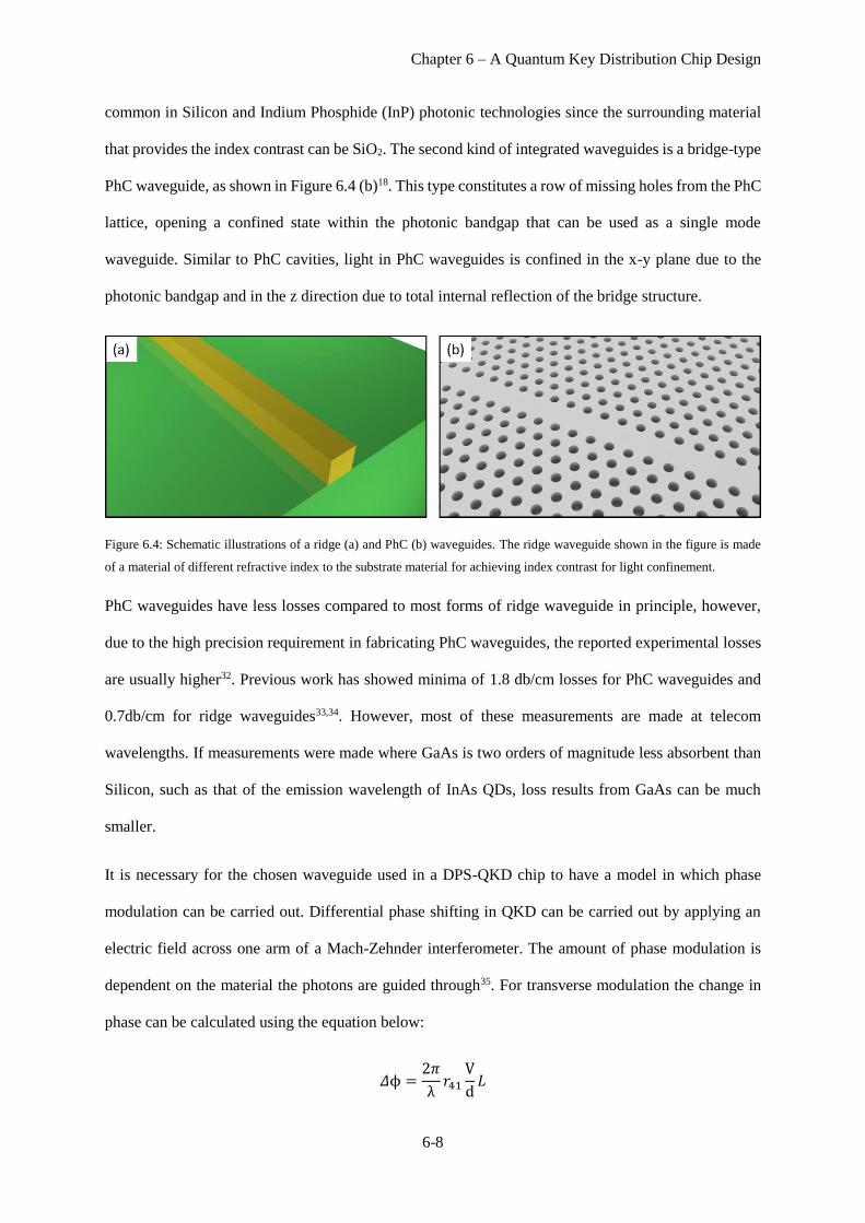
Chapter 6 – A Quantum Key Distribution Chip Design
6-8
common in Silicon and Indium Phosphide (InP) photonic technologies since the surrounding material
that provides the index contrast can be SiO2. The second kind of integrated waveguides is a bridge-type
PhC waveguide, as shown in Figure 6.4 (b)18. This type constitutes a row of missing holes from the PhC
lattice, opening a confined state within the photonic bandgap that can be used as a single mode
waveguide. Similar to PhC cavities, light in PhC waveguides is confined in the x-y plane due to the
photonic bandgap and in the z direction due to total internal reflection of the bridge structure.
Figure 6.4: Schematic illustrations of a ridge (a) and PhC (b) waveguides. The ridge waveguide shown in the figure is made
of a material of different refractive index to the substrate material for achieving index contrast for light confinement.
PhC waveguides have less losses compared to most forms of ridge waveguide in principle, however,
due to the high precision requirement in fabricating PhC waveguides, the reported experimental losses
are usually higher32. Previous work has showed minima of 1.8 db/cm losses for PhC waveguides and
0.7db/cm for ridge waveguides33,34. However, most of these measurements are made at telecom
wavelengths. If measurements were made where GaAs is two orders of magnitude less absorbent than
Silicon, such as that of the emission wavelength of InAs QDs, loss results from GaAs can be much
smaller.
It is necessary for the chosen waveguide used in a DPS-QKD chip to have a model in which phase
modulation can be carried out. Differential phase shifting in QKD can be carried out by applying an
electric field across one arm of a Mach-Zehnder interferometer. The amount of phase modulation is
dependent on the material the photons are guided through35. For transverse modulation the change in
phase can be calculated using the equation below:
𝛥ϕ =2𝜋
λ𝑟41
V
d𝐿

Chapter 6 – A Quantum Key Distribution Chip Design
6-9
where r41 is the 4-1 component of the electro-optic matrix for GaAs, E is the electric field applied across
the waveguide, d and L are the width and length of the waveguide respectively. The same applies for
Silicon, however, different tensor components should be taken into account for different guided modes
(TE or TM) because the electro-optic modulation is different when the electric field is applied at
different orientations.
The waveguide’s length is important here to ensure 𝜋 phase modulations are performed as the photons
travel through the waveguide, without applying high voltages and facing heating issues. Applying a
high voltage per pulse can also be difficult to generate electronically. Furthermore electron tunnelling
and/or arcing might occur in this small length scale. These issues become even more prominent when
operating at high operation frequencies for fast QKD bit rates. Compared to ridge waveguides, PhC
waveguides can play a vital role in reducing the length of the waveguide by harnessing slow light
effects. Reduction in the group velocity of light due to slow light effects can shorten the waveguide by
an order of magnitude while achieving the same phase modulation using similar applied voltages. The
symmetric strong electro-optic modulation and low absorption of GaAs at the InAs emission
wavelength, combined with the slow light effect of PhCs makes the two ideal for integrated phase
modulation.
Recently, researchers have proposed and tested a scheme for PhC phase modulators. In this scheme, p-
i-n doped regions are made across a PhC waveguide to provide a strong electric field for electro-optic
modulation36. The waveguide is fabricated with e-beam lithography, dry and wet etching, and doped
using ion-implantation. It is important to take doping’s effect on the refractive index into account when
designing PhC phase modulators. Changes in the doping between the n and p regions can require
modification to the symmetry of the crystal in the y-direction to compensate for this. To compensate
for the change in index in regions surrounding the waveguide, the photonic crystal lattice may be altered
by modifying the radii of the holes in these regions or modifying their lattice constant.

Chapter 6 – A Quantum Key Distribution Chip Design
6-10
Figure 6.5: The proposed phase modulation scheme used in the QKD system. The schematic shows the different doping regions
needed to allow phase modulation to guided modes in the PhC waveguide.
6.2.3. Photon Out-Coupling for a QKD Chip
Coupling light efficiently out of a chip for carrying out chip to chip communications, for example, is
important for reducing photon losses and increasing key bit rates in a QKD system. There have been a
few different designs suggested for light out-coupling, such as using a Bragg mirror based or tapered
mode out-coupler, as shown in Figure 6.6.
The difference between the Bragg and tapered mode out-couplers is that the first directs light in the
vertical direction out of the chip, while the second can only emit the light in a parallel direction to the
chip. Although practically, it is much easier to collect the light from above the chip using an objective
lens or a lensed fibre aligned above the out-coupler, it is still challenging to perform coupling without
precise alignments, therefore addressing this challenge becomes difficult industrially for consumer
grade devices.
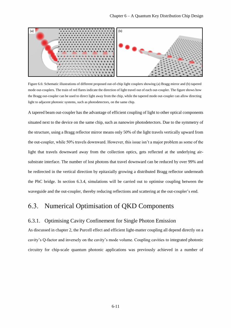
Chapter 6 – A Quantum Key Distribution Chip Design
6-11
Figure 6.6: Schematic illustrations of different proposed out-of-chip light couplers showing (a) Bragg mirror and (b) tapered
mode out-couplers. The train of red flares indicate the direction of light travel out of each out-coupler. The figure shows how
the Bragg out-coupler can be used to direct light away from the chip, while the tapered mode out-coupler can allow directing
light to adjacent photonic systems, such as photodetectors, on the same chip.
A tapered beam out-coupler has the advantage of efficient coupling of light to other optical components
situated next to the device on the same chip, such as nanowire photodetectors. Due to the symmetry of
the structure, using a Bragg reflector mirror means only 50% of the light travels vertically upward from
the out-coupler, while 50% travels downward. However, this issue isn’t a major problem as some of the
light that travels downward away from the collection optics, gets reflected at the underlying air-
substrate interface. The number of lost photons that travel downward can be reduced by over 99% and
be redirected in the vertical direction by epitaxially growing a distributed Bragg reflector underneath
the PhC bridge. In section 6.3.4, simulations will be carried out to optimise coupling between the
waveguide and the out-coupler, thereby reducing reflections and scattering at the out-coupler’s end.
Numerical Optimisation of QKD Components
6.3.1. Optimising Cavity Confinement for Single Photon Emission
As discussed in chapter 2, the Purcell effect and efficient light-matter coupling all depend directly on a
cavity’s Q-factor and inversely on the cavity’s mode volume. Coupling cavities to integrated photonic
circuitry for chip-scale quantum photonic applications was previously achieved in a number of

Chapter 6 – A Quantum Key Distribution Chip Design
6-12
reports16,37. Simple cavities such as the L3, H0 and H1 cavities are widespread designs due to their
simplicity, compactness, high Q-factor and the small mode-volume they have, making them practical
for integrated photonic circuit applications.
In designing a PhC structure for GaAs, it is important to take into account the exact refractive index
that corresponds to the wavelength of interest. For GaAs, the refractive index for the central emission
wavelength of 915 nm in which InAs QDs emit is approximately 3.59.
H0 and H1 have shown large Q-factors and very small mode volumes. Their small mode volume make
them inefficient in waveguide coupling, which is important for an integrated QKD system. In addition,
H0 cavities mode maximum is not centred in the middle of the cavity, in contrast to L3 cavities38. The
larger mode volumes for L3 cavities make them more attractive in such applications. Optimising cavity
Q-factors can cause large Purcell enhancements, hence allowing the realisation of high bitrate single
photon sources.
Optimising the Q-factor for L3 cavities can be done by changing the radii and positions of the nearby
holes surrounding the cavity. These holes will be labelled A to E based on their distance to the cavity.
Figure 6.7: The design of an unmodified L3 cavity, indicating the direction of displacement of holes A-E. The displacement S
is the distance holes A-E moved from their normal position.

Chapter 6 – A Quantum Key Distribution Chip Design
6-13
Figure 6.7 shows these holes and the arrows that indicate the direction of displacement, S, for the holes.
This simple method has been shown to be capable of increasing the cavities Q-factor by orders of
magnitude while maintaining the same mode volume38. Using this technique, a series of simulations
were completed to suggest different improved designs that give high Q-factors from an L3 cavity. The
mode wavelengths will be presented in normalised units of the lattice constant, 𝑎 = 1. For an
explanation of the methods used to perform FDTD simulations of the cavities, see chapter 2.
Figure 6.8: The relationship between changing the radius of holes, A, on the cavity resonant wavelength (a) and the cavity
mode’s volume (b). The figure shows increasing the holes radius causes the cavity mode to blue shift. The Q-factor however,
can fluctuate, hence careful selection of the holes radius is necessary for optimised Q cavities.
Figure 6.9: An x-y cross section of the simulated PhC cavity through the bridge structure. The 3D FDTD simulations of the
photonic cavity mode show time slice images of the confined (a) Ex (b) Ey and (c) Hz field components within the bridge
structure of the cavity. Red (blue) indicate positive (negative) components of the electric field.
Unmodified L3 Cavity
The unmodified L3 cavity is made of three missing holes from the lattice, without any modification in
the positions or radii of holes A-E. A series of simulations were carried out to investigate at which
radius is the maximum Q-factor obtained, before proceeding with performing small modifications to
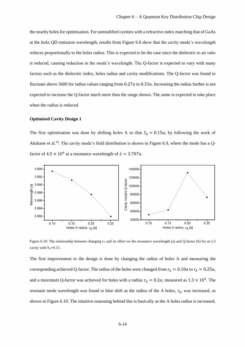
Chapter 6 – A Quantum Key Distribution Chip Design
6-14
the nearby holes for optimisation. For unmodified cavities with a refractive index matching that of GaAs
at the InAs QD emission wavelength, results from Figure 6.8 show that the cavity mode’s wavelength
reduces proportionally to the holes radius. This is expected to be the case since the dielectric to air ratio
is reduced, causing reduction in the mode’s wavelength. The Q-factor is expected to vary with many
factors such as the dielectric index, holes radius and cavity modifications. The Q-factor was found to
fluctuate above 5600 for radius values ranging from 0.27𝑎 to 0.33𝑎. Increasing the radius further is not
expected to increase the Q-factor much more than the range shown. The same is expected to take place
when the radius is reduced.
Optimised Cavity Design 1
The first optimisation was done by shifting holes A so that 𝑆𝐴 = 0.15𝑎, by following the work of
Akahane et al.39. The cavity mode’s field distribution is shown in Figure 6.9, where the mode has a Q-
factor of 4.5 × 10⁴ at a resonance wavelength of 𝜆 = 3.707𝑎.
Figure 6.10: The relationship between changing rA and its effect on the resonance wavelength (a) and Q-factor (b) for an L3
cavity with SA=0.15.
The first improvement to the design is done by changing the radius of holes A and measuring the
corresponding achieved Q-factor. The radius of the holes were changed from 𝑟𝐴 = 0.10𝑎 to 𝑟𝐴 = 0.25𝑎,
and a maximum Q-factor was achieved for holes with a radius 𝑟𝐴 = 0.2𝑎, measured as 1.3 × 10⁵. The
resonant mode wavelength was found to blue shift as the radius of the A holes, 𝑟𝐴, was increased, as
shown in Figure 6.10. The intuitive reasoning behind this is basically as the A holes radius is increased,
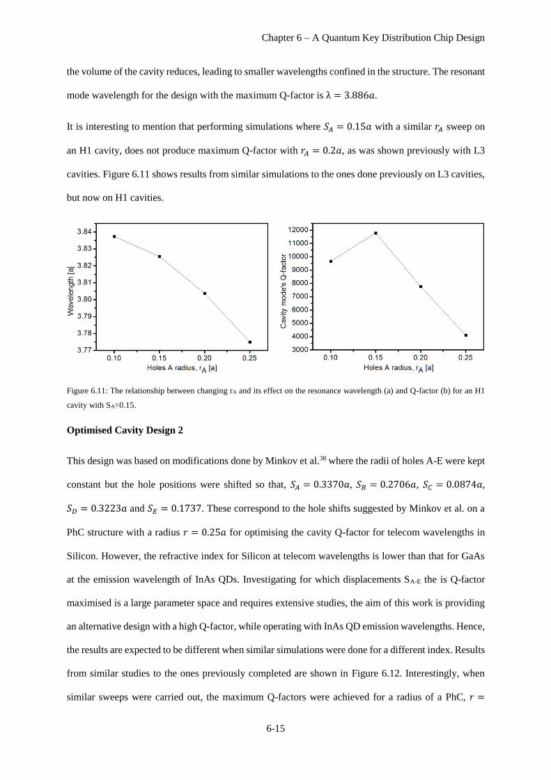
Chapter 6 – A Quantum Key Distribution Chip Design
6-15
the volume of the cavity reduces, leading to smaller wavelengths confined in the structure. The resonant
mode wavelength for the design with the maximum Q-factor is λ = 3.886𝑎.
It is interesting to mention that performing simulations where 𝑆𝐴 = 0.15𝑎 with a similar 𝑟𝐴 sweep on
an H1 cavity, does not produce maximum Q-factor with 𝑟𝐴 = 0.2𝑎, as was shown previously with L3
cavities. Figure 6.11 shows results from similar simulations to the ones done previously on L3 cavities,
but now on H1 cavities.
Figure 6.11: The relationship between changing rA and its effect on the resonance wavelength (a) and Q-factor (b) for an H1
cavity with SA=0.15.
Optimised Cavity Design 2
This design was based on modifications done by Minkov et al.38 where the radii of holes A-E were kept
constant but the hole positions were shifted so that, 𝑆𝐴 = 0.3370𝑎, 𝑆𝐵 = 0.2706𝑎, 𝑆𝐶 = 0.0874𝑎,
𝑆𝐷 = 0.3223𝑎 and 𝑆𝐸 = 0.1737. These correspond to the hole shifts suggested by Minkov et al. on a
PhC structure with a radius 𝑟 = 0.25𝑎 for optimising the cavity Q-factor for telecom wavelengths in
Silicon. However, the refractive index for Silicon at telecom wavelengths is lower than that for GaAs
at the emission wavelength of InAs QDs. Investigating for which displacements SA-E the is Q-factor
maximised is a large parameter space and requires extensive studies, the aim of this work is providing
an alternative design with a high Q-factor, while operating with InAs QD emission wavelengths. Hence,
the results are expected to be different when similar simulations were done for a different index. Results
from similar studies to the ones previously completed are shown in Figure 6.12. Interestingly, when
similar sweeps were carried out, the maximum Q-factors were achieved for a radius of a PhC, 𝑟 =
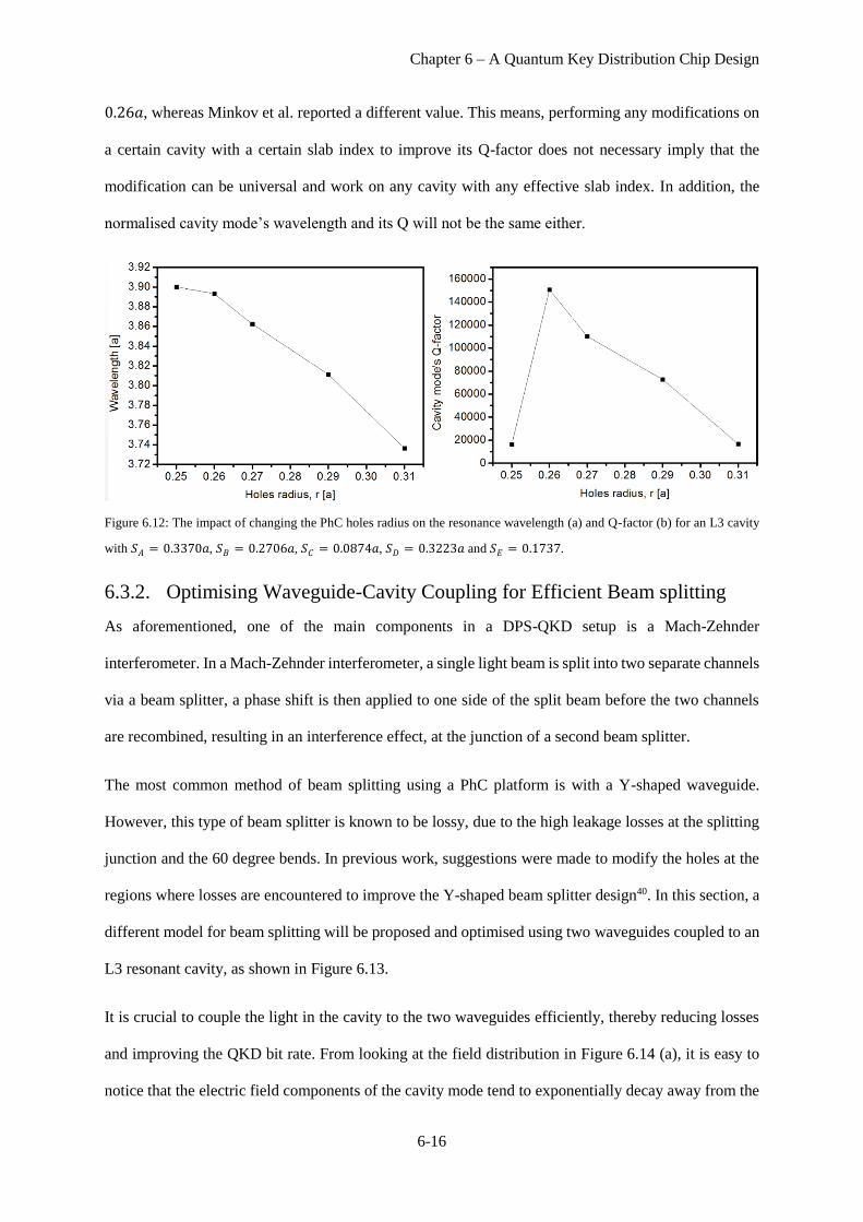
Chapter 6 – A Quantum Key Distribution Chip Design
6-16
0.26𝑎, whereas Minkov et al. reported a different value. This means, performing any modifications on
a certain cavity with a certain slab index to improve its Q-factor does not necessary imply that the
modification can be universal and work on any cavity with any effective slab index. In addition, the
normalised cavity mode’s wavelength and its Q will not be the same either.
Figure 6.12: The impact of changing the PhC holes radius on the resonance wavelength (a) and Q-factor (b) for an L3 cavity
with 𝑆𝐴 = 0.3370𝑎, 𝑆𝐵 = 0.2706𝑎, 𝑆𝐶 = 0.0874𝑎, 𝑆𝐷 = 0.3223𝑎 and 𝑆𝐸 = 0.1737.
6.3.2. Optimising Waveguide-Cavity Coupling for Efficient Beam splitting
As aforementioned, one of the main components in a DPS-QKD setup is a Mach-Zehnder
interferometer. In a Mach-Zehnder interferometer, a single light beam is split into two separate channels
via a beam splitter, a phase shift is then applied to one side of the split beam before the two channels
are recombined, resulting in an interference effect, at the junction of a second beam splitter.
The most common method of beam splitting using a PhC platform is with a Y-shaped waveguide.
However, this type of beam splitter is known to be lossy, due to the high leakage losses at the splitting
junction and the 60 degree bends. In previous work, suggestions were made to modify the holes at the
regions where losses are encountered to improve the Y-shaped beam splitter design40. In this section, a
different model for beam splitting will be proposed and optimised using two waveguides coupled to an
L3 resonant cavity, as shown in Figure 6.13.
It is crucial to couple the light in the cavity to the two waveguides efficiently, thereby reducing losses
and improving the QKD bit rate. From looking at the field distribution in Figure 6.14 (a), it is easy to
notice that the electric field components of the cavity mode tend to exponentially decay away from the

Chapter 6 – A Quantum Key Distribution Chip Design
6-17
cavity through the photonic structure at angles of 45, 135, 270 and 315 degrees, relative to the positive
x-axis of the slice. The radiative decay at these angles can be exploited to selectively position a
waveguide that the cavity can couple to efficiently. For this reason, a tilted cavity positioned next to
two L waveguides is suggested for optimised coupling efficiency. Figure 6.13 shows a rendered image
of the tilted cavity design modified according to cavity design 1, with two waveguides coupled to its
ends for efficient light beam splitting.
In previous work by Faron et al.40 where they demonstrated coupling tilted cavities to waveguides, the
Q-factor was shown to be directly dependent on the number of holes that separate the cavity and the
waveguide. Reducing the number of holes leads to higher leakage from the cavity to the waveguide,
thereby reducing the cavity’s Q-factor. In that work, the coupling was investigated by measuring the Q-
factor ratios between that of the cavity and the waveguide. A more rigorous method to estimate this
involves directly computing the power flux coupled to the waveguide in the two separate cases.
By coupling the horizontal cavity design 1 to two waveguides, where the index of the PhC’s dielectric
material matches that of GaAs at 915 nm, it was found that the Q-factor reduces to 3.4 × 10³. On the
other hand, the Q-factor achieved by coupling the optimised tilted design 1 to two waveguides is 3.6 ×
Figure 6.13: The proposed method of light beam splitting at the cavity as an alternative to Y shaped PhCs beam splitters.
Having the cavity oriented in this way allows the tails of the cavity mode to align with the waveguide.

Chapter 6 – A Quantum Key Distribution Chip Design
6-18
103. By recording the flux through either of the two waveguides that are coupled to the cavity, the ratio
between power fluxes transmitted from a tilted and a horizontal cavity is calculated, hence the
enhancement in coupling efficiency. It is important to mention that this method of measuring the
coupling efficiency enhancement can only be done when the simulation time steps for both cases is the
same and the difference in the cavity Q-factor is negligible. If this wasn’t the case, confinement
differences between the horizontal and the tilted cavity would lead to differences in light leakage
through the waveguide and hence the collected power flux.
Figure 6.14: The electric field distribution for the optimised horizontal (a) and tilted (b) cavity coupled waveguides. The figure
shows a clear increase in the field distribution along the waveguides that are coupled to a titled cavity due to an increased
coupling efficiency.
Figure 6.15: The power fluxes collected from the end of one of the two waveguides that are coupled to the cavity. The figure
shows clear enhancement in the collected power flux from a tilted cavity compared to a horizontal cavity, while maintaining
similar Q-factors between the two cases.

Chapter 6 – A Quantum Key Distribution Chip Design
6-19
Figure 6.15 shows that there is over 300% enhancement in the collected flux from the cavity; this is
larger than similar work done previously41. Interestingly, the coupling of higher order modes and/or
edge state modes to the waveguides diminish when a tilted cavity structure is used. This may mean that
these states might not exist within a tilted cavity, and if they do they will be in other wavelength ranges.
6.3.3. Y junction Photonic Crystal Beam splitters for Integrated QKD Systems
While two waveguides optimally coupled to a tilted cavity can serve as an effective beam splitter
scheme for QKD, an optimised Y shaped beam splitter based on PhCs is necessary to realise an efficient
Mach-Zehnder interferometer on Bob’s side. In this work, we will briefly discuss a method in which
light can be efficiently split into two arms with little reflection at the Y-junction; this method was
suggested initially in reference 42. In this section, the aim is to quantify the effect of modifying the Y-
junction by measuring the power flux collected at the end of the beam splitter’s arms using a flux region,
hence providing better estimate to the enhancement obtained by modifying the beam splitter. The
splitting efficiency of an unmodified beam spliter design similar to the one shown in Figure 6.16 (a) is
first measured. The beam splitter is then modified as shown in Figure 6.16 (b). The modification
involves adding an extra hole at the Y-junction with 𝑟 = 0.23𝑎 which is shifted by 𝑆 = 0.30𝑎. After
simulating the two different cases, the results were presented in Figure 6.17. From the Ey field
distribution, it is easy to see even splitting of the light in the two arms in the modified beam splitter.
Furthermore, the field in the two arms is much less intense when an unmodified beam splitter is used.
This becomes much more obvious when the flux spectrum is output Figure 6.17 (b). It is clear to see
that modifying the beam splitter has caused the power coupled to the arms to approximately double.
This means that over 50% of the power is lost at the Y-junction when an unmodified beam splitter is
used. In a QKD arrangement similar to the one shown in Figure 6.1, which typically uses 5 beam
splitters, losses like these due to poor beam splitter design can cause a large reduction in the achievable
bit rate.

Chapter 6 – A Quantum Key Distribution Chip Design
6-20
Figure 6.16: Schematics images of the unmodified (a) and the proposed modified (b) beam splitter. The modification is made
by adding a smaller hole, with 𝑟 = 0.23𝑎, shifted by 𝑆 = 0.30𝑎,
Figure 6.17: The field distribution inside a modified Y beam splitter structure (left) and the power flux spectrum (right)
obtained from modifying the beam splitter structure as per Figure 6.16.
6.3.4. Optimised Light Out-Coupling Efficiency from a Photonic Crystal
Waveguide
In this section, a study was carried out to investigate variations in the collected flux as the out-coupler
is displaced along the PhC waveguide. This was performed to find the out-coupler’s ideal position in
which the collection efficiency is optimised. To perform this study, a simulation was setup to measure
the flux spectra at the end of a PhC waveguide (before the out-coupler), and after the out-coupler, as
shown by the red rectangles in Figure 6.18. The Bragg out-coupler is designed to have alternating half
circular rings of width 𝜆 4𝑛⁄ where n is the refractive index of GaAs. These Bragg mirror based out-
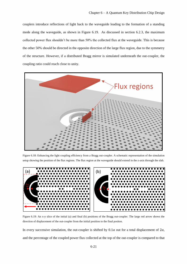
Chapter 6 – A Quantum Key Distribution Chip Design
6-21
couplers introduce reflections of light back to the waveguide leading to the formation of a standing
mode along the waveguide, as shown in Figure 6.19. As discussed in section 6.2.3, the maximum
collected power flux shouldn’t be more than 50% the collected flux at the waveguide. This is because
the other 50% should be directed in the opposite direction of the large flux region, due to the symmetry
of the structure. However, if a distributed Bragg mirror is simulated underneath the out-coupler, the
coupling ratio could reach close to unity.
Figure 6.18: Enhancing the light coupling efficiency from a Bragg out-coupler. A schematic representation of the simulation
setup showing the position of the flux regions. The flux region at the waveguide should extend in the z-axis through the slab.
Figure 6.19: An x-y slice of the initial (a) and final (b) positions of the Bragg out-coupler. The large red arrow shows the
direction of displacement of the out-coupler from the initial position to the final positon.
In every successive simulation, the out-coupler is shifted by 0.1𝑎 out for a total displacement of 2𝑎,
and the percentage of the coupled power flux collected at the top of the out-coupler is compared to that
𝝀𝒄𝒂𝒗
𝟒𝒏
𝝀𝒄𝒂𝒗
𝟒
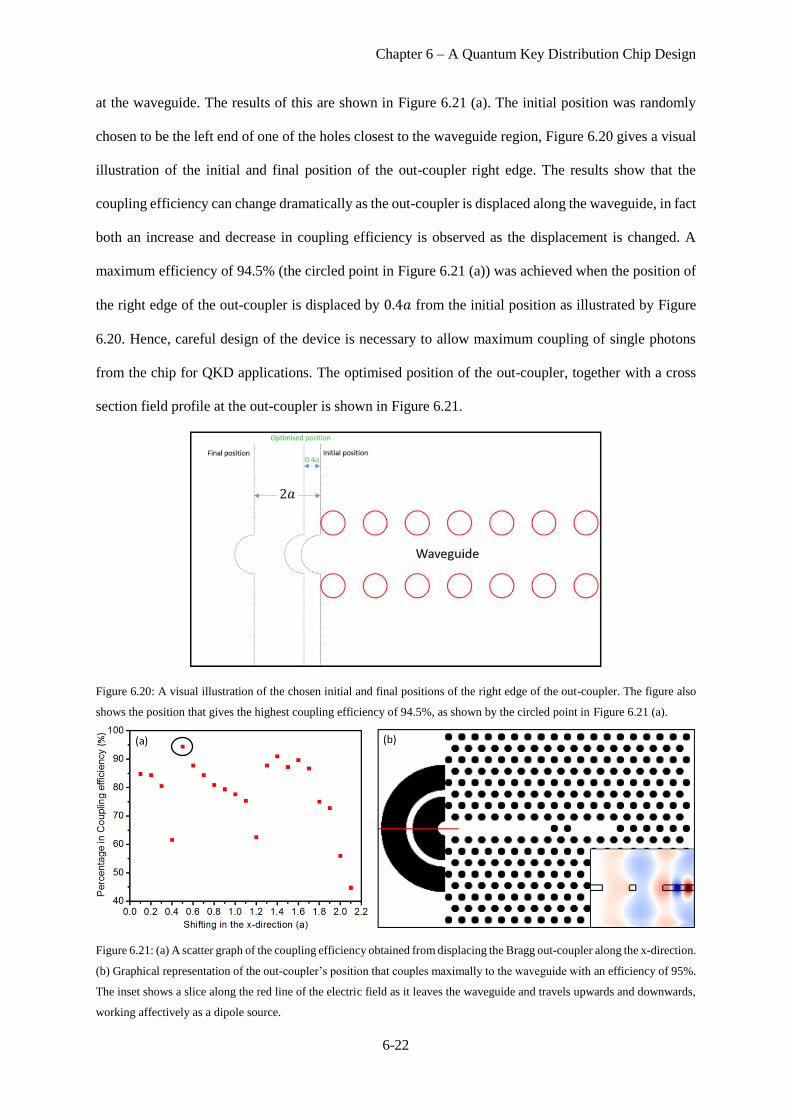
Chapter 6 – A Quantum Key Distribution Chip Design
6-22
at the waveguide. The results of this are shown in Figure 6.21 (a). The initial position was randomly
chosen to be the left end of one of the holes closest to the waveguide region, Figure 6.20 gives a visual
illustration of the initial and final position of the out-coupler right edge. The results show that the
coupling efficiency can change dramatically as the out-coupler is displaced along the waveguide, in fact
both an increase and decrease in coupling efficiency is observed as the displacement is changed. A
maximum efficiency of 94.5% (the circled point in Figure 6.21 (a)) was achieved when the position of
the right edge of the out-coupler is displaced by 0.4𝑎 from the initial position as illustrated by Figure
6.20. Hence, careful design of the device is necessary to allow maximum coupling of single photons
from the chip for QKD applications. The optimised position of the out-coupler, together with a cross
section field profile at the out-coupler is shown in Figure 6.21.
Figure 6.20: A visual illustration of the chosen initial and final positions of the right edge of the out-coupler. The figure also
shows the position that gives the highest coupling efficiency of 94.5%, as shown by the circled point in Figure 6.21 (a).
Figure 6.21: (a) A scatter graph of the coupling efficiency obtained from displacing the Bragg out-coupler along the x-direction.
(b) Graphical representation of the out-coupler’s position that couples maximally to the waveguide with an efficiency of 95%.
The inset shows a slice along the red line of the electric field as it leaves the waveguide and travels upwards and downwards,
working affectively as a dipole source.

Chapter 6 – A Quantum Key Distribution Chip Design
6-23
Assembling a Chip-Scale QKD System
After discussing and optimising cavities, waveguides, phase modulators and out-couplers for out-of-
chip coupling, the DPS-QKD chip can be discussed as a whole, as illustrated in Figure 6.22.
As shown previously in Figure 6.1, the DPS-QKD system starts with a single photon source. In this
work, this was proposed to be an InAs QD, coupled to either of the optimised cavity designs 1 or 2.
After the source, the photons are split into two arms. This was proposed to be accomplished by coupling
two waveguides to a tilted cavity. Using two waveguides directly coupled to the cavity helps to reduce
losses that can be encountered if a Y junction PhC beam splitter was used. The cavity is suggested to
be tilted to improve light coupling to the waveguides. Photons that travel through one arm should
encounter a phase modulation compared to the other. This is suggested through use of a PhC phase
modulator. The light is then coupled out of the chip through both arms using a Bragg mirror out-coupler.
The position of the out-coupler with respect to the PhC waveguide is necessarily tuned according to the
simulations performed in section 6.3.4 for optimum light out-coupling and reduced reflections at the
waveguide-out-coupler interface. Ideally, a distributed Bragg mirror tuned to the InAs QD wavelength
can be used underneath the out-coupler to reflect downward travelling photons to the collecting optics
above the chip. The photons from either arm are then collected and combined through a fibre beam
splitter before travelling to the receiver.
Preliminary Experimental Results for Photonic Crystals
Using GaSb QDs
GaSb QDs are type-two systems that have an extremely large hole confinement potential, resulting in
efficient operation at room temperature. Furthermore, by manipulating their growth, quantum rings can
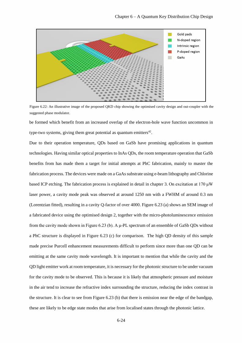
Chapter 6 – A Quantum Key Distribution Chip Design
6-24
be formed which benefit from an increased overlap of the electron-hole wave function uncommon in
type-two systems, giving them great potential as quantum emitters42.
Due to their operation temperature, QDs based on GaSb have promising applications in quantum
technologies. Having similar optical properties to InAs QDs, the room temperature operation that GaSb
benefits from has made them a target for initial attempts at PhC fabrication, mainly to master the
fabrication process. The devices were made on a GaAs substrate using e-beam lithography and Chlorine
based ICP etching. The fabrication process is explained in detail in chapter 3. On excitation at 170 μW
laser power, a cavity mode peak was observed at around 1250 nm with a FWHM of around 0.3 nm
(Lorentzian fitted), resulting in a cavity Q-factor of over 4000. Figure 6.23 (a) shows an SEM image of
a fabricated device using the optimised design 2, together with the micro-photoluminescence emission
from the cavity mode shown in Figure 6.23 (b). A μ-PL spectrum of an ensemble of GaSb QDs without
a PhC structure is displayed in Figure 6.23 (c) for comparison. The high QD density of this sample
made precise Purcell enhancement measurements difficult to perform since more than one QD can be
emitting at the same cavity mode wavelength. It is important to mention that while the cavity and the
QD light emitter work at room temperature, it is necessary for the photonic structure to be under vacuum
for the cavity mode to be observed. This is because it is likely that atmospheric pressure and moisture
in the air tend to increase the refractive index surrounding the structure, reducing the index contrast in
the structure. It is clear to see from Figure 6.23 (b) that there is emission near the edge of the bandgap,
these are likely to be edge state modes that arise from localised states through the photonic lattice.
Figure 6.22: An illustrative image of the proposed QKD chip showing the optimised cavity design and out-coupler with the
suggested phase modulator.
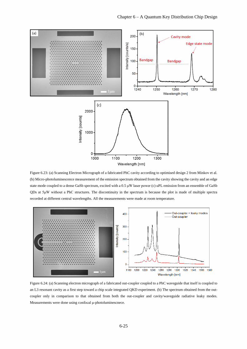
Chapter 6 – A Quantum Key Distribution Chip Design
6-25
Figure 6.23: (a) Scanning Electron Micrograph of a fabricated PhC cavity according to optimised design 2 from Minkov et al.
(b) Micro-photoluminescence measurement of the emission spectrum obtained from the cavity showing the cavity and an edge
state mode coupled to a dense GaSb spectrum, excited with a 0.5 μW laser power (c) uPL emission from an ensemble of GaSb
QDs at 5μW without a PhC structures. The discontinuity in the spectrum is because the plot is made of multiple spectra
recorded at different central wavelengths. All the measurements were made at room temperature.
Figure 6.24: (a) Scanning electron micrograph of a fabricated out-coupler coupled to a PhC waveguide that itself is coupled to
an L3 resonant cavity as a first step toward a chip scale integrated QKD experiment. (b) The spectrum obtained from the out-
coupler only in comparison to that obtained from both the out-coupler and cavity/waveguide radiative leaky modes.
Measurements were done using confocal μ-photoluminescnece.
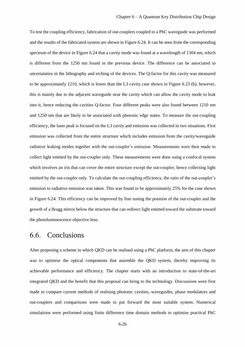
Chapter 6 – A Quantum Key Distribution Chip Design
6-26
To test the coupling efficiency, fabrication of out-couplers coupled to a PhC waveguide was performed
and the results of the fabricated system are shown in Figure 6.24. It can be seen from the corresponding
spectrum of the device in Figure 6.24 that a cavity mode was found at a wavelength of 1304 nm, which
is different from the 1250 nm found in the previous device. The difference can be associated to
uncertainties in the lithography and etching of the devices. The Q-factor for this cavity was measured
to be approximately 1210, which is lower than the L3 cavity case shown in Figure 6.23 (b), however,
this is mainly due to the adjacent waveguide near the cavity which can allow the cavity mode to leak
into it, hence reducing the cavities Q-factor. Four different peaks were also found between 1210 nm
and 1250 nm that are likely to be associated with photonic edge states. To measure the out-coupling
efficiency, the laser peak is focused on the L3 cavity and emission was collected in two situations. First
emission was collected from the entire structure which includes emission from the cavity/waveguide
radiative leaking modes together with the out-coupler’s emission. Measurements were then made to
collect light emitted by the out-coupler only. These measurements were done using a confocal system
which involves an iris that can cover the entire structure except the out-coupler, hence collecting light
emitted by the out-coupler only. To calculate the out-coupling efficiency, the ratio of the out-coupler’s
emission to radiative emission was taken. This was found to be approximately 25% for the case shown
in Figure 6.24. This efficiency can be improved by fine tuning the position of the out-coupler and the
growth of a Bragg mirror below the structure that can redirect light emitted toward the substrate toward
the photoluminescence objective lens.
Conclusions
After proposing a scheme in which QKD can be realised using a PhC platform, the aim of this chapter
was to optimise the optical components that assemble the QKD system, thereby improving its
achievable performance and efficiency. The chapter starts with an introduction to state-of-the-art
integrated QKD and the benefit that this proposal can bring to the technology. Discussions were first
made to compare current methods of realising photonic cavities, waveguides, phase modulators and
out-couplers and comparisons were made to put forward the most suitable system. Numerical
simulations were performed using finite difference time domain methods to optimise practical PhC

Chapter 6 – A Quantum Key Distribution Chip Design
6-27
cavities and efficiently couple them to PhC waveguides. To enhance out-of-chip coupling efficiency,
numerical simulations were also performed to optimise the out-coupling efficiency of light from the
chip using a Bragg mirror out-coupler. Enhancement in the coupling efficiency at Y-junction beam
splitters was also performed and coupling of over 90% was achieved. After proposing and optimising
all the necessary components to realise a DPS-QKD system, a potential design model for a typical
‘Alice’ chip was shown which involves the optimised tilted cavity coupled to the newly proposed beam
splitting scheme by coupling the cavity to two waveguides. Contacts for phase modulation were
fabricated around one arm of the waveguide, whilst doping the waveguide to create p-i-n regions
provided a reduction of the distance between the two electrodes, thereby creating a higher electric field
to minimise the waveguide’s length and the voltage needed for phase modulation.

Chapter 6 – A Quantum Key Distribution Chip Design
6-28
Bibliography
1 N. Gisin, G. Ribordy, W. Tittel, H. Zbinden. Quantum cryptography. Rev. Mod. Phys., 74, 145-195
(2002)
2 H. Lo, M. Curty, K. Tamaki. Secure quantum key distribution. Nature Photon., 8, 595-604 (2014)
3 V. Scarani, H. Bechmann-Pasquinucci, N. Cerf, M. Dusek, N. Lutkenhaus, M. Peev. The security of
practical quantum key distribution. Rev. Mod. Phys., 81, 1301-1350 (2009)
4 C. Bennett, G. Brassar. Quantum cryptography: public key distribution and coin tossing. In
Proceedings of IEEE International Conference on Computers, Systems and Signal Processing, 175, 8-
12 (1984)
5 K. Inoue, E. Waks, Y. Yamamoto. Differential Phase shift quantum key distribution. Phys. Rev. Lett.,
89, 037902 (2002)
6 J. Wang, A. Santamato, P. Jiang, D. Bonneau, E. Engin, J. W. Silverstone, M. Lermer, J. Beetz, M.
Kamp, S. Hofling, M. G. Tanner, C. M. Natarajan, R. H. Hadfield, S. N. Dorenbos, V. Zwiller, J. L.
O’Brien, M. G. Thompson. Gallium arsenide (GaAs) quantum photonic waveguide circuits. Optics
Communications, 327, 49-55 (2014)
7 H. C. Nguyen, S. Hashimoto, M. Shinkawa, T. Baba. Compact and fast photonic crystal silicon optical
modulators. Optics Express., 20, 22465-22474 (2012)
8 Q. Lu, W. Guo, D Byrene, J. F. Donegan. Design of low Vπ high-speed GaAs travelling-wave
electrooptic phase modulators using an n-i-p-n structure. IEEE Photonic Technology Letters, 20, 1805-
1807 (2008)
9 P. Sibson, C. Erven, M. Godfrey, S. Miki, T. Yamashita, M. Fujiwara, M. Sasaki, H. Terai, M. G.
Tanner, C. M. Natarajan, R. H. Hadfield, J. L. O’Brien, M. G. Thompson. Chip-based quantum key
distribution. Nature Commun., 13984 (2017)
10 G. Brassard, N. Lutkenhaus, T. Mor, B. C. Sanders. Limitations on practical quantum cryptography.
Phys. Rev. Lett, 85, 1330-1333 (2000)
11 M. D. Eisaman, J. Fan, A. Migdall, S. V. Polyakov. Invited review article: single-photon sources and
detectors. Rev. Sci. Instrum., 82, 071101 (2011)
12 L. Landin, M. S. Miller, M. E. Pistol, C. E. Pryor, L. Samuelson. Optical studies of individual InAs
quantum dots in GaAs: few-particle effects. Science, 280, 262-264 (1998)
13 X. Ding, Y. He, Z. C. Duan, N. Gregersen, M. C. Chen, S. Unsleber, S. Maier, C. Schneider, M.
kamp, S. Hofling, C. Lu, J. Pan. On-demand single photons with high extraction efficiency and near-
unity indistinguishability from a resonantly driven quantum dot in a micropillar. Phys. Rev. Lett., 116,
020401 (2016)
14 X. Ziang, L. Shifeng, Q. Laixiang, P. Shuping, W. Wei, Y. Yu, Y. Li, C. Zhijian, W. Shufeng, D.
Honglin, Y. Minghui, G. G. Qin. Refractive index and extinction coefficient of CH3NH3PbI3 studied by
spectroscopic ellipsometry. Optical Material Express, 5, 29-43 (2015)

Chapter 6 – A Quantum Key Distribution Chip Design
6-29
15 M. McClish, R. Farrell, K. Vanderpuye, K. S. Shah. A re-examination of silicon avalanche photodiode
gain and quantum efficiency. IEEE Nuclear Science Symposium Conference Record, DOI:
10.1109/NSSMIC.2005.1596952 (2005)
16 A. Schwagmann, S. Kalliakos, I. Farrer, J. P. Griffiths, G. A. C. Jones, D. A. Ritchie, A. J. Shields.
On-chip single photon emission from an integrated semiconductor quantum dot into a photonic crystal
waveguide. Appl. Phys. Lett., 99, 261108 (2011)
17 D. G. Gevaux, A. J. Bennett, R. M. Stevenson, A. J. Shields, P. Atkinson, J. Griffiths, D. Anderson,
G. A. C. Jones, D. A. Ritchie. Enhancement and suppression of spontaneous emission by temperature
tuning InAs quantum dots to photonic crystal cavities. Appl. Phys. Lett., 88, 131101 (2006)
18 A. Javadi, I. Sollner, M. Arcari, S. Lindskov Hansen, L. Midolo, S. Mahmoodian, G. Kirsanske, T.
Pregnolato, E. H. Lee, J. D. Song, S. Stobbe, P. Lodahl. Single-photon non-linear optics with a quantum
dot in a waveguide. Nature Commun., 6, 8655 (2015)
19 P. Lodahl, S. mahmoodian, S. Stobbe. Interfacing single photons and single quantum dots with
photonic nanostructures, Rev. Mod. Phys., 87, 347-400 (2015)
20 S. Tomic, J. Pal, M. Migilorato, R. J. Young, N. Vukmirovic. Visible spectrum quantum light sources
based on InxGa1-xN/GaB quantum dots. ACS Photonics, 2, 958-963 (2015)
21 C. Santori, M. Pelton, G. Solomon, Y. Dale, Y. Yamamoto. Triggered single photons for a quantum
dot. Phys. Rev. let., 86, 1502-1505 (2001)
22 M. Holmes, K. Choi, S. Kako, M. Arita, Y. Arakawa. Room temperature triggered single photon
emission from a III-Nitride site controlled nanowire quantum dot. Nano Lett., 14, 982-986 (2014).
23 H. J. Kimble, M. Dagenais, L. Mande, Photon antibunching in resonance fluorescence. Phys. Rev.
Lett., 39, 691-695 (1977)
24 F. Diedrich, H. Walther. Nonclassical radiation of a single stored ion. Phys. Rev. Lett., 58, 203-206
(1987)
25 C. Jurtsiefer, S. Mayer, P. Zarda, H. Weinfurter. Stable solid-state source of single photons. Phys.
Rev. Lett., 85, 290-293 (2000)
26 K. Srinivasan, O. Painter. Linear and nonlinear optical spectroscopy of a strongly coupled microdisk-
quantum dot system. Nature, 450, 862-865 (2007)
27 K. Hennessy, A. Badolato, M. Winger, D. Gerace, M. Atature, S. Gulde, S. Fält, E. L. Hu, A. Imam
Oğlu. Quantum nature of a strongly coupled single quantum dot-cavity system. Nature, 455, 896-899
(2007)
28 V. Loo, C. Arnold, O. Gazzano, A. Lemaitre, I. Sagnes, O. Krebs, P. Voisin, P. Senellart, L. Lanco.
Optical nonlinearity for few-photon pulses on a quantum dot-pillar cavity device. Phys. Rev. Lett., 109,
166806 (2012)
29 P. E. Barclay, K. Srinivasan, O. Painter, B. Lev, H. Mabuchi. Integration of fiber-coupled high-Q
SiNx microdisk with atom chips. Appl. Phys. Lett., 89, 131108 (2006)
30 U. K. Khankhoje, S-H. Kim, B. C. Richards, J. Hendrickson, J. Sweet, J. D. Olitzky, G. Khitrova, H.
M. Gibbs, A. Scherer. Modelling and fabrication of GaAs photonic-crystal cavities for cavity quantum
electrodynamics. Nanotechnology, 21, 065202 (2010)
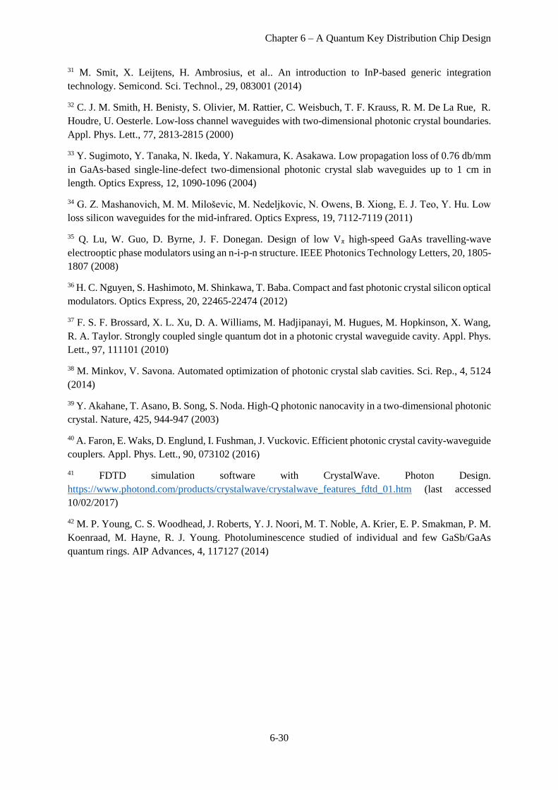
Chapter 6 – A Quantum Key Distribution Chip Design
6-30
31 M. Smit, X. Leijtens, H. Ambrosius, et al.. An introduction to InP-based generic integration
technology. Semicond. Sci. Technol., 29, 083001 (2014)
32 C. J. M. Smith, H. Benisty, S. Olivier, M. Rattier, C. Weisbuch, T. F. Krauss, R. M. De La Rue, R.
Houdre, U. Oesterle. Low-loss channel waveguides with two-dimensional photonic crystal boundaries.
Appl. Phys. Lett., 77, 2813-2815 (2000)
33 Y. Sugimoto, Y. Tanaka, N. Ikeda, Y. Nakamura, K. Asakawa. Low propagation loss of 0.76 db/mm
in GaAs-based single-line-defect two-dimensional photonic crystal slab waveguides up to 1 cm in
length. Optics Express, 12, 1090-1096 (2004)
34 G. Z. Mashanovich, M. M. Miloševic, M. Nedeljkovic, N. Owens, B. Xiong, E. J. Teo, Y. Hu. Low
loss silicon waveguides for the mid-infrared. Optics Express, 19, 7112-7119 (2011)
35 Q. Lu, W. Guo, D. Byrne, J. F. Donegan. Design of low Vπ high-speed GaAs travelling-wave
electrooptic phase modulators using an n-i-p-n structure. IEEE Photonics Technology Letters, 20, 1805-
1807 (2008)
36 H. C. Nguyen, S. Hashimoto, M. Shinkawa, T. Baba. Compact and fast photonic crystal silicon optical
modulators. Optics Express, 20, 22465-22474 (2012)
37 F. S. F. Brossard, X. L. Xu, D. A. Williams, M. Hadjipanayi, M. Hugues, M. Hopkinson, X. Wang,
R. A. Taylor. Strongly coupled single quantum dot in a photonic crystal waveguide cavity. Appl. Phys.
Lett., 97, 111101 (2010)
38 M. Minkov, V. Savona. Automated optimization of photonic crystal slab cavities. Sci. Rep., 4, 5124
(2014)
39 Y. Akahane, T. Asano, B. Song, S. Noda. High-Q photonic nanocavity in a two-dimensional photonic
crystal. Nature, 425, 944-947 (2003)
40 A. Faron, E. Waks, D. Englund, I. Fushman, J. Vuckovic. Efficient photonic crystal cavity-waveguide
couplers. Appl. Phys. Lett., 90, 073102 (2016)
41 FDTD simulation software with CrystalWave. Photon Design.
https://www.photond.com/products/crystalwave/crystalwave_features_fdtd_01.htm (last accessed
10/02/2017)
42 M. P. Young, C. S. Woodhead, J. Roberts, Y. J. Noori, M. T. Noble, A. Krier, E. P. Smakman, P. M.
Koenraad, M. Hayne, R. J. Young. Photoluminescence studied of individual and few GaSb/GaAs
quantum rings. AIP Advances, 4, 117127 (2014)

Chapter 7 – Conclusions and Future Work
7-1
Chapter 7
Conclusions and Future Work
Conclusions
In this thesis, potential approaches to realising optical components for integrated chip-scale quantum
key distribution (QKD) systems are numerically and experimentally studied. While the primary
application for carrying out research in this direction is QKD, these components can be utilised in many
other applications such as quantum computing, optical communication, metrology, sensing etc. Firstly,
numerical studies for coupling of transition metal dichalcogenides (TMDC) QDs with optical cavities
based on rod-type photonic crystals (PhC) were done for the first time to improve light-matter
interaction and provide enhancement in the light collection efficiency. Secondly, deterministic spatial
growth of III-V nanowires on silicon was achieved for single photon detection applications. Thirdly, a
proposal for integrating a QKD system using PhCs was presented for the first time. Numerical
optimisation of the individual components needed for QKD was achieved and initial fabrication results
were presented.
The single photon source is one of the most important components found in a typical QKD system. It
directly contributes to the bit rate and security of the distributed key in QKD. Chapter 4 of this thesis
aims at utilising the unique optical properties of TMDCs for realising integrable single photon sources.
A rod-type PhC cavity design was proposed to efficiently couple to TMDC monolayers. Compared to
using air-bridge hole-type PhC cavities, this technique, in principle provides optimised coupling

Chapter 7 – Conclusions and Future Work
7-2
between the cavity mode’s maximum and the light emitter. In addition, the reduced dielectric-to-air
volume ratio of rod-type PhCs minimises light absorption by the dielectric material. Finite difference
time-domain (FDTD) method was used to simulate the optical properties of the PhC cavity, output its
Q-factor and measure the enhancement in the collected flux emitted by a TMDC light source coupled
to the cavity. Simulations of a hexagonal lattice PhC show a bandgap forming for TE-like modes
between 1.05𝑎 < 𝜆 < 1.17𝑎. By observing the field profile for Ex and Ey, a cavity confinement mode
was found at λ = 1.12𝑎 with a Q-factor simulated to be more than 300 for 𝑟 = 0.165𝑎 and rods height
ℎ = 2.3𝑎. Next a flux region was setup above the cavity to mimic a photoluminescence objective with
numerical aperture of 0.65. A pulse source inside the cavity is initiated and the power flux transmitted
through a flux region is accumulated as the field decays from the cavity with time. The power flux is
compared to the case where the source is placed directly on the substrate without the presence of a rod-
type PhC structure. After comparing the power fluxes, it was found that the photonic cavity can provide
about 400 % enhancement in the light collection efficiency. To study the effect of variations in the rods’
radius on the extraction efficiency due to fabrication fluctuations, simulations were carried out for 𝑟
ranging from 0.155𝑎 to 0.170𝑎. Results have shown that maximum enhancement takes place when the
rods’ radius is 𝑟 = 0.161𝑎. The collected power flux starts to reduces, hence reducing the collection
enhancement to lower percentages as the radius deviates away from 𝑟 = 0.161𝑎. The comparison
between the different flux spectra as 𝑟 is varied has shown that reducing the radius of the rods causes a
blue-shift in the cavity mode’s energy, while increasing 𝑟 causes a red-shift in the cavity mode’s energy.
Numerical modelling was also carried out to investigate the effect of dipping the monolayer to different
heights within the cavity on the achieved enhancement in the collected light. Simulations were done
while the source position is moved from vertically from the bottom of the cavity to the top in steps. The
comparison between the different power flux spectra collected from every step showed maximum
enhancement when the source vertical height is near the central height of the rods where the cavity
mode’s maximum exists. The enhancement reduces as the source is moved toward the top of the rods
due to reduced spatial coupling between the emitter and the cavity mode. In addition coupling to
radiative modes to air causes further reduction in the enhancement ratio. The enhancement reduces as

Chapter 7 – Conclusions and Future Work
7-3
the source is moved downward, away from the central height of the rods. This is minimised at the
bottom of the cavity where coupling to substrate-mediated leaky modes becomes more dominant.
Experimental fabrication of rod-type PhCs using CSAR62 as a positive e-beam resist has been shown.
Cr was transferred to the substrate as a hard mask to provide high selectivity in the dry etch of Silicon.
Reactive ion etching technique was utilised to form the rods by etching silicon using SF6 and O2 gasses
at 130W RF power, achieving an etch rate of approximately 90nm per minute. The transfer of a
monolayer on the PhC was followed using the wet transfer method. Finally, results from successful PhC
fabrication and monolayer transfer were presented.
In a QKD system, single photon detectors are essential components that directly influence the achieved
key bit rate. Chapter 5 aims at advancing the recently emerged application of nanowire based
photodetectors to grow III-V nanowires on Si material in a spatially deterministic way. The unique
geometrical, electrical and optical properties of nanowires that make them superior over conventional
methods of realising photodetectors were discussed together with the current state research in the field.
Different methods of biasing free standing and drop-casted nanowires were introduced. Next, a proposal
was shown for optically coupling epitaxially grown free standing nanowires photodetector to a photonic
chip. For spatially selectively growing these nanowires, results from the fabrication of nanowire sites
using e-beam lithography were given. The e-beam CAD pattern is firstly corrected for proximity effects
using Beamer. The pattern is written by exposing a CSAR resist which was previously spin coated on
a Si/SiO2 substrate. The exposed regions are then developed in o-Xylene solution. The pattern is then
transferred to the oxide layer by wet etching with buffered oxide HF etcher. The resist is then stripped
from the substrate using acetone. Electron micrographs of the fabricated nanowire sites were shown for
the post-developing and post-etching stages. Enlargement in the transferred nanowire sites was
observed due to isotropic chemical etching of the oxide layer. Following the etching immediately,
epitaxial growth of InAs and GaAs nanowires was achieved using molecular beam epitaxy. Electron
micrographs show that the nanowire successfully seed on the etched nanowire sites where the silicon is
exposed, while almost no growth was observed above the oxide covered regions. However, this varies
dramatically with temperature as the longest achieved nanowires growth was found to take place within

Chapter 7 – Conclusions and Future Work
7-4
a small growth temperature window around 570 ºC. Growing at low wafer temperatures was found to
lead to the growth of short nanowires, this is likely to be attributed to reduced migration distance of the
nanowire’s composition material above the substrate. Operating at a higher substrate’s growth
temperatures provided enough migration of the composite material which caused growth within the
nanowires sites only, while left oxide regions clean. However, this was expected to have led to reducing
the amount of group V material available for the growth of nanowires due to their low evaporation
temperature. The growth ratio of nanowires per the number of available sites have been measured to be
over 70%. The micrographs have shown that all the nanowires exhibited hexagonal structures with
different symmetries. The variation of the symmetry could have been due to nanowires seeding on the
particle remains of SiO2 that were found to appear after wet etching the oxide layer. Results from
growing GaAs nanowires on nanowire sites fabricated in a similar way are shown. It was observed that
a large proportion of GaAs nanowires grew following the 111 facet. Optimising this could be done by
fine tuning the growth temperature and the material flow rate.
Prior to experimentally fabricating a photonic circuit for QKD, spending a large amount of effort for
modelling the components is essential for designing an optimised system with optimum efficiency.
Chapter 6 proposed a model to miniaturise conventional differential phase shift (DPS) QKD to a chip
level using PhCs as a platform for integrated photonic circuitry on GaAs. Single photon sources based
on InAs quantum dots (QDs) embedded in the bridge structure of a typical hole-type PhC cavity are
suggested. An L3 cavity design is proposed for Purcell enhancing light emission from InAs QDs by
increasing the field intensity within the vicinity of the emitter due to the cavity mode. Different
variations to the standard L3 cavity design were proposed and simulated using FDTD. The design was
optimised by investigating the effect of changing the holes’ radius on the standard cavity. As the radius
of the holes is increased, the cavity mode’s wavelength was found to reduce. Maximum Q factor for the
cavity was found with a radius 𝑟 = 0.3𝑎. Optimising the cavity’s design was carried out by shifting the
holes adjacent to the cavity, while measuring its achieved Q-factor. The first optimised design was
found by setting 𝑟𝐴 = 0.2𝑎, which formed a cavity with 𝑄 = 1.3 × 10⁵. Simulations have also shown
that the cavity mode’s volume blueshifts as 𝑟𝐴 is increased. The same relation was observed for H1

Chapter 7 – Conclusions and Future Work
7-5
cavities, the optimised Q-factor for H1 cavities was found for 𝑟𝐴 = 0.15𝑎 though. The second optimised
design was taken from literature, however, the work done in this chapter aimed at investigating the
optimised design with GaAs for wavelengths emitted by InAs QDs, in contrast to using Si material for
a cavity mode wavelength in the mid infrared spectrum as was presented in the original work.
Simulation results have shown that Q-factors over 1.5 × 10⁵ were achievable.
To extract single photons out from the cavity in a QKD chip, a PhC waveguide is spatially coupled to
the cavity to allow the confinement mode to leak into the waveguide mode. A study was carried out to
compare the enhancement in the power flux collected through a PhC waveguide when it is coupled to
a tilted and horizontal cavity. FDTD have shown over three times enhancement in the flux collected
from a waveguide with a tilted cavity compared to a horizontal cavity. This optimisation in principle
can lead to higher bitrate when utilised in a QKD chip.
A Mach-Zehnder is an important component in DPS-QKD systems. To reduce losses in a Mach-
Zehnder, optimised Y-junction beam splitters that have minimum losses is essential and was one of the
main motivations for carrying out this work. The simulation was performed by recording the flux as it
travels toward the Y-junction and at the arms of the beam splitter. A conventional Y-beam splitter was
optimised by adding a PhC hole at the beam splitter’s junction, where the holes have a smaller radius
compared to others in the crystal. This modification was found to greatly reduce scattered light at the
junction. This improved the light splitting and coupling to the two waveguides. Further optimisation of
the beam splitter could be done by modifying the PhC near the 60º bends to reduce scattering losses. It
is anticipated that increasing the diameters of the holes surrounding the bend can improve light bending
and dramatically reduces losses.
To couple the light efficiently from the photonic chip, a Bragg mirror out-coupler was investigated. The
effect of varying the position of a two layer Bragg out-coupler along the PhC waveguide was found to
effect the percentage of light emitted out by the out-coupler. Careful positioning of the out-coupler with
respect to the PhC holes that the crystal is composed of can lead to coupling efficiencies of as high as
95%. The optimised components are then collected together to make the final proposal of the chip-scale
QKD system. The system is composed of the optimised tilted cavity which is coupled to two waveguides

Chapter 7 – Conclusions and Future Work
7-6
one of which includes a PhC phase modulator. The waveguides are each coupled to the optimised out-
couplers.
Finally, preliminary results from testing the optimised PhC L3 fabricated on GaAs using GaSb as light
emitters were presented as a first step towards realising chip-scale QKD using PhCs.
Future Work
One of the main advantages of rod-type PhC cavity is allowing optimised coupling between the cavity
mode and a 2D emitter which increases light-matter interaction and provides enhancement in the light
extraction from these emitters. Performing computer simulations that can best predict experimental
results can only be done by including silicon’s absorption in the simulations. This could be done by
assigning complex refractive indices to the high dielectric material that resemble silicon. Absorption by
the dielectric rods and the substrate can lead to reduced cavity Q-factor and affect the extraction
efficiency ratio. In addition, placing a 2D monolayer above the cavity can cause perturbation to the
dielectric symmetry of the cavity structure, taking this into account may lead to reduction in the
achieved Q-factor, despite the fact that the perturbation might be very small.
In chapter 4, simulations were carried out to investigation the effect of varying the emitter’s height in
the cavity on the achieved enhancement. While emission from artificially created defects is promoted
when the monolayer is maximally strained, simulating changes in the extraction efficiency as the
emitter’s position is varied in the x-y plane is useful for a comprehensive study of the cavity. Finite
element methods of the dipping of the emitter can be utilised to help predicting the dipping of a
monolayer in the cavity.
Vertical light confinement is necessary to allow light guiding on-chip with minimum losses. One
method of achieving vertical confinement with rod-type PhCs can be accomplished by surrounding the
rods with an optically transparent material which could be realised by spin coating the chip or bottom
up growth of the material using chemical vapour deposition. The refractive index contrast between the
transparent material with air on top and the dielectric substrate at the bottom causes total internal
reflection. This technique has never been used with rod-type PhC structures but is expected to increase
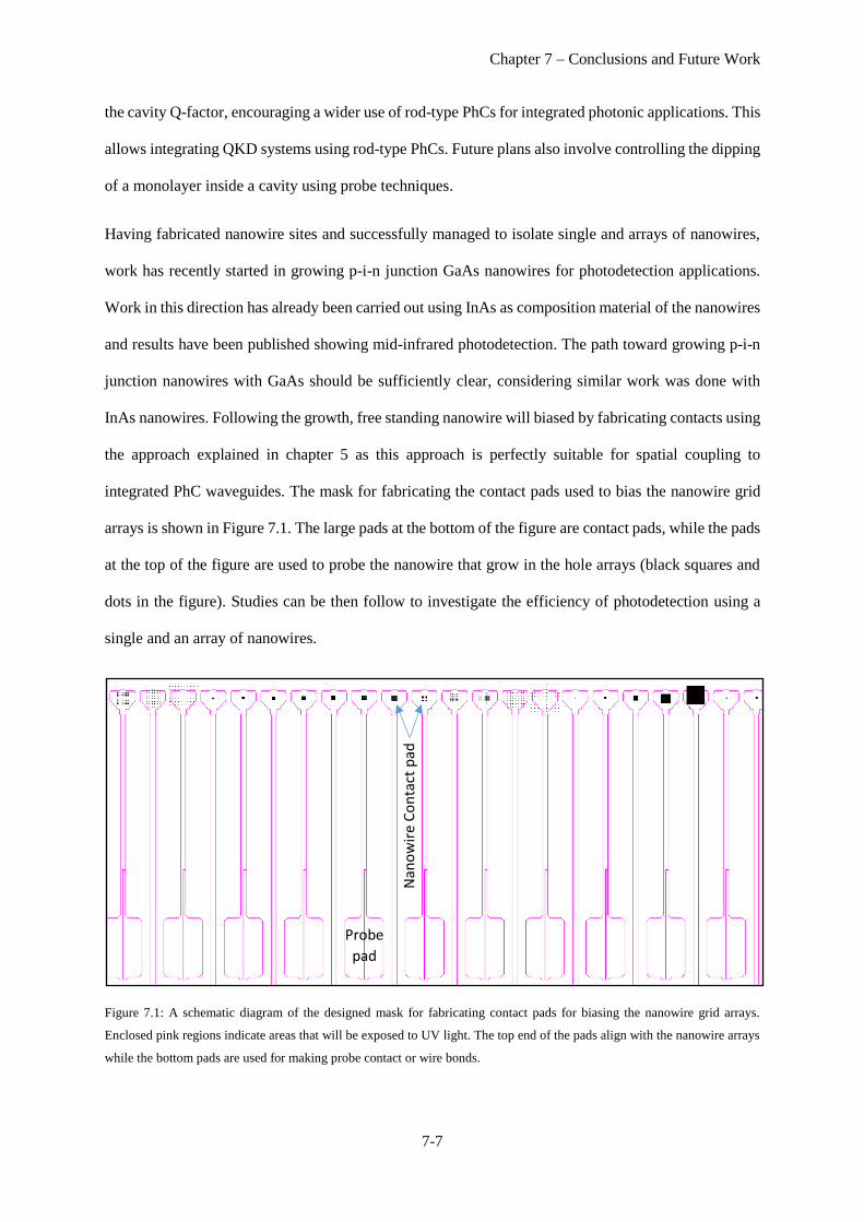
Chapter 7 – Conclusions and Future Work
7-7
the cavity Q-factor, encouraging a wider use of rod-type PhCs for integrated photonic applications. This
allows integrating QKD systems using rod-type PhCs. Future plans also involve controlling the dipping
of a monolayer inside a cavity using probe techniques.
Having fabricated nanowire sites and successfully managed to isolate single and arrays of nanowires,
work has recently started in growing p-i-n junction GaAs nanowires for photodetection applications.
Work in this direction has already been carried out using InAs as composition material of the nanowires
and results have been published showing mid-infrared photodetection. The path toward growing p-i-n
junction nanowires with GaAs should be sufficiently clear, considering similar work was done with
InAs nanowires. Following the growth, free standing nanowire will biased by fabricating contacts using
the approach explained in chapter 5 as this approach is perfectly suitable for spatial coupling to
integrated PhC waveguides. The mask for fabricating the contact pads used to bias the nanowire grid
arrays is shown in Figure 7.1. The large pads at the bottom of the figure are contact pads, while the pads
at the top of the figure are used to probe the nanowire that grow in the hole arrays (black squares and
dots in the figure). Studies can be then follow to investigate the efficiency of photodetection using a
single and an array of nanowires.
Figure 7.1: A schematic diagram of the designed mask for fabricating contact pads for biasing the nanowire grid arrays.
Enclosed pink regions indicate areas that will be exposed to UV light. The top end of the pads align with the nanowire arrays
while the bottom pads are used for making probe contact or wire bonds.
Probe
pad
Nan
ow
ire
Co
nta
ct p
ad
Chapter 7 – Conclusions and Future Work
7-8
Integrating a QKD system in hand held devices could only be achieved by miniaturizing single photon
detectors to the chip-level. For example light from Bob’s photonic circuit can be coupled to an external
off-the-shelf Si APD using beam out-couplers. The out-coupler directs the light from the waveguide
toward the detector chip which is typically situated adjacent to the measurement chip. The layer
structure of a QKD chip can also be grown so that both the Si APD detector layers and those required
for fabricating photonic crystals are done by molecular beam epitaxy or chemical vapour deposition.
Fabricating the detector’s contacts and the PhC can then follow using conventional lithography
techniques. Another approach to integrating the detectors used in QKD could emerge from successfully
realising nanowire based photodetectors. To achieve this, research is needed to be carried out to tune
the operation wavelength to match that of InAs QD’s emission.
Further work can be carried out to optimise light guiding in hole-type PhC waveguides by making
modification to its design. Increasing the confinements of these waveguides and reducing their losses
is essential for many applications other than QKD. Waveguides with lower losses can increase the QKD
bit rate in QKD and allows fabricating long phase modulators, reducing the voltage required to establish
high electric fields for short waveguides. This reduces heat resultant from operating at high switching
frequencies.
Successful growth and fabrication of the full QKD system will be followed by many measurements
such as photoluminescence, coupling efficiencies between the different optical components, losses by
the different components and key generation.
The QKD system discussed in this thesis uses the differential phase shift keying, however, polarisation
encoding QKD can also have strong integration potential on a chip scale. Each of these schemes have
advantages and disadvantages in their fabrication complexity, bit rate, achieved distance, etc, and the
best scheme should be chosen based on the QKD application the system is designed for.

Appendix A
A1
Appendix A
This Appendix contains an example of a MEEP code used to simulate an L3 hole-type photonic crystal
cavity embedded in GaAs bridge.
; resetting the software to
(reset-meep) ; clearing memory from MEEP
(define-param res 20) ; defines the pixel size of the simulation cell
(define-param edge-shift 0.15) ; shift of holes near the cavity
(define-param tdecay 500) ; define number of time step to run simulation
(define-param pad-holes 8) ; number of holes at each side
(define-param pad-air 1.5) ; thickness of air region above cavity
(define-param eps-gaas 12.827859) ; dielectric constant of GaAs
(define-param hole-radius 0.29) ; radius of holes
(define-param hole-radius2 0.20) ; radius of small holes near cavity
(define-param slab-thickness 0.5) ; bridge/slab thickness
(define-param dpml 1) ; width of pml layer
(define-param fcen 0.273712876505613) ; central frequency of source
(define-param df 0.1) ; spectral width of source
(define-param nfreq 10000) ; number of sampled frequencies
; switching off averaging dielectric values which is a feature in meep
(set! eps-averaging? false)
; defining the dimensions of simulation cell
(define sx (+ 2 (* 2 pad-holes) (* 2 dpml)))
(define sy (+ (* (sin (/ pi 3)) 2 pad-holes) (* 2 dpml)))
(define sz (+ slab-thickness (* 2 pad-air) (* 2 dpml)))
; setting dimension of simulation cell
(set! geometry-lattice (make lattice (size sx sy sz)))
; defining default material to be air
(set! default-material (make dielectric (material air)))
(set! pml-layers (list (make pml (thickness dpml)))) ; defining pml layer and dimensions
; setting up geometry of the bridge

Appendix A
A2
(set! geometry
(list
(make block
(center 0 0 0)
(size infinity infinity slab-thickness)
(material (make dielectric (epsilon eps-gaas))))))
; defining the array of PhC lattice
(set! geometry
(append geometry
; even rows above
(geometric-objects-duplicates
(vector3 0 (* 2 (sin (/ pi 3))) 0) 1 (/ pad-holes 2)
(geometric-object-duplicates
(vector3 -1 0 0) 0
(+ 2 (* 2 pad-holes))
(make cylinder
(center (+ 1 pad-holes) 0)
(radius hole-radius)
(height infinity)
(material air))))
; even rows below
(geometric-objects-duplicates
(vector3 0 (* 2 (sin (/ pi 3))) 0) (/ pad-holes -2) -1
(geometric-object-duplicates
(vector3 -1 0 0) 0
(+ 2 (* 2 pad-holes))
(make cylinder
(center (+ 1 pad-holes) 0)
(radius hole-radius)
(height infinity)
(material air))))
; odd rows
(geometric-objects-duplicates
(vector3 0 (* 2 (sin (/ pi 3))) 0)

Appendix A
A3
(/ pad-holes -2) (- (/ pad-holes 2) 1)
(geometric-object-duplicates
(vector3 -1 0 0) 0
(+ 1 (* 2 pad-holes))
(make cylinder
(center (+ pad-holes 0.5) (sin (/ pi 3)))
(radius hole-radius)
(height infinity)
(material air))))
; middle row
(geometric-object-duplicates
(vector3 -1 0 0) 0 (- pad-holes 2)
(make cylinder
(center -3 0 0)
(radius hole-radius)
(height infinity)
(material air)))
(geometric-object-duplicates
(vector3 1 0 0) 0 (- pad-holes 2)
(make cylinder
(center 3 0 0)
(radius hole-radius)
(height infinity)
(material air)))
; the offset cells
(list
(make cylinder
(center (+ 2 edge-shift) 0 0)
(radius hole-radius2)
(height infinity)
(material air))
(make cylinder
(center (- -2 edge-shift) 0 0)
(radius hole-radius2)

Appendix A
A4
(height infinity)
(material air)))))
; switching on mirror symmetry for quicker simulations
(set! symmetries (list (make mirror-sym (direction X) (phase 1))
(make mirror-sym (direction Z) (phase 1))
(make mirror-sym (direction Y) (phase -1))))
; setting up pixel size (resolution) of simulation cell
(set-param! resolution res)
; setting up source
(set! sources (list
(make source
(src (make gaussian-src (frequency fcen) (fwidth df)))
(component Ey)
(center 0 0 0))))
(define (print-mode-volume) (print ; measuring mode volume
"mode_volume: " (meep-time)
", " (electric-energy-in-box (meep-fields-total-volume fields))
", " (meep-fields-electric-energy-max-in-box fields (meep-fields-total-
volume fields))
", " (meep-fields-modal-volume-in-box fields (meep-fields-total-volume
fields))
"\n"))
; defining flux transmission region
(define trans
(add-flux fcen df nfreq
(make flux-region
(center 1 0 0) (size 0 1.5 1.5) (direction X))))
; setting up simulation parameters, such as time steps of simulation, outputting epsilon function, using
harminv to find modes and calculating their Q-factors, outputting mode volume and e-field profile.
(run-sources+ tdecay
(at-beginning output-epsilon)
(after-sources (harminv Ey (vector3 0 0 0) fcen df))
(after-sources+ (- tdecay (/ .25 fcen)) print-mode-volume)
(at-end output-efield-y))
(display-fluxes trans)