Embed Size (px)
Citation preview
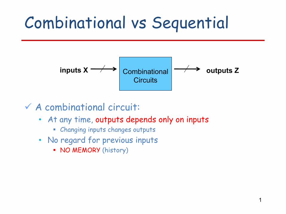
Combinational vs Sequential
A combinational circuit:• At any time, outputs depends only on inputs
Changing inputs changes outputs
• No regard for previous inputs NO MEMORY (history)
1
Combinational
Circuits
inputs X outputs Z
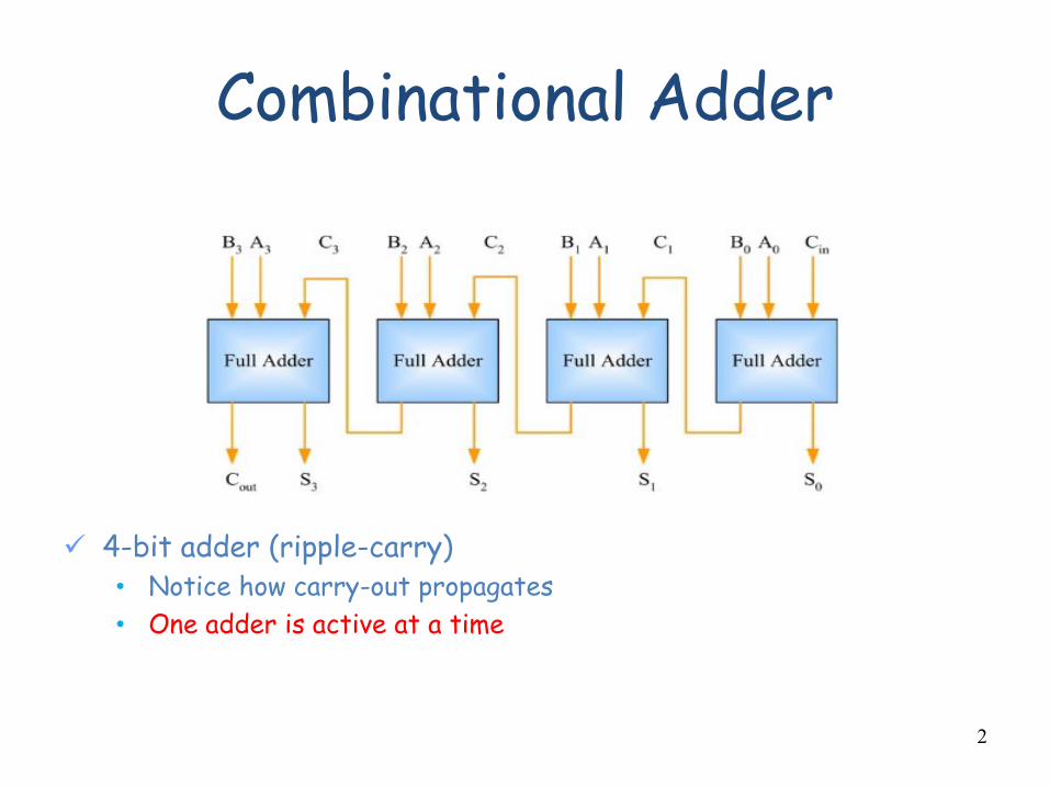
Combinational Adder
4-bit adder (ripple-carry)• Notice how carry-out propagates
• One adder is active at a time
2
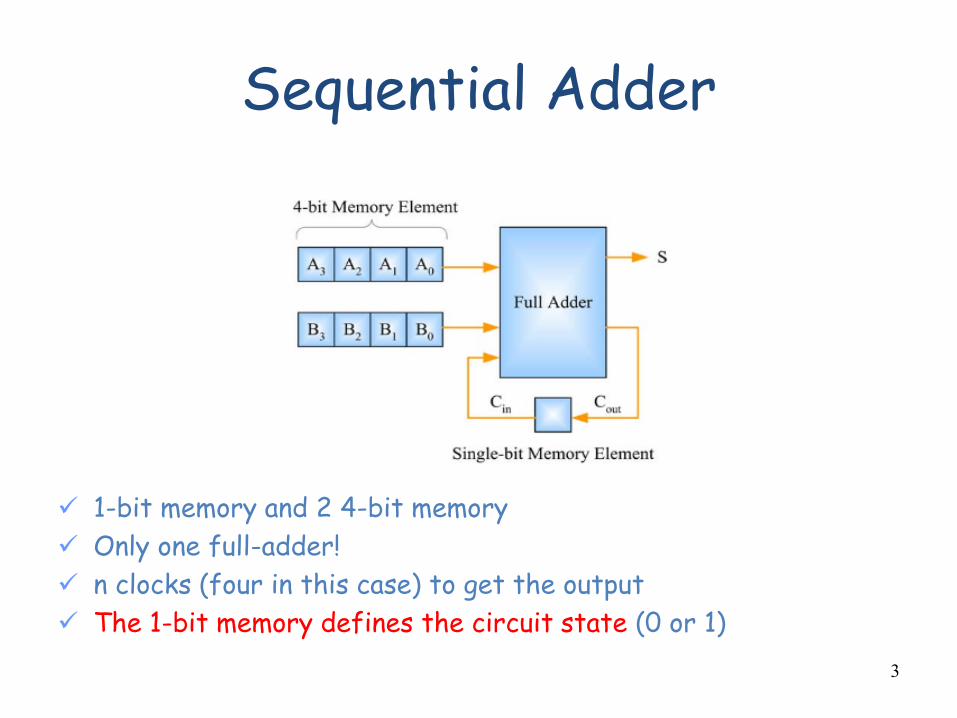
Sequential Adder
1-bit memory and 2 4-bit memory
Only one full-adder!
n clocks (four in this case) to get the output
The 1-bit memory defines the circuit state (0 or 1)
3
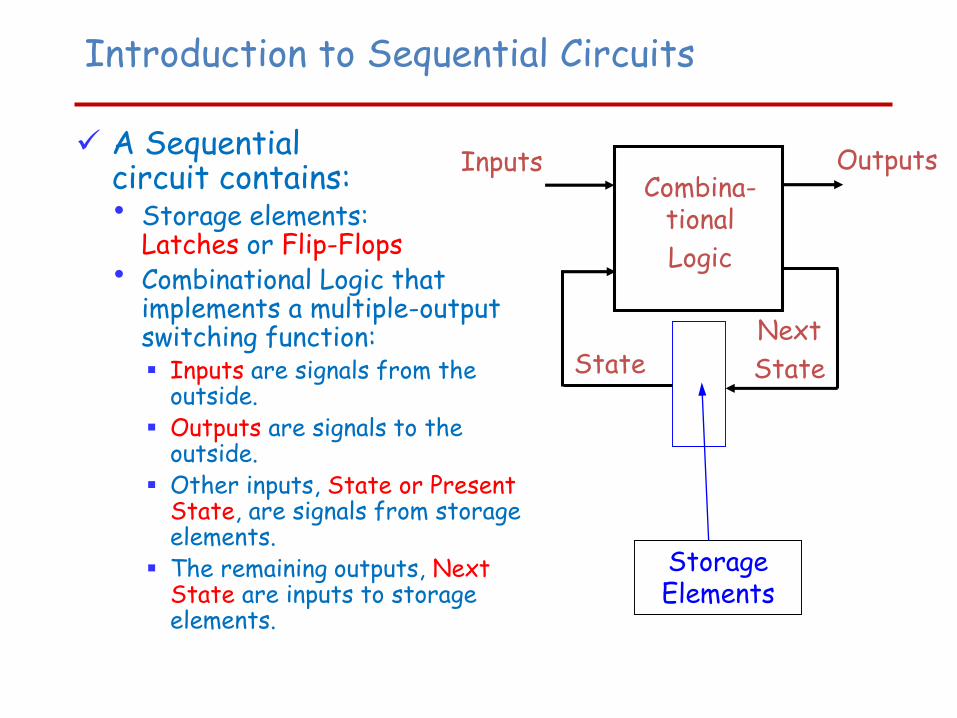
Introduction to Sequential Circuits
A Sequential circuit contains:• Storage elements:
Latches or Flip-Flops• Combinational Logic that
implements a multiple-output switching function: Inputs are signals from the
outside. Outputs are signals to the
outside. Other inputs, State or Present
State, are signals from storage elements.
The remaining outputs, Next State are inputs to storage elements.
Combina-tional
Logic
Storage Elements
Inputs Outputs
StateNext
State
Introduction to Sequential Circuits
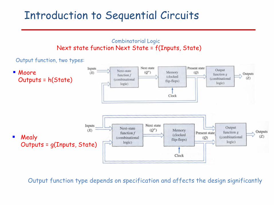
Output function type depends on specification and affects the design significantly
Combinatorial LogicNext state function Next State = f(Inputs, State)
Output function, two types:
MooreOutputs = h(State)
MealyOutputs = g(Inputs, State)
Types of Sequential Circuits
Depends on the times at which:• storage elements observe their inputs and change their state
Synchronous• Behavior is defined from knowledge of signals at discrete instances of
time• Storage elements observe inputs and can change state only in relation
to a timing signal (clock pulses from a clock)
Asynchronous• Behavior is defined from knowledge of inputs an any instant of time and
the order in continuous time in which inputs change• If clock just regarded as another input, all circuits are asynchronous!
Nevertheless, the synchronous abstraction makes complex designs tractable!
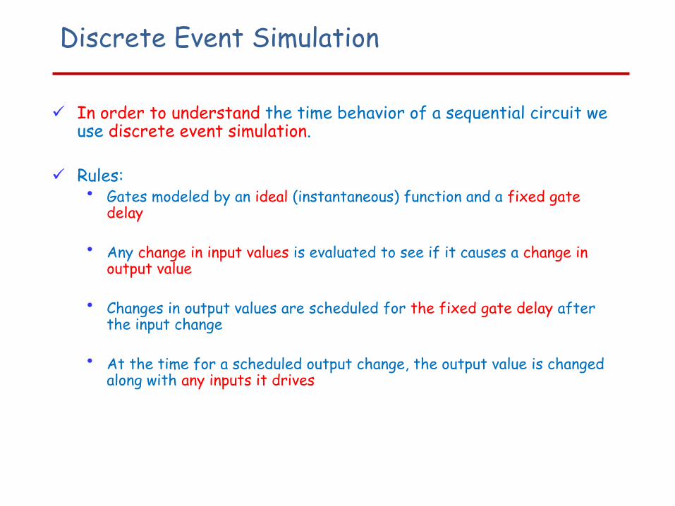
Discrete Event Simulation
In order to understand the time behavior of a sequential circuit we use discrete event simulation.
Rules:• Gates modeled by an ideal (instantaneous) function and a fixed gate
delay
• Any change in input values is evaluated to see if it causes a change in output value
• Changes in output values are scheduled for the fixed gate delay after the input change
• At the time for a scheduled output change, the output value is changed along with any inputs it drives
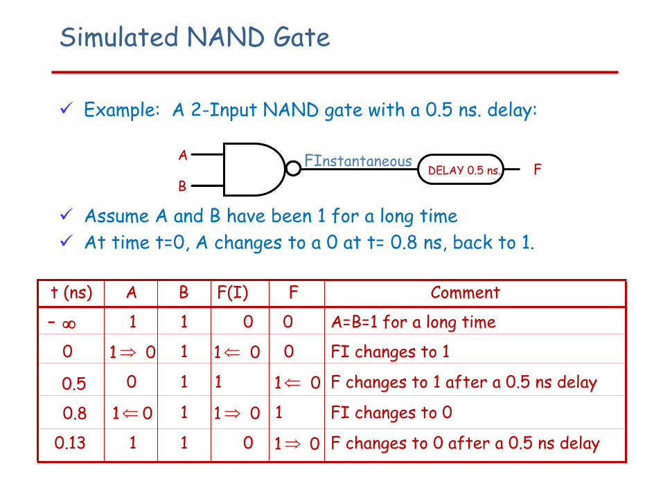
Simulated NAND Gate
Example: A 2-Input NAND gate with a 0.5 ns. delay:
Assume A and B have been 1 for a long time
At time t=0, A changes to a 0 at t= 0.8 ns, back to 1.
FA
B
FInstantaneous
t (ns) A B F(I) F Comment
– 1 1 0 0 A=B=1 for a long time
0 1 0 1 1 0 0 FI changes to 1
0.5 0 1 1 1 0 F changes to 1 after a 0.5 ns delay
0.8 1 0 1 1 0 1 FI changes to 0
0.13 1 1 0 1 0 F changes to 0 after a 0.5 ns delay
DELAY 0.5 ns.
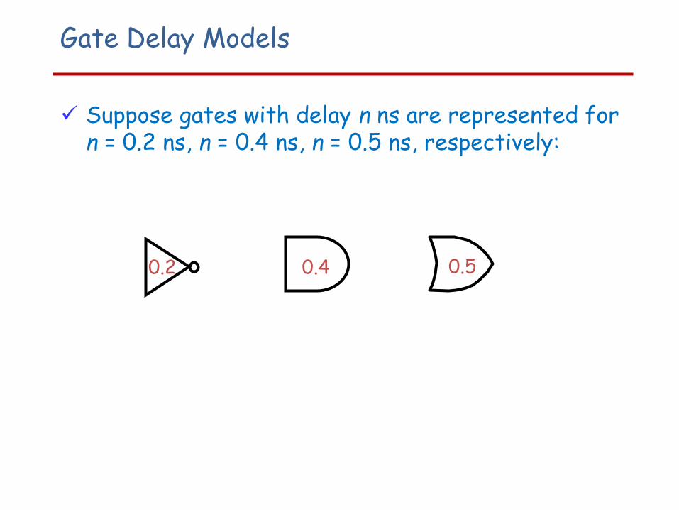
Gate Delay Models
Suppose gates with delay n ns are represented for n = 0.2 ns, n = 0.4 ns, n = 0.5 ns, respectively:
0.2 0.50.4
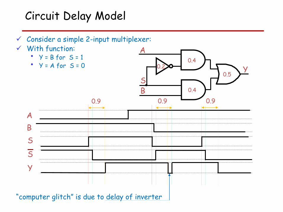
Consider a simple 2-input multiplexer: With function:
• Y = B for S = 1• Y = A for S = 0
“computer glitch” is due to delay of inverter
A
0.4
0.5
0.4
SB
Y0.2
Circuit Delay Model
A
S
B
Y
S
0.9 0.9 0.9
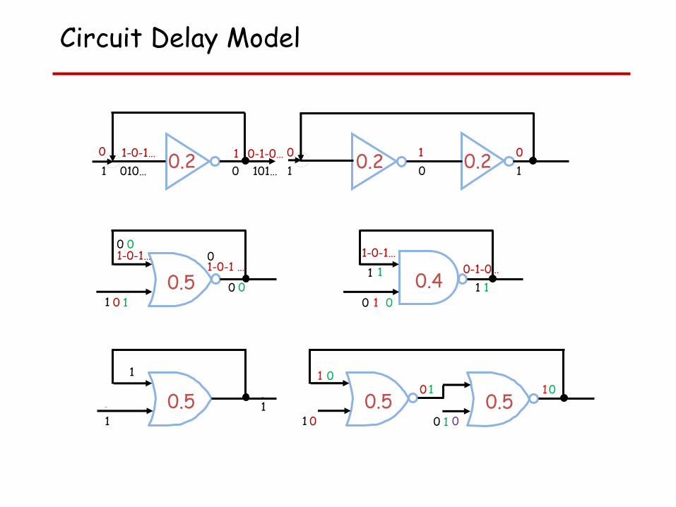
Circuit Delay Model
0
1
0.2 0.20.2
0 0.40
0-1-0…
1-0-1…
1
0.51
0
0
00.5
1
0.50
1
?1
0
1 010… 0 101…
0.50
00
1
00
1 1
1-0-1…1-0-1 … 1
1
0
0 11
1
0
0
1 0
1
1
1-0-1… 0-1-0…1 1 0
Storage Elements (Memory)
A storage element can maintain a binary state (0,1) indefinitely, until is directed by an input signal to switch state,
Main difference between storage elements:• Number of inputs they have
• How the inputs affect the binary state
Two main types:• Latches (level-sensitive)
• Flip-Flops (edge-sensitive)
Latches are useful in asynchronous sequential circuits
Flip-Flops are synchronous sequential circuits, built with latches
12
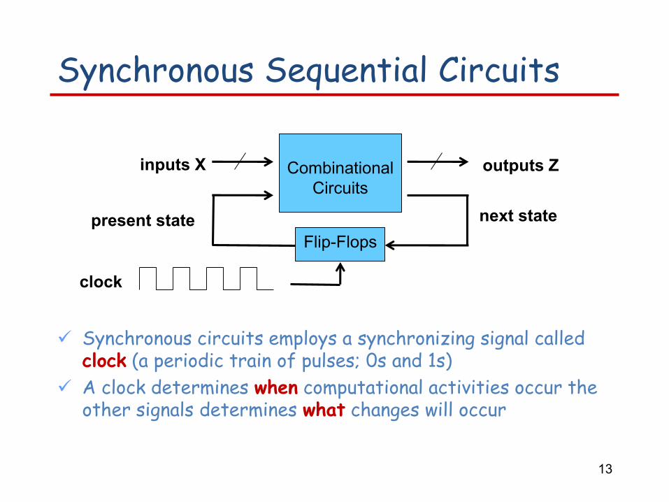
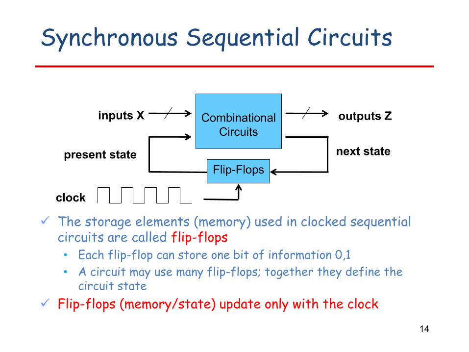
Synchronous Sequential Circuits
Synchronous circuits employs a synchronizing signal called clock (a periodic train of pulses; 0s and 1s)
A clock determines when computational activities occur the other signals determines what changes will occur
Combinational
Circuits
inputs X outputs Z
Flip-Flops
next statepresent state
clock
13
Synchronous Sequential Circuits
The storage elements (memory) used in clocked sequential circuits are called flip-flops• Each flip-flop can store one bit of information 0,1
• A circuit may use many flip-flops; together they define the circuit state
Flip-flops (memory/state) update only with the clock
14
Combinational
Circuits
inputs X outputs Z
Flip-Flops
next statepresent state
clock
Latches
15
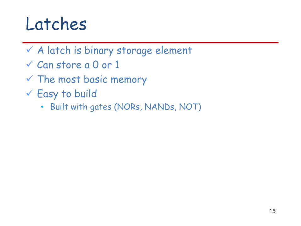
A latch is binary storage element
Can store a 0 or 1
The most basic memory
Easy to build • Built with gates (NORs, NANDs, NOT)
16
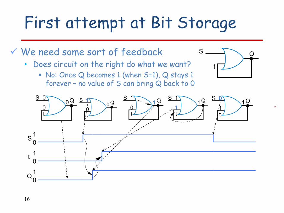
First attempt at Bit Storage
We need some sort of feedback• Does circuit on the right do what we want?
No: Once Q becomes 1 (when S=1), Q stays 1 forever – no value of S can bring Q back to 0
QS
t
0t
0Q
S0
1
0
1
0
1
0Q
t
S
0t
1Q
S0
0t
1Q
S1
1t
1Q
S1
1t
0Q
S1
a
17
0
0
1
R=1
S=0t
Q
1
0
1
0R
S
1
0t
1
0Q
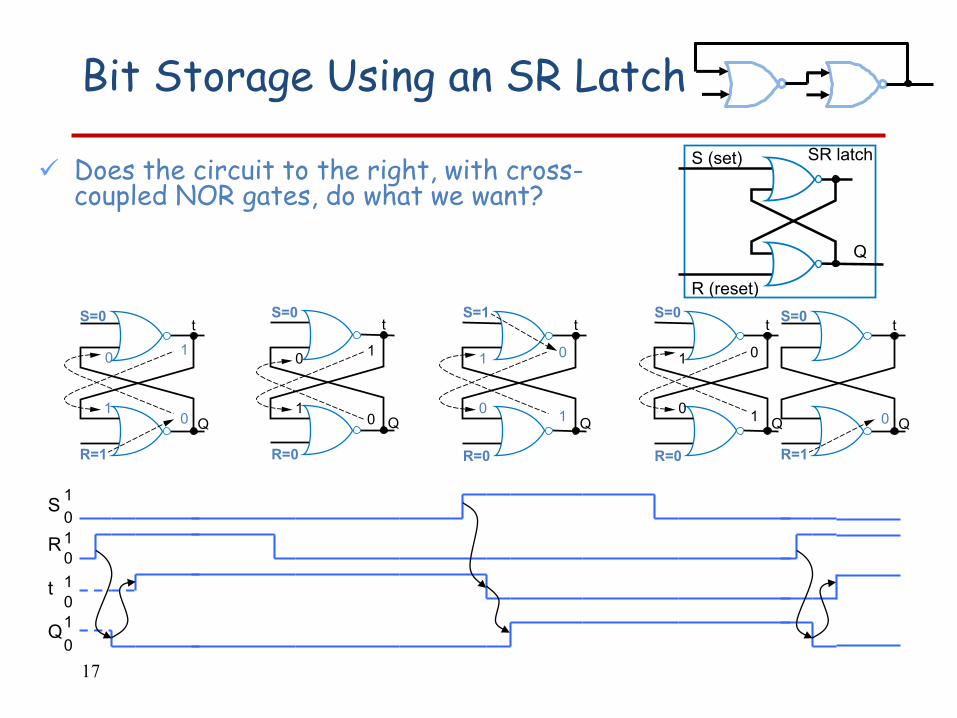
Bit Storage Using an SR Latch
Q
S (set) SR latch
R (reset)
Does the circuit to the right, with cross-coupled NOR gates, do what we want?
1
0 0
10
1
t
Q
S=0
R=0
t
Q
S=1
R=0
0
1
1
t
Q
R=0
S=0
1
01
0
R=1
S=0t
Q0
18
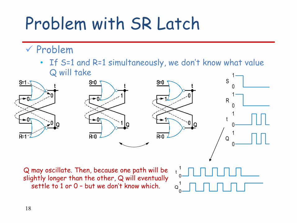
Problem with SR Latch
Problem• If S=1 and R=1 simultaneously, we don’t know what value
Q will take
0
1
0
1
0
1
0
1
S
R
Q
t
1t
0
1Q
0
Q may oscillate. Then, because one path will be slightly longer than the other, Q will eventually
settle to 1 or 0 – but we don’t know which.
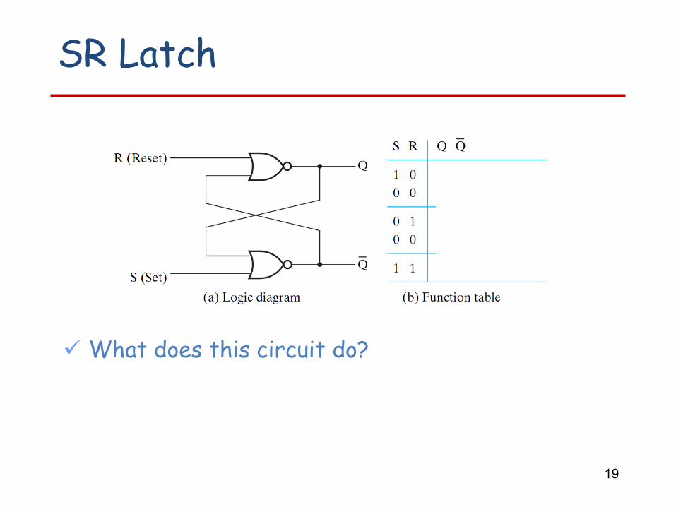
SR Latch
What does this circuit do?
19
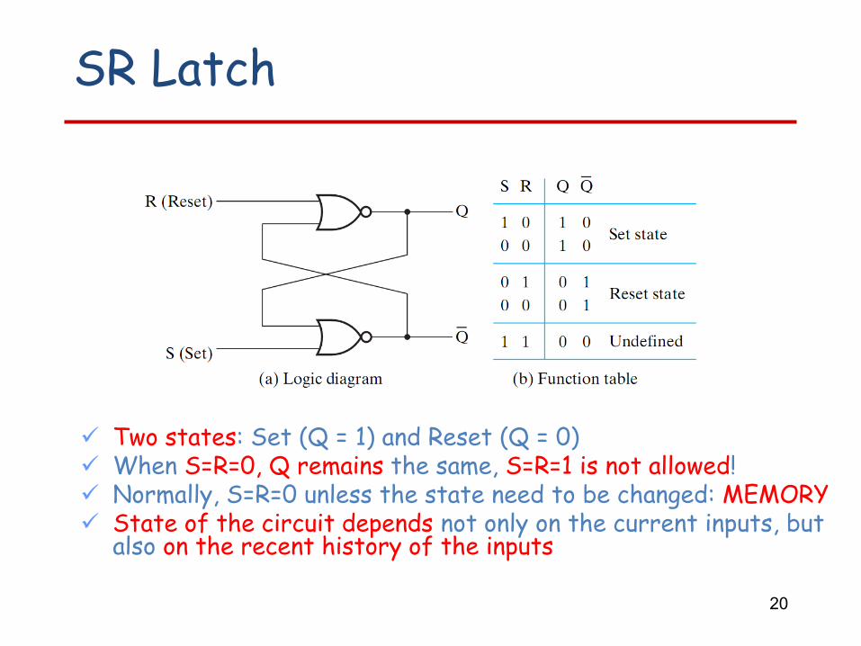
SR Latch
Two states: Set (Q = 1) and Reset (Q = 0) When S=R=0, Q remains the same, S=R=1 is not allowed! Normally, S=R=0 unless the state need to be changed: MEMORY State of the circuit depends not only on the current inputs, but
also on the recent history of the inputs
20
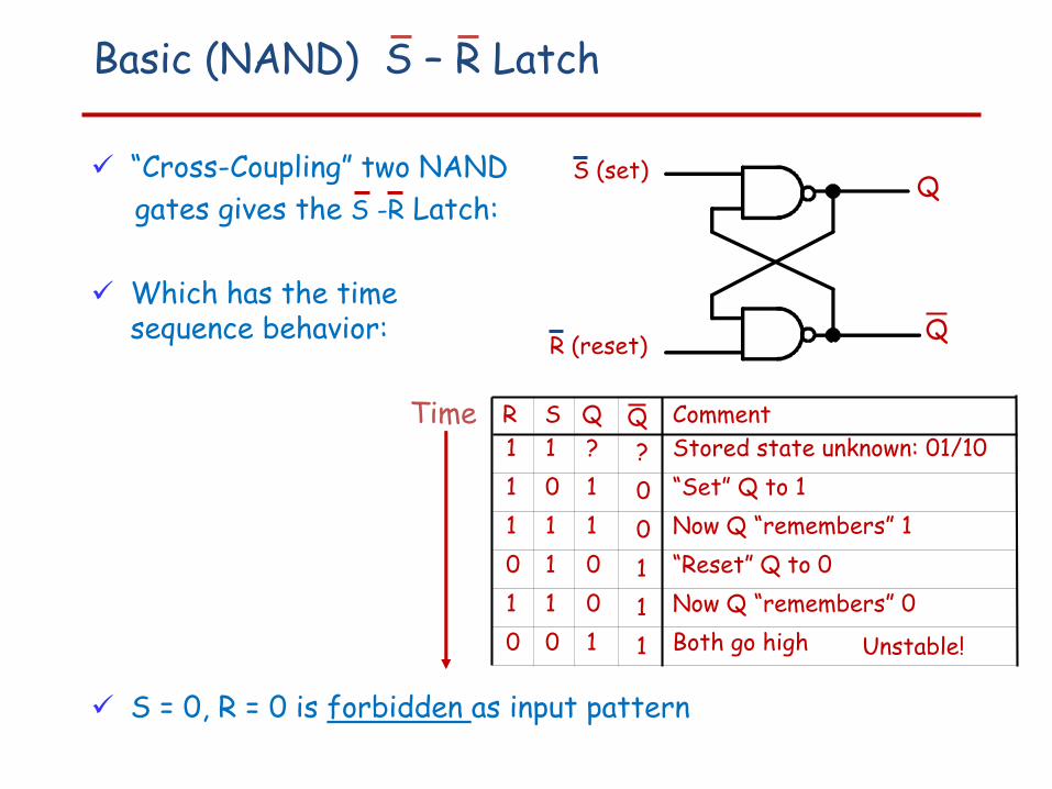
Basic (NAND) S – R Latch
“Cross-Coupling” two NAND
gates gives the S -R Latch:
Which has the time sequence behavior:
S = 0, R = 0 is forbidden as input pattern
S (set)
R (reset)
Q
Q
R S Q Q Comment
1 1 ? ? Stored state unknown: 01/10
1 0 1 0 “Set” Q to 1
1 1 1 0 Now Q “remembers” 1
0 1 0 1 “Reset” Q to 0
1 1 0 1 Now Q “remembers” 0
0 0 1 1 Both go high Unstable!
Time
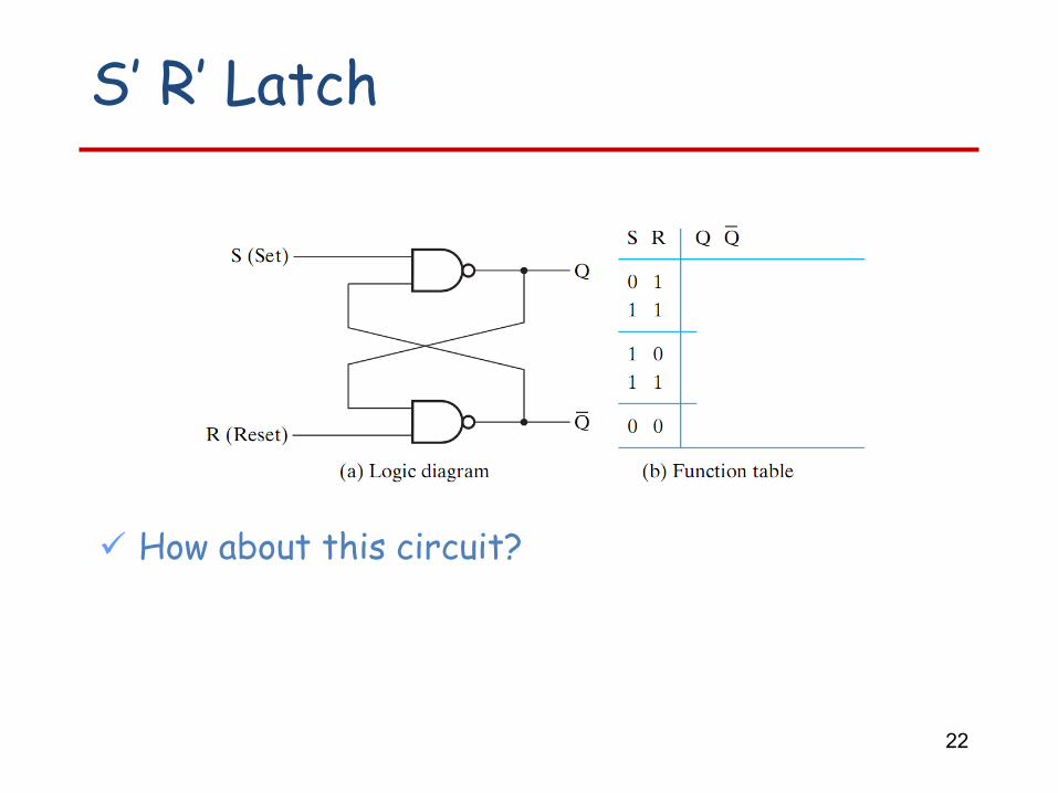
S’ R’ Latch
How about this circuit?
22
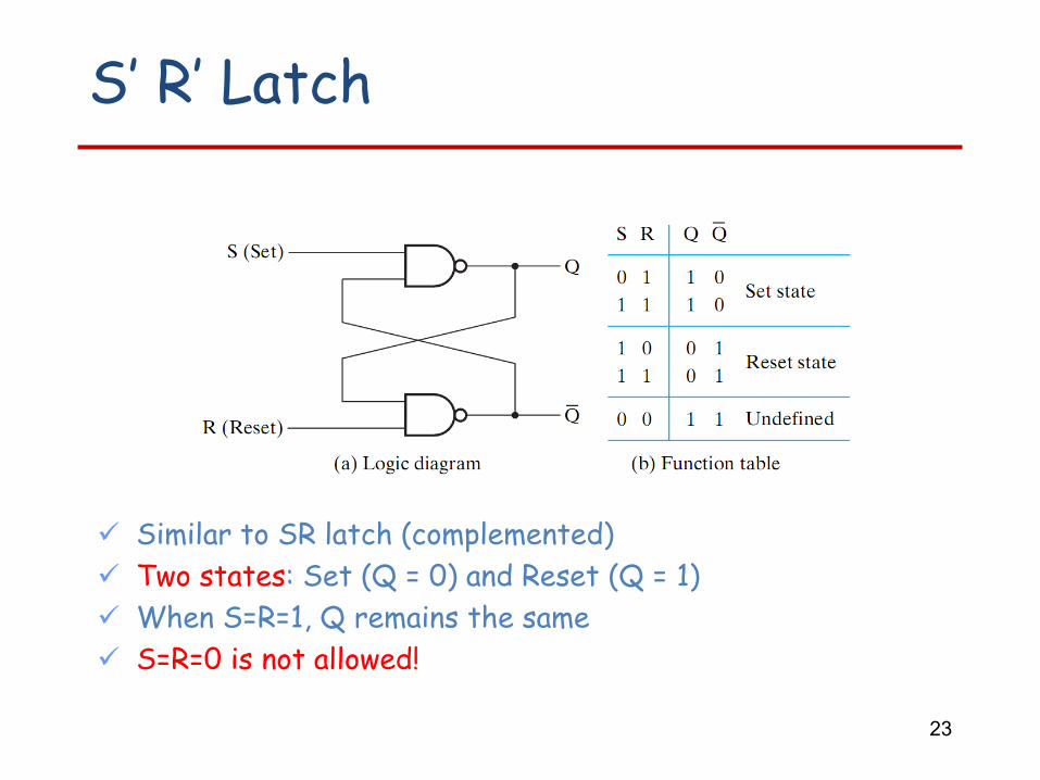
S’ R’ Latch
Similar to SR latch (complemented)
Two states: Set (Q = 0) and Reset (Q = 1)
When S=R=1, Q remains the same
S=R=0 is not allowed!
23
24
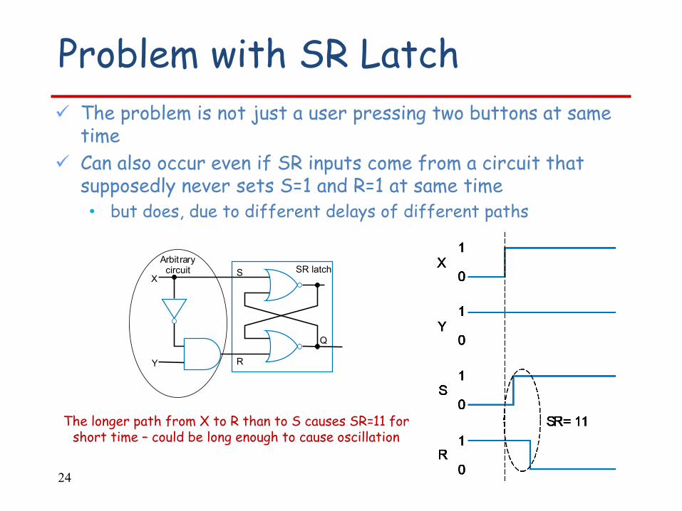
Problem with SR Latch
The problem is not just a user pressing two buttons at same time
Can also occur even if SR inputs come from a circuit that supposedly never sets S=1 and R=1 at same time• but does, due to different delays of different paths
The longer path from X to R than to S causes SR=11 for short time – could be long enough to cause oscillation
RY
XS SR latch
Q
Arbitrarycircuit
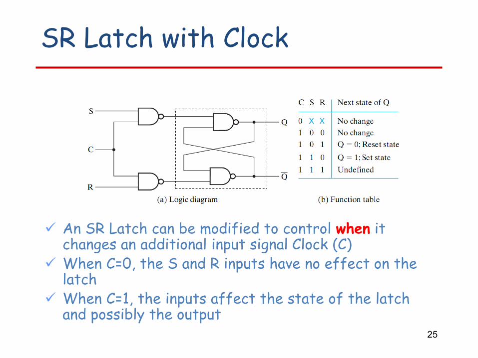
SR Latch with Clock
An SR Latch can be modified to control when it changes an additional input signal Clock (C)
When C=0, the S and R inputs have no effect on the latch
When C=1, the inputs affect the state of the latch and possibly the output
25
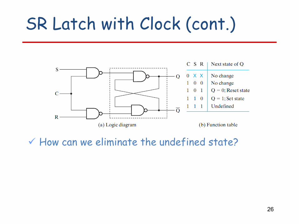
SR Latch with Clock (cont.)
How can we eliminate the undefined state?
26
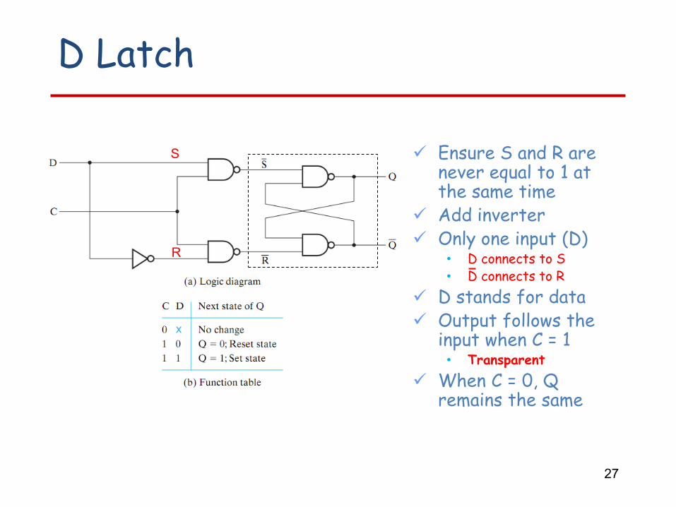
D Latch
Ensure S and R are never equal to 1 at the same time
Add inverter Only one input (D)
• D connects to S• D connects to R
D stands for data Output follows the
input when C = 1• Transparent
When C = 0, Q remains the same
R
S
27
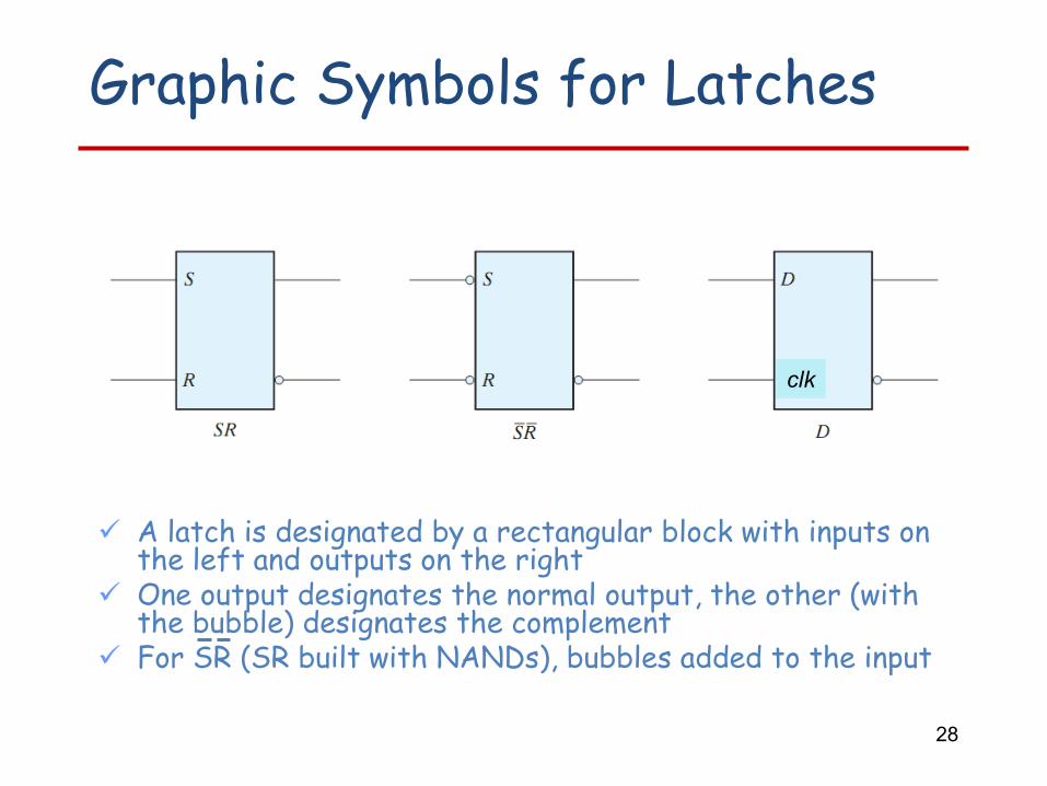
Graphic Symbols for Latches
A latch is designated by a rectangular block with inputs on the left and outputs on the right
One output designates the normal output, the other (with the bubble) designates the complement
For SR (SR built with NANDs), bubbles added to the input
clk
28
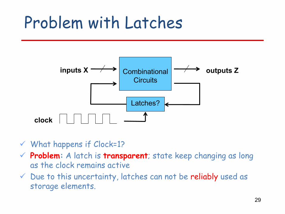
Problem with Latches
What happens if Clock=1?
Problem: A latch is transparent; state keep changing as long as the clock remains active
Due to this uncertainty, latches can not be reliably used as storage elements.
Combinational
Circuits
inputs X outputs Z
Latches?
clock
29
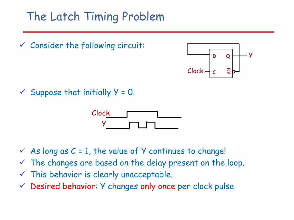
The Latch Timing Problem
Consider the following circuit:
Suppose that initially Y = 0.
As long as C = 1, the value of Y continues to change!
The changes are based on the delay present on the loop.
This behavior is clearly unacceptable.
Desired behavior: Y changes only once per clock pulse
Clock
Y
C
D Q
Q
Y
Clock
Flip Flops
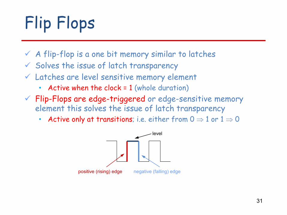
A flip-flop is a one bit memory similar to latches
Solves the issue of latch transparency
Latches are level sensitive memory element• Active when the clock = 1 (whole duration)
Flip-Flops are edge-triggered or edge-sensitive memory element this solves the issue of latch transparency• Active only at transitions; i.e. either from 0 1 or 1 0
31
positive (rising) edge negative (falling) edge
level
Flip Flops
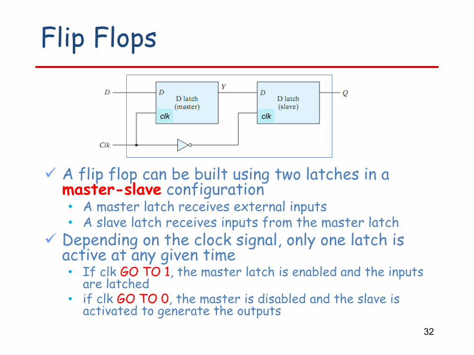
A flip flop can be built using two latches in a master-slave configuration• A master latch receives external inputs• A slave latch receives inputs from the master latch
Depending on the clock signal, only one latch is active at any given time• If clk GO TO 1, the master latch is enabled and the inputs
are latched• if clk GO TO 0, the master is disabled and the slave is
activated to generate the outputs
clkclk
32
Flip Flops
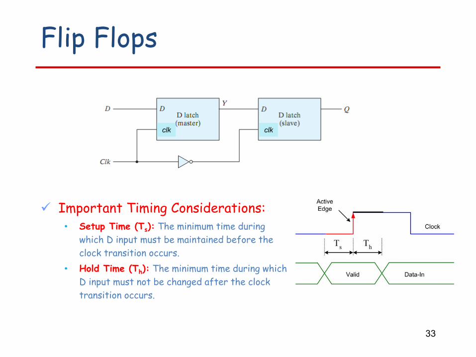
Important Timing Considerations:• Setup Time (Ts): The minimum time during
which D input must be maintained before the
clock transition occurs.
• Hold Time (Th): The minimum time during which
D input must not be changed after the clock
transition occurs.
clkclk
33
Edge-Triggered D Flip-Flop
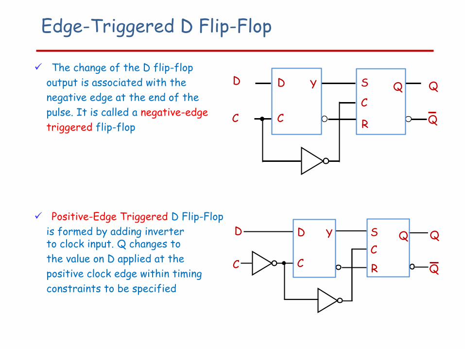
The change of the D flip-flop
output is associated with the
negative edge at the end of the
pulse. It is called a negative-edge
triggered flip-flop
Positive-Edge Triggered D Flip-Flop
is formed by adding inverterto clock input. Q changes to
the value on D applied at the
positive clock edge within timing
constraints to be specified
C
S
R
Q
C
Y
C
D QD
Q
C
S
R
Q
C
Y
C
D QD
Q
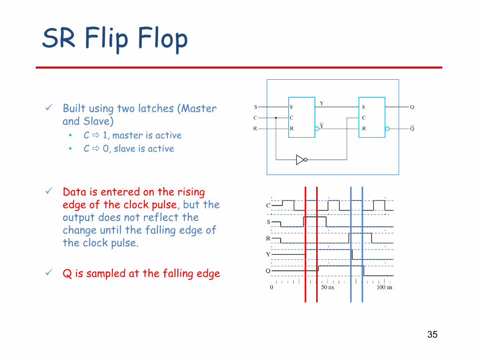
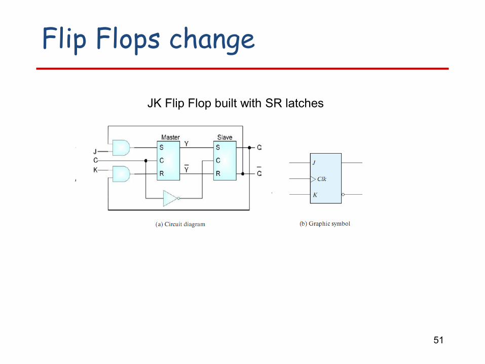
SR Flip Flop
Built using two latches (Master and Slave)• C 1, master is active
• C 0, slave is active
Data is entered on the rising edge of the clock pulse, but the output does not reflect the change until the falling edge of the clock pulse.
Q is sampled at the falling edge
35
36
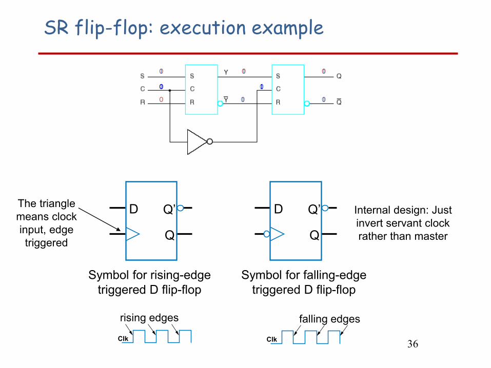
SR flip-flop: execution example
0
0
0
1
10
0
1
1
0
1
0
0
1
1
0
1
D Q’
Q
Q’D
Q
Symbol for rising-edge
triggered D flip-flop
Symbol for falling-edge
triggered D flip-flop
Clk
rising edges
Clk
falling edges
Internal design: Just
invert servant clock
rather than master
The triangle
means clock
input, edge
triggered
D-Type Positive-Edge-Triggered Flip-Flop
10
1
1
10
0
1
01
1
0
1 0
1
0
0
1
1
0
A
B
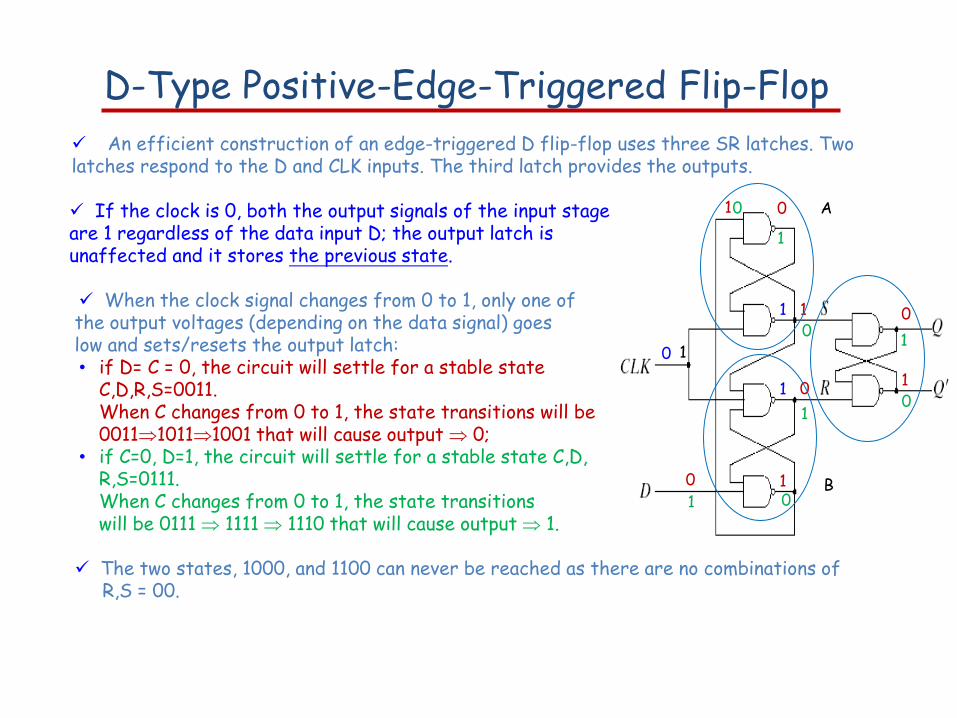
An efficient construction of an edge-triggered D flip-flop uses three SR latches. Two latches respond to the D and CLK inputs. The third latch provides the outputs.
If the clock is 0, both the output signals of the input stage are 1 regardless of the data input D; the output latch is unaffected and it stores the previous state.
When the clock signal changes from 0 to 1, only one ofthe output voltages (depending on the data signal) goes low and sets/resets the output latch:• if D= C = 0, the circuit will settle for a stable state
C,D,R,S=0011. When C changes from 0 to 1, the state transitions will be 001110111001 that will cause output 0;
• if C=0, D=1, the circuit will settle for a stable state C,D,R,S=0111. When C changes from 0 to 1, the state transitions will be 0111 1111 1110 that will cause output 1.
The two states, 1000, and 1100 can never be reached as there are no combinations ofR,S = 00.
Direct Inputs
Some flip-flops have asynchronous inputs that are used to force the flip-flop to a particular state independent of the clock.
The input that sets the flip-flop to 1 is called present or direct set.
The input that clears the flip-flop to 0 is called clear or direct reset.
When power is turned on a digital system, the state of the flip-flops is unknown. The direct inputs are useful for bringing all flip-flops in the system to a known starting state prior to the clocked operation.
39
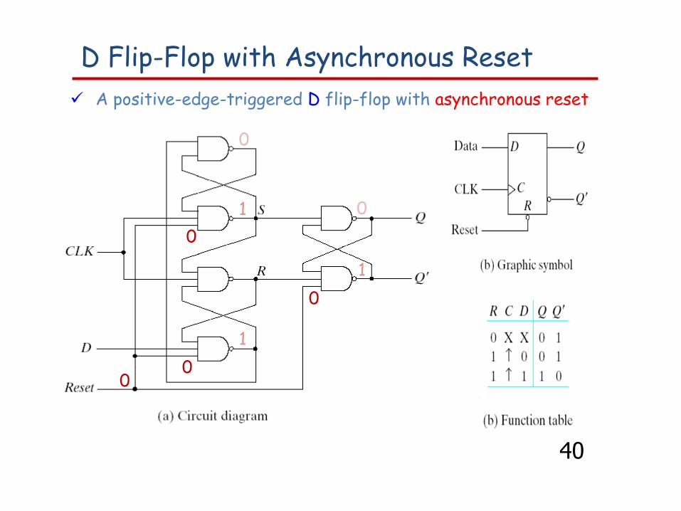
D Flip-Flop with Asynchronous Reset
40
A positive-edge-triggered D flip-flop with asynchronous reset
0
0
0
0
1
1
1
0
0
Other Flip-Flop Types
Description of J-K and T flip-flops:
• Behavior
• Implementation
Basic descriptors for understanding and using different flip-flop types:
• Characteristic table - defines the next state of the flip-flop in terms of flip-flop inputs and current state
• Characteristic equation - defines the next state of the flip-flop as a Boolean function of the flip-flop inputs and the current state
Used in design
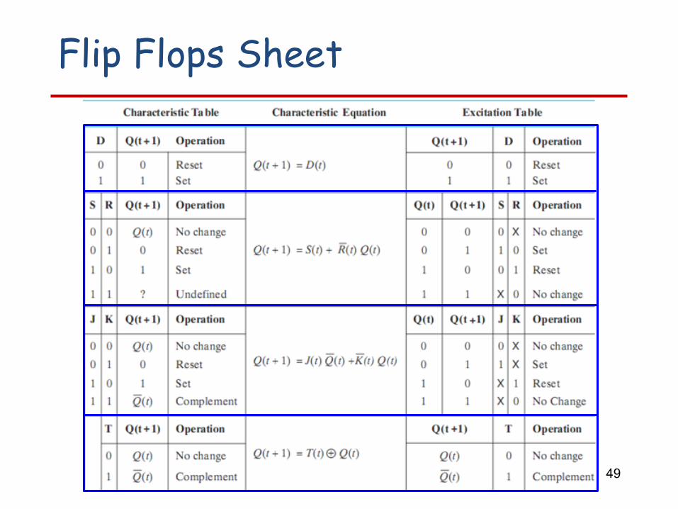
• Excitation table - defines the flip-flop input variable values as function of the current state and next state
J-K Flip-flop
Behavior:
• Same as S-R flip-flop with J analogous to S and K analogous to R
• Except that J = K = 1 is allowed, and For J = K = 1, the flip-flop changes to the
opposite state
T Flip-flop
Behavior:• Has a single input T
For T = 0, no change to state
For T = 1, changes to opposite state
Same as a J-K flip-flop with J = K = T
Cannot be initialized to a known state using the T input then: Reset is essential
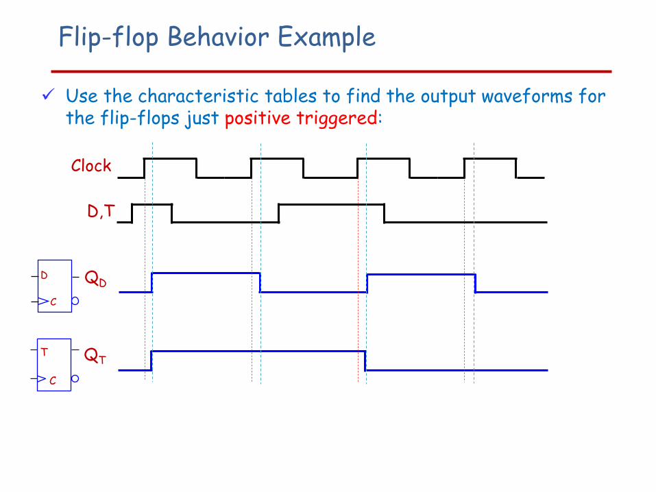
Flip-flop Behavior Example
Use the characteristic tables to find the output waveforms for the flip-flops just positive triggered:
T
C
Clock
D,T
QD
QT
D
C
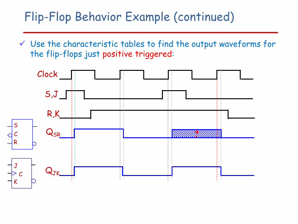
Flip-Flop Behavior Example (continued)
Use the characteristic tables to find the output waveforms for the flip-flops just positive triggered:
J
CK
S
C
R
Clock
S,J
QSR
QJK
R,K
?
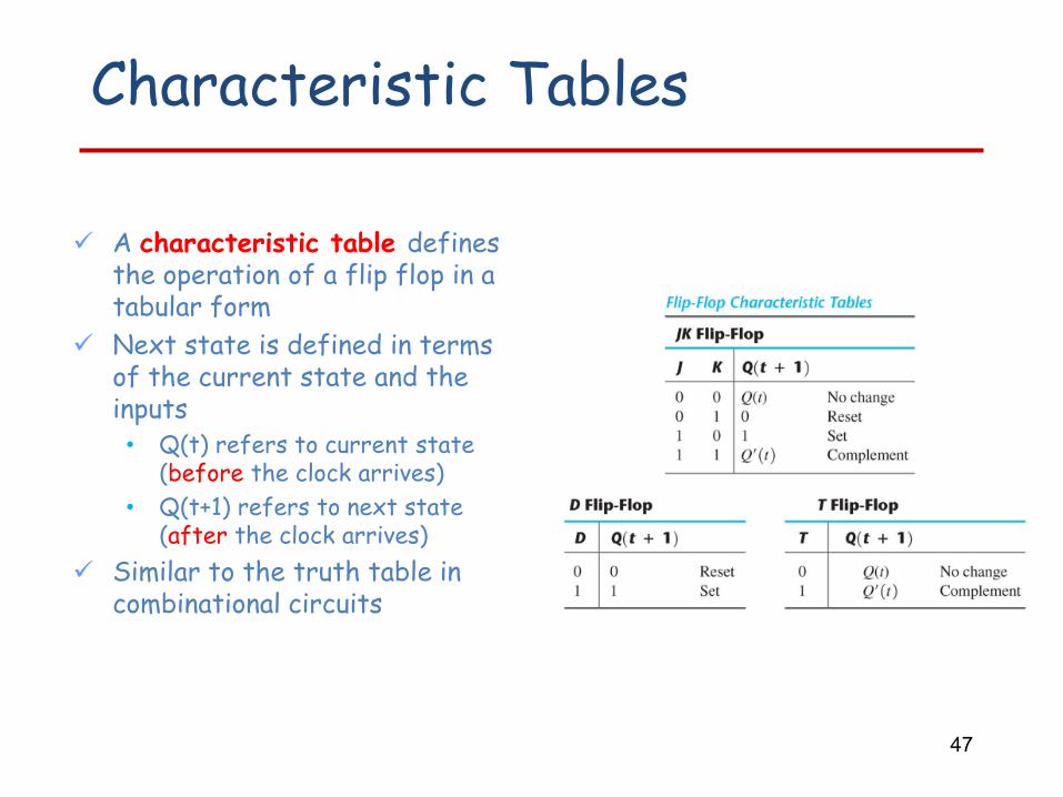
Characteristic Tables
A characteristic table defines the operation of a flip flop in a tabular form
Next state is defined in terms of the current state and the inputs• Q(t) refers to current state
(before the clock arrives)
• Q(t+1) refers to next state (after the clock arrives)
Similar to the truth table in combinational circuits
47
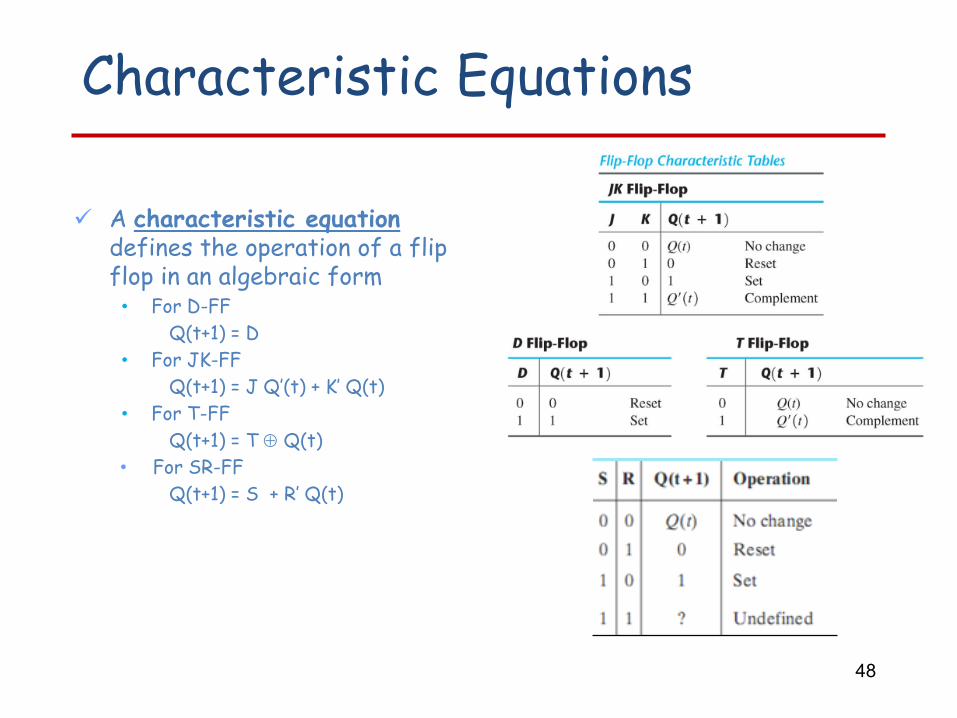
Characteristic Equations
A characteristic equation defines the operation of a flip flop in an algebraic form• For D-FF
Q(t+1) = D
• For JK-FF
Q(t+1) = J Q’(t) + K’ Q(t)
• For T-FF
Q(t+1) = T Q(t)
• For SR-FF
Q(t+1) = S + R’ Q(t)
48
Flip Flops Sheet
49
Flip Flops change
50
D to JK
JK to T D to T
Flip Flops change
JK Flip FlopJK Flip Flop built with SR latches
51
53
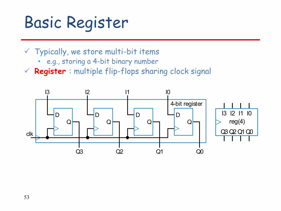
Basic Register
Typically, we store multi-bit items• e.g., storing a 4-bit binary number
Register : multiple flip-flops sharing clock signal
DQ
DQ
DQ
DQ
I2I3
Q2Q3 Q1 Q0
I1 I0
clk
4-bit register
I3 I2 I1 I0
Q3 Q2 Q1Q0
reg(4)
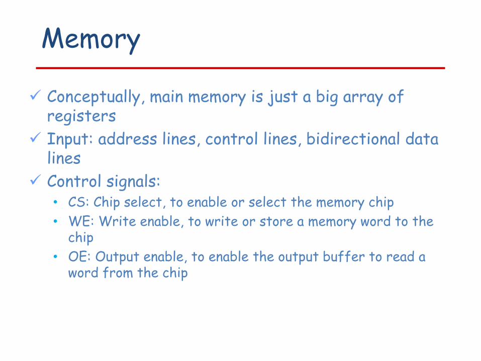
Memory
Conceptually, main memory is just a big array of registers
Input: address lines, control lines, bidirectional data lines
Control signals:• CS: Chip select, to enable or select the memory chip
• WE: Write enable, to write or store a memory word to the chip
• OE: Output enable, to enable the output buffer to read a word from the chip
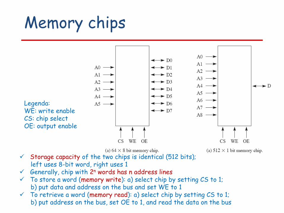
Memory chips
Storage capacity of the two chips is identical (512 bits);left uses 8-bit word, right uses 1
Generally, chip with 2n words has n address lines To store a word (memory write): a) select chip by setting CS to 1;
b) put data and address on the bus and set WE to 1 To retrieve a word (memory read): a) select chip by setting CS to 1;
b) put address on the bus, set OE to 1, and read the data on the bus
Legenda:WE: write enableCS: chip selectOE: output enable
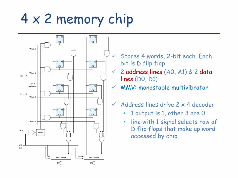
4 x 2 memory chip
Stores 4 words, 2-bit each. Each bit is D flip flop
2 address lines (A0, A1) & 2 data lines (D0, D1)
MMV: monostable multivibrator
Address lines drive 2 x 4 decoder
• 1 output is 1, other 3 are 0
• line with 1 signal selects row of D flip flops that make up word accessed by chip
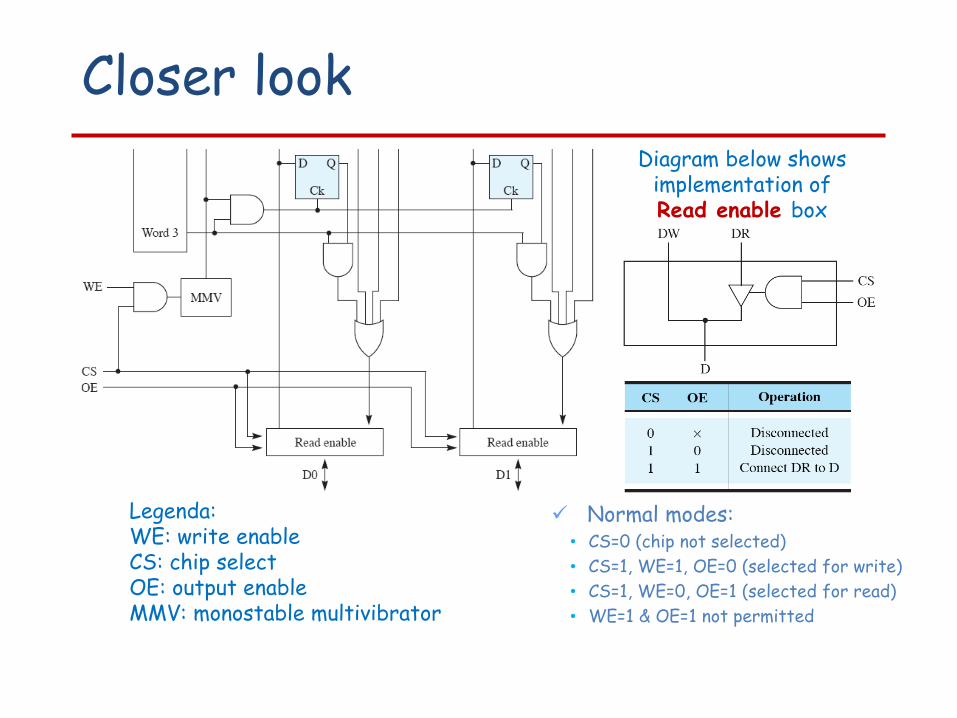
Closer look
Diagram below shows implementation of Read enable box
Legenda:WE: write enableCS: chip selectOE: output enableMMV: monostable multivibrator
Normal modes:• CS=0 (chip not selected)
• CS=1, WE=1, OE=0 (selected for write)
• CS=1, WE=0, OE=1 (selected for read)
• WE=1 & OE=1 not permitted
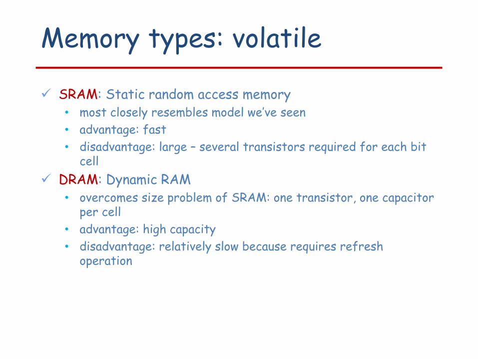
Memory types: volatile
SRAM: Static random access memory• most closely resembles model we’ve seen
• advantage: fast
• disadvantage: large – several transistors required for each bit cell
DRAM: Dynamic RAM• overcomes size problem of SRAM: one transistor, one capacitor
per cell
• advantage: high capacity
• disadvantage: relatively slow because requires refresh operation
Summary
In a sequential circuit, outputs depends on inputs and previous inputs• Previous inputs are stored as binary information into memory
• The stored information at any time defines a state
• Similarly, next state depends on inputs and present state
Two types of sequential circuits: Synchronous and Asynchronous
Two types of Memory elements: Latches and Flip-Flops.
Flip-flops are built with latches
A flip-flop is described using characteristic table/equation
60