Embed Size (px)
Citation preview
AS339/339A Document number: DS36838 Rev. 3 - 2
1 of 12 www.diodes.com
May 2018 © Diodes Incorporated
AS339/339A
LOW POWER LOW OFFSET VOLTAGE QUAD COMPARATORS
Description
The AS339/339A consist of four independent precision voltage
comparators with a typical offset voltage of 2.0mV and high gain.
They are specifically designed to operate from a single power supply
over wide range of voltages. Operation from split power supply is also
possible and the low power supply current drain is independent of the
magnitude of the power supply voltage.
The AS339/339A series are compatible with industry standard 339.
The AS339A has more stringent input offset voltage than the AS339.
The AS339 is available in SO-14 and TSSOP-14 packages, and the
AS339A is available in SO-14 package.
Features
Wide Supply Voltage Range
Single Supply: 2.0V to 36V
Dual Supplies: ±1.0V to ±18V
Low Supply Current Drain: 0.9mA
Low Input Bias Current: 25nA (Typical)
Low Input Offset Current: ±5.0nA (Typical)
Low Input Offset Voltage: 2.0mV (Typical)
Input Common Mode Voltage Range Includes Ground
Differential Input Voltage Range Equals to the Power Supply
Voltage
Low Output Saturation Voltage: 200mV at 4mA
Open Collector Output
Lead-Free Packages: SO-14, TSSOP-14
Totally Lead-Free; RoHS Compliant (Notes 1 & 2)
Lead-Free Packages, Available in “Green” Molding Compound:
SO-14, TSSOP-14
Totally Lead-Free & Fully RoHS Compliant (Notes 1 & 2)
Halogen and Antimony Free. “Green” Device (Note 3)
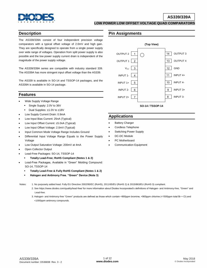
Pin Assignments
(Top View)
SO-14 / TSSOP-14
Applications
Battery Charger
Cordless Telephone
Switching Power Supply
DC-DC Module
PC Motherboard
Communication Equipment
Notes: 1. No purposely added lead. Fully EU Directive 2002/95/EC (RoHS), 2011/65/EU (RoHS 2) & 2015/863/EU (RoHS 3) compliant.
2. See https://www.diodes.com/quality/lead-free/ for more information about Diodes Incorporated’s definitions of Halogen- and Antimony-free, "Green" and
Lead-free.
3. Halogen- and Antimony-free "Green” products are defined as those which contain <900ppm bromine, <900ppm chlorine (<1500ppm total Br + Cl) and
<1000ppm antimony compounds.
INPUT 1-
1
2
3
4
5
6
7
14
13
12
11
10
9
8
INPUT 1+
INPUT 2-
INPUT 2+
OUTPUT 1
VCC
OUTPUT 3
OUTPUT 4
INPUT 4+
GND
INPUT 4-
INPUT 3+
INPUT 3-
OUTPUT 2
AS339/339A Document number: DS36838 Rev. 3 - 2
2 of 12 www.diodes.com
May 2018 © Diodes Incorporated
AS339/339A
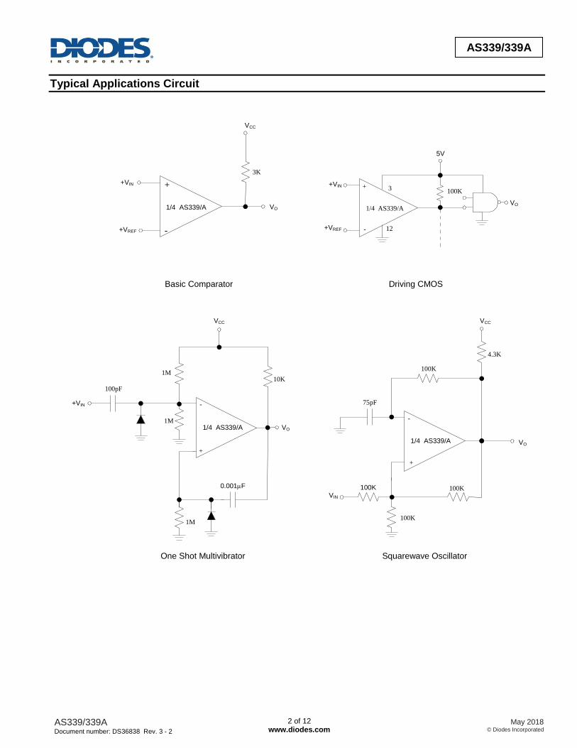
Typical Applications Circuit
Basic Comparator Driving CMOS
One Shot Multivibrator Squarewave Oscillator
+VIN
+VREF
1/4 AS339/A
VCC
3K
VO
+
-
100K
5V
+
- 12
3
1/4 AS339/A
+VIN
+VREF
VO
1M
1M
1M
VCC
VO
10K
-
+
+VIN
100pF
0.001F
1/4 AS339/A
100K
75pF
100K
VCC
4.3K
VO
100K
100K
-
+
VIN
1/4 AS339/A
AS339/339A Document number: DS36838 Rev. 3 - 2
3 of 12 www.diodes.com
May 2018 © Diodes Incorporated
AS339/339A
Functional Block Diagram
+INPUT
-INPUT
Q5 Q6
Q1
Q2 Q3
Q4
Q7
Q8OUTPUT
VCC
Absolute Maximum Ratings (Note 4)
Symbol Parameter Rating Unit
VCC Supply Voltage 40 V
VID Differential Input Voltage 40 V
VIN Input Voltage -0.3 to 40 V
IIN Input Current (VIN < -0.3V) (Note 5) 50 mA
— Output Short-Circuit to Ground Continuous —
PD Power Dissipation (TA = +25°C)
SO-14 890
mW
TSSOP-14 790
TJ Operating Junction Temperature +150 °C
TSTG Storage Temperature Range -65 to +150 °C
TLEAD Lead Temperature (Soldering, 10 Seconds) +260 °C
Notes: 4. Stresses greater than those listed under “Absolute Maximum Ratings” may cause permanent damage to the device. These are stress ratings only, and
functional operation of the device at these or any other conditions beyond those indicated under “Recommended Operating Conditions” is not implied.
Exposure to “Absolute Maximum Ratings” for extended periods may affect device reliability.
5. This input current will only exist when the voltage at any of the input leads is driven negative. It is due to the collector-base junction of the input PNP
transistors becoming forward biased and thereby acting as input diode clamps. In addition to this diode action, there is also lateral NPN parasitic
transistor action on the IC chip. This transistor action can cause the output voltages of the comparators to go to the V+ voltage level (or to ground for a
large overdrive) for the time duration that an input is driven negative. This is not destructive and normal output states will re-establish when the input
voltage, which was negative, again returns to a value greater than -0.3 VDC (at +25oC).
AS339/339A Document number: DS36838 Rev. 3 - 2
4 of 12 www.diodes.com
May 2018 © Diodes Incorporated
AS339/339A
Recommended Operating Conditions
Symbol Parameter Min Max Unit
VCC Supply Voltage 2 36 V
TA Operating Temperature Range -40 +85 °C
Electrical Characteristics (Limits in standard typeface are for TA = +25°C, bold typeface applies over TA = -40°C to +85°C (Note 6),
VCC = 5V, GND = 0V, unless otherwise specified.)
Notes: 6. Limits over the full temperature are guaranteed by design, but not tested in production.
7. The input common-mode voltage of either input signal voltage should not be allowed to go negatively by more than 0.3V (at +25°C). The upper end of the
common-mode voltage range is VCC -1.5V (at +25°C), but either or both inputs can go to +36V without damages, independent of the magnitude of the
VCC.
Parameter Conditions Min Typ Max Unit
Input Offset Voltage
VO = 1.4V, RS =
0Ω, VCC from 5V
to 30V
AS339 — 2 5
mV — — 7
AS339A — 2 3
— — 5
Input Bias Current IIN+ or IIN- with output in Linear Range,
VCM = 0V
— 25 250 nA
— — 400
Input Offset Current IIN+ - IIN-, VCM = 0V — 5.0 50
nA — — 200
Input Common Mode Voltage Range (Note
7) VCC = 30V 0 — VCC-1.5 V
Supply Current RL = ∞
VCC = 5V — 0.9 2.0
mA — — 3.0
VCC = 30V — 1.2 2.5
— — 3.5
Voltage Gain RL ≥ 15kΩ, VCC = 15V, VO = 1V to 11V 50 200 — V/mV
Large Signal Response Time VIN = TTL Logic Swing, VREF = 1.4V
VRL = 5V, RL = 5.1kΩ — 200 — ns
Response Time VRL = 5V, RL = 5.1kΩ — 1.3 — µs
Output Sink Current VIN- = 1V, VIN+ = 0, VO = 1.5V 6.0 16 — mA
Output Leakage Current VIN- = 0V, VIN+ = 1V, VO = 5V — 0.1 — nA
VIN- = 0V, VIN+ = 1V, VO = 30V — — 1 µA
Saturation Voltage VIN- = 1V, VIN+ = 0, ISINK ≤ 4mA — 200 400
mV — — 500
Thermal Resistance (Junction to Case) SO-14 — 15 —
°C/W TSSOP-14 — 6 —
Thermal Resistance (Junction to Ambient) SO-14 — 89 —
TSSOP-14 — 125 —
AS339/339A Document number: DS36838 Rev. 3 - 2
5 of 12 www.diodes.com
May 2018 © Diodes Incorporated
AS339/339A
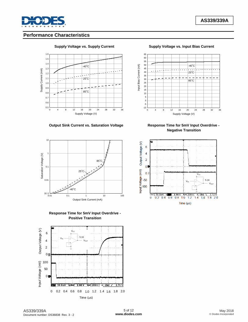
Performance Characteristics
Supply Voltage vs. Supply Current Supply Voltage vs. Input Bias Current
Output Sink Current vs. Saturation Voltage Response Time for 5mV Input Overdrive -
Negative Transition
Response Time for 5mV Input Overdrive -
Positive Transition
0 4 8 12 16 20 24 28 32 360.5
0.6
0.7
0.8
0.9
1.0
1.1
1.2
1.3
1.4
1.5
1.6
85oC
25oC
-40oC
Sup
ply
Cu
rre
nt (m
A)
Supply Voltage (V)
0 4 8 12 16 20 24 28 32 36-10
-5
0
5
10
15
20
25
30
35
40
45
50
55
60
65
85oC
25oC
-40oC
Inp
ut B
ias C
urr
en
t (n
A)
Supply Voltage (V)
0.01 0.1 1 10 1001E-3
0.01
0.1
1
10
85oC
25oC
-40oC
Satu
ratio
n V
olta
ge
(V
)
Output Sink Current (mA)
Time (s)
Inpu
t V
olta
ge
(m
V)
Outp
ut V
olta
ge
(V
)
0
6
4
2
50
0
100
1.8 2.01.4 1.61.0 1.20.6 0.80.2 0.40
VIN
VCC
5.1K
VOUT
+
_
VIN
VCC
5.1K
VOUT
+
_
AS339/339A Document number: DS36838 Rev. 3 - 2
6 of 12 www.diodes.com
May 2018 © Diodes Incorporated
AS339/339A
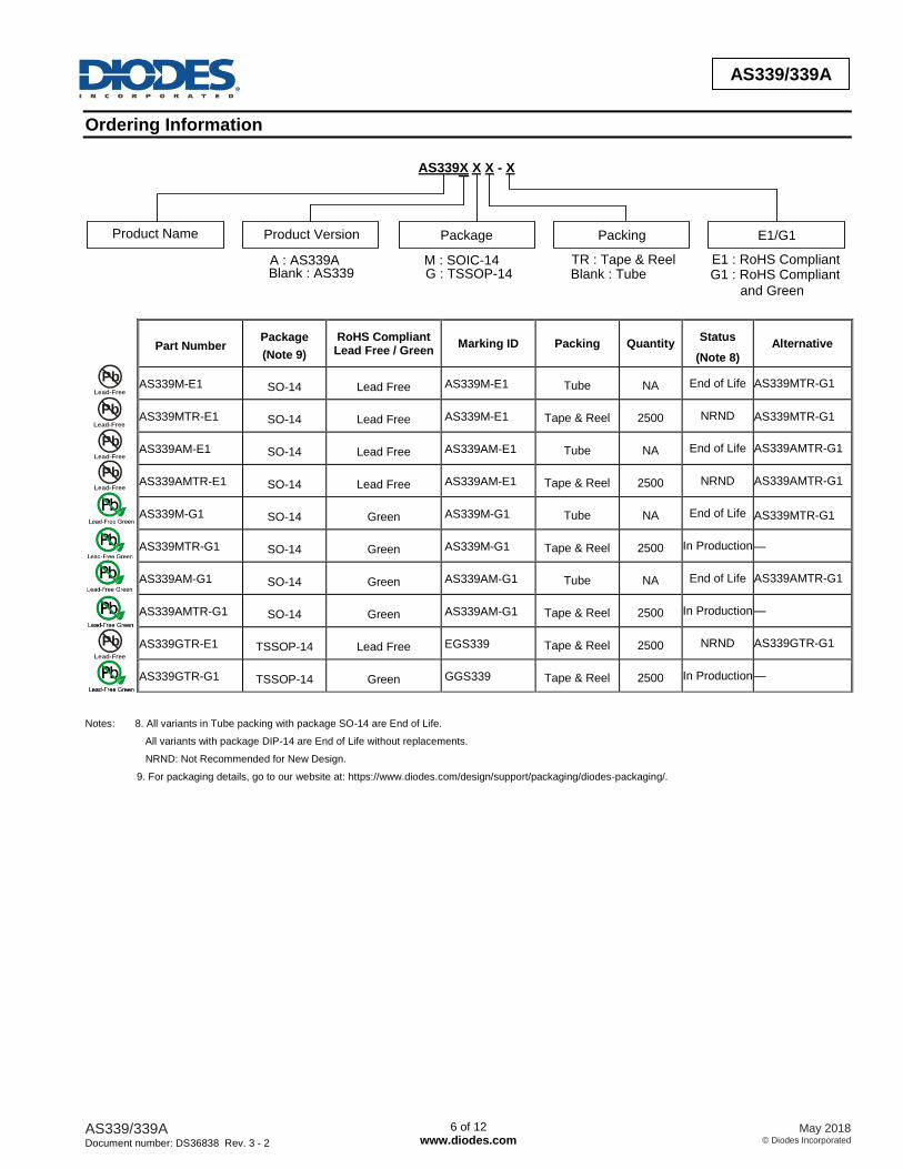
Ordering Information
AS339X X X - X
PackingPackage
TR : Tape & ReelA : AS339ABlank : AS339
Product Name
Blank : Tube
Product Version
G : TSSOP-14M : SOIC-14
E1/G1
E1 : RoHS CompliantG1 : RoHS Compliant
and Green
Notes: 8. All variants in Tube packing with package SO-14 are End of Life.
All variants with package DIP-14 are End of Life without replacements.
NRND: Not Recommended for New Design.
9. For packaging details, go to our website at: https://www.diodes.com/design/support/packaging/diodes-packaging/.
Part Number
Package
(Note 9)
RoHS Compliant Lead Free / Green
Marking ID Packing Quantity Status
(Note 8)
Alternative
AS339M-E1 SO-14 Lead Free AS339M-E1 Tube NA End of Life AS339MTR-G1
AS339MTR-E1 SO-14 Lead Free AS339M-E1 Tape & Reel 2500 NRND AS339MTR-G1
AS339AM-E1 SO-14 Lead Free AS339AM-E1 Tube NA End of Life AS339AMTR-G1
AS339AMTR-E1 SO-14 Lead Free AS339AM-E1 Tape & Reel 2500 NRND AS339AMTR-G1
AS339M-G1 SO-14 Green AS339M-G1 Tube NA End of Life AS339MTR-G1
AS339MTR-G1 SO-14 Green AS339M-G1 Tape & Reel 2500 In Production —
AS339AM-G1 SO-14 Green AS339AM-G1 Tube NA End of Life AS339AMTR-G1
AS339AMTR-G1 SO-14 Green AS339AM-G1 Tape & Reel 2500 In Production —
AS339GTR-E1 TSSOP-14 Lead Free EGS339 Tape & Reel 2500 NRND AS339GTR-G1
AS339GTR-G1 TSSOP-14 Green GGS339 Tape & Reel 2500 In Production —
PbLead-Free
PbLead-Free
PbLead-Free
PbLead-Free
PbLead-Free
AS339/339A Document number: DS36838 Rev. 3 - 2
7 of 12 www.diodes.com
May 2018 © Diodes Incorporated
AS339/339A
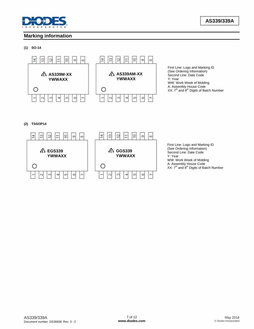
Marking information
(1) SO-14
(2) TSSOP14
First Line: Logo and Marking ID (See Ordering Information) Second Line: Date Code Y: Year WW: Work Week of Molding A: Assembly House Code XX: 7
th and 8
th Digits of Batch Number
AS339M-XX
YWWAXX
AS339AM-XX
YWWAXX
First Line: Logo and Marking ID (See Ordering Information) Second Line: Date Code Y: Year WW: Work Week of Molding A: Assembly House Code XX: 7
th and 8
th Digits of Batch Number
EGS339
YWWAXX
GGS339
YWWAXX
AS339/339A Document number: DS36838 Rev. 3 - 2
8 of 12 www.diodes.com
May 2018 © Diodes Incorporated
AS339/339A
Package Outline Dimensions (All dimensions in mm(inch).)
(1) Package Type: SO-14
Note: Eject hole, oriented hole and mold mark is optional.
8.550(0.337)
1.3
50(0
.053)
5°
7°
0.700(0.028)0.100(0.004)
0.250(0.010)
0.400(0.016)
0°
R0.200(0.008)
20:1
A
0.250(0.010)×45°
8°
A
8°
0.1
00(0
.00
4)
9.5°
8°
0°
8°
Depth 0.060(0.002)0.100(0.004)
2.000(0.079)
1.270(0.050)
1.0
00(0
.039)
1.3
00(0
.05
1)
5.8
00(0
.22
8)
8.750(0.344)
0.250(0.010)
1.7
50(0
.069)
0.2
50(0
.01
0)
3.800(0.150)
4.000(0.157)
0.310(0.012)
0.510(0.020)6.2
00(0
.24
4)
1.270(0.050)
8°
R0.200(0.008)
0.200(0.008)MIN
0.500(0.020)×45°
φ
15°
AS339/339A Document number: DS36838 Rev. 3 - 2
9 of 12 www.diodes.com
May 2018 © Diodes Incorporated
AS339/339A
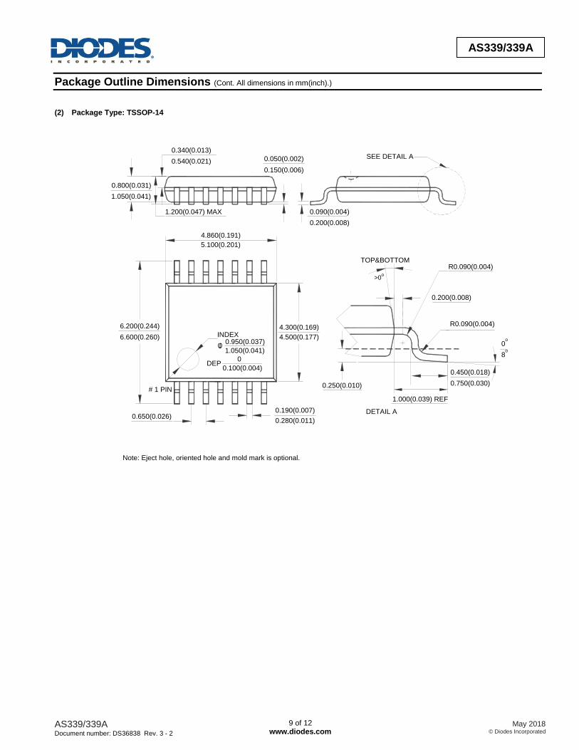
Package Outline Dimensions (Cont. All dimensions in mm(inch).)
(2) Package Type: TSSOP-14
Note: Eject hole, oriented hole and mold mark is optional.
SEE DETAIL A
DETAIL A
0
8
TOP&BOTTOM
1.000(0.039) REF
4.300(0.169)
4.500(0.177)
6.200(0.244)
6.600(0.260)
4.860(0.191)
5.100(0.201)
0.340(0.013)
0.540(0.021)
INDEX
0.050(0.002)
0.150(0.006)
0.800(0.031)
1.050(0.041)
0.650(0.026)0.190(0.007)
0.280(0.011)
0.250(0.010)
0.450(0.018)
0.750(0.030)# 1 PIN
0.950(0.037)
1.050(0.041)
DEP0
0.100(0.004)
0.090(0.004)
0.200(0.008)
R0.090(0.004)
R0.090(0.004)
0.200(0.008)
1.200(0.047) MAX
φ
>0o
o
o
AS339/339A Document number: DS36838 Rev. 3 - 2
10 of 12 www.diodes.com
May 2018 © Diodes Incorporated
AS339/339A
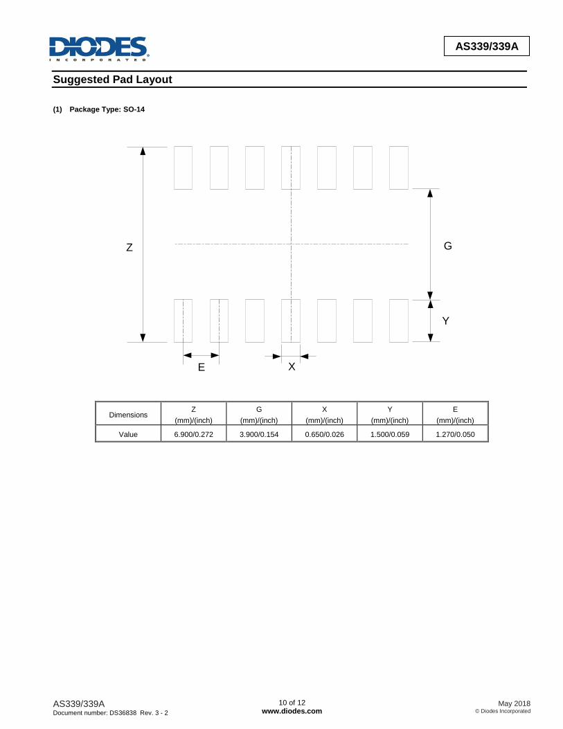
Suggested Pad Layout
(1) Package Type: SO-14
E X
Y
GZ
Dimensions Z
(mm)/(inch)
G
(mm)/(inch)
X
(mm)/(inch)
Y
(mm)/(inch)
E
(mm)/(inch)
Value 6.900/0.272 3.900/0.154 0.650/0.026 1.500/0.059 1.270/0.050
AS339/339A Document number: DS36838 Rev. 3 - 2
11 of 12 www.diodes.com
May 2018 © Diodes Incorporated
AS339/339A
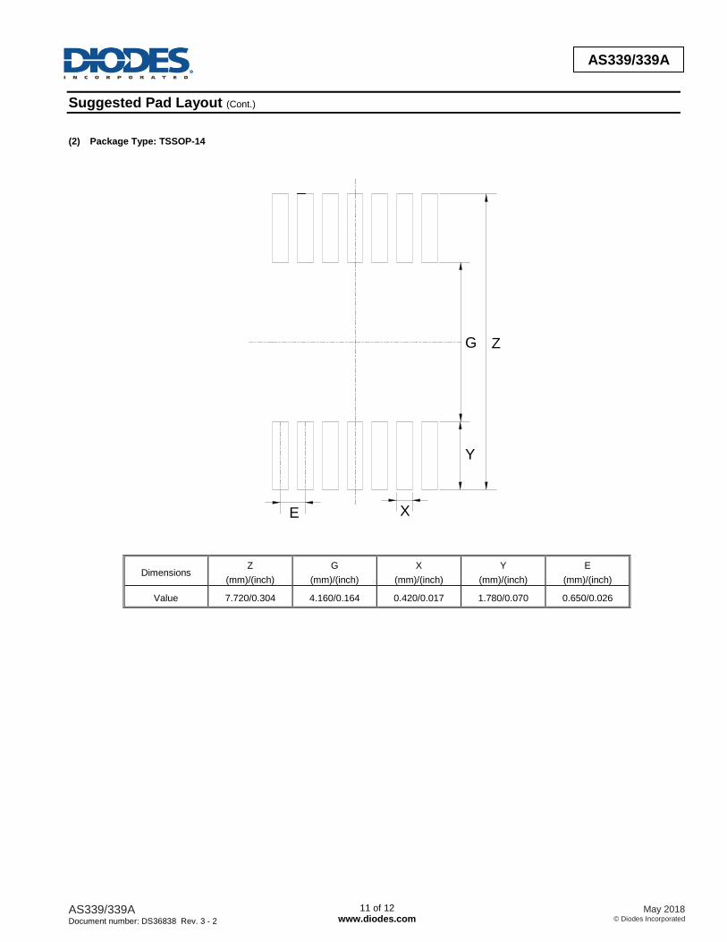
Suggested Pad Layout (Cont.)
(2) Package Type: TSSOP-14
E X
Y
G Z
Dimensions Z
(mm)/(inch)
G
(mm)/(inch)
X
(mm)/(inch)
Y
(mm)/(inch)
E
(mm)/(inch)
Value 7.720/0.304 4.160/0.164 0.420/0.017 1.780/0.070 0.650/0.026
AS339/339A Document number: DS36838 Rev. 3 - 2
12 of 12 www.diodes.com
May 2018 © Diodes Incorporated
AS339/339A
IMPORTANT NOTICE DIODES INCORPORATED MAKES NO WARRANTY OF ANY KIND, EXPRESS OR IMPLIED, WITH REGARDS TO THIS DOCUMENT, INCLUDING, BUT NOT LIMITED TO, THE IMPLIED WARRANTIES OF MERCHANTABILITY AND FITNESS FOR A PARTICULAR PURPOSE (AND THEIR EQUIVALENTS UNDER THE LAWS OF ANY JURISDICTION). Diodes Incorporated and its subsidiaries reserve the right to make modifications, enhancements, improvements, corrections or other changes without further notice to this document and any product described herein. Diodes Incorporated does not assume any liability arising out of the application or use of this document or any product described herein; neither does Diodes Incorporated convey any license under its patent or trademark rights, nor the rights of others. Any Customer or user of this document or products described herein in such applications shall assume all risks of such use and will agree to hold Diodes Incorporated and all the companies whose products are represented on Diodes Incorporated website, harmless against all damages. Diodes Incorporated does not warrant or accept any liability whatsoever in respect of any products purchased through unauthorized sales channel. Should Customers purchase or use Diodes Incorporated products for any unintended or unauthorized application, Customers shall indemnify and hold Diodes Incorporated and its representatives harmless against all claims, damages, expenses, and attorney fees arising out of, directly or indirectly, any claim of personal injury or death associated with such unintended or unauthorized application. Products described herein may be covered by one or more United States, international or foreign patents pending. Product names and markings noted herein may also be covered by one or more United States, international or foreign trademarks. This document is written in English but may be translated into multiple languages for reference. Only the English version of this document is the final and determinative format released by Diodes Incorporated.
LIFE SUPPORT Diodes Incorporated products are specifically not authorized for use as critical components in life support devices or systems without the express written approval of the Chief Executive Officer of Diodes Incorporated. As used herein: A. Life support devices or systems are devices or systems which: 1. are intended to implant into the body, or
2. support or sustain life and whose failure to perform when properly used in accordance with instructions for use provided in the labeling can be reasonably expected to result in significant injury to the user.
B. A critical component is any component in a life support device or system whose failure to perform can be reasonably expected to cause the failure of the life support device or to affect its safety or effectiveness. Customers represent that they have all necessary expertise in the safety and regulatory ramifications of their life support devices or systems, and acknowledge and agree that they are solely responsible for all legal, regulatory and safety-related requirements concerning their products and any use of Diodes Incorporated products in such safety-critical, life support devices or systems, notwithstanding any devices- or systems-related information or support that may be provided by Diodes Incorporated. Further, Customers must fully indemnify Diodes Incorporated and its representatives against any damages arising out of the use of Diodes Incorporated products in such safety-critical, life support devices or systems. Copyright © 2018, Diodes Incorporated www.diodes.com


![THE - Integra Energy Group · DC input power [W] Max. PV voltage [V] Rated input voltage [V] ... 160-280 480-800. 12. 13 Prepare ... activate the Emergency Power Supply (EPS)](https://img.pdfslide.us/doc/110x75/5af0cece7f8b9aa17b8f75b0/the-integra-energy-input-power-w-max-pv-voltage-v-rated-input-voltage-v.jpg)


![AC/DC SWITCHING POWER SUPPLY INPUT: 85~132VAC TRIPLE OUTPUT 8 WATTS ERS … · 2014. 8. 11. · Input Voltage Vac AC 100 V[DC 130 V] Input Voltage Range Vdc AC85~132V [DC110-175V]](https://img.pdfslide.us/doc/110x75/5fc9742a355705549e03215c/acdc-switching-power-supply-input-85132vac-triple-output-8-watts-ers-2014-8.jpg)